TOSHIBA FT-7800 Service Manual
Teléfonos
Precauciones de seguridad
Controles de operación
FT-7800
Procedimiento de ajuste
Diagramas a bloques
Diagramas esquemáticos
Consejos para localización de fallas
Tablas de voltajes en transistores e ICs
Identificación de terminales en semiconductores
Localización de partes eléctricas
Diagramas de alambrado
Vistas explotadas y lista de partes eléctricas
Lista de partes
Lista de partes para ensamblado
Especificaciones

FILE NO. 2B0-200001
SERVICE MANUAL
CORDLESS TELEPHONE
FT-7800
PUBLISHED IN JAPAN, June., 2000

CONTENTS
SAFETY PRECAUTIONS ............................................................................................................ 1
OPERATING CONTROLS........................................................................................................... 2
ALIGNMENT PROCEDURE ........................................................................................................ 3
BLOCK DIAGRAMS..................................................................................................................... 7
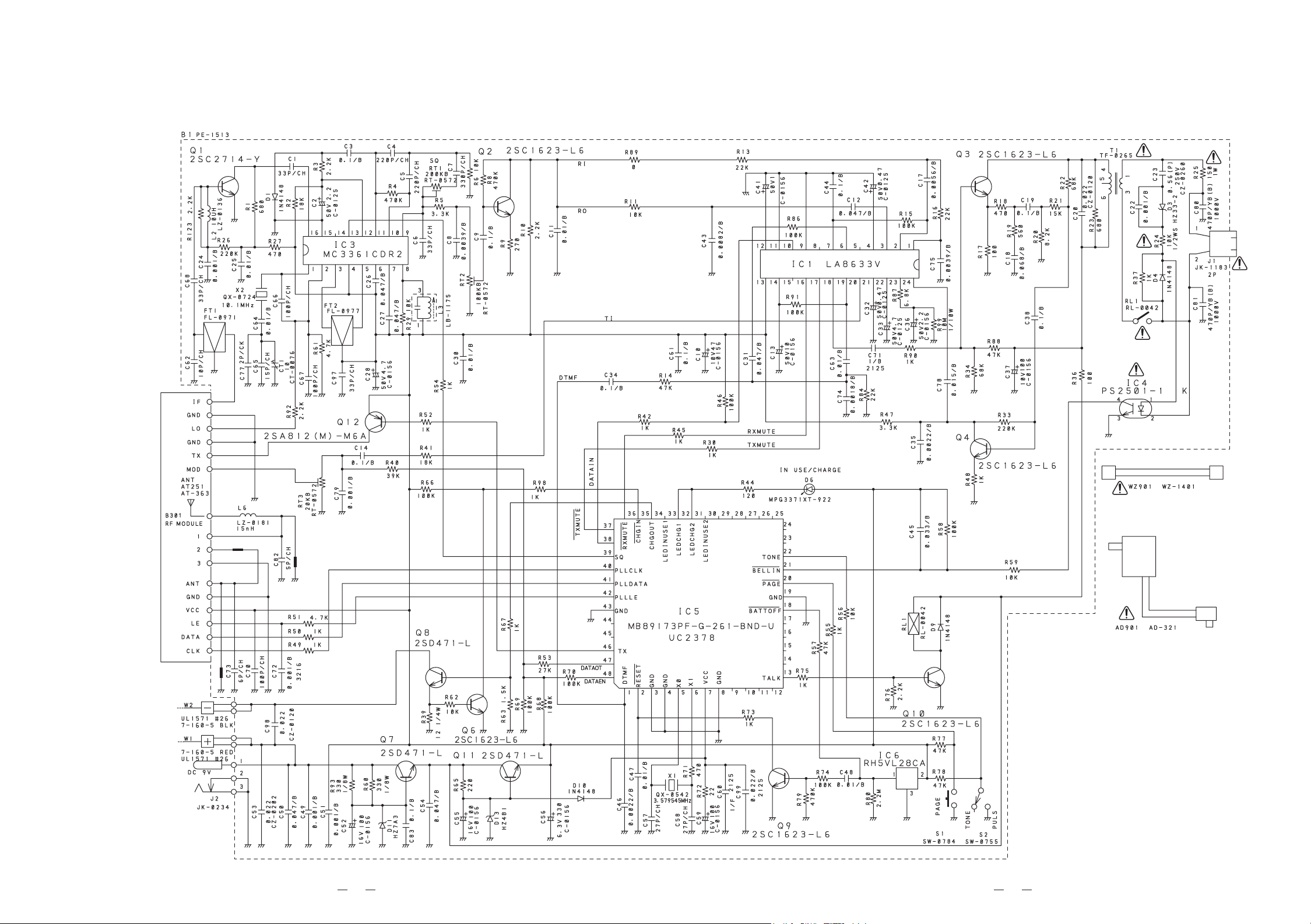
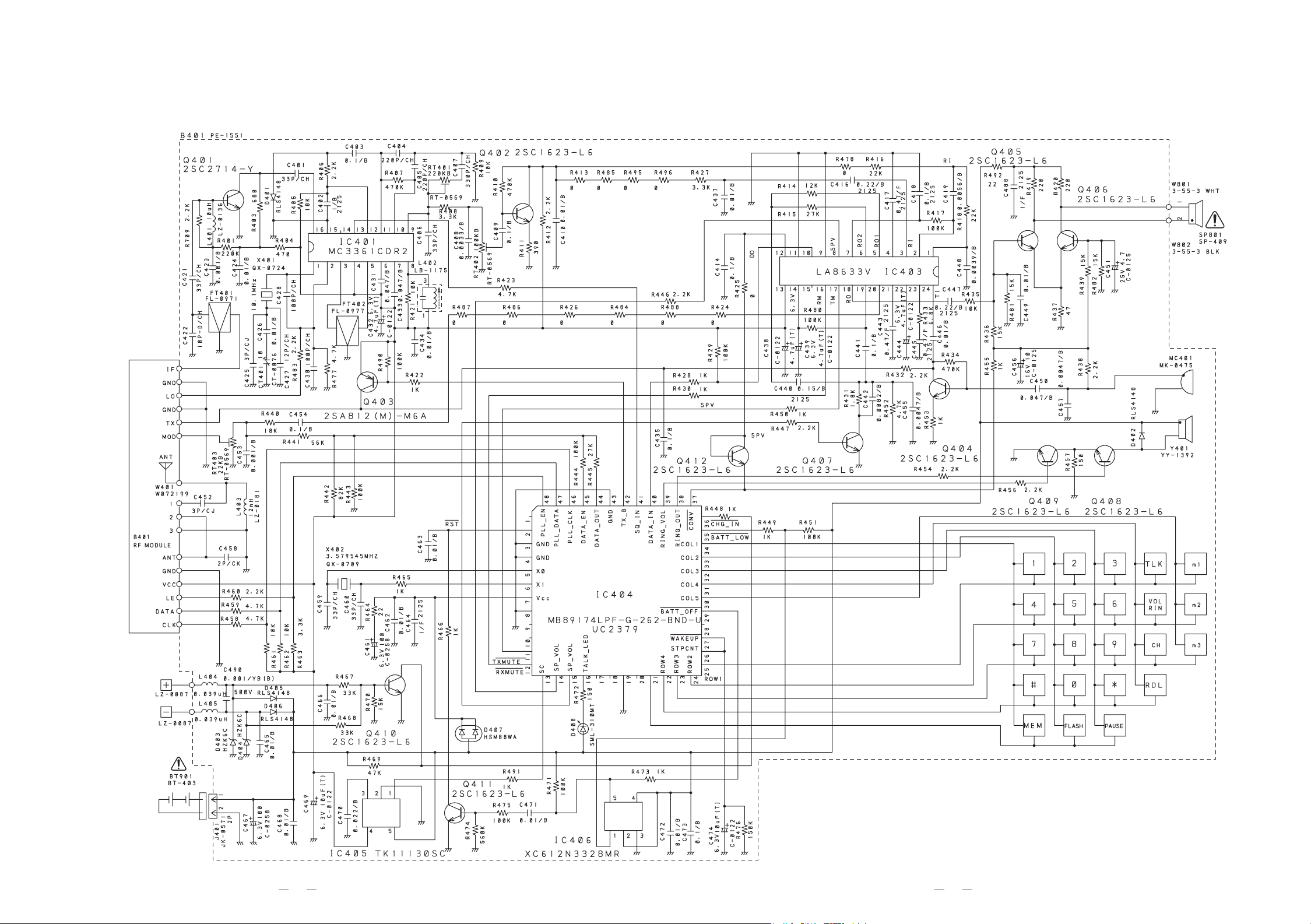
SCHEMATIC DIAGRAMS............................................................................................................9
TROUBLESHOOTING HINTS ...................................................................................................13
IC AND TRANSISTOR VOLTAGE CHART ............................................................................... 20
SEMICONDUCTOR LEAD IDENTIFICATION........................................................................... 24
ELECTRICAL PARTS LOCATION............................................................................................. 26
WIRING DIAGRAMS .................................................................................................................28
EXPLODED VIEW AND MECHANICAL PARTS LIST............................................................... 30
PARTS LIST............................................................................................................................... 34
ASSEMBLY PARTS LIST .......................................................................................................... 43
SPECIFICATIONS ..................................................................................................................... 44
SAFETY PRECAUTIONS
Before returning any models to the customer, a safety check of the entire instrument should be made.
The service technician must be sure that no protective device built into the instrument by the manufacture
has become defective or inadvertently degraded during servicing.
1.WARNING:
Alterations of the design or circuitry of these models should not be made.
Any design changes or additions such as, but not limited to, circuit modifications, auxiliary speaker
jacks, switches, grounding, active or passive circuitry, etc. may alter the safety characteristics of these
models and potentially create a hazardous situation for the user.
Any design alterations or additions will void the manufacturer's warranty and will further relieve the
manufacturer of responsibility for personal injury or property damage resulting therefrom.
2.PRODUCT SAFETY NOTICE
Many electrical and mechanical parts in this chassis have special characteristics. These characteristics
often pass unnoticed and the protection afforded by them cannot necessarily be obtained by using
replacement components rated for higher voltage, wattage, etc. Replacement parts that have these
special safety characteristics are identified in this manual and its supplements; electrical components
having such features are indentified by a
any of these components, read the parts list in this manual carefully. The use of substitute replacement
parts that do not have the same safety characteristics as specified in the parts list may create shock, fire
or other hazards.
in the schematic diagram and the parts list. Before replacing
1
OPERATING CONTROLS
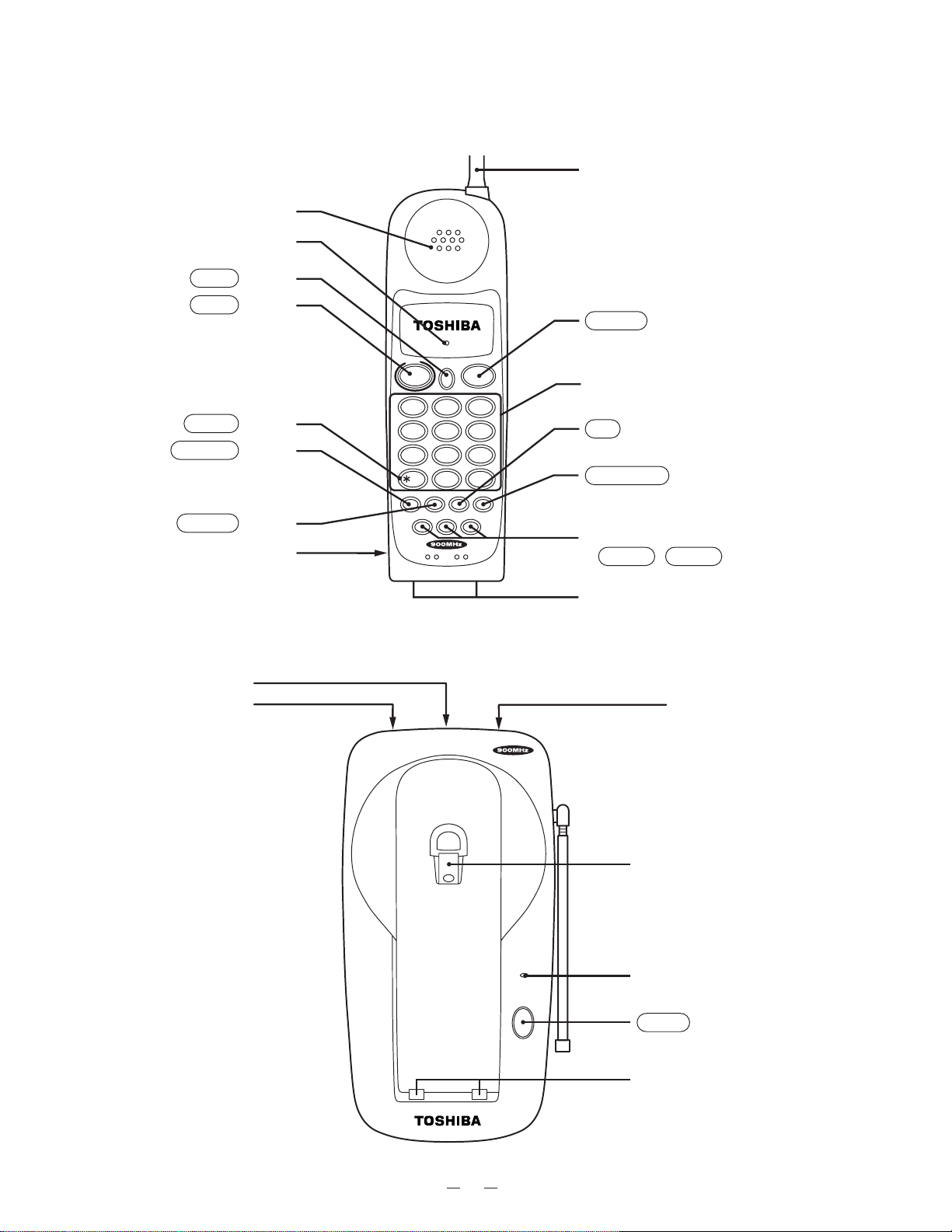
HANDSET CONTROLS AND FUNCTIONS
Speaker
TALK/BATT.LOW LED
MEM button
TALK button
TALK
BATT LOW
TALK FLASH
MEM
abc def
123
TONE button
REDIAL button
PAUSE button
Rechargeable Battery Pack
(back)
456
789
TONE
REDIAL
PAUSE CH VOL/RING
MEM1 MEM2 MEM3
mno
jklgfi
tuvpqrs
wxyz
oper
0
#
Antenna
FLASH button
Dialpad
CH button
VOL/RING button
One-touch dialing button
( MEM1 - MEM3 )
BASE UNIT CONTROLS AND FUNCTIONS
DC In 9V Jack
TEL LINE Jack
IN USE
CHARGE
PAGE
Charging Contacts
T-P (TONE-PULSE) Switch
Hook
IN USE/CHARGE LED
PAGE button
Charging Contacts
2
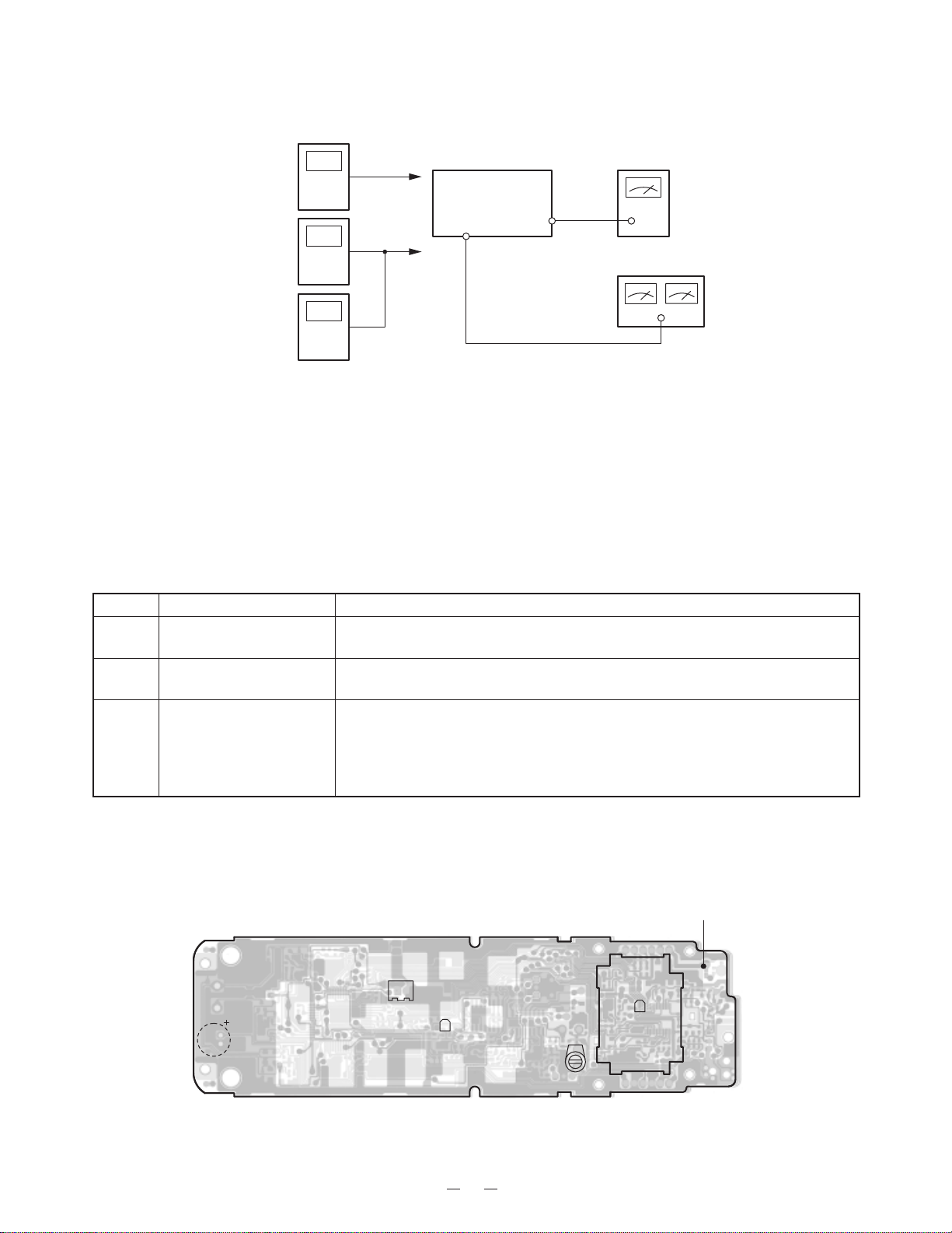
ALIGNMENT PROCEDURE
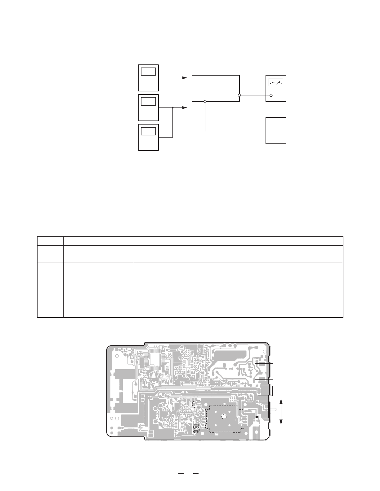
Base Unit
Transmitter Section
Connections
Power
Meter
Frequency
Counter
Deviation
Mater
RF
Test Point
RF
Test Point
Preset
a) Connect the base RF unit to the base main unit.
b) Set the “T ONE / PULSE” switch to PULSE.
c) Connect the AC adapter to the base unit while pressing the “PAGE” key, and keep pressing it continuously for
approximate 2 sectonds.
d) Release the “PAGE” key when entering TEST mode 1 with IN USE LED lighting.
BASE Unit
J2
DC IN
9V Jack
TEL Line
Jack
J1
1kHz 77.5mV
AF GEN.
AC
Adapter
AC 120V
60Hz
Alignment Procedure
step
1
2
3
Adjustment
RT301
(TX Po wer)
CT1
(TX Frequency)
RT3
(TX Modulation)
Remarks
Connect the Po w er Meter to the RF test point on the Base MAIN PCB.
Adjust RT301 for a -7.5dBm reading on the Power Meter.
Connect the Frequency Counter to the RF test point on the Base MAIN
PCB. Adjust CT1 to make sure that the frequency is 926.897468 MHz.
Press the “PA GE” k ey to enter the TEST Mode 2. Connect the AF Generator
to the TEL Line J a ck on the Base Main PCB. Make sure that the output is 1
kHz 77.5 mV from the AF Generator .
Connect the Deviation Meter to the RF test point on the Base MAIN PCB .
Adjust RT3 to indicate ±8 kHz Dev.
Alignment Point Location on Base Main PCB and Base RF PCB
Base Main PCB
RT3
Base RF PCB
RT301
CT1
J1
TEL LINE Jack
J2
DC IN 9V Jack
T
S2
T/P Switch
P
RF Test Point
3
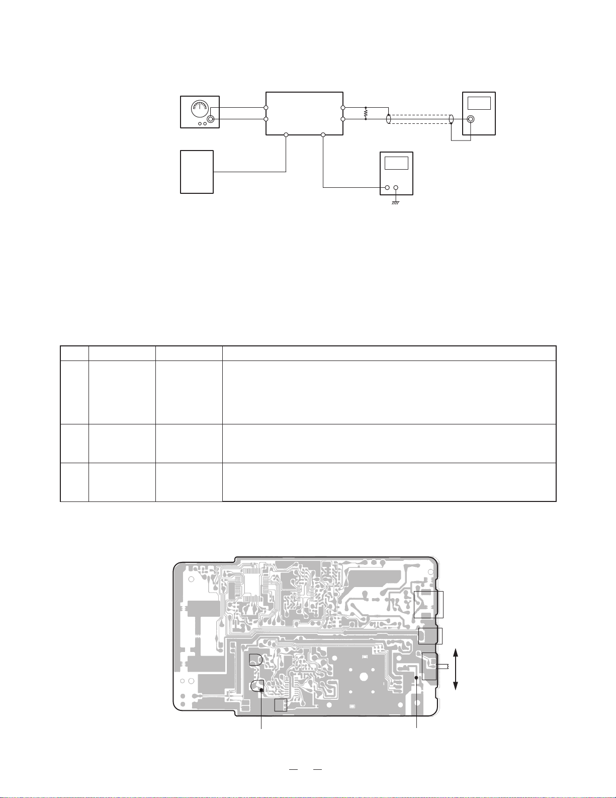
Receiver Section
Connections
RF SG
+
RF
Test Point
TEL Line
Jack
J1
Dummy Load
(600-ohm)
+
AC V oltmeterBASE Unit
AC 120V
60Hz
AC
Adapter
DC IN 9V Jack
J2
AF
Terminal
DC V oltmeter
Preset
a) Connect the base RF unit to the base main unit.
b) Set the “TONE/PULSE” switch to PULSE.
c) Connect the AC adapter to the base unit while pressing the “PAGE” key, and keep pressing it continuously for
approximate 2 seconds.
d) Release the “PAGE” key when entering TEST mode 1 with IN USE LED lighting.
Alignment Procedure
step
Preset to
1
SG: 1mV
No modulation
SG: 1mV
1 kHz ±8kHz
2
deviation
SG: -6.0 dB
1kHz ±8kHz
3
Deviation
Adjustment
(Discriminator
Voltage)
(RX AF
Voltage)
µµ
µV
µµ
(SQ Point)
L3
RT2
RT1
Remarks
Press the “PAGE” key for 3 times to enter the TEST Mode 4. Connect the
RF Signal Generator to the RF test point on the Base MAIN PCB. Make
sure that the frequency is 902.952467 MHz.
Connect the DC Voltmeter to the AF test point. Adjust L3 to indicate DC
1.00 V.
Connect the AC Voltmeter across a 600-ohm dummy to the Telephone Line
Jack. Adjust RT2 for a 220 mV reading on the AC voltmeter.
Press the “PAGE” key to enter the TEST Mode 5. Make sure that the
frequency of RF SG output is 902.952467 MHz. Adjust RT1 to turn to the
point where the CHG LED just turns on.
Alignment Point Location on Base Main PCB and Base RF PCB
Base Main PCB
RT2
RT1
L3
AF Test Point
4
J1
TEL LINE Jack
J2
DC IN 9V Jack
T
S2
T/P Switch
P
RF Test Point
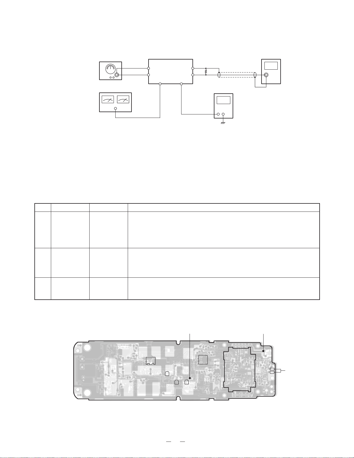
Handset Unit
Transmitter Section
Connection
Power
Meter
Frequency
Counter
Deviation
Mater
RF
Test Point
RF
Test Point
HANDSET Unit
J401
Battery
Connector
MIC+Pin
AF GEN.
1kHz 9mV
DC Power Supply
DC 3.8V
Preset
a) Connect the handseet RF unit to the handset main unit.
b) Connect DC power supply to battery connector on the handset unit.
c) Turn the DC power supply On while pressing " ∗ " and " # " keys, and keep pressing the keys continuously for
approximate 2 seconds.
d) Release keys when entering TEST mode 1 with TALK LED lighting and beep.
Alignment Procedure
step
1
2
Adjustment
RT501
(TX Po wer)
CT401
(TX Frequency)
Remarks
Connect the RF power Meter to the RF test point on the handset MAIN PCB.
Adjust RT501 for a -7.5dBm reading on the Power Meter.
Connect the Frequency Counter to the RF test point on the handset MAIN
PCB. Adjust CT401 to make sure that the frequency is 903.052467 MHz.
Press the “2” key to enter the TEST Mode 2. Connect the AF Generator to
3
RT403
(TX Modulation)
the MIC Connector. Make sure that the output is 1kHz 8mV from the AF
Generator.
Connect the Deviation Meter to the RF test point on the handset MAIN PCB.
Adjust RT403 to indicate ±8 kHz De v.
Alignment Point Location on Handset Main PCB and Handset RF PCB
Handset PCB
MC601
J401
RT403
CT401
RF PCB
RT501
RF Test Point
5
Receiver Section
Connections
RF SG
RF
Test PointSPTerminal
+
Dummy Load
(150-ohm)
WHT
BLK
AC V oltmeterHANDSET Unit
DC Power Supply
J401
Battery
Connector
DC 3.8V
AF
Test Point
DC V oltmeter
Preset
a) Connect the handset RF unit to the handset main unit.
b) Connect DC power supply to battery connector on the handset unit.
c) Turn the DC power supply ON while pressing “
” and “ # ” keys, and keep pressing the keys continuously for
*
approximate 2 seconds.
d) Release keys when entering TEST mode 1 with TALK LED lighting and beep.
Alignment Procedure
step
Preset to
1
SG: 1mV
No modulation
SG: 1mV
1 kHz ±8kHz
2
deviation
SG: -6.0 dBµV
1kHz ±8kHz
3
Deviation
Adjustment
L402
(Discriminator
Voltage)
RT402
(RX AF
Voltage)
RT401
(SQ Point)
Remarks
Press the “4” key to enter the TEST Mode 4. Connect the RF Singal
Generator to the RF test point on the handset MAIN PCB. Make sure that
the frequency is 926.997467 MHz.
Connect the DC Voltmeter to the AF test point. Adjust L402 to indicate
DC 1.00 V.
Connect the RF Signal Generator to the RF test point on the handset MAIN
PCB. Make sure that the frequency is 926.997467 MHz.
Connect the AC Voltmeter across a 150-ohm dummy to the SP Terminal.
Adjust RT402 for a 130 mV reading on the AC Voltmeter.
Press the “5” k e y to enter the TEST Mode 5. Make sure that the frequency
of RF SG output is 926.997467 MHz. Adjust RT401 to turn to the point
where the indication is just vibrated.
Alignment Point Location on Handset Main PCB and Handset RF PCB
Handset PCB
J401
RT402
AF Test Point
L402
RF PCB
RT403
RT401
6
RF Test Point
WHT
BLK
SP Terminal
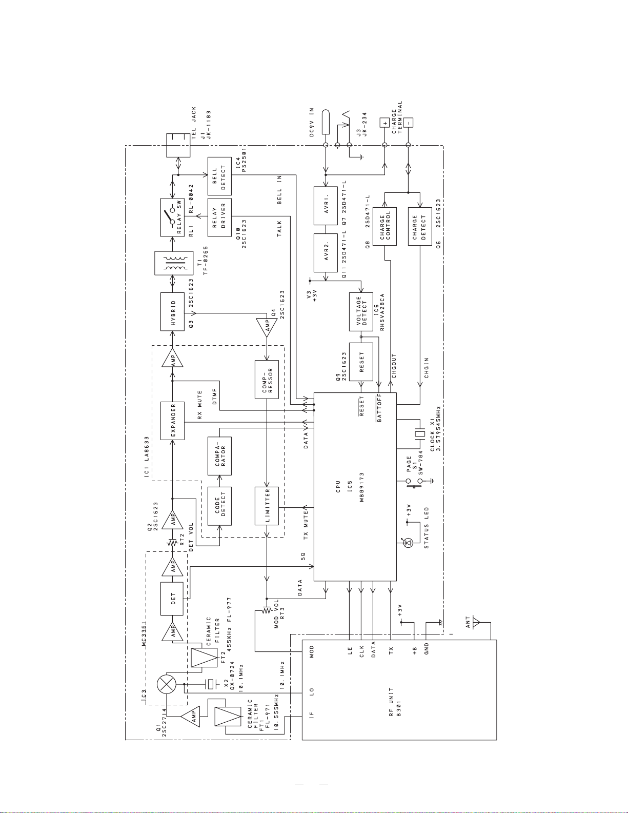
Base Unit
BLOCK DIAGRAMS
7
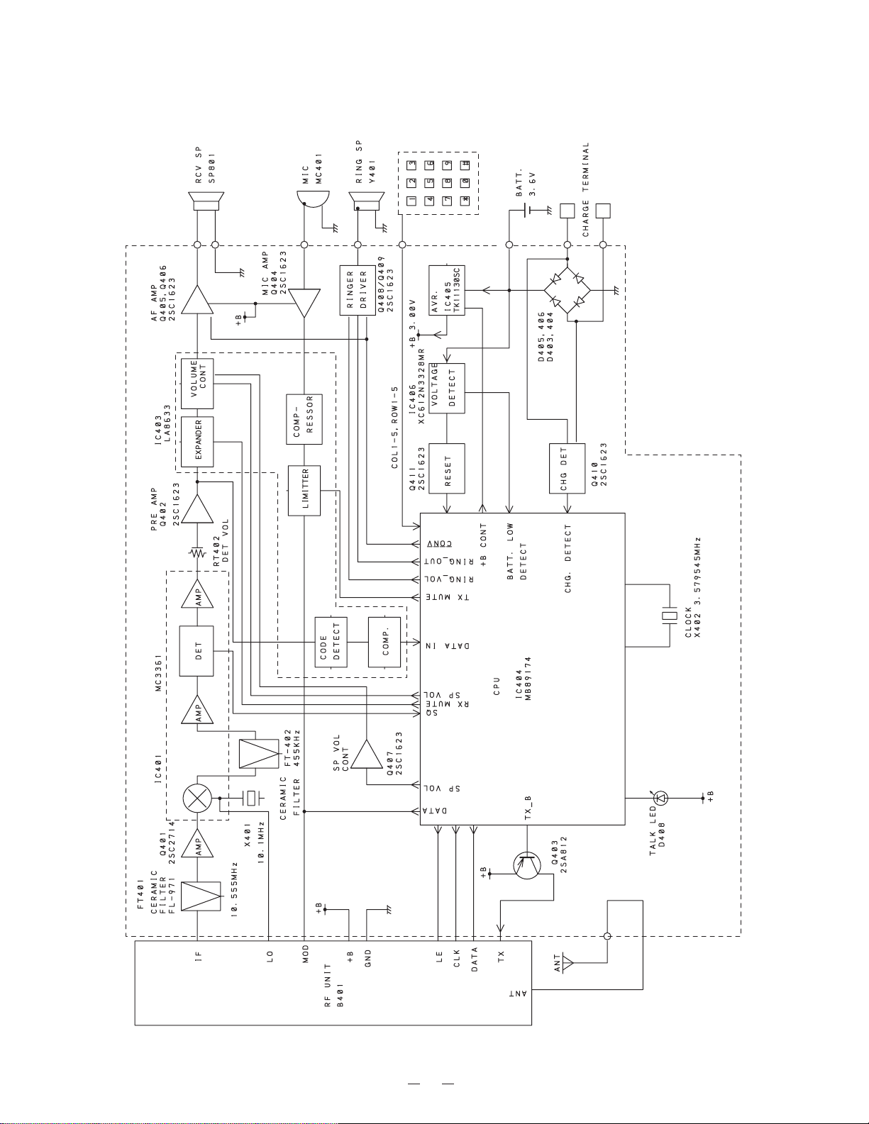
Handset
8
Base Unit
SCHEMATIC DIAGRAMS
9
10
Handset
11
12
TROUBLESHOOTING HINTS
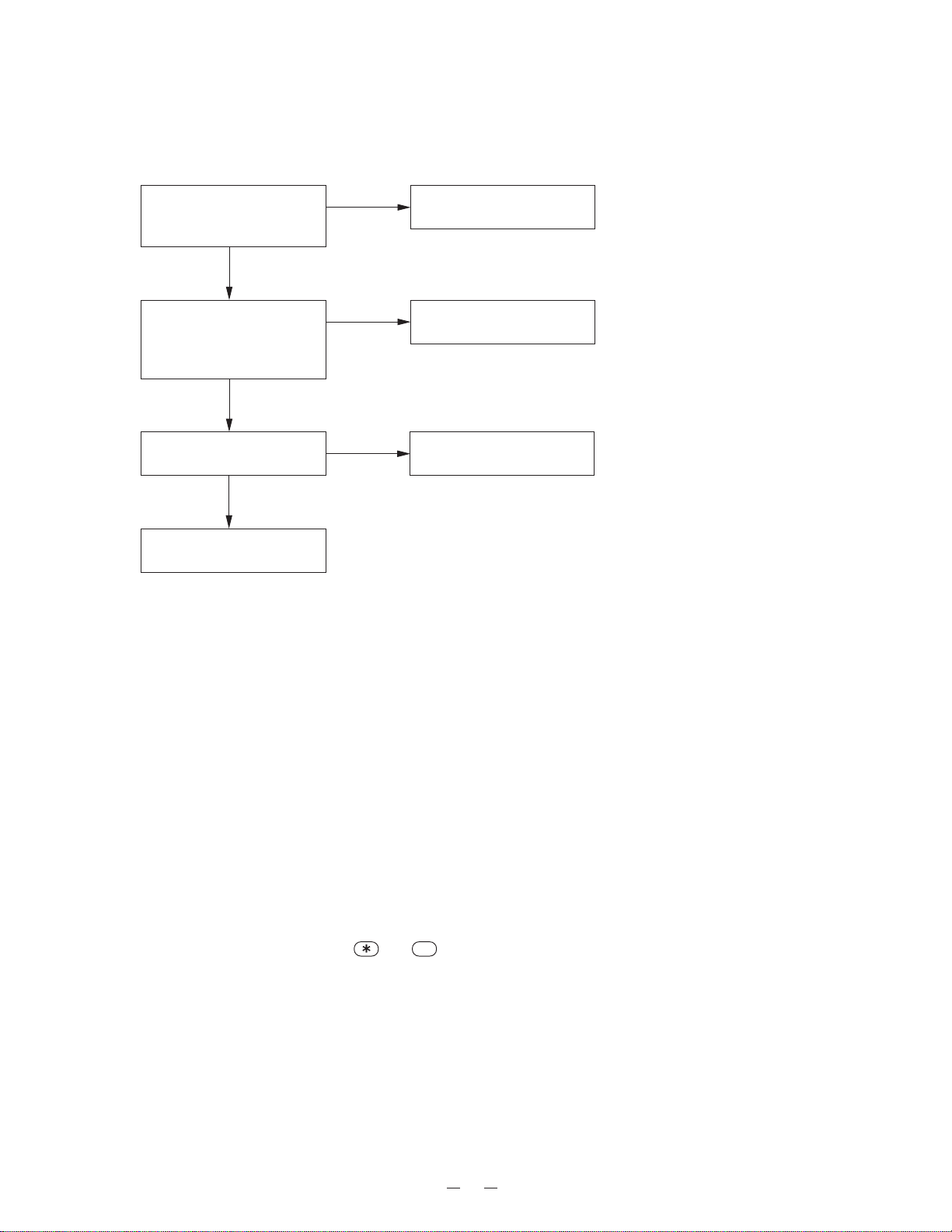
1. The bell does not ring.
When the PAGE SW of the
base is pressed, does the
ringer on the handset ring?
When the TEL SG is joined
with the base to make bell
signal, is there pulse wave at
pin 4 of IC4?
Is there pulse wave at
pin 21 of IC5?
Check IC5 and its
peripheral circuit.
BASE UNIT
OK
OK
OK
NG
NG
NG
See 2. The bell does not ring
& page does not ring.
Check IC4 and TEL network
circuit.
Check R58, C45 and R59.
If you want to reset the unit to the factory settings
1) Set the T/P s witch to TONE position.
2) Diconnect the AC adaptor and telephone line code from the base.
3) While pressing the “PAGE” key, plug the AC adaptor.
Keep pressing the “PAGE” key for about 3 seconds.
4) Keep pressing the “PAGE” k ey, then the IN USE LED will light and the base unit will be reset.
HANDSET
Delection of the Caller ID memory
To delete the Caller ID memory in the EEPROM, proceed with the folloing process:
1) Diconnect the battery from the connector.
2) Connect the battery with pressing and # buttons, and keep pressing the buttons continuously for about
3 seconds.
3) Keep pressing the buttones, and a beep tone will sound and TALK LED will light.
4) Press the “MEM” key, then the handset unit will be reset.
13
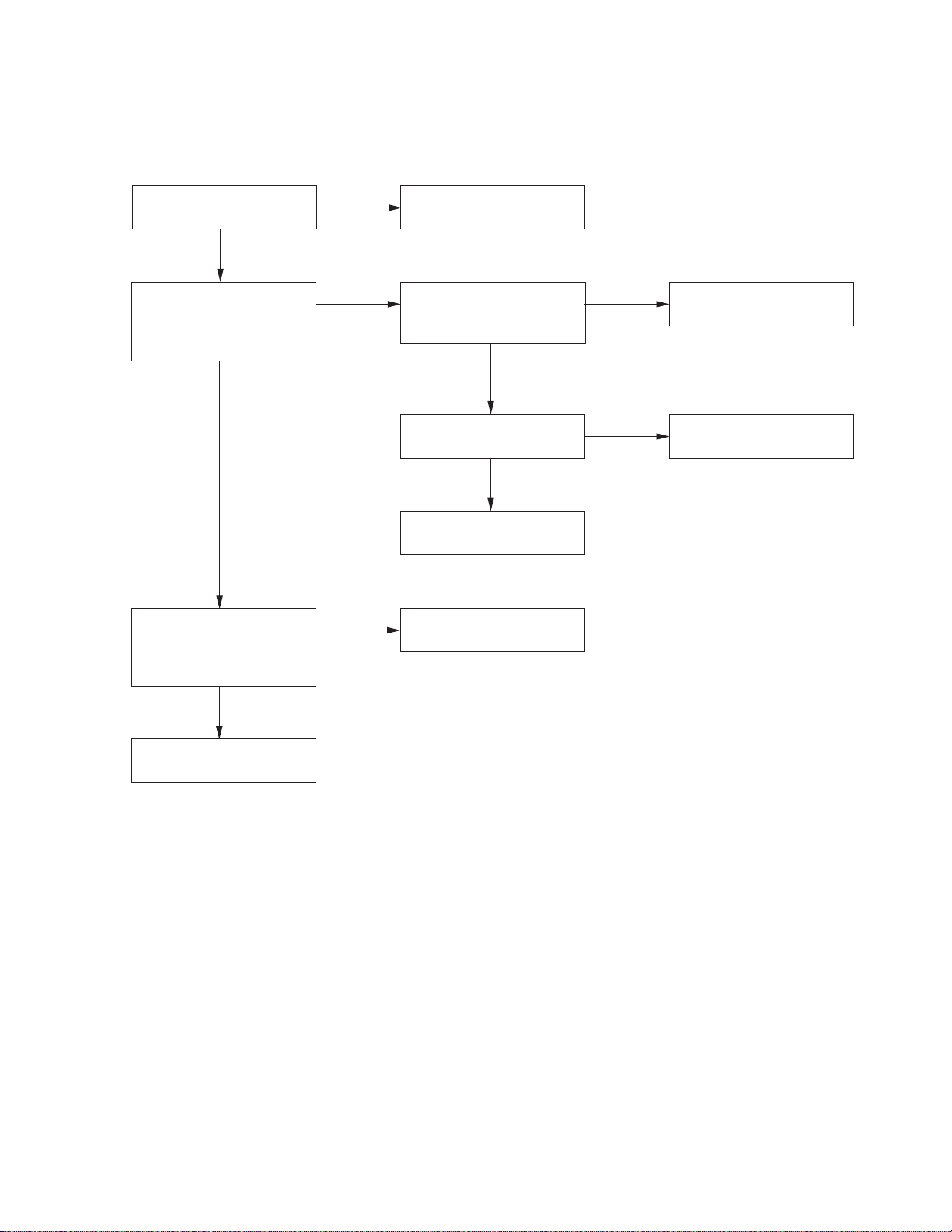
2. The bell does not ring & page does not ring.
Can the base and handset be
connected?
OK
Press handset DIAL key
while in TALK MODE.
Can key touch sound be
heard from the ringer?
OK
When the PAGE SW of the
base is pressed, does pin20
of IC5 change from high to
low?
NG
NG
NG
See 3. The base and handset
cannot be connected.
When the key of the handset is
pressed, can the pulse output
at pin 38 of IC404 be seen?
OK
At the Q408 collector, can the
pulse wave be seen?
OK
Check RINGER Y401.
Check R55, R77 and S1.
NG
NG
Check IC404.
Check R454, R457 and D402.
OK
Check IC5 and its peripheral
circuit.
14
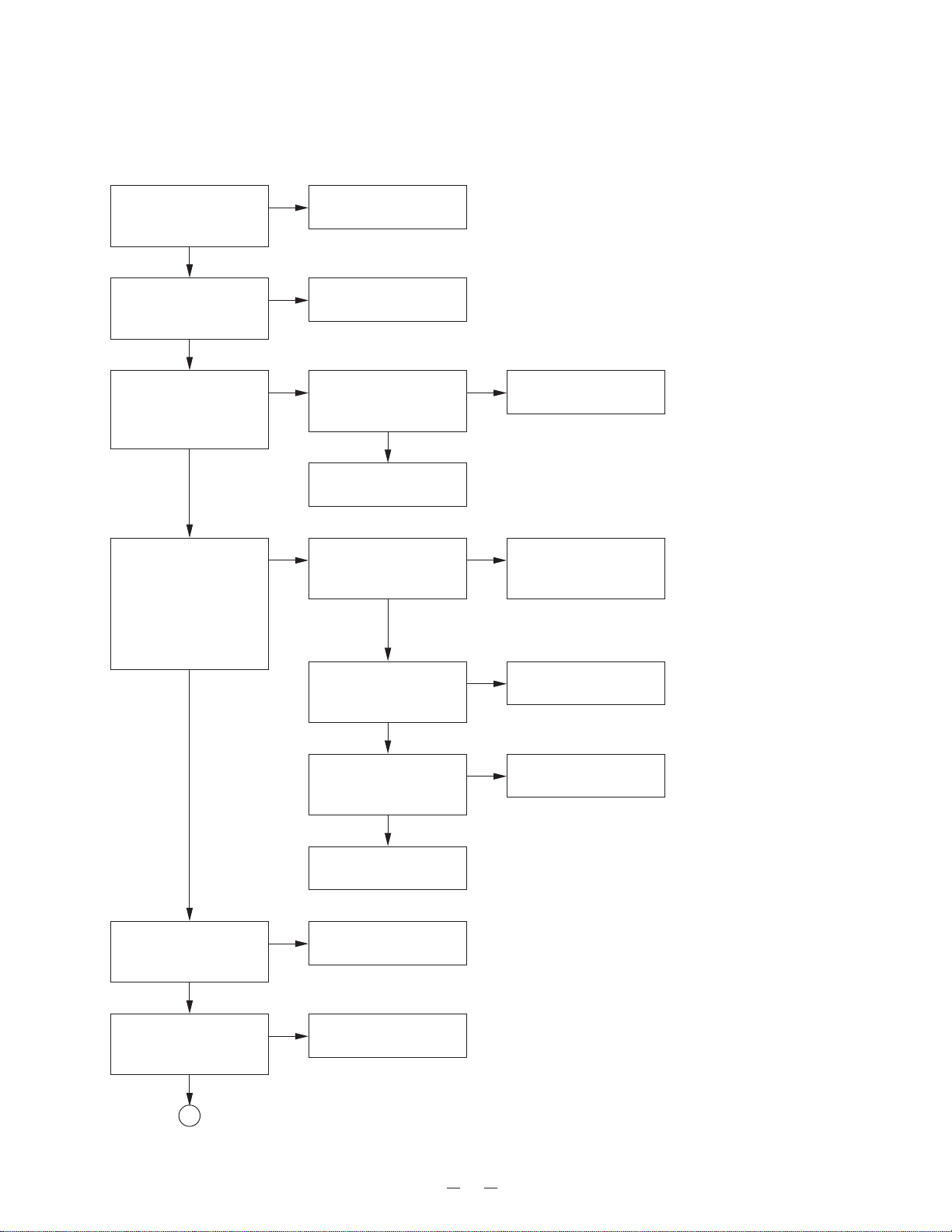
3. The base and handset cannot be connected.
Check whether the base
is able to set in the test
mode 1.
OK
Check the TX POWER
and the TX FREQUENCY
on the base unit.
OK
Press the “PAGE” key 2
times, check whether
deviation of the TX data
is app. 8 kHz Dev.
OK
Press the “PAGE” key 5
times, 902.952467 MHz
(250 Hz ±8 kHz Dev.)
1mV output signal from
RF jack is applied.
Can the IN USE LED be
lighted?
OK
NGACheck IC5 and its
peripheral circuit.
NG
Check base RF unit.
Check whether there is a
NG
250 Hz data wav eform at
“MOD” of RF unit.
OK
Check base RF unit.
NG Check whether there is a
250 Hz data wav eform at
pin 9 of IC3.
OK
Check whether there is a
250 Hz data wav eform at
the Q2 collector.
OK
Check RT3, R40, R68,
NG
R69, R53, R70 and C79.
Check base RF unit and
NG
the peripheral circuit of
IC3.
Check RT2, Q2 and their
NG
peripheral circuit.
Check whether the
handset is able to set in
the test mode 1.
OK
Check the TX POWER
and the TX FREQUENCY
on the handset unit.
OK
Check whether there is a
250 Hz data wav eform at
pin 38 of IC5.
OK
Check IC5 and its
peripheral circuit.
NG Check IC404 and its
peripheral circuit.
NG
Check handset RF unit.
15
Check R42, R46, IC1 and
NG
their peripheral circuit.
 Loading...