

Page 1

2.%&(,"3((456789:;
'&#-.!&(/0,10%
!"#$%&''()&%&*+",&
FT-7007LR
FT-7007LBR
PUBLISHED IN JAPAN, Nov., 1998
Page 2

CONTENTS
SAFETY PRECAUTIONS ............................................................................................................ 1
OPERATING CONTROLS........................................................................................................... 2
ALIGNMENT PROCEDURE ........................................................................................................ 3
BLOCK DIAGRAMS.....................................................................................................................7
SCHEMATIC DIAGRAMS............................................................................................................9
TROUBLESHOOTING HINTS ................................................................................................... 13
IC AND TRANSISTOR VOLTAGE CHART ............................................................................... 20
SEMICONDUCTOR LEAD IDENTIFICATION........................................................................... 24
ELECTRICAL PARTS LOCATION............................................................................................. 26
WIRING DIAGRAM.................................................................................................................... 27
EXPLODED VIEW AND MECHANICAL PARTS LIST............................................................... 28
PARTS LIST............................................................................................................................... 32
ASSEMBLY PARTS LIST .......................................................................................................... 40
SPECIFICATIONS ..................................................................................................................... 41
SAFETY PRECAUTIONS
Before returning any models to the customer, a safety check of the entire instrument should be made. The service
technician must be sure that no protective device built into the instrument by the manufacture has become defective
or inadvertently degraded during servicing.
1.WARNING:
Alterations of the design or circuitry of these models should not be made.
Any design changes or additions such as, but not limited to, circuit modifications, auxiliary speaker jacks, switches,
grounding, active or passive circuitry, etc. may alter the safety characteristics of these models and potentially
create a hazardous situation for the user.
Any design alterations or additions will void the manufacturer's warranty and will further relieve the manufacturer of
responsibility for personal injury or property damage resulting therefrom.
2.PRODUCT SAFETY NOTICE
Many electrical and mechanical parts in this chassis have special characteristics. These characteristics often pass
unnoticed and the protection afforded by them cannot necessarily be obtained by using replacement components
rated for higher voltage, wattage, etc. Replacement parts that have these special safety characteristics are identified
in this manual and its supplements; electrical components having such features are indentified by a in the
schematic diagram and the parts list. Before replacing any of these components, read the parts list in this manual
carefully. The use of substitute replacement parts that do not have the same safety characteristics as specified in
the parts list may create shock, fire or other hazards.
1
Page 3
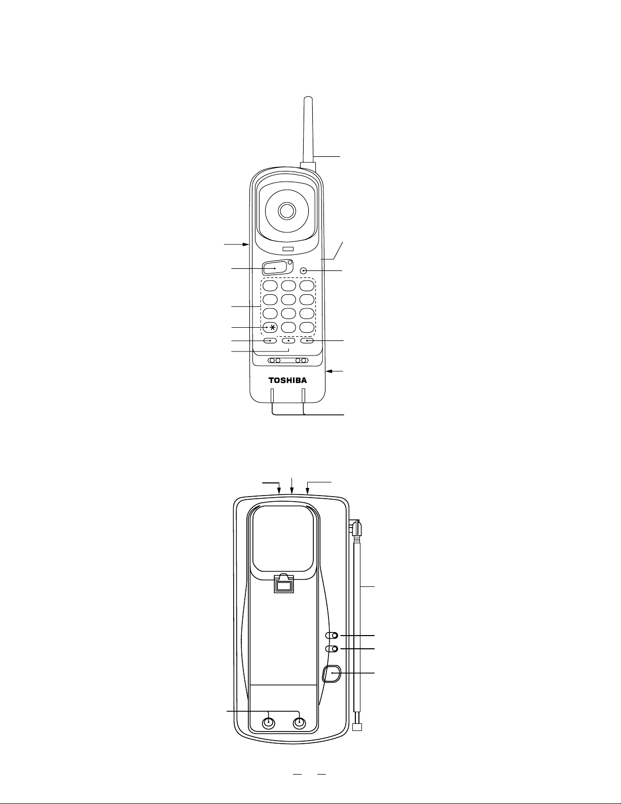
OPERATING CONTROLS
HANDSET CONTROLS AND FUNCTIONS
Speed Dial Index Card(back)
Write all your memorized telephone
numbers.
TALK Button
0-9, æ, # Buttons
TONE
MEM Button
FLASH Button
GHI
PQ
RS
TONE
MEM
1
4
7
TALK
CHANNEL
ABC3DEF
2
JKL6MNO
5
TUV
8
OPER
0
FLASH RDL/P
25
CHANNEL
WX
YZ
/BATT
9
#
Helical Antenna
TALK/BATT.LOW LED
CHANNEL Button
REDIAL/PAUSE Button
Rechargeable Battery Pack
(back)
BASE UNIT CONTROLS AND FUNCTIONS
DC in 9V Jack
Telephone Modular Jack
Charging Contacts
T-P(T ONE-PULSE) Switch
CHARGE
POWER
PAGE
25CHANNEL
COMPANDOR
NOISE
REDUCTION
SYSTEM
FT-7007
TOSHIBA
Charging Contacts
Base Antenna
CHARGE LED
POWER LED
PAGE Button
2
Page 4
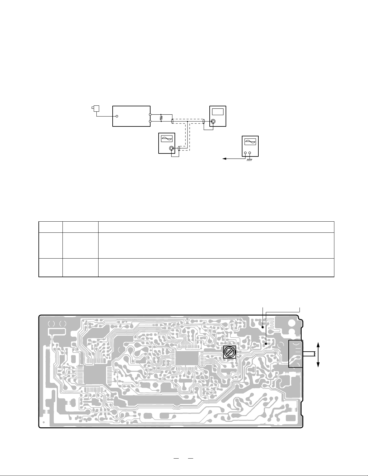
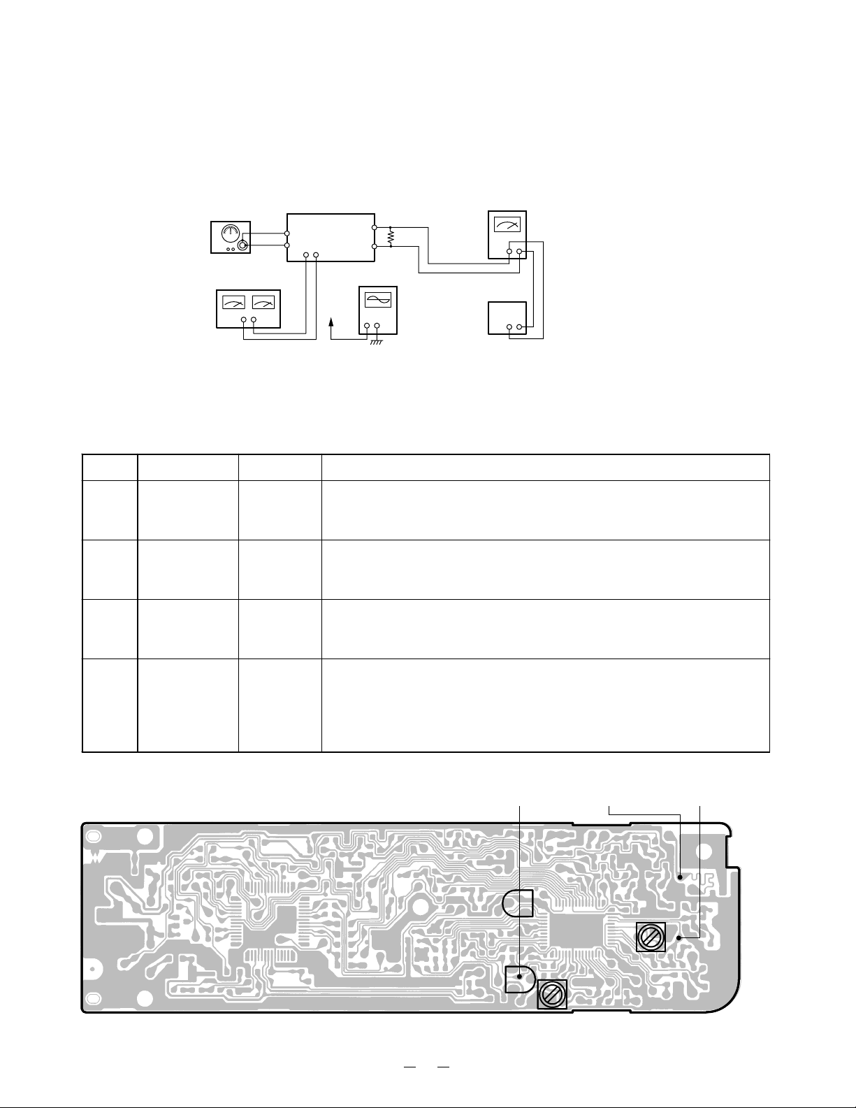
ALIGNMENT PROCEDURE
Base Unit / Transmitter
Test Equipment Required and Connections
• Oscilloscope • Dummy Load, 50-ohm
• Frequency Counter • AC Power Supply : 120V, 60Hz (With AC Adapter)
AC Adapter
(120V 60Hz)
BASE Unit
RF Test
Point
Dummy Load
(50-ohm)
Oscilloscope
Frequency Counter
TX VCO
Test Point
Digital Voltmeter
Preset
a) Set T/P SW to Pulse Mode.
b) Turn on AC power while the Page key is being depressed.
c) Release the Page key 2 seconds later, then the TX Mode is entered (CH21).
Alignment Procedure
Step Adjustment Remarks
Connect the oscilloscope across a 50-ohm load to RF test point.
1L8
Set the digital voltmeter at the test point of TX VCO.
Adjust L8 to indicate DC 2.8V ±0.05V.
2
!
Connect the frequenc y counter across a 50-ohm dummy load to RF test point. Make
sure that the frequency is 46.770 MHz ±1500Hz.
Alignment Point Location on Main PCB
RF Test Point TX VCO Test Point
L8
P
S1
T
T/P SW
3
Page 5
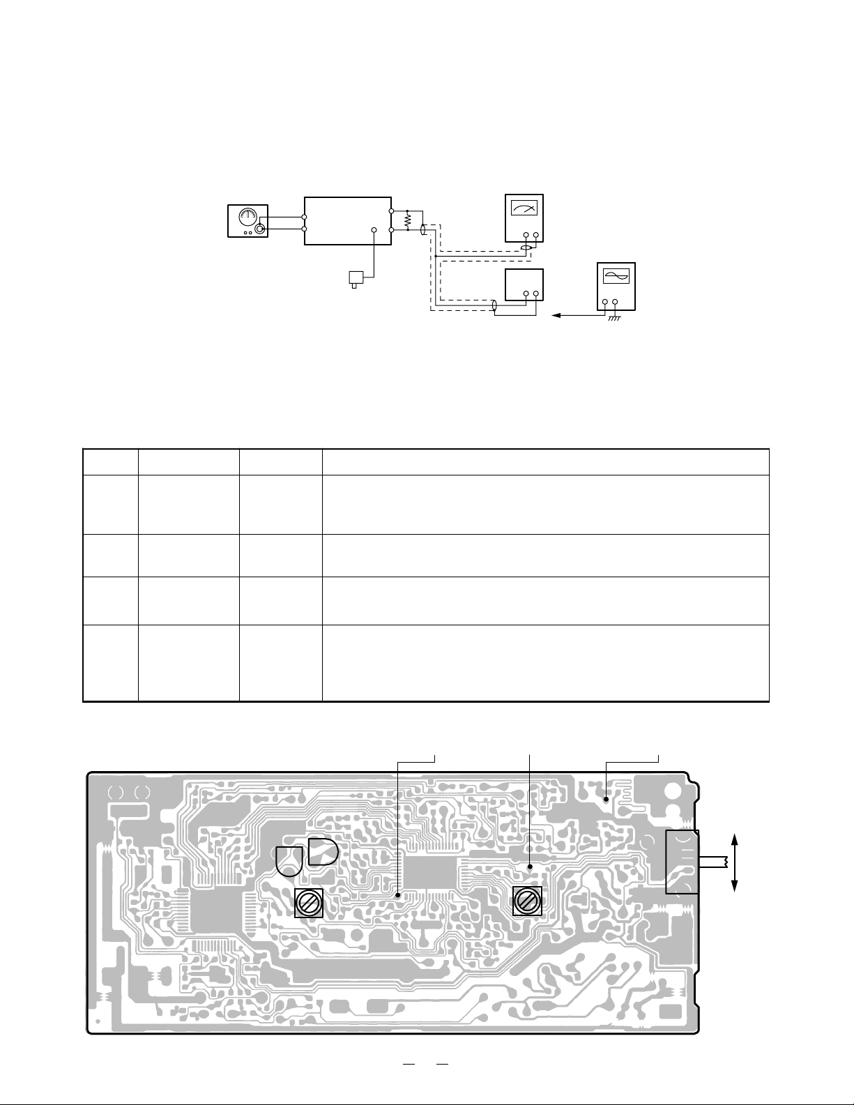
Receiver
Test Equipment Required and Connections
• SG: RF Signal Generator, 49.830MHz • Dummy Load, 600-ohm
• Digital Voltmeter • AF SSVM
• SINAD Meter
Preset
SG
MOD=1kHz
DEV=±3kHz
BASE Unit
RF Test
Point
TEL Jack
AC Adapter
(120V 60Hz)
Dummy Load
(600-ohm)
a) Set T/P SW to Pulse Mode.
b) Turn on AC power while the Page key is being depressed.
c) Release the Page key 2 second later, then the TX Mode is entered (CH21).
d) Press the Page key 4 times, then the DUPLEX Mode is entered (CH21).
Alignment Procedure
Step Preset to Adjustment Remarks
AF SSVM
SINAD
Meter
Digital Voltmeter
Connect the SG to the RF test point.
Connect the digital voltmeter to the test point of the RX VCO.
Adjust L4 to indicate DC 3.3V ±0.05V.
Set the digital voltmeter at the test point of DISCRI.
Adjust L2 to indicate 2.0V ±0.05V.
Connect the AF SSVM to the TEL LINE through a 600- ohm dummy
load, then adjust RT2 to indicate AC -6dBm ±0.5dBm.
1
No modulation
2
No modulation
3
SG: 1mV
SG: 1mV
SG: 1mV
1kHz ±3kHz
deviation
L4
L2
RT2
Press the Page key 2 tim es. Turn RT1 to fully clockwise and co nfir m
4
No modulation
SG: 0.2"V
RT1
the STATUS LED turns off.
Then adjust RT1 to turn to counterclockwise slowly where the STATUS
LED just turns on.
Alignment Point Location on Main PCB
RT2
RT1
L2
DISCRI Test Point RX VCO Test Point
L4
RF Test Point
P
S1
T
T/P SW
4
Page 6
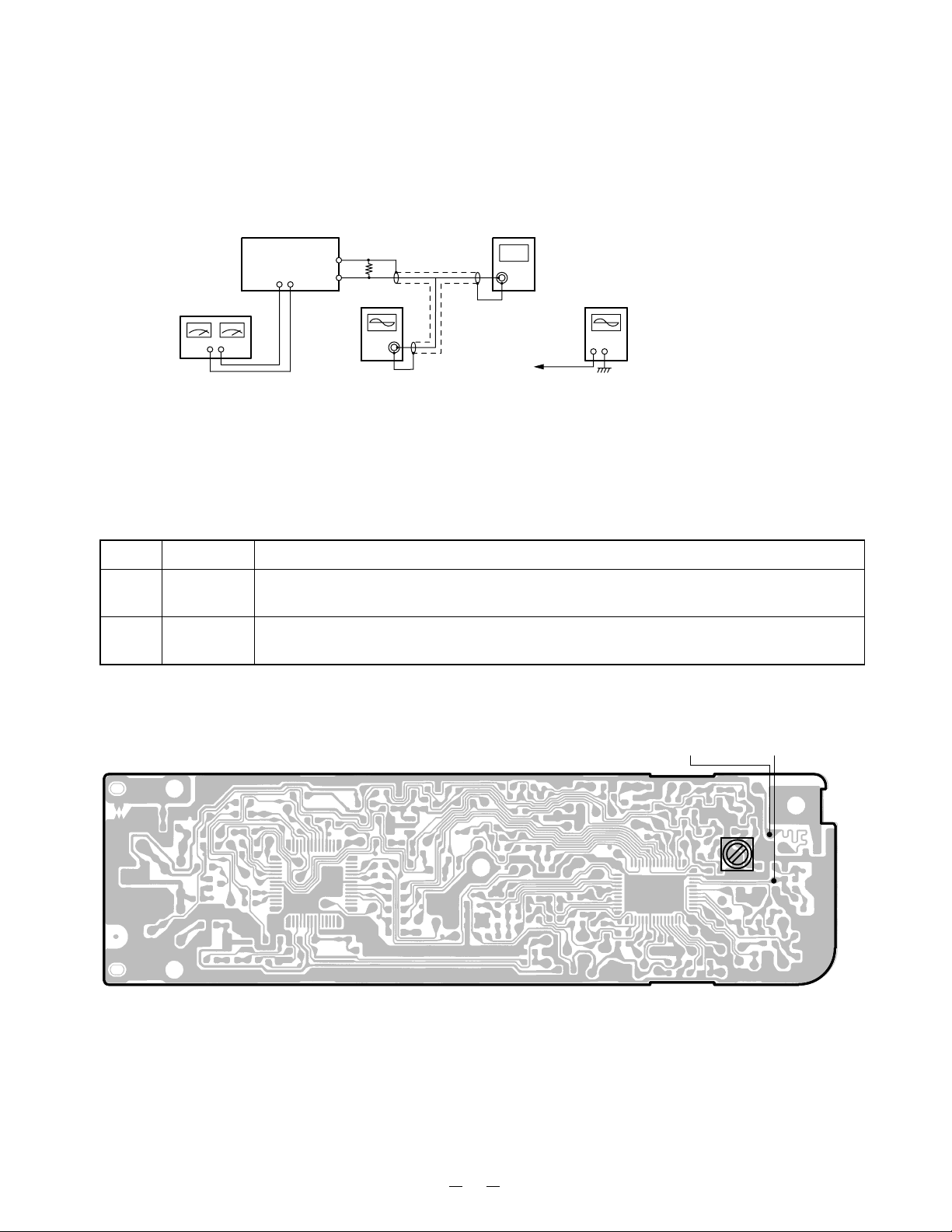
Portable / Transmitter
Test Equipment Required and Connections
• Oscilloscope, 100MHz • Dummy Load, 50-ohm
• Frequency Counter • DC Power Supply, 2.4V
Frequency Counter
Digital Voltmeter
DC Power Supply
2.4V
PORTABLE
Batt Terminal
RF Test
Point
Dummy Load
(50-ohm)
Oscilloscope
Preset
Turn Power On (Connect battery) while depressing " æ" and " # " keys. A beep will be heard. Press the " 1 " key,
then the TX Mode is entered (CH1).
Alignment Procedure
Step Adjustment Remarks
1 L506
2
!
Set the digital voltm eter at the test point of TX VCO, then adjust L50 6 to indicate DC
0.8V ±0.05V.
Connect the frequenc y counter across a 50-ohm dummy load to RF test point. (See
page 25) Make sure that the frequency is 48.760 MHz ±1500Hz.
Alignment Point Location on Main PCB
TX VCO Test PointRF Test Point
L506
5
Page 7
Receiver
Test Equipment Required and Connections
• SG: RF Signal Generator, 46.770MHz • Dummy Load, 150-ohm
• Noise Meter • DC Power Supply: 2.4 V
• Digital Voltmeter • SINAD Meter
SG
MOD=1kHz
DEV=±3kHz
DC Power Supply
2.4V
PORTABLE
RF Test
Point
Batt Terminal
SP
Terminal
Digital Voltmeter
Dummy Load
(150-ohm)
NOISE METER
Balance Input
SINAD
Meter
Preset
Turn Power On (Connect Battery) while depressing "
" and " # " keys. A beep will be heard.
æ
Alignment Procedure
Step Preset to Adjustment Remarks
Press the " 1 " key, then the TX Mode is entered.
Set the digital voltm eter at the test point of RX VCO ( See page 25),
then adjust L503 to indicate DC 2.0 V ±0.05V.
Press the “ 4 ” key, then the RX Adjust Mode is entered.
Connect SG to RF Test Point. Set the digital voltmeter to the DISCRI
Test Point. Adjust L502 to indicate DC 0.9V ±0.05V.
1
No modulation
2
No modulation
SG: 1mV
SG: 1mV
L503
L502
SG: 1mV
3
1kHz ±3kHz
RT502
deviation
Connect the NOISE MET ER to the SP Terminal thr ough a 150-ohm
dummy load, then adjust RT502 to indicate 140 ±5 mV.
Press the “MEMO” key, then the SQ Adjust Mode is entered.
SG: 0.09"V
4
1kHz ±3kHz
RT501
deviation
Connect SG to RF Test Point. Turn RT501 to fully clockwise and
confirm the Ringer SP501 does not r ing.
Adjust RT501 to turn to counter clockwise slowly where the ringer
SP501 rings.
Alignment Point Location Main PCB
DISCRI Test Point
RT502
L502
RT501
RX VCO Test PointRF Test Point
L503
6
Page 8
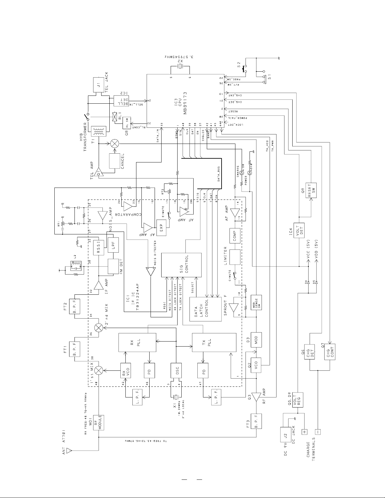
Base Unit
BLOCK DIAGRAMS
7
Page 9
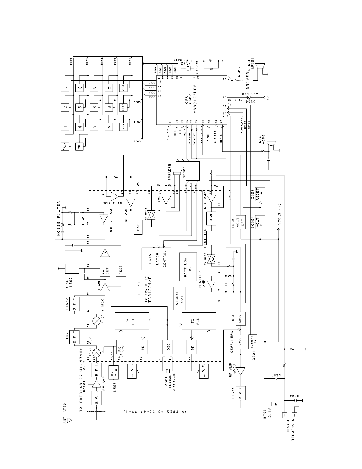
Handset
8
Page 10
DISCRI
TEST POINT
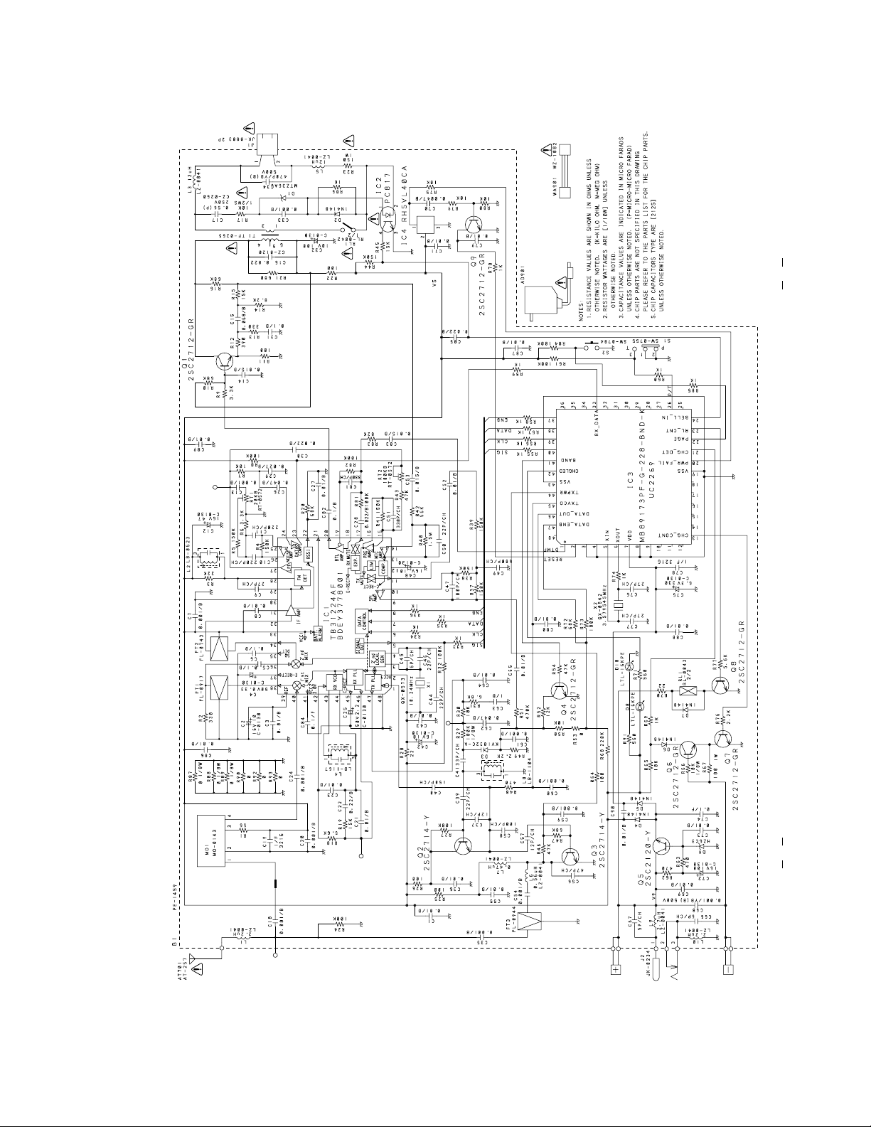
SCHEMATIC DIAGRAMS
10
Base Unit
TX VCO TEST POINT
9
RX VCO
TEST POINT
RF TEST POINT
Page 11
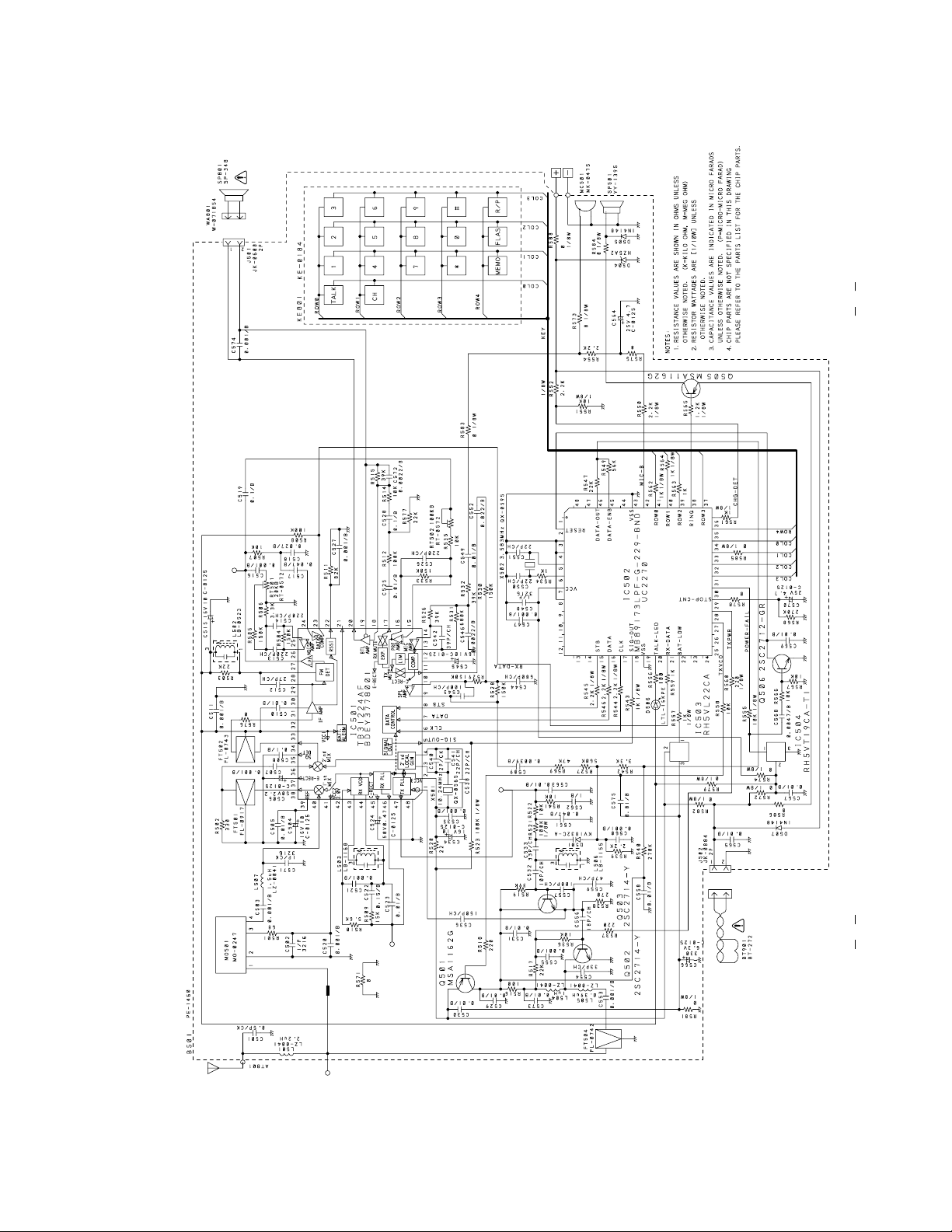
DISCRI
TEST POINT
12
Handset
TX VCO
TEST POINT
11
RX VCO
TEST POINT
RF TEST POINT
Page 12
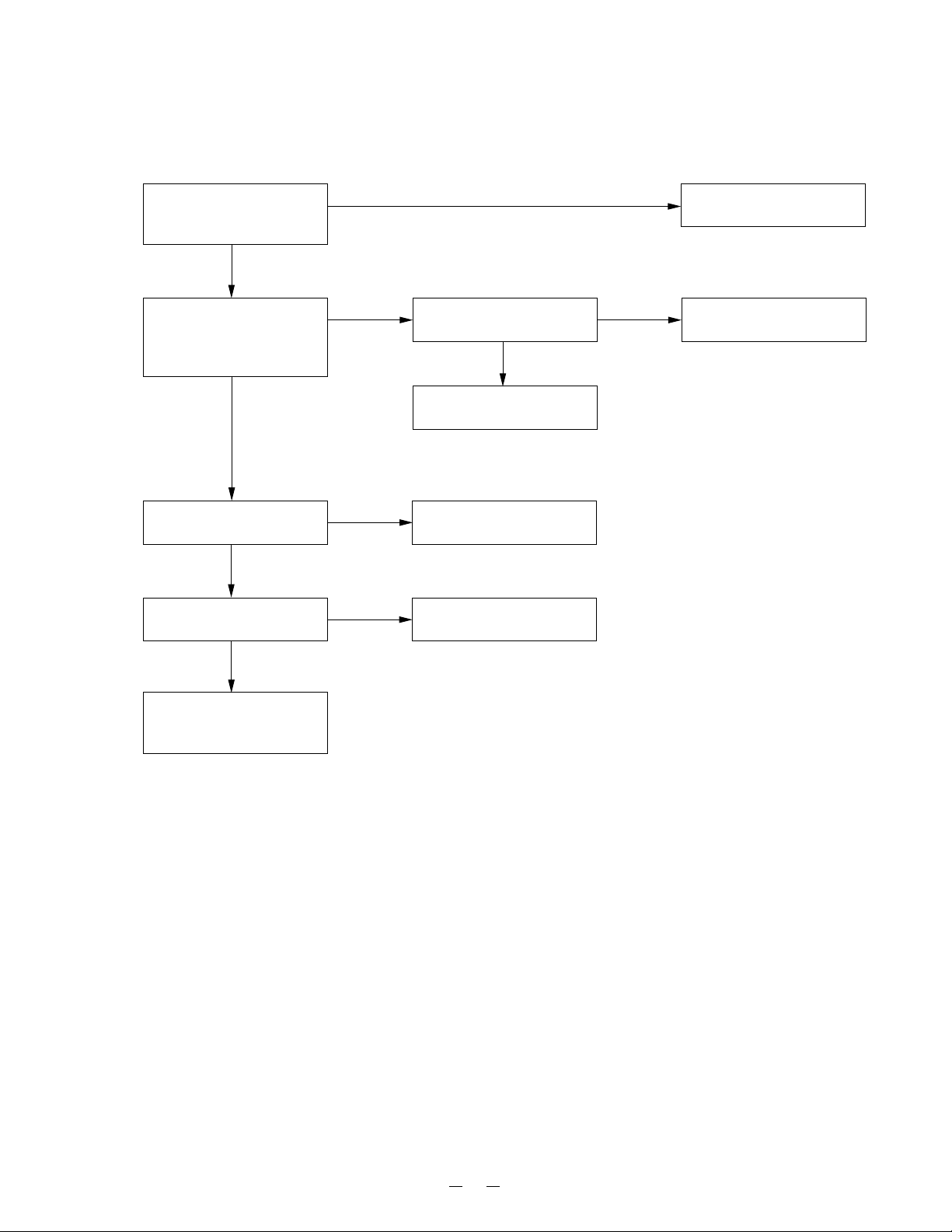
TROUBLESHOOTING HINTS
1. The bell does not ring.
When the PAGE SW of the
base is pressed, does the
ringer on the handset ring?
OK
When the TEL SG is joined
with the base to make bell
signal, is there pulse wave on
Pin 4 of IC2?
OK
Then, is there pulse wave
on Pin 24 of IC3?
OK
By using voltage chart,
check IC3.
OK
NG
NG
NG
NG
By using voltage chart, check
IC2.
OK
Check TEL network primary
circuit.
Check IC3, C85, R45 and
R44.
IC3 is defective.
NG
See 2. The bell does not ring
& page does not ring.
IC2 is defective.
Check the surrounding
circuit where the voltage is
incorrect.
13
Page 13
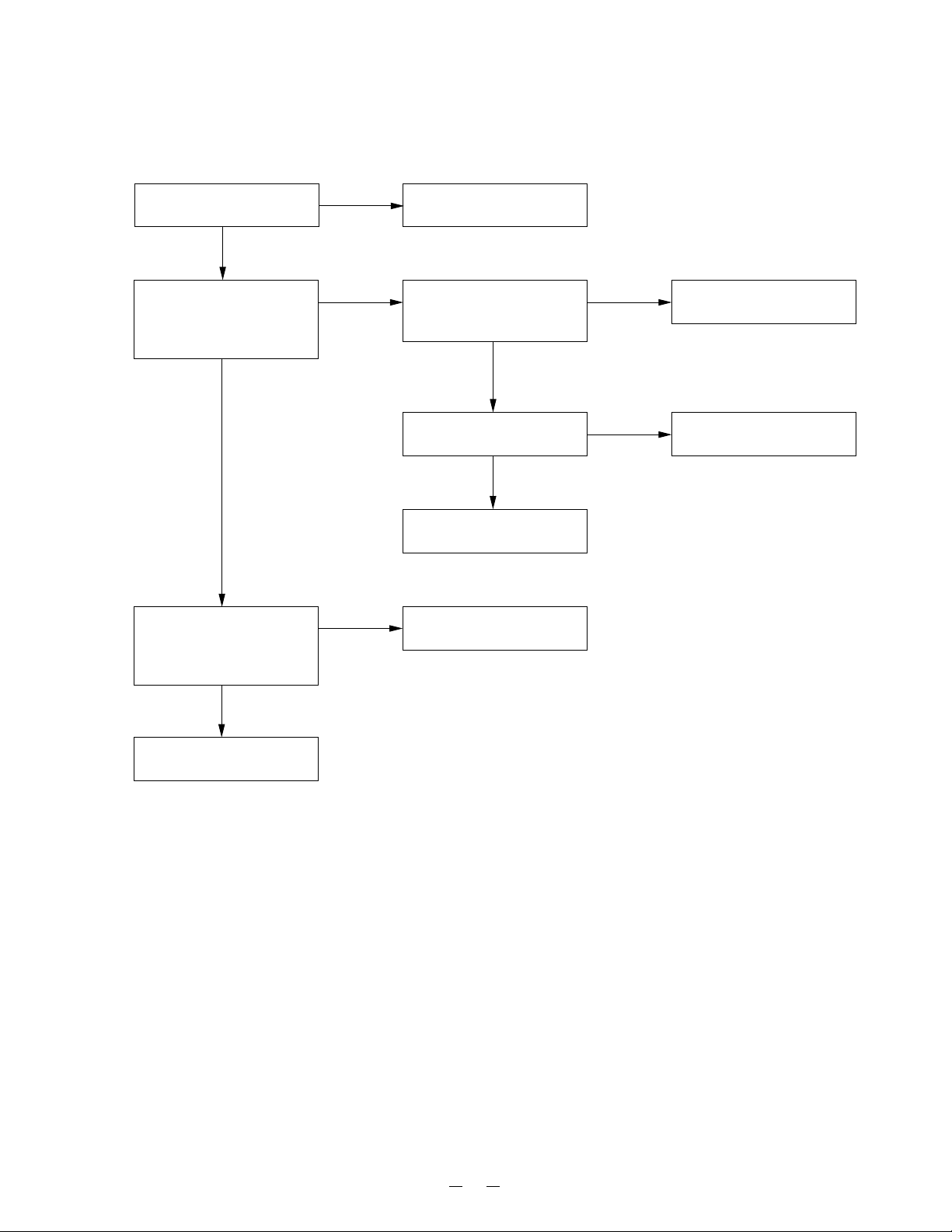
2. The bell does not ring & page does not ring.
Can the base and handset be
connected?
OK
Press handset DIAL key
while in TALK MODE,
can key touch sound be
heard from the ringer?
OK
When the PAGE SW S2 of
the base is pressed, does
pin22 of IC3 change from
high to low?
NG
NG
NG
See 3. The base and handset
cannot be connected.
When the key of the handset is
pressed, can the pulse output
at pin 38 of IC502 be seen?
OK
At the Q505 collector, can the
pulse wave be seen?
OK
Check RINGER SP501.
Check S2, R58 and R73.
NG
NG
Check IC502.
Check R565, R586 and Q505.
OK
Check IC3 and its peripheral
circuit.
14
Page 14

3. The base and handset cannot be connected.
Check whether the base is
able to set in the test mode 1.
OK
Check the TX FREQUENCY
on the base unit.
OK
Check the TX PO WER on the
base unit.
OK
Set the base in the test mode
3. Check whether deviation
of the TX data is app. 8kHz
Dev.
OK
NG
NG
NG
NG NG
Check the power peripheral
circuit, IC3 and its peripheral
circuit.
Check Q2, D3 and their
peripheral circuits.
T ry adjust TX VCO VOL TA GE
again.
Check Q2, Q3, FT3 and their
peripheral circuits.
OK
Check whether there is a
200Hz data wavefor m at pin
46 of IC3.
OK
Check R72, R73, R68, R53,
R50, R49 and C61.
Check IC3.
Set the base in the test mode
6, 49.83MHz (200Hz 8kHz
Dev.) 1mV output signal from
ANT IN is applied.
Can the CHG LED be lighted?
OK
A
NG NG Check MO1, FT1, FT2, L2, L4
Check whether there is a
200Hz data wavefor m at pin
27 of IC1.
OK
Check Whether there is a
200Hz data wavefor m at pin
23 of IC1.
OK
Check whether there is a
200Hz data wavefor m at pin
33 of IC3.
OK
Check IC3 and its peripheral
circuit.
NG
NG
and their peripheral circuits.
Try adjust RX VCO VOLTAGE
and DISCRI V OLTAGE again.
Check R7, C29 and C26.
Check R59.
15
Page 15

A
Check whether the handset is
able to set in the test mode 2.
OK
Check the TX FREQUENCY
on the handset unit.
OK
Check the TX POWER on the
handset unit.
OK
Set the handset in the test
mode 3. Check whether
deviation of the TX data is
app. 5kHz Dev.
OK
NG
NG
NG
NG NG
Check the power peripheral
circuit, IC502 and its peripheral
circuit.
Check Q503, D501 and their
peripheral circuits.
T ry adjust TX VCO V OL T A GE
again.
Check Q503, Q502, FT504
and their peripheral circuits.
Check whether there is a
200Hz data wavefor m at pin
46 of IC502.
OK
Check R547, R549, R540,
R542, R539 and C560.
Check IC502.
Set the handset in the test
mode 10, 46.77MHz (200Hz
5kHz Dev.) 1mV output signal
from ANT IN is applied.
Check whether the bell ring.
OK
Place the handset on the base
to charge about 5 seconds,
then connect again.
NG
Check the charge circuit of
base and handset.
NG NG Check MO501, FT501, FT502,
Check whether there is a
200Hz data waveform at Pin
27 of IC501.
OK
Check whether there is a
200Hz data waveform at Pin
23 of IC501.
OK
Check whether there is a
200Hz data waveform at Pin
21 of IC502.
OK
Check IC502 and its peripheral
circuit.
NG
NG
L503 and their peripheral
circuits.
Try adjust RX VCO VOL TA G E
and DISCRI VOL TAGE again.
Check R507, C518 and C517.
Check R559.
16
Page 16

4. Cannot make a phone call (pulse).
Can the base and handset
be connected?
OK
While in TALK MODE, press
dial key of the handset.
Can pulse feedback be
heard from the handset
speaker?
OK
Check the base TEL-line
network primary circuit.
NG
NG
5. Cannot make a phone call (tone).
Can the base and handset be
connected?
OK
NG
See 3. The base and handset
be cannot be connected.
See 3. The base and
handset cannot connect.
Check the base RELAY
control (around Pin 23 of
IC3).
While in TALK MODE, press
dial key of the handset.
Can tone waveform from Pin
1 of IC3 is fed?
OK
Can tone signal be heard
from the handset speaker?
OK
Check the base TEL-line
circuit and RELAY control
circuit.
NG
NG
Check IC3.
Check Pin 18~20 of IC1, Q1
and their peripheral circuits.
17
Page 17

6. Voice cannot be transmitted to other party (outgoing call).
Can the base and handset be
connected?
OK
Does the bias voltage exitst
at MC501?
OK
The 1kHz 18mV sine wavef orm
is applied to MC501 +side, can
the 1kHz sine wave form Pin13
of IC501 be fed?
OK
Check whether there is the sine
wave f orm at Pin9 of IC501.
OK
TX output signal from the
handset is detected by the liner
detector, can the 1kHz 3kHz
Dev. sine waveform be fed.
OK
NG
NG
NG
NG
NG
See 3. The base and handset
be cannot be connected.
Check R573, R554, R575,
R550 and C564.
Check IC501 and Pin13~14
peripheral circuits of IC501.
Check IC501 and Pin 9~11
peripheral circuits of IC501.
Check C509, R569 and R527.
Check Whether there is the
1kHz sine waveform at Pin16
of IC1.
OK
Check whether there is the
1kHz sine waveform at Pin20
of IC1.
OK
Check whether there is the
1kHz sine wavefor m at the
Q1 collector.
OK
Check whether the 1kHz sine
waveform from TEL-line
output is fed.
OK
Check MC601 of handset.
NG
NG
NG
NG
Check IC1 and Pin15~16
peripheral circuits of IC1.
Check IC1 and Pin17~20
peripheral circuits of IC1.
Check Q1 and its peripheral
circuit.
Check T1, RL1 and their
peripheral circuits.
18
Page 18

7. The voice of the caller cannot be heard (incoming call).
Can the base and handset be
connected?
OK
The 1kHz 97.5mV sine
wavefor m is applied to
TEL-line of the base, can the
1kHz sine waveform from
the Q1 collector be fed?
OK
Check whether there is the
1kHz sine wavef orm at Pin13
of IC1.
OK
Check whether there is the
1kHz sine wavefor m at Pin9
of IC1.
OK
TX output signal from the
base is detected by the liner
detector, can the 1kHz 3kHz
Dev. sine waveform be fed?
OK
NG
NG
NG
NG
NG
See 3. The base and handset
be cannot be connected.
Check the base TEL-line circuit
and RELAY control circuit.
Check IC1 and Pin13~14
peripheral circuits of IC1.
Check IC1 and Pin9~11
peripheral circuits of IC1.
Check C65 and R51.
Check whether there is the
1kHz sine wavef orm at Pin16
of IC501.
OK
Check whether there is the
1kHz sine wavef orm at Pin19
and 20 of IC501.
OK
Check whether there is the
1kHz sine waveform dur ing
for Pin1 and 2 of J501.
OK
Check SP801 and WA801.
NG
NG
NG
Check IC501 and Pin15~16
peripheral circuits of IC501.
Check IC501 and Pin17~20
peripheral circuits of IC501.
Check J501 and its soldering.
19
Page 19

IC AND TRANSISTOR VOLTAGE CHART
Base Unit Unit[V] Unit[V]
Ref. No PIN STBY TALK NOTE
1 Vcc 5-4.9 Sine wave
2Vcc 4.9
3 Vcc-4 CLOCK 10.24MHz
4 Vcc-4 CLOCK 10.24MHz
5 Vcc-GND Vcc-GND Pulse
6 Vcc-GND Vcc-GND Pulse
7 Vcc-GND Vcc-GND Pulse
8 Vcc-GND Vcc-GND Pulse
9 GND 2-1 Sine wave
10 GND 1.5
11 1.2 2 -1 S ine wav e
12 1.1 1.5
13 1.0 2-1 Sine wave
14 0.7 1.5
15 1.0-GND 1.5
16 1.0-GND 2-1 Sine wave
17 GND 1.5 Sine wa ve
18 1.2 1.3
19 1.2 1.3 Sine wave
20 1.2 1.3 Sine wave
21 GND GND
IC1 22 0.5 1.5
23 Vcc-GND Vcc-GND Pulse
24 1-0.6 0.8 Sine wave
25 0.7 0.8
26 0.7 0.8
27 2-GND 1.0 Sine wave
28 2.8-2.4 Vcc-4.5 Sine wave
29 4-3.8 4.2-3.8 Sine wave
30 GND GND
31 4.9 4.5
32 4.9 4.6-4.4 Sine wave
33 4.9 Vcc
34 3.5 3.6-3.4 Sine wave
35 1.2-1.0 GND
36 1.0 1.0
37 0.1 0.7
38 3.5 3.5-3.4 Sine wave
39 0.5 1.5
40 1 1
41 2.0 2
42 4-3.5 3.8
43 5-4.8 Vcc -4.8 Sine wa ve
44 Vcc Vcc
Ref. No PIN STBY TALK NOTE
45 0.5 0.8
IC1
IC2
IC3
46 Vcc-4 3.8
47 GND 1.4
48 GND GND
1 OPEN OPEN Sine wave
2 OPEN OPEN Sine wave
3GND GND
4Vcc GND
1GND GND
2Vcc Vcc
3GND GND
4GND GND
5 3.8-GND 3.8-GND Clock
6 Vcc-GND Vcc-GND Clock
7Vcc Vcc
8GND GND
9GND GND
10 GND GND NC
11 GND GND NC
12 GND GND
13 Vcc 4.8
14 GND GND NC
15 GND GND NC
16 GND GND NC
17 GND GND NC
18 GND GND NC
19 GND GND GND
20 Vcc Vcc
21 Vcc Vcc
22 Vcc Vcc PAGE
23 GND Vcc RL CONT
24 GND Vcc BELL IN
25 GND GND NC
26 GND GND P/T
27 GND GND NC
28 GND GND NC
29 GND GND NC
30 GND GND NC
31 GND GND NC
32 GND GND NC
33 Vcc-GND Vcc-GND Pulse
34 GND GND NC
35 GND GND NC
36 GND GND NC
POWER FAIL
CHAGE DET
20
Page 20

Unit[V]
Ref. No PIN STBY TALK NOTE
37 Vcc-GND Vcc-GND Pulse
38 Vcc-GND Vcc-GND Pulse
39 Vcc-GND Vcc-GND Pulse
40 Vcc-GND Vcc-GND Pulse
41 Vcc-GND Vcc BAND
IC3
IC4
Q2
Q4
Q6
Q8
42 Vcc GND CHGLED
43 GND GND Vss
44 GND 3.0 TXPWER
45 GND GND TXVCO
46 GND GND DATA OUT
47 GND GND DATA ENB
48 GND GND NC
1Vcc Vcc
2Vcc Vcc
3GND GND
E1.8 1.0
C GND 4-3 Sine waveQ1
B 1.0 1.8 Sine wa ve
E 4.4 2- 1.5 Sine wave
CVcc 4.5
B GND 2.5-2 Sine wave
EGND GND
C Vcc Vcc-3.5 Sine waveQ3
BGND 0.8
E0.6-GND GND
CGND GND
BGND 0.6
E5.6 5.6
C 10-9 9-8 Sine waveQ5
B6.3 6.3
EGND GND
CVcc Vcc
BGND GND
E0.8 GND
CGND GNDQ7
BGND 0.8
EGND GND
C 10-9 0.1
BGND 0.8
EGND GND
CVcc VccQ9
BGND GND
21
Page 21

Handset Unit[V] Unit[V]
!"#$%&'$ ()& *+,- +./0 &1+2
34$5 4$5
4 4$5 4$5 6778
8 39$4:;<= 39$4:;<= >?'7@
: 39$4:;<= 39$4:;<= >?'7@
A 9B4$5 9B4$5 (C?D"
5 9B4$5 9B4$5 (C?D"
E 9B4$5 9B4$5 (C?D"
F 9B4$5 9B4$5 (C?D"
G9 3$4
39 9 3$4
33 3$3 3 $4
34 9 3$4
38 3$3 3$4
3: 3$3 3$4
3A 9B9$8 3$4
35 9B9$8 3$4
3E 9 3$4
3F 9 3$4
3G 9 3$4
49 9 3$3
43 9 9
)>A93
44 9 3$A
48 9B4$5 9B4$5 (C?D"
4: 9B9$5 9$5 (C?D"
4A 9B9$5 9$5 (C?D"
45 9B9$5 9$5 (C?D"
4E 9B9$5 9$E (C?D"
4F 4$5H4$AB8$9I 4$5
4G 4$3H3$AB4$3I 3$AB3$F *JK"%LMN"
89 9 9 O&P
83 4$4B4$5 4$4 (C?D"
84 4$4B4$5 3$FB4$A *JK"%LMN"
88 4$5 4$5 6773
8: 3$:B3$E 3B3$E *JK"%LMN"
8A 9B9$A 9 (C?D"
85 9B9$F 9$FB3$9 *JK"%LMN"
8E 9 9$E
8F 3$3B3$E 9$FB3$8 *JK"%LMN"
8G 9 3$4
:9 9B9$F 3$3 (C?D"
:3 9$4B4$9 4$9 6774
:4 9 4$9
:8 9 4$AB4$E *JK"%LMN"
:: 9 4$A
!"#$%&'$ ()& *+,- +./0 &1+2
:A 9 9$5
)>A93
)>A94
:5 9 3$G
:E 9 9$G
:F 9 9 O&P
39 9 &>
4 4$5 4$A !2*2+
89 9
:9 9
A 9B4$9 9B3$F 1*>
5 9B4$5 9B4$5 1*>
E4$5 4$5 677
F9 9
G9 9 &>
39 9 9 &>
33 9 9 & >
34 9 9 &>
38 9 4$5 &>
3: 9 9 &>
3A 9B4$5 9B4$5 (C?D"
35 9B4$5 9B4$5 (C?D"
3E 9B4$5 9B4$5 (C?D"
3F 4$5 9B4$5 (C?D"
3G 9 9 (C?D"
49 3$3B4$5 9 +./0B/2P
43 9B4$5 9B4$5 !QBP.+.
44 4$5 4$5 ,.+B/1R
48 9 9 &>
4: 9 9 &>
4A 9 9 &>
45 9 9 &>
4E 4$4B4$5 9 +QB6>1
4F 9B9$A 3$3 +QB(R!
4G 9$AB4$5 4$:
89 4$5 4$A
83 4$5 4$A >1/8
84 4$5 4$A >1/4
88 4$5 4$A >1/3
8: 4$5 4$A >1/9
8A 9 9 !1R:
85 9 9 ><OBP2+
8E 9 9 !1R8
8F 4$9B4$5 4$A !)&O
8G 9 9 !1R4
:9 9 9 !1R3
*+1(B>1&+
(1R2!BS.)/
22
Page 22

Unit[V]
Ref. No. PIN STBY TALK NOTE
41 0 0 ROW0
42 0 2.5 MIC-B
43 0 0 GND
IC502
IC503
IC504
Q501
Q502
Q503
Q505
Q506
44 0 0 RINGVOL
45 0 0 DATA-ENB
46 0 0 DATA-OUT
47 0 0 NC
48 0 0 NC
12.6 2.6 OUT
22.6 2.6 Vcc
30 0 GND
12.6 2.6 OUT
22.6 2.6 Vcc
30 0 GND
E2.6 2.6
C0 2.6
B2.0-2.6 2.0
E0 0 GND
C 0 1.7-2. 6 Sine wa ve
B 0 0.5-0.8 Sine wave
E 0 0.5-1.1 Sine wave
C0-2.6 2.6
B 0-1.5 1.4-1.8 Sine wave
E2.6 2.6
C0 0
B 2.1-2.6 2.6 RING
E0 0 GND
C2.6 2.6
B0 0
23
Page 23

Base Unit
SEMICONDUCTOR LEAD IDENTIFICATION
D1:MTZ36AJ
D2 / D4 /
D5 / D6 / D7 : 1N4148
D9 :HZ6C3
Anode
Q5 : 2SC2120
E
C
B
IC1
GND248
TB31224AF
TX-OUT47
Cathode
RX-OUT46
C-RECT45
D3 : KV1832C
Anode
D8 / D10 : LTL-16KPE-A
Anode
CC241
REF39
1st MIX-IN40
VCO244
VCO143
V
VCO-CONT42
V
Cathode
Cathode
Q1 / Q4 / Q6 / Q7 / Q8 / Q9 : 2SC2712
Q2 / Q3 : 2SC2714
IC3
MB89173PF
B
E
B : Base
E : Emitter
C : Collector
C
P4048
P4147
P4246
P4345
P4444
Vss43
P30 / SDK42
P31 / S041
P32 / S140
P33 / EC39
P34 / TO / INT038
P35 / INT137
1TX-IN
CC3
C-NF
MIC-OUT
MIC-IN
2V
3LO1
4LO2
5SIG-OUT
6CLK
7DATA
8STB
9FIL-OUT
10FIL-IN
11COMP-OUT
12
13
14
15PRE-IN
16PRE-OUT
17EXP-OUT
18RECE-IN
19RO1
IC2
PC817
1
23
4
20RO2
21BAT-ALM
27
26
25
22RSSI
23D-COMP-OUT
24D-COMP-IN
1st MIX-OUT38
E-RECT37
2nd MIX-IN36
N-REC35
2nd MIX-OUT34
CC133
V
IF-IN32
DEC31
GND130
IF-OUT29
QUAD28
AF-OUT
N-FIL-OUT
N-FIL-IN
IC4
PH5VL40CA
1DTMF
2RST
3MDD0
4MDD1
5X0
6X1
7Vcc
8P50 / (X0A)
9P51(Z1A)
10P27
11P26
12P25
13P24
14P23
15P22
16P21
17P20
18P17
19Vss
20P16
21P15
22P14
23P13
24P12
3
2
1
P36 / INT236
P37 / BZ35
P00 / L1034
P01 / L1133
P02 / L1232
P03 / L1331
P04 / L1430
P05 / L1529
P06 / L1628
P07 / L1727
P1026
P1125
24
Page 24

Handset
D501 : KV1832C
Anode
IC501
TB31224AF
Cathode
GND248
TX-OUT47
D504 : HZ5A2
D506 : LTL-16KPE-A
D505 / D507 : 1N4148
Anode
Cathode
Anode
Cathode
Q501 / Q505 : MSA1162
Q502 / Q503 : 2SC2714
Q506 : 2SC2712
B
E
C
B : Base
E : Emitter
C : Collector
CC2
1st MIX-IN40
RX-OUT46
C-RECT45
VCO244
VCO143
VREF39
VCO-CONT42
V
IC502
P4048
P4147
P4246
P4345
P4444
Vss43
P30 / SDK42
P31 / S041
P32 / S140
P33 / EC39
P34 / TO / INT038
P35 / INT137
MB89173PF
CC3
C-NF
MIC-OUT
MIC-IN
IC503 : RH5VL22CA
IC504 : RH5VT19CA
19RO1
20RO2
41
21BAT-ALM
22RSSI
23D-COMP-OUT
33
27
26
25
24D-COMP-IN
1st MIX-OUT38
E-RECT37
2nd MIX-IN36
N-REC35
2nd MIX-OUT34
CC1
V
IF-IN32
DEC31
GND130
IF-OUT29
QUAD28
AF-OUT
N-FIL-OUT
N-FIL-IN
1DTMF
2RST
3MDD0
4MDD1
5X0
6X1
7Vcc
8P50 / (X0A)
9P51(Z1A)
10P27
11P26
12P25
13P24
14P23
15P22
16P21
17P20
18P17
19Vss
20P16
21P15
22P14
23P13
24P12
P36 / INT236
P37 / BZ35
P00 / L1034
P01 / L1133
P02 / L1232
P03 / L1331
P04 / L1430
P05 / L1529
P06 / L1628
P07 / L1727
P1026
P1125
1TX-IN
2V
3LO1
4LO2
5SIG-OUT
6CLK
7DATA
8STB
9FIL-OUT
10FIL-IN
11COMP-OUT
12
13
14
15PRE-IN
16PRE-OUT
17EXP-OUT
18RECE-IN
3
2
1
25
Page 25

ELECTRICAL PARTS LOCATION
Base Unit Handset
Main PCB Main PCB
TX VCO TEST POINTDISCRI TEST POINT RX VCO TEST POINT RF TEST POINT
C18
C35
C59
C54
L6
R53
R64
R46
Q3
L7
C60
R50
R32R52
R33
L1
R26
R73
C37
R48
R68
R24
R47
R35
R72
S2
C56
C57
R34
R91
MO1
FT3
R28
X1
C44
C52
R39
D8
D10
C1
R38
C63
C47
C50
R25
R36
C49
R37
R93
R49
C55
Q2
R51
C46
R71
R31
C62
C61
JV16
R40
R83
JV5
R55
Q4
R30
C39
C36
C45
R27
C48
R43
R85
C64
D3
C65
C40
R42
R56
C83
R80
R29
C42
C43
RT2
R54
C70
C41
JV15
L8
C58
R41
C28
C82
RT1
R57
S1
C22
R79
C84
C21
C51
R81
R58
R80
C19
JV2
R1
D4
R18
IC1
R82
C30
C13
D5
R20
C81
R7
JV4
R88
C23
R19
C3
C20
R62
C27
C29
Q5
R14
C26
C12
JV14
R78
C79
L4
C4
R4
R92
C69
C5
C11
L2
C77
C74
C72
C25
FT2
R8
Q9
R63
C24
C10
R5
R59
IC3
C67
JV12
R74
L10
C73
FT1
C7
R60
C76
J2
R87
C8
C9
R6
R22
C78
C2
C53
R3
R89
C75
R10
R9
C562
R509
C510
C506
C514
R506
R512
R546
JV503
C522
C513
C517
C528
R577
R545
C567
C523
C507
C571
C510
C512
R504
C516
C519
R515
C547
R555
IC504
R572
C520
R501
C505
C521
FT502
R505
JV501
C551
R514
R508
R574
MC501
C502
C503
FT501
C507
C511
C508
R503
RT501
X502
R534
C550
C548
Q506
MO501
R576
L502
C515
C569
C568C566C567
C504
C524
R502
R579
RX VCO TEST POINTDISCRI TEST POINT
C563
R541
R522
C561
C501
R538
C556
R517
C529
Q501
C503
C575
R560
R561
C557
C531
C559
R536
C564
R520
R523
R582
R551
C532
R539
C560
C566
R528
IC503
R585
D504
C533
R542
C536
C540
X501
R568
C543
R573
R558
R578
R588
L501
C535
C541
C570
R531
R529
R530
R563
R552
D501
R527
C538
C542
R532
C552
R554
R575
R550
R564
R565
SP501
L506
C534
C545
RT502
C544
C549
R562
D507
R569
C546
D506
R559
R584
C565
R521
C509
R526
R533
R583
R557
R556
IC501
C574
R511
C518
R535
C526
R543
IC502
Q505
D505
J502
R571
L503
J501
C527
C572
R544
R549
R507
C525
R547
R586
J1
TX VCO TEST POINT
RF TEST POINT
FT504
Q503
R519
C554
L505
C555
C573
JV502
R516
R537
R540
C558
R581
R518
C553
Q502
L504
R12
JV12
C90
R44
R17
C87
JV7Q1
C86
R84
JV1
T1
R23
C89
JV9
R45
IC4
C33
JV3
R90
C71
L3
L5
R69
Q7
R86
D5
JV8
R77
C17
JV6
JV13
C85
Q6
R66
RL1
D7
R67
C34
Q8
R70
R65
D6
R66
L9
D11
D9
IC2
R15
C31
R13
C15
R2
C14
R11
C6
R61
JV11
R16
R21
C16
C32
C88
R75R76
X2
C68
26
Page 26

Handset
WIRING DIAGRAM
27
Page 27

EXPLODED VIEWS AND MECHANICAL PARTS LIST
Base Unit
12
7
3
9
1
11
4
5
MAIN ASSY
2
10
10
10
8
ANTENNA
6
28
Page 28

Base Unit
LOC.
NO.
10 RC000941 SSCW802608N SCREW, P TIGHT BIND HD + D2.6X8 NI 6
11 RC001752 SSCW283012N SCREW, TAPPING BIND+& SP WASHER D3X12 NI 1
12 RC002532 LETC440961Z SPACER NEOPRENE RUBBER, BLACK 2
PART NO.
1 RC004259 GNBZ451489Z BUTTON, PUSH for FT-7007LR ABS 1
RC004296 GNBZ251363Z BUTTON, PUSH for FT-7007LBR ABS
2 RC004256 GCAS351488Z CASE, BOTTOM for FT-7007LR ABS 1
RC004294 GCAS151362Z CASE, BOTTOM for FT-7007LBR ABS
3 RC005177 GCAS356398Z CASE, TOP for FT-7007LR ABS 1
RC005328 GCAS356529Z CASE, TOP for FT-7007LBR ABS
4 RC005179 PLBZ456713Z LABEL, INDICATION 1
5 RC004260 HTML451367Z CHARGE TERMINAL C5191(PBP) 2
6 RC002384 LFUT428079Z FOOT BUMPON SJ-5916 1.6T 2
7 RC004258 GCAS451491Z HOOK for FT-7007LR ABS 1
RC004295 GCAS451366Z HOOK for FT-7007LBR ABS
8 RC008183 PLBS459335Z LABEL, ID 1
9 RC004257 GCAS451365Z LED LENS PMMA 1
REF.
NO.
DESCRIPTION QTY
29
Page 29

Handset
58
65
60
BATTERY
59
66
56
57
67
67
54
67
64
68
51
67
63
62
55
SPEAKER
61
52
ANTENNA
KEY BOARD
RUBBER
53
30
Page 30

Handset
LOC.
NO.
PART NO.
REF.
NO.
DESCRIPTION QTY
51 RC004280 HTML451205Z ANTENNA CONTACT C5191(PBP) 1
52 RC004279 GNBZ451497Z BUTTON, PUSH for FT-7007LR ABS 1
RC004303 GNBZ351357Z BUTTON, PUSH for FT-7007LBR ABS
53 RC005195 GCAS356399Z CASE, FRONT for FT-7007LR ABS 1
RC005331 GCAS356530Z CASE, FRONT for FT-7007LBR ABS
54 RC004276 GCAS351494Z CASE, REAR for FT-7007LR ABS 1
RC004300 GCAS151355Z CASE, REAR for FT-7007LBR ABS
55 RC004281 HTML451359Z CHARGE TERMINAL C2680(BSP) 1
56 RC004282 HTML451360Z CHARGE TERMINAL C2680(BSP) 1
57 RC004277 GCAS451495Z COVER, BATTERY for FT-7007LR ABS 1
RC004301 GCAS351356Z COVER, BATTERY for FT-7007LBR ABS
58 RC002382 KDPT440824Z COVER, MEMORY PC 0.25T CLEAR 1
59 RC000931 RCLR419969Z CUSHION BUMPON 1.6T 2
60 RC003646 RCUM481640Z CUSHION MOLTPRENE SP, 12T 1
61 RC004286 RCUN451209Z CUSHION NEOPRENE 1
62 RC004283 LHDZ451208Z DUAL HOLDER EPDM 1
63 RC005196 GHDZ356466Z HOLDER, SPEAKER for FT-7007LR ABS 1
RC005332 GHDZ456531Z HOLDER, SPEAKER for FT-7007LBR ABS
64 RC005153 PLBM451492A INDEX PAPER PAPER 1
65 RC004285 PLBZ451727Z LABEL, CAUTION PAPER 1
66 RC008192 PLBS459336Z LABEL, ID 1
67 RC000941 SSCW802608N SCREW, P TIGHT BIND HD + D2.6X8 NI 6
68 RC003990 SSCW282616N SCREW, TAPPING BIND +&SP WASHER D2.6X16 NI 1
31
Page 31

PARTS LIST
PRODUCT SAFETY NOTE : Products marked with a have special characteristics important to safety.
Before replacing any of these components, read carefully the product safety notice of this service manual.
Don't degrade the safety of the product through important servicing.
Symbol F G J K M N Z P
% ¶1 ¶2 ¶5 ¶10 ¶20 ¶30 -20+80 0+100
LOC.
NO.
CAPACITORS
The following codes indicate variation of capacitors against temperatures,:
YA=}5%, YB=}10%, YD=+20-30%, YE=+20-50%(-25`+85), ZF=+30-80%,(-10`+79),
CH=0}60ppm/, TH=-470ppm/, }60ppm/, B=}10%, F=+30-80%,
SL=+350ppm/`-1000ppm/, UJ=-750ppm/}120ppm/, CJ=0}120ppm/, CK=0}250ppm/
C1 RC004497 BCUB811035Z CERAMIC M/L (2125) BULK 0.01UF 50V K B
C2 RC008194 BCAP311006Z ELECTROLYTIC 10UF 16V M C-130
C3 RC004497 BCUB811035Z CERAMIC M/L (2125) BULK 0.01UF 50V K B
C4 RC008195 BCAP813386Z ELECTROLYTIC 0.33UF 50V M C-130
C5 RC004494 BCUB511045Z CERAMIC M/L (2125) BULK 0.1UF 25V K B
C6 RC004494 BCUB511045Z CERAMIC M/L (2125) BULK 0.1UF 25V K B
C7 RC004496 BCUB811025Z CERAMIC M/L (2125) BULK 0.001UF 50V K B
C8 RC004497 BCUB811035Z CERAMIC M/L (2125) BULK 0.01UF 50V K B
C9 RC004484 BCUA812704Z CERAMIC M/L (2125) BULK 27PF 50V J CH
C10 RC004483 BCUA812214Z CERAMIC M/L (2125) BULK 220PF 50V J CH
C11 RC004483 BCUA812214Z CERAMIC M/L (2125) BULK 220PF 50V J CH
C12 RC004947 BCAP314706Z ELECTROLYTIC 47UF 16V M C-130
C13 RC004496 BCUB811025Z CERAMIC M/L (2125) BULK 0.001UF 50V K B
C14 RC004498 BCUB811535Z CERAMIC M/L (2125) BULK 0.015UF 50V K B
C15 RC004495 BCUB516835Z CERAMIC M/L (2125) BULK 0.068UF 25V K B
C16 RC000777 BCZY0120001 SEMI-CONDUCTOR CZ-120 0.022UF 18V
C17 RC008020 BCZY0260001 MYLAR METALLIZED CZ-260 0.56UF 250V K
C18 RC004496 BCUB811025Z CERAMIC M/L (2125) BULK 0.001UF 50V K B
C19 RC004508 BCXC311050Z CERAMIC M/L (3216) BULK 1UF 16V Z F
C20 RC004496 BCUB811025Z CERAMIC M/L (2125) BULK 0.001UF 50V K B
C21 RC004497 BCUB811035Z CERAMIC M/L (2125) BULK 0.01UF 50V K B
C22 RC004608 BCUB312245Z CERAMIC M/L (2125) BULK 0.22UF 16V K B
C23 RC004497 BCUB811035Z CERAMIC M/L (2125) BULK 0.01UF 50V K B
C24 RC004496 BCUB811025Z CERAMIC M/L (2125) BULK 0.001UF 50V K B
C25 RC008130 BCAP812296Z ELECTROLYTIC 2.2UF 50V M C-130
C26 RC004502 BCUB814735Z CERAMIC M/L (2125) BULK 0.047UF 50V K B
C27 RC004497 BCUB811035Z CERAMIC M/L (2125) BULK 0.01UF 50V K B
C28 RC004500 BCUB812235Z CERAMIC M/L (2125) BULK 0.022UF 50V K B
C29 RC004501 BCUB812735Z CERAMIC M/L (2125) BULK 0.027UF 50V K B
C30 RC004500 BCUB812235Z CERAMIC M/L (2125) BULK 0.022UF 50V K B
C31 RC004494 BCUB511045Z CERAMIC M/L (2125) BULK 0.1UF 25V K B
C32 RC004945 BCAP111016Z ELECTROLYTIC 100UF 10V M C-130
C33 RC004496 BCUB811025Z CERAMIC M/L (2125) BULK 0.001UF 50V K B
C34 RC004411 BCKB824715A CERAMIC 470PF 500V K B C-080
C35 RC004496 BCUB811025Z CERAMIC M/L (2125) BULK 0.001UF 50V K B
C36 RC004497 BCUB811035Z CERAMIC M/L (2125) BULK 0.01UF 50V K B
C37 RC004479 BCUA811204Z CERAMIC M/L (2125) BULK 12PF 50V J CH
C39 RC004482 BCUA812204Z CERAMIC M/L (2125) BULK 22PF 50V J CH
C40 RC004481 BCUA811514Z CERAMIC M/L (2125) BULK 150PF 50V J CH
C41 RC004485 BCUA813304Z CERAMIC M/L (2125) BULK 33PF 50V J CH
PART NO.
REF.
NO.
DESCRIPTION
Symbol C D
pF ¶0.25 ¶0.5
32
Page 32

LOC.
NO.
C42 RC008194 BCAP311006Z ELECTROLYTIC 10UF 16V M C-130
C43 RC004497 BCUB811035Z CERAMIC M/L (2125) BULK 0.01UF 50V K B
C44 RC004482 BCUA812204Z CERAMIC M/L (2125) BULK 22PF 50V J CH
C45 RC004489 BCUA815091Z CERAMIC M/L (2125) BULK 5PF 50V C CH
C46 RC004482 BCUA812204Z CERAMIC M/L (2125) BULK 22PF 50V J CH
C47 RC004478 BCUA811014Z CERAMIC M/L (2125) BULK 100PF 50V J CH
C48 RC008194 BCAP311006Z ELECTROLYTIC 10UF 16V M C-130
C49 RC004597 BCUA816814Z CERAMIC M/L (2125) BULK 680PF 50V J CH
C50 RC004482 BCUA812204Z CERAMIC M/L (2125) BULK 22PF 50V J CH
C51 RC004747 BCUA813314Z CERAMIC M/L (2125) BULK 330PF 50V J CH
C52 RC004497 BCUB811035Z CERAMIC M/L (2125) BULK 0.01UF 50V K B
C53 RC004498 BCUB811535Z CERAMIC M/L (2125) BULK 0.015UF 50V K B
C54 RC004496 BCUB811025Z CERAMIC M/L (2125) BULK 0.001UF 50V K B
C55 RC004497 BCUB811035Z CERAMIC M/L (2125) BULK 0.01UF 50V K B
C56 RC004487 BCUA814704Z CERAMIC M/L (2125) BULK 47PF 50V J CH
C57 RC004479 BCUA811204Z CERAMIC M/L (2125) BULK 12PF 50V J CH
C58 RC004478 BCUA811014Z CERAMIC M/L (2125) BULK 100PF 50V J CH
C59 RC004496 BCUB811025Z CERAMIC M/L (2125) BULK 0.001UF 50V K B
C60 RC004496 BCUB811025Z CERAMIC M/L (2125) BULK 0.001UF 50V K B
C61 RC004496 BCUB811025Z CERAMIC M/L (2125) BULK 0.001UF 50V K B
C62 RC004502 BCUB814735Z CERAMIC M/L (2125) BULK 0.047UF 50V K B
C63 RC005401 BCXT111055Z CERAMIC M/L (2125) TAPE 1UF 10V K B
C64 RC004497 BCUB811035Z CERAMIC M/L (2125) BULK 0.01UF 50V K B
C65 RC004497 BCUB811035Z CERAMIC M/L (2125) BULK 0.01UF 50V K B
C66 RC004490 BCUA816092Z CERAMIC M/L (2125) BULK 6PF 50V D CH
C67 RC004489 BCUA815091Z CERAMIC M/L (2125) BULK 5PF 50V C CH
C68 RC000752 BCKB821025Z CERAMIC 0.001UF 500V K YB(B)
C69 RC004497 BCUB811035Z CERAMIC M/L (2125) BULK 0.01UF 50V K B
C70 RC004562 BCUB814725Z CERAMIC M/L (2125) BULK 0.0047UF 50V K B
C71 RC004497 BCUB811035Z CERAMIC M/L (2125) BULK 0.01UF 50V K B
C72 RC005161 BCAP311016Z ELECTROLYTIC 100UF 16V M C-130
C73 RC004497 BCUB811035Z CERAMIC M/L (2125) BULK 0.01UF 50V K B
C74 RC004741 BCUP811040Z CERAMIC M/L (2125) BULK 0.1UF 50V Z F
C75 RC008048 BCAP903316Z ELECTRO LYTIC 330UF 6.3V M C-130
C76 RC004484 BCUA812704Z CERAMIC M/L (2125) BULK 27PF 50V J CH
C77 RC004484 BCUA812704Z CERAMIC M/L (2125) BULK 27PF 50V J CH
C78 RC004508 BCXC311050Z CERAMIC M/L (3216) BULK 1UF 16V Z F
C79 RC004497 BCUB811035Z CERAMIC M/L (2125) BULK 0.01UF 50V K B
C80 RC004497 BCUB811035Z CERAMIC M/L (2125) BULK 0.01UF 50V K B
C81 RC004747 BCUA813314Z CERAMIC M/L (2125) BULK 330PF 50V J CH
C82 RC004494 BCUB511045Z CERAMIC M/L (2125) BULK 0.1UF 25V K B
C83 RC004498 BCUB811535Z CERAMIC M/L (2125) BULK 0.015UF 50V K B
C84 RC004741 BCUP811040Z CERAMIC M/L (2125) BULK 0.1UF 50V Z F
C85 RC004500 BCUB812235Z CERAMIC M/L (2125) BULK 0.022UF 50V K B
C86 RC004497 BCUB811035Z CERAMIC M/L (2125) BULK 0.01UF 50V K B
C87 RC004497 BCUB811035Z CERAMIC M/L (2125) BULK 0.01UF 50V K B
C88 RC004497 BCUB811035Z CERAMIC M/L (2125) BULK 0.01UF 50V K B
C89 RC004497 BCUB811035Z CERAMIC M/L (2125) BULK 0.01UF 50V K B
C90 RC004497 BCUB811035Z CERAMIC M/L (2125) BULK 0.01UF 50V K B
C501 RC004748 BCUC815081Z CERAMIC M/L (2125) BULK 0.5PF 50V C CK
C502 RC004508 BCXC311050Z CERAMIC M/L (3216) BULK 1UF 16V Z F
C503 RC004496 BCUB811025Z CERAMIC M/L (2125) BULK 0.001UF 50V K B
C504 RC005615 BCDU311006Z ELECTROLYTIC 10UF 16V M C-308
C505 RC004497 BCUB811035Z CERAMIC M/L (2125) BULK 0.01UF 50V K B
C506 RC008185 BCDU812296Z ELECTROLYTIC 2.2UF 50V M C-308
C507 RC004496 BCUB811025Z CERAMIC M/L (2125) BULK 0.001UF 50V K B
C508 RC004494 BCUB511045Z CERAMIC M/L (2125) BULK 0.1UF 25V K B
PART NO.
REF.
NO.
DESCRIPTION
33
Page 33

LOC.
NO.
C509 RC004976 BCUB813925Z CERAMIC M/L (2125) BULK 0.0039UF 50V K B
C510 RC004497 BCUB811035Z CERAMIC M/L (2125) BULK 0.01UF 50V K B
C511 RC004496 BCUB811025Z CERAMIC M/L (2125) BULK 0.001UF 50V K B
C512 RC004484 BCUA812704Z CERAMIC M/L (2125) BULK 27PF 50V J CH
C513 RC004483 BCUA812214Z CERAMIC M/L (2125) BULK 220PF 50V J CH
C514 RC004483 BCUA812214Z CERAMIC M/L (2125) BULK 220PF 50V J CH
C515 RC005615 BCDU311006Z ELECTROLYTIC 10UF 16V M C-308
C516 RC004496 BCUB811025Z CERAMIC M/L (2125) BULK 0.001UF 50V K B
C517 RC004502 BCUB814735Z CERAMIC M/L (2125) BULK 0.047UF 50V K B
C518 RC004501 BCUB812735Z CERAMIC M/L (2125) BULK 0.027UF 50V K B
C519 RC004494 BCUB511045Z CERAMIC M/L (2125) BULK 0.1UF 25V K B
C520 RC004496 BCUB811025Z CERAMIC M/L (2125) BULK 0.001UF 50V K B
C521 RC004496 BCUB811025Z CERAMIC M/L (2125) BULK 0.001UF 50V K B
C522 RC004559 BCUB311545Z CERAMIC M/L (2125) BULK 0.15UF 16V K B
C523 RC004497 BCUB811035Z CERAMIC M/L (2125) BULK 0.01UF 50V K B
C524 RC008186 BCDU814786Z ELECTROLYTIC 0.47UF 50V M C-308
C525 RC004497 BCUB811035Z CERAMIC M/L (2125) BULK 0.01UF 50V K B
C526 RC004483 BCUA812214Z CERAMIC M/L (2125) BULK 220PF 50V J CH
C527 RC004496 BCUB811025Z CERAMIC M/L (2125) BULK 0.001UF 50V K B
C528 RC004494 BCUB511045Z CERAMIC M/L (2125) BULK 0.1UF 25V K B
C529 RC004497 BCUB811035Z CERAMIC M/L (2125) BULK 0.01UF 50V K B
C530 RC004497 BCUB811035Z CERAMIC M/L (2125) BULK 0.01UF 50V K B
C531 RC004497 BCUB811035Z CERAMIC M/L (2125) BULK 0.01UF 50V K B
C532 RC004477 BCUA811002Z CERAMIC M/L (2125) BULK 10PF 50V D CH
C533 RC004485 BCUA813304Z CERAMIC M/L (2125) BULK 33PF 50V J CH
C534 RC005615 BCDU311006Z ELECTROLYTIC 10UF 16V M C-308
C535 RC004496 BCUB811025Z CERAMIC M/L (2125) BULK 0.001UF 50V K B
C536 RC004481 BCUA811514Z CERAMIC M/L (2125) BULK 150PF 50V J CH
C538 RC004482 BCUA812204Z CERAMIC M/L (2125) BULK 22PF 50V J CH
C540 RC004563 BCUC812091Z CERAMIC M/L (2125) BULK 2PF 50V C CK
C541 RC004482 BCUA812204Z CERAMIC M/L (2125) BULK 22PF 50V J CH
C542 RC005388 BCUA813904Z CERAMIC M/L (2125) BULK 39PF 50V J CH
C543 RC004478 BCUA811014Z CERAMIC M/L (2125) BULK 100PF 50V J CH
C544 RC004597 BCUA816814Z CERAMIC M/L (2125) BULK 680PF 50V J CH
C545 RC005615 BCDU311006Z ELECTROLYTIC 10UF 16V M C-308
C546 RC004499 BCUB812225Z CERAMIC M/L (2125) BULK 0.0022UF 50V K B
C547 RC004496 BCUB811025Z CERAMIC M/L (2125) BULK 0.001UF 50V K B
C548 RC004508 BCXC311050Z CERAMIC M/L (3216) BULK 1UF 16V Z F
C549 RC004497 BCUB811035Z CERAMIC M/L (2125) BULK 0.01UF 50V K B
C550 RC004482 BCUA812204Z CERAMIC M/L (2125) BULK 22PF 50V J CH
C551 RC004482 BCUA812204Z CERAMIC M/L (2125) BULK 22PF 50V J CH
C552 RC004500 BCUB812235Z CERAMIC M/L (2125) BULK 0.022UF 50V K B
C553 RC004496 BCUB811025Z CERAMIC M/L (2125) BULK 0.001UF 50V K B
C554 RC004485 BCUA813304Z CERAMIC M/L (2125) BULK 33PF 50V J CH
C555 RC004496 BCUB811025Z CERAMIC M/L (2125) BULK 0.001UF 50V K B
C556 RC004558 BCUA811804Z CERAMIC M/L (2125) BULK 18PF 50V J CH
C557 RC004478 BCUA811014Z CERAMIC M/L (2125) BULK 100PF 50V J CH
C558 RC004497 BCUB811035Z CERAMIC M/L (2125) BULK 0.01UF 50V K B
C559 RC004487 BCUA814704Z CERAMIC M/L (2125) BULK 47PF 50V J CH
C560 RC004496 BCUB811025Z CERAMIC M/L (2125) BULK 0.001UF 50V K B
C561 RC004502 BCUB814735Z CERAMIC M/L (2125) BULK 0.047UF 50V K B
C562 RC005401 BCXT111055Z CERAMIC M/L (2125) TAPE 1UF 10V K B
C563 RC004497 BCUB811035Z CERAMIC M/L (2125) BULK 0.01UF 50V K B
C564 RC005620 BCDU514796Z ELECTROLYTIC 4.7UF 25V M C-308
C565 RC004497 BCUB811035Z CERAMIC M/L (2125) BULK 0.01UF 50V K B
C566 RC008797 BCDU903316Z ELECTROLYTIC 330UF 6.3V M C-308
C567 RC004497 BCUB811035Z CERAMIC M/L (2125) BULK 0.01UF 50V K B
PART NO.
REF.
NO.
DESCRIPTION
34
Page 34

LOC.
NO.
C568 RC004562 BCUB814725Z CERAMIC M/L (2125) BULK 0.0047UF 50V K B
C569 RC004497 BCUB811035Z CERAMIC M/L (2125) BULK 0.01UF 50V K B
C570 RC005620 BCDU514796Z ELECTROLYTIC 4.7UF 25V M C-308
C571 RC008184 BCBW811091Z CERAMIC M/L (3216) TAPE 1PF 50V C CK
C572 RC004499 BCUB812225Z CERAMIC M/L (2125) BULK 0.0022UF 50V K B
C573 RC004497 BCUB811035Z CERAMIC M/L (2125) BULK 0.01UF 50V K B
C574 RC004496 BCUB811025Z CERAMIC M/L (2125) BULK 0.001UF 50V K B
C575 RC004497 BCUB811035Z CERAMIC M/L (2125) BULK 0.01UF 50V K B
DIODES
D1 RC003995 BDAY0736004 ZENER MTZ36AJ T77
D2 RC002236 BDAY0246003 AX TS 26+ 1N4148 T-77
D3 RC005088 BDAY0943001 KV1832C-A TR
D4 RC002236 BDAY0246003 AX TS 26+ 1N4148 T-77
D5 RC002236 BDAY0246003 AX TS 26+ 1N4148 T-77
D6 RC002236 BDAY0246003 AX TS 26+ 1N4148 T-77
D7 RC002236 BDAY0246003 AX TS 26+ 1N4148 T-77
D8 RC004189 BDAY0866001 LED LTL-16KPE-A
D9 RC002471 BDAY0492045 ZENER AX TS 26 + HZ6C3 TD
D10 RC004189 BDAY0866001 LED LTL-16KPE-A
D501 RC005088 BDAY0943001 KV1832C-A TR
D504 RC005185 BDAY0492058 ZENER AX TS 26+ HZ5A2 TD
D505 RC002236 BDAY0246003 AX TS 26+ 1N4148 T-77
D506 RC004189 BDAY0866001 LED LTL-16KPE-A
D507 RC002236 BDAY0246003 AX TS 26+ 1N4148 T-77
FILTERS
FT1 RC008178 BFLY0917001 FILTER FL-917 FFE1070NA13UXL1
FT2 RC004638 BFLY0743001 FILTER:CERAMIC FL-743 LTW33-455D
FT3 RC008179 BFLY0944001 FILTER:LC FL-944 B803D-1133TX
FT501 RC008178 BFLY0917001 FILTER FL-917 FFE1070NA13UXL1
FT502 RC004638 BFLY0743001 FILTER:CERAMIC F L-743 LTW33-455D
FT504 RC004397 BFLY0742001 FILTER FL-742 H829D-1001TX
IC's
IC1 RC008177 BDEY3778001 TB31224AF
IC2 RC000802 BDEY0577001 PC817 or
IC2 RC000802 BDEY2163001 TLP521-1
IC3 RC008176 BDDY0810001 UC2269 MB89173PF-G-228-BND-K
IC4 RC005075 BDEY2938003 RH5VL40CA-T1
IC501 RC008177 BDEY3778001 TB31224AF
IC502 RC008187 BDDY0811001 UC2270 MB89173LPF-G-229-BND
IC503 RC005188 BDEY3184003 RH5VL22CA-T1
IC504 RC004422 BDEY2691003 RH5VT19CA-T1
JACKS
J1 RC003586 BJKY0803002 TEL JK-803 A36-006-4910A 2P
J2 RC001094 BJKY0234001 JK-234 DJ13-1
J501 RC002252 BJ K Y0600002 JK-600 SB20-02W S 2P
J502 RC004266 BJ K Y0884002 JK-884 A59-002-0711Z 2P
COILS
L1 RC004249 BLZY0041229 INDUCTOR:MOLDED LZ-041 2.2UH K
L2 RC004666 BLBY0523001 LB-523 L7BRE-1293Z
L3 RC002679 BLZY0041120 INDUCTOR:MOLDED LZ-041 12UH K
L4 RC008180 BLBY1167001 LB-1167 291XCAS-10258IB
L5 RC002679 BLZY0041120 INDUCTOR:MOLDED LZ-041 12UH K
L6 RC002264 BLZY0041568 INDUCTOR:MOLDED LZ-041 0.56UH K
L7 RC003693 BLZY0041478 INDUCTOR:MOLDED LZ-041 0.47UH K
L8 RC004641 BLBY1104001 LB-1104 291XCAS-9472IB
L9 RC005170 BLZY0041279 INDUCTOR:MOLDED LZ-041 2.7UH
L10 RC004249 BLZY004 122 9 INDUCTOR:MOLDED LZ-041 2.2UH K
PART NO.
REF.
NO.
DESCRIPTION
35
Page 35

LOC.
NO.
L501 RC004249 BLZY0041229 INDUCTOR:MOLDED LZ-041 2.2UH K
L502 RC004666 BLBY0523001 LB-523 L7BRE-1293Z
L503 RC008188 BLBY1168001 LB-1168 291XCAS-10259IB
L504 RC004400 BLZY0041109 INDUCTOR:MOLDED LZ-041 1UH K
L505 RC004401 BLZY0041398 INDUCTOR:MOLDED LZ-041 0.39UH K
L506 RC005190 BLBY1155001 LB-1155 291XCAS-9855IB
L507 RC003300 BLZY0041159 INDUCTOR:MOLDED LZ-041 1.5UH K
T1 RC003234 BTFY0265001 TRANSFORMER:HYBRID TF-265 IT-24E-1B(R295403)
TRANSISTORS
Q1 RC001637 BDBC2712303 DB-381 2SC2712-GR TE85L
Q2 RC002245 BDBC2714124 DB-718 2SC2714-Y TE85L
Q3 RC002245 BDBC2714124 DB-718 2SC2714-Y TE85L
Q4 RC001637 BDBC2712303 DB-381 2SC2712-GR TE85L
Q5 RC000799 BDBC2120124 DB-300 2SC2120-Y
Q6 RC001637 BDBC2712303 DB-381 2SC2712-GR TE85L
Q7 RC001637 BDBC2712303 DB-381 2SC2712-GR TE85L
Q8 RC001637 BDBC2712303 DB-381 2SC2712-GR TE85L
Q9 RC001637 BDBC2712303 DB-381 2SC2712-GR TE85L
Q501 RC005616 BDBZ0676001 DB-676 MSA1162-G T1
Q502 RC002245 BDBC2714124 DB-718 2SC2714-Y TE85L
Q503 RC002245 BDBC2714124 DB-718 2SC2714-Y TE85L
Q505 RC005616 BDBZ0676001 DB-676 MSA1162-G T1
Q506 RC001637 BDBC2712303 DB-381 2SC2712-GR TE85L
RESISTORS
R1 RC005173 BRFX015604Z CARBON FIXED CHIP 56 1/10W J BULK
R2 RC004533 BRFX013314Z CARBON FIXED CHIP 330 1/10W J BULK
R3 RC004526 BRFX012234Z CARBON FIXED CHIP 22K 1/10W J BULK
R4 RC004519 BRFX011544Z CARBON FIXED CHIP 150K 1/10W J BULK
R5 RC004519 BRFX011544Z CARBON FIXED CHIP 150K 1/10W J BULK
R6 RC004534 BRFX013324Z CARBON FIXED CHIP 3.3K 1/10W J BULK
R7 RC004513 BRFX011034Z CARBON FIXED CHIP 10K 1/10W J BULK
R8 RC004514 BRFX011044Z CARBON FIXED CHIP 100K 1/10W J BULK
R9 RC004534 BRFX013324Z CARBON FIXED CHIP 3.3K 1/10W J BULK
R10 RC004546 BRFX016834Z CARBON FIXED CHIP 68K 1/10W J BULK
R11 RC004511 BRFX011014Z CARBON FIXED CHIP 100 1/10W J BULK
R12 RC004743 BRFX013914Z CARBON FIXED CHIP 390 1/10W J BULK
R13 RC004533 BRFX013314Z CARBON FIXED CHIP 330 1/10W J BULK
R14 RC004548 BRFX018224Z CARBON FIXED CHIP 8.2K 1/10W J BULK
R15 RC004518 BRFX011534Z CARBON FIXED CHIP 15K 1/10W J BULK
R16 RC004546 BRFX016834Z CARBON FIXED CHIP 68K 1/10W J BULK
R17 RC002349 BRSJ221034Z METAL OXIDE 10K 1/2WS J
R18 RC004541 BRFX015624Z CARBON FIXED CHIP 5.6K 1/10W J BULK
R19 RC004518 BRFX011534Z CARBON FIXED CHIP 15K 1/10W J BULK
R20 RC004546 BRFX016834Z CARBON FIXED CHIP 68K 1/10W J BULK
R21 RC004544 BRFX016814Z CARBON FIXED CHIP 680 1/10W J BULK
R22 RC004511 BRFX011014Z CARBON FIXED CHIP 100 1/10W J BULK
R23 RC003602 BRSM101514Z METAL OXIDE (FORMED) 150 1W J (P=15)
R24 RC004514 BRFX011044Z CARBON FIXED CHIP 100K 1/10W J BULK
R25 RC004511 BRFX011014Z CARBON FIXED CHIP 100 1/10W J BULK
R26 RC004511 BRFX011014Z CARBON FIXED CHIP 100 1/10W J BULK
R27 RC004514 BRFX011044Z CARBON FIXED CHIP 100K 1/10W J BULK
R28 RC004575 BRFX012204Z CARBON FIXED CHIP 22 1/10W J BULK
R29 RC004753 BRFX181044Z CARBON FIXED CHIP 100K 1/8W J BULK
R30 RC004513 BRFX011034Z CARBON FIXED CHIP 10K 1/10W J BULK
R31 RC004545 BRFX016824Z CARBON FIXED CHIP 6.8K 1/10W J BULK
R32 RC004514 BRFX011044Z CARBON FIXED CHIP 100K 1/10W J BULK
R33 RC004512 BRFX011024Z CARBON FIXED CHIP 1K 1/10W J BULK
PART NO.
REF.
NO.
DESCRIPTION
36
Page 36

LOC.
NO.
R34 RC004512 BRFX011024Z CARBON FIXED CHIP 1K 1/10W J BULK
R35 RC004512 BRFX011024Z CARBON FIXED CHIP 1K 1/10W J BULK
R36 RC004512 BRFX011024Z CARBON FIXED CHIP 1K 1/10W J BULK
R37 RC004519 BRFX011544Z CARBON FIXED CHIP 150K 1/10W J BULK
R38 RC004519 BRFX011544Z CARBON FIXED CHIP 150K 1/10W J BULK
R39 RC004519 BRFX011544Z CARBON FIXED CHIP 150K 1/10W J BULK
R40 RC004520 BRFX011554Z CARBON FIXED CHIP 1.5M 1/10W J BULK
R41 RC004519 BRFX011544Z CARBON FIXED CHIP 150K 1/10W J BULK
R42 RC004542 BRFX015634Z CARBON FIXED CHIP 56K 1/10W J BULK
R43 RC004539 BRFX014734Z CARBON FIXED CHIP 47K 1/10W J BULK
R44 RC004519 BRFX011544Z CARBON FIXED CHIP 150K 1/10W J BULK
R45 RC004518 BRFX011534Z CARBON FIXED CHIP 15K 1/10W J BULK
R46 RC004539 BRFX014734Z CARBON FIXED CHIP 47K 1/10W J BULK
R47 RC004546 BRFX016834Z CARBON FIXED CHIP 68K 1/10W J BULK
R48 RC004537 BRFX014714Z CARBON FIXED CHIP 470 1/10W J BULK
R49 RC004525 BRFX012224Z CARBON FIXED CHIP 2.2K 1/10W J BULK
R50 RC004513 BRFX011034Z CARBON FIXED CHIP 10K 1/10W J BULK
R51 RC004540 BRFX014744Z CARBON FIXED CHIP 470K 1/10W J BULK
R52 RC004516 BRFX011234Z CARBON FIXED CHIP 12K 1/10W J BULK
R53 RC004509 BRFX010004Z CARBON FIXED CHIP 0 1/10W J BULK
R54 RC004539 BRFX014734Z CARBON FIXED CHIP 47K 1/10W J BULK
R55 RC004512 BRFX011024Z CARBON FIXED CHIP 1K 1/10W J BULK
R56 RC004512 BRFX011024Z CARBON FIXED CHIP 1K 1/10W J BULK
R57 RC004512 BRFX011024Z CARBON FIXED CHIP 1K 1/10W J BULK
R58 RC004512 BRFX011024Z CARBON FIXED CHIP 1K 1/10W J BULK
R59 RC004512 BRFX011024Z CARBON FIXED CHIP 1K 1/10W J BULK
R60 RC004512 BRFX011024Z CARBON FIXED CHIP 1K 1/10W J BULK
R61 RC004514 BRFX011044Z CARBON FIXED CHIP 100K 1/10W J BULK
R62 RC004537 BRFX014714Z CARBON FIXED CHIP 470 1/10W J BULK
R63 RC004537 BRFX014714Z CARBON FIXED CHIP 470 1/10W J BULK
R64 RC004511 BRFX011014Z CARBON FIXED CHIP 100 1/10W J BULK
R65 RC004513 BRFX011034Z CARBON FIXED CHIP 10K 1/10W J BULK
R66 RC004566 BRFX181034Z CARBON FIXED CHIP 10K 1/8W J BULK
R67 RC004413 BRSJ101814Z METAL OXIDE 180 1W J
R68 RC004527 BRFX012244Z CARBON FIXED CHIP 220K 1/10W J BULK
R69 RC004512 BRFX011024Z CARBON FIXED CHIP 1K 1/10W J BULK
R70 RC004575 BRFX012204Z CARBON FIXED CHIP 22 1/10W J BULK
R71 RC004745 BRFX015614Z CARBON FIXED CHIP 560 1/10W J BULK
R72 RC004546 BRFX016834Z CARBON FIXED CHIP 68K 1/10W J BULK
R73 RC004523 BRFX011844Z CARBON FIXED CHIP 180K 1/10W J BULK
R74 RC004512 BRFX011024Z CARBON FIXED CHIP 1K 1/10W J BULK
R75 RC004513 BRFX011034Z CARBON FIXED CHIP 10K 1/10W J BULK
R76 RC004525 BRFX012224Z CARBON FIXED CHIP 2.2K 1/10W J BULK
R77 RC004541 BRFX015624Z CARBON FIXED CHIP 5.6K 1/10W J BULK
R78 RC004512 BRFX011024Z CARBON FIXED CHIP 1K 1/10W J BULK
R79 RC004513 BRFX011034Z CARBON FIXED CHIP 10K 1/10W J BULK
R80 RC004513 BRFX011034Z CARBON FIXED CHIP 10K 1/10W J BULK
R81 RC004514 BRFX011044Z CARBON FIXED CHIP 100K 1/10W J BULK
R82 RC004514 BRFX011044Z CARBON FIXED CHIP 100K 1/10W J BULK
R83 RC004549 BRFX018234Z CARBON FIXED CHIP 82K 1/10W J BULK
R84 RC004514 BRFX011044Z CARBON FIXED CHIP 100K 1/10W J BULK
R85 RC004512 BRFX011024Z CARBON FIXED CHIP 1K 1/10W J BULK
R86 RC004512 BRFX011024Z CARBON FIXED CHIP 1K 1/10W J BULK
R87 RC004550 BRFX180004Z CARBON FIXED CHIP 0 1/8W J BULK
R88 RC004550 BRFX180004Z CARBON FIXED CHIP 0 1/8W J BULK
R89 RC004550 BRFX180004Z CARBON FIXED CHIP 0 1/8W J BULK
R90 RC004509 BRFX010004Z CARBON FIXED CHIP 0 1/10W J BULK
PART NO.
REF.
NO.
DESCRIPTION
37
Page 37

LOC.
NO.
R91 RC004745 BRFX015614Z CARBON FIXED CHIP 560 1/10W J BULK
R92 RC004509 BRFX010004Z CARBON FIXED CHIP 0 1/10W J BULK
R93 RC004509 BRFX010004Z CARBON FIXED CHIP 0 1/10W J BULK
R501 RC004746 BRFX016804Z CARBON FIXED CHIP 68 1/10W J BULK
R502 RC004533 BRFX013314Z CARBON FIXED CHIP 330 1/10W J BULK
R503 RC004526 BRFX012234Z CARBON FIXED CHIP 22K 1/10W J BULK
R504 RC004519 BRFX011544Z CARBON FIXED CHIP 150K 1/10W J BULK
R505 RC004519 BRFX011544Z CARBON FIXED CHIP 150K 1/10W J BULK
R506 RC004534 BRFX013324Z CARBON FIXED CHIP 3.3K 1/10W J BULK
R507 RC004513 BRFX011034Z CARBON FIXED CHIP 10K 1/10W J BULK
R508 RC004514 BRFX011044Z CARBON FIXED CHIP 100K 1/10W J BULK
R509 RC004518 BRFX011534Z CARBON FIXED CHIP 15K 1/10W J BULK
R510 RC004541 BRFX015624Z CARBON FIXED CHIP 5.6K 1/10W J BULK
R511 RC004549 BRFX018234Z CARBON FIXED CHIP 82K 1/10W J BULK
R512 RC004514 BRFX011044Z CARBON FIXED CHIP 100K 1/10W J BULK
R514 RC004513 BRFX011034Z CARBON FIXED CHIP 10K 1/10W J BULK
R515 RC004572 BRFX013934Z CARBON FIXED CHIP 39K 1/10W J BULK
R516 RC004511 BRFX011014Z CARBON FIXED CHIP 100 1/10W J BULK
R517 RC004526 BRFX012234Z CARBON FIXED CHIP 22K 1/10W J BULK
R518 RC004524 BRFX012214Z CARBON FIXED CHIP 220 1/10W J BULK
R519 RC004572 BRFX013934Z CARBON FIXED CHIP 39K 1/10W J BULK
R520 RC004575 BRFX012204Z CARBON FIXED CHIP 22 1/10W J BULK
R521 RC004753 BRFX181044Z CARBON FIXED CHIP 100K 1/8W J BULK
R522 RC004513 BRFX011034Z CARBON FIXED CHIP 10K 1/10W J BULK
R523 RC004753 BRFX181044Z CARBON FIXED CHIP 100K 1/8W J BULK
R526 RC004572 BRFX013934Z CARBON FIXED CHIP 39K 1/10W J BULK
R527 RC004543 BRFX015644Z CARBON FIXED CHIP 560K 1/10W J BULK
R528 RC004519 BRFX011544Z CARBON FIXED CHIP 150K 1/10W J BULK
R529 RC004519 BRFX011544Z CARBON FIXED CHIP 150K 1/10W J BULK
R530 RC004519 BRFX011544Z CARBON FIXED CHIP 150K 1/10W J BULK
R531 RC004547 BRFX016844Z CARBON FIXED CHIP 680K 1/10W J BULK
R532 RC004572 BRFX013934Z CARBON FIXED CHIP 39K 1/10W J BULK
R533 RC004519 BRFX011544Z CARBON FIXED CHIP 150K 1/10W J BULK
R534 RC004512 BRFX011024Z CARBON FIXED CHIP 1K 1/10W J BULK
R535 RC004513 BRFX011034Z CARBON FIXED CHIP 10K 1/10W J BULK
R536 RC004513 BRFX011034Z CARBON FIXED CHIP 10K 1/10W J BULK
R537 RC004524 BRFX012214Z CARBON FIXED CHIP 220 1/10W J BULK
R538 RC004529 BRFX012714Z CARBON FIXED CHIP 270 1/10W J BULK
R539 RC004525 BRFX012224Z CARBON FIXED CHIP 2.2K 1/10W J BULK
R540 RC004532 BRFX012744Z CARBON FIXED CHIP 270K 1/10W J BULK
R541 RC004513 BRFX011034Z CARBON FIXED CHIP 10K 1/10W J BULK
R542 RC004534 BRFX013324Z CARBON FIXED CHIP 3.3K 1/10W J BULK
R543 RC004551 BRFX181024Z CARBON FIXED CHIP 1K 1/8W J BULK
R544 RC004569 BRFX182224Z CARBON FIXED CHIP 2.2K 1/8W J BULK
R545 RC004569 BRFX182224Z CARBON FIXED CHIP 2.2K 1/8W J BULK
R546 RC004569 BRFX182224Z CARBON FIXED CHIP 2.2K 1/8W J BULK
R547 RC004526 BRFX012234Z CARBON FIXED CHIP 22K 1/10W J BULK
R549 RC004542 BRFX015634Z CARBON FIXED CHIP 56K 1/10W J BULK
R550 RC004569 BRFX182224Z CARBON FIXED CHIP 2.2K 1/8W J BULK
R551 RC004566 BRFX181034Z CARBON FIXED CHIP 10K 1/8W J BULK
R552 RC004569 BRFX182224Z CARBON FIXED CHIP 2.2K 1/8W J BULK
R554 RC004525 BRFX012224Z CARBON FIXED CHIP 2.2K 1/10W J BULK
R555 RC004566 BRFX181034Z CARBON FIXED CHIP 10K 1/8W J BULK
R556 RC004511 BRFX011014Z CARBON FIXED CHIP 100 1/10W J BULK
R557 RC004551 BRFX181024Z CARBON FIXED CHIP 1K 1/8W J BULK
R558 RC004513 BRFX011034Z CARBON FIXED CHIP 10K 1/10W J BULK
R559 RC004512 BRFX011024Z CARBON FIXED CHIP 1K 1/10W J BULK
PART NO.
REF.
NO.
DESCRIPTION
38
Page 38

LOC.
NO.
PART NO.
REF.
NO.
DESCRIPTION
R560 RC008191 BRFX182214Z CARBON FIXED CHIP 220 1/8W J BULK
R561 RC004551 BRFX181024Z CARBON FIXED CHIP 1K 1/8W J BULK
R562 RC004551 BRFX181024Z CARBON FIXED CHIP 1K 1/8W J BULK
R563 RC004512 BRFX011024Z CARBON FIXED CHIP 1K 1/10W J BULK
R564 RC004551 BRFX181024Z CARBON FIXED CHIP 1K 1/8W J BULK
R565 RC005193 BRFX181224Z CARBON FIXED CHIP 1.2K 1/8W J BULK
R566 RC004513 BRFX011034Z CARBON FIXED CHIP 10K 1/10W J BULK
R567 RC004513 BRFX011034Z CARBON FIXED CHIP 10K 1/10W J BULK
R568 RC004532 BRFX012744Z CARBON FIXED CHIP 270K 1/10W J BULK
R569 RC004539 BRFX014734Z CARBON FIXED CHIP 47K 1/10W J BULK
R571 RC004509 BRFX010004Z CARBON FIXED CHIP 0 1/10W J BULK
R572 RC004550 BRFX180004Z CARBON FIXED CHIP 0 1/8W J BULK
R573 RC004550 BRFX180004Z CARBON FIXED CHIP 0 1/8W J BULK
R574 RC004550 BRFX180004Z CARBON FIXED CHIP 0 1/8W J BULK
R575 RC004509 BRFX010004Z CARBON FIXED CHIP 0 1/10W J BULK
R576 RC004509 BRFX010004Z CARBON FIXED CHIP 0 1/10W J BULK
R577 RC004526 BRFX012234Z CARBON FIXED CHIP 22K 1/10W J BULK
R578 RC004509 BRFX010004Z CARBON FIXED CHIP 0 1/10W J BULK
R579 RC004550 BRFX180004Z CARBON FIXED CHIP 0 1/8W J BULK
R581 RC004550 BRFX180004Z CARBON FIXED CHIP 0 1/8W J BULK
R582 RC004550 BRFX180004Z CARBON FIXED CHIP 0 1/8W J BULK
R583 RC004550 BRFX180004Z CARBON FIXED CHIP 0 1/8W J BULK
R584 RC004550 BRFX180004Z CARBON FIXED CHIP 0 1/8W J BULK
R585 RC004550 BRFX180004Z CARBON FIXED CHIP 0 1/8W J BULK
R586 RC004509 BRFX010004Z CARBON FIXED CHIP 0 1/10W J BULK
R588 RC004550 BRFX180004Z CARBON FIXED CHIP 0 1/8W J BULK
RT1 RC005661 BRTY0572203 SEMI-FIXED RT-572 NVZ6TL1B203 20KB
RT2 RC004606 BRTY0572104 SEMI-FIXED RT-572 NVZ6TL1B1 04 100K B
RT501 RC005661 BRTY0572203 SEMI-FIXED RT-572 NVZ6TL1B203 20KB
RT502 RC004606 BRTY0572104 SEMI-FIXED RT-572 NV Z6TL1B104 100K B
SWITCHES
S1 RC003604 BSWY0755001 SW-755 SBHA12B-06
S2 RC004253 BSWY0784001 SW-784 KSM0611B
CRYSTALS
X1 RC004251 BQXY0573001 QX-573 10.240MHZ
X2 RC003629 BQXY0542001 QX-542 3.579545MHZ
X501 RC003746 BQXY0565001 QX-565 10.24MHZ
X502 RC004215 BQXY0595001 QX-595 3.583MHZ
OTHER ELECTRICAL PARTS
AD901
AD901
AT701
AT801
AT801
BT901
RC005335 BADY0296001 AC ADAPTOR for FT-7007LR AD-296
RC005336 BADY0223001 AC ADAPTOR for FT-7007LBR AD-223 HY-6243
RC003965 BATY0257001 ANTENNA AT-257 TY-9408-2601
RC004273 BATY0268001 ANTENNA
RC004297 BATY0260001 ANTENNA
for FT-7007LR
for FT-7007LBR
AT-268 ANT1CP-079
AT-260 ANT1CP-080
RC004288 BBTY0272001 BATTERY BT-272 P-03RM/F2G9
MC 501 RC004062 BMKY0475001 MICROPHONE MK-475 WM-034BZ
MO1 RC005171 BMO Y014 300 1 MODULE:RF MO-143 B869D-016RX
MO501
RC008189 BMOY0247001 MODULE MO-247 H869D-040RX
RL1 RC000867 BRLY0042001 RELAY RL-042 OMR-108H
SP501 RC004 765 BYYY139500 1 BUZ ZER YY-1395 ST-1285BP or
SP501 RC004 765 BYYY043800 1 PIEZ O EL ECTRIC BUZZER YY-438 CB-12GP
SP801 RC004 272 BSPY0348001 SPEAKER SP-348 KR-286HA
WA801 RC002514 CZDZ071854Z WIRES ASSEMBLED W-071854
WA901 RC001861 BWZY1082001 TELEPHONE CORD WZ-1082 1850 W/P or
WA901 RC001861 BWZY1253001 TELEPHONE CORD WZ-1253
KE801 RC005 194 BKEY0183001 KE Y BOARD RUB BER
KE801 RC005330 BKEY0184001 KEY BOARD RUBBER
for FT-7007LR
for FT-7007LBR
KE-183
KE-184
39
Page 39

LOC.
NO.
PACKING PARTS
PART NO.
RC003729 W SLV441555B AIR BAG
RC003652 W SLV430478Z AIR BAG(BASE)
RC005626 UDZZ21535MZ BOOKLET
RC004291 WETC420086Z COVER:ANT. EPE
RC005618 W BXZ 357869Z DISPLAY BOX
RC005619 W BXZ 357871Z DISPLAY BOX
RC004688 PLBB454286Z LABEL:BARCODE PAPER
RC004689 PLBB454287Z LABEL:BARCODE PAPER
RC005625 UDZZ01535MZ OWNER'S MANUAL
RC005628 WCTZ457870Z
RC005629 WCTZ457872Z
RC004292 WSLV351490Z SLEEVE
RC002946 VNYL30 708 00 VIN YL BAG 70×80×0.1T
RC003967 VNYL24 040 60 VIN YL BAG 400×400×600×0.07T
RC000936 RNUT440314Z WALL MOUNT SCREW D3.5×35
REF.
NO.
DESCRIPTION
for FT-7007LR
for FT-7007LBR
SHIPPING CARTON BOX
SHIPPING CARTON BOX
for FT-7007LR
for FT-7007LBR
ASSEMBLY PARTS LIST
NOTE: Following part numbers are not available as replacement parts.
Order parts necessary for repair or contact the Toshiba Factory Service Center.
LOC.
NO.
PART NO.
RC008174 AD607MLBA BASE MAIN ASSEMBLY
RC008175 AD607MLPA HANDSET MAIN ASSEMBLY
REF.
NO.
DESCRIPTION
40
Page 40

SPECIFICATIONS
MEASUREMENT CONDITIONS
Standard Voltage :Portable Unit .... DC 2.4V ± 0.05V
:Base Unit .... AC 120V ± 3V 60Hz
Temperature :25 ˘ ± 5 ˘
Channel FCC CH Portable(TX Frequency) Base(TX Frequency)
1 48.760 MHz 43.720 MHz
2 48.840 MHz 43.740 MHz
3 48.860 MHz 43.820 MHz
4 48.920 MHz 43.840 MHz
5 49.020 MHz 43.920 MHz
6 49.080 MHz 43.960 MHz
7 49.100 MHz 44.120 MHz
8 49.160 MHz 44.160 MHz
9 49.200 MHz 44.180 MHz
10 49.240 MHz 44.200 MHz
11 49.280 MHz 44.320 MHz
12 49.360 MHz 44.360 MHz
13 49.400 MHz 44.400 MHz
14 49.460 MHz 44.460 MHz
15 49.500 MHz 44.480 MHz
16 49.670 MHz 46.610 MHz
17 49.845 MHz 46.630 MHz
18 49.860 MHz 46.670 MHz
19 49.770 MHz 46.710 MHz
20 49.875 MHz 46.730 MHz
21 49.830 MHz 46.770 MHz
22 49.890 MHz 46.830 MHz
23 49.930 MHz 46.870 MHz
24 49.990 MHz 46.930 MHz
25 49.970 MHz 46.970 MHz
4. Tel. Line Voltage/Load : DC 48V ± 2V / 600 OHMS
5. Ring Frequency : 20 Hz
6. Ring Duration : 2 Sec ON, 4 Sec OFF
7. Standard Modulation : 1KHz ± 3KHz Dev.
8. Method of Measurement : According to EIA Standard RS-316A
9. Portable RX Load : 150 OHMS
OPERATING TEMPERATURE: -10 ~ +50 ˘
STORAGE TEMPERATURE: -20 ~ +60 ˘
41
Page 41

BASE UNIT
RECEIVER UNIT MIN MAX NOMINAL
1.Sensitivity at 12 dB SINAD V - 1.5 0.4
2.Selectivity (NQ 20 dB) 6dB Bandwidth kHz 12 - 17
3.Signal to Noise Ratio 1mV RF Input dB 60 - 66
4.Audio Output Level at Mod.1KHz ± 3KHzDeV
Tel Line output dBm -9.0 -3.0 -6.0
5.T.H.D. % - 7 2
6.Audio Freq. Response 300 Hz dB -4.5 +3.5 -0.5
3000 Hz dB -10 -2 -6
TRANSMITTER UNIT MIN MAX NOMINAL
1.RF Power at 50Ω Load dBm -11 -1 -6
2.TX Freq. Error Hz -1500 +1500 ±400
3.Modulation Sensitivity Tel Line Input -18.0 dBm KHzDEV ±2.0 ±4.2 ±3.0
4.Audio Freq. Response
Input Ratio REF. Freq. :1KHz
REF. DEV. : ± 3KHz
300 Hz dB -4.0 +4.0 0.0
3000 Hz dB -5.0 +3.0 -1.0
TELEPHONE LINE UNIT MIN MAX NOMINAL
1.Off-Hook Impedance ( at 1000Hz ) Ω 500 1500 1000
2.Off-Hook DC Resistance ( DC 40mA ) Ω 100 300 245
3.Min. Ringer Input Level (at 20Hz) Vrms - 40 23
4.Pulse Dialing a. Dialing Rate pps 8 11 10
b. Make Ratio % 36 42 40
5.DTMF Dialing
a.Frequency
Row 1 Hz 687 707 697
Row 2 Hz 759 781 770
Row 3 Hz 840 864 852
Row 4 Hz 927 955 941
Column 1 Hz 1191 1227 1209
Column 2 Hz 1316 1356 1336
Column 3 Hz 1455 1499 1477
b.Signal Level of Single Tone
Low Group dBm -10 - -7
High Group dBm -8 - -5
c.Signal Level of Dual Tone
(Maximum Level on Frequency Pair) dBm - 0 -3
d.High Group/Low Group Component dB 0 4 2
42
Page 42

PORTABLE UNIT
RECEIVER UNIT MIN MAX NOMINAL
1.Sensitivity at 12 dB SINAD V - 1.0 0.30
2.Selectivity ( NQ 20 dB )
(Bandwidth at 6dB Down) Hz 12 - 16
3.Signal to Noise Ratio
at 1mV RF Input dB 55 - 70
4.Audio Output Voltage
at Mod.1KHz ± 3KHz Dev. mV 99 198 140
Dummy Load 150Ω
5.T.H.D. % - 6 1.0
6.Audio Freq. Response
SSG MOD.DEV.3KHz
300 Hz dB -4 +4 0
3000 Hz dB -11.0 -3.0 -7.0
7.Leakage Ringer Level at Ear Piece dBSPL - 120 75
8.Ringer Level
at 30cm from Ringer dBSPL 78 - 83
9.Page Tone Level dBSPL 75 - 83
TRANSMITTER UNIT MIN MAX NOMINAL
1.RF Power at 50Ω Load dBm -6.5 +3.5 -1.5
2.TX Freq. Error Hz -1500 +1500 ± 400
3.Modulation Sensitivity
Mic Input 29mV KHzDeV. ± 2.0 ± 4.2 ± 3.0
4.Audio Freq. Response
Input Ratio REF. Freq. : 1KHz
REF.DEV. : ± 3KHz
300 Hz dB -6.5 +1.5 -2.5
3000 Hz dB -4.5 +3.5 +0.5
POWER CONSUMPTION UNIT MIN MAX NOMINAL
1.Base Unit 9V DC at Tel Line On ( In Use ) mA - 80 60
2.Portable Unit
Stand-by (average) mA - 1.0 0.8
In use mA - 33 22
3.Battery Low Light: Turns on Voltage V 2.1 2.3 2.2
4.Battery Change Current at Full Charged Battery mA 15 29 22
BATTERY: 300 mAH (@1.2V • 2 = 2.4V)
MODE SWITCH: DTMF-Pulse(10pps) Selectable
MEMORY: 10 Memories (16Digits), 1 Redial Memory (32 Digits)
SECURE CODE: 65536 Combination
REQUIREMENT COMPLIANCE : Unit is designed to fully meet with UL1459 and FCC rules, Part 15 and
68.
43
Page 43

 Loading...