

Page 1

FILE NO. 2B0-9914
SERVICE MANUAL
CORDLESS TELEPHONE
FD-9859
PUBLISHED IN JAPAN, Jan., 2000
Page 2

CONTENTS
SAFETY PRECAUTIONS ............................................................................................................ 1
OPERATING CONTROLS........................................................................................................... 2
ALIGNMENT PROCEDURE ........................................................................................................ 3
BLOCK DIAGRAMS..................................................................................................................... 7
SCHEMATIC DIAGRAMS..........................................................................................................10
TROUBLESHOOTING HINTS ...................................................................................................18
IC AND TRANSISTOR VOLTAGE CHART ............................................................................... 26
SEMICONDUCTOR LEAD IDENTIFICATION........................................................................... 34
ELECTRICAL PARTS LOCATION............................................................................................. 37
WIRING DIAGRAMS .................................................................................................................41
EXPLODED VIEW AND MECHANICAL PARTS LIST............................................................... 44
PARTS LIST............................................................................................................................... 48
ASSEMBLY PARTS LIST .......................................................................................................... 67
SPECIFICATIONS ..................................................................................................................... 68
SAFETY PRECAUTIONS
Before returning any models to the customer, a safety check of the entire instrument should be made.
The service technician must be sure that no protective device built into the instrument by the manufacture
has become defective or inadvertently degraded during servicing.
1.WARNING:
Alterations of the design or circuitry of these models should not be made.
Any design changes or additions such as, but not limited to, circuit modifications, auxiliary speaker
jacks, switches, grounding, active or passive circuitry, etc. may alter the safety characteristics of these
models and potentially create a hazardous situation for the user.
Any design alterations or additions will void the manufacturer's warranty and will further relieve the
manufacturer of responsibility for personal injury or property damage resulting therefrom.
2.PRODUCT SAFETY NOTICE
Many electrical and mechanical parts in this chassis have special characteristics. These characteristics
often pass unnoticed and the protection afforded by them cannot necessarily be obtained by using
replacement components rated for higher voltage, wattage, etc. Replacement parts that have these
special safety characteristics are identified in this manual and its supplements; electrical components
having such features are indentified by a in the schematic diagram and the parts list. Before
replacing any of these components, read the parts list in this manual carefully. The use of substitute
replacement parts that do not have the same safety characteristics as specified in the parts list may
create shock, fire or other hazards.
1
Page 3
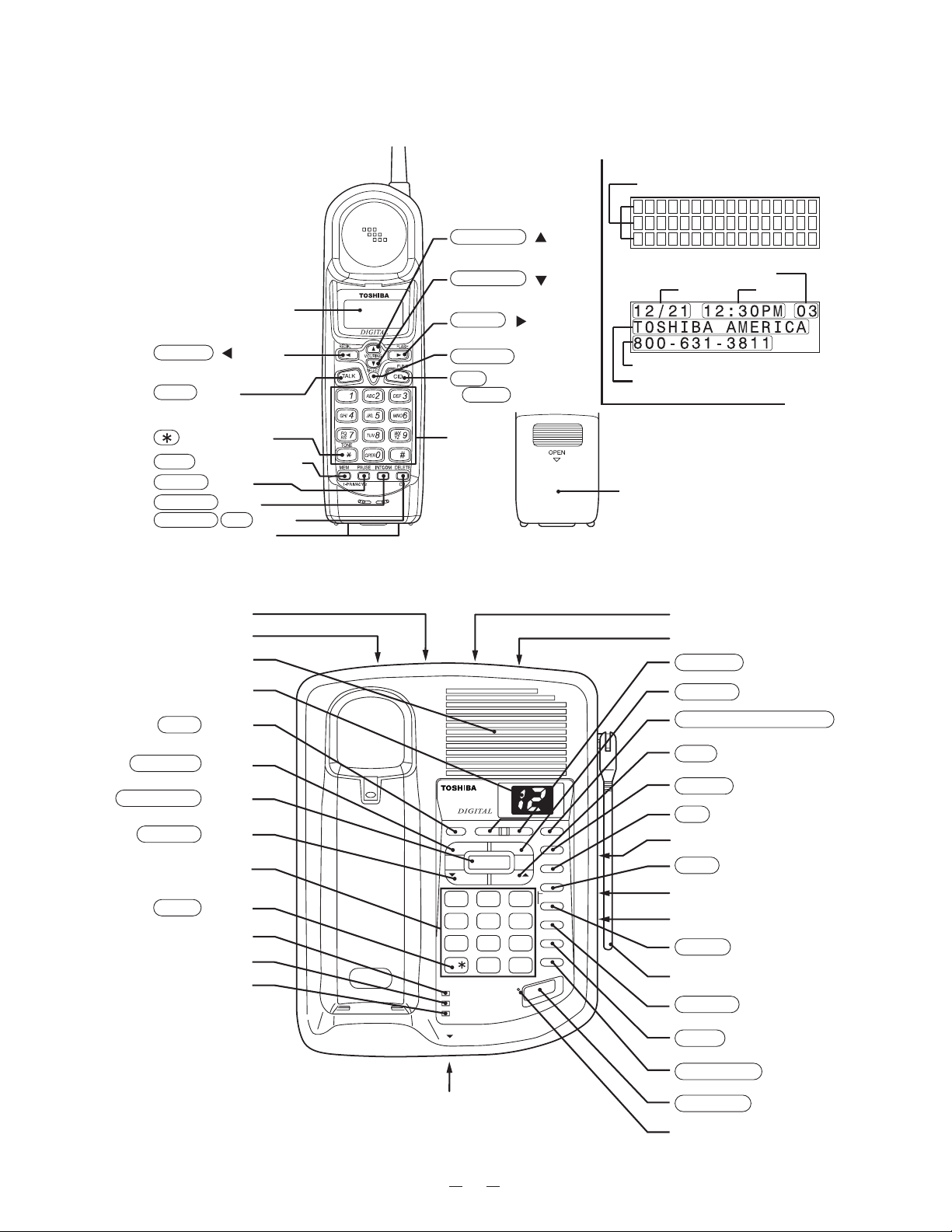
OPERATING CONTROLS
HANDSET CONTROLS AND FUNCTIONS LCD
Dot matrix display
VOL/RING ( ) button
(up arrow button)
VOL/RING ( ) button
Liquid Crystal Display
(LCD)
REDIAL ( ) button
(Left arrow button)
TALK button
(TONE) button
MEM (Memory) button
PAUSE button
INTCOM button
DELETE CH button
Charging contacts
(down arrow button)
FLASH ( ) button
(Right arrow button)
SELECT button
CID (Caller ID)
/ FUNC (Function)
button
dialpad
Caller's telephone number
Caller's name
Battery compartment
Number of calles
Date Time
BASE UNIT CONTROLS AND FUNCTIONS
DC IN 9V jack
TEL LINE jack
Speaker
LED display
OGM button
ANSWER button
900MHz
PLAY/STOP button
REPEAT button
dialpad
TONE button
IN USE LED
CHARGE LED
POWER LED
CALLER ID
FD-9859
OGM
ANSWER DELETE
PLAY/STOP
REPEAT
ABC
1
JKL
GHI
4
PQ
TUV
7
RS
TONE
OPER
IN USE
CHARGE
POWER
MIC
- VOLUME + MEMO REC
SKIP
DEF
3
2
MNO
6
5
WX
9
8
YZ
#
0
SPEAKER
2WAY REC
CLOCK
PIN
MEM
1
PRIVACY
PAUSE
2
INTCOM
HOLD
FLASH/RDL
TONE/PULSE switch
Ringer ON/OFF Switch
VOLUME button
DELETE button
MEMO REC/2WAY REC button
SKIP button
CLOCK button
PIN button
SPEED DIAL INDEX
MEM (Memory) button
REC TIME switch (ANN/4/1)
RING TIME switch (2/4/TS)
PAUSE button
Antenna
INTCOM button
HOLD button
Microphone
2
FLASH/RDL button
SPEAKER button
SPEAKER LED (Green)
Page 4
Base Unit
Transmitter Section
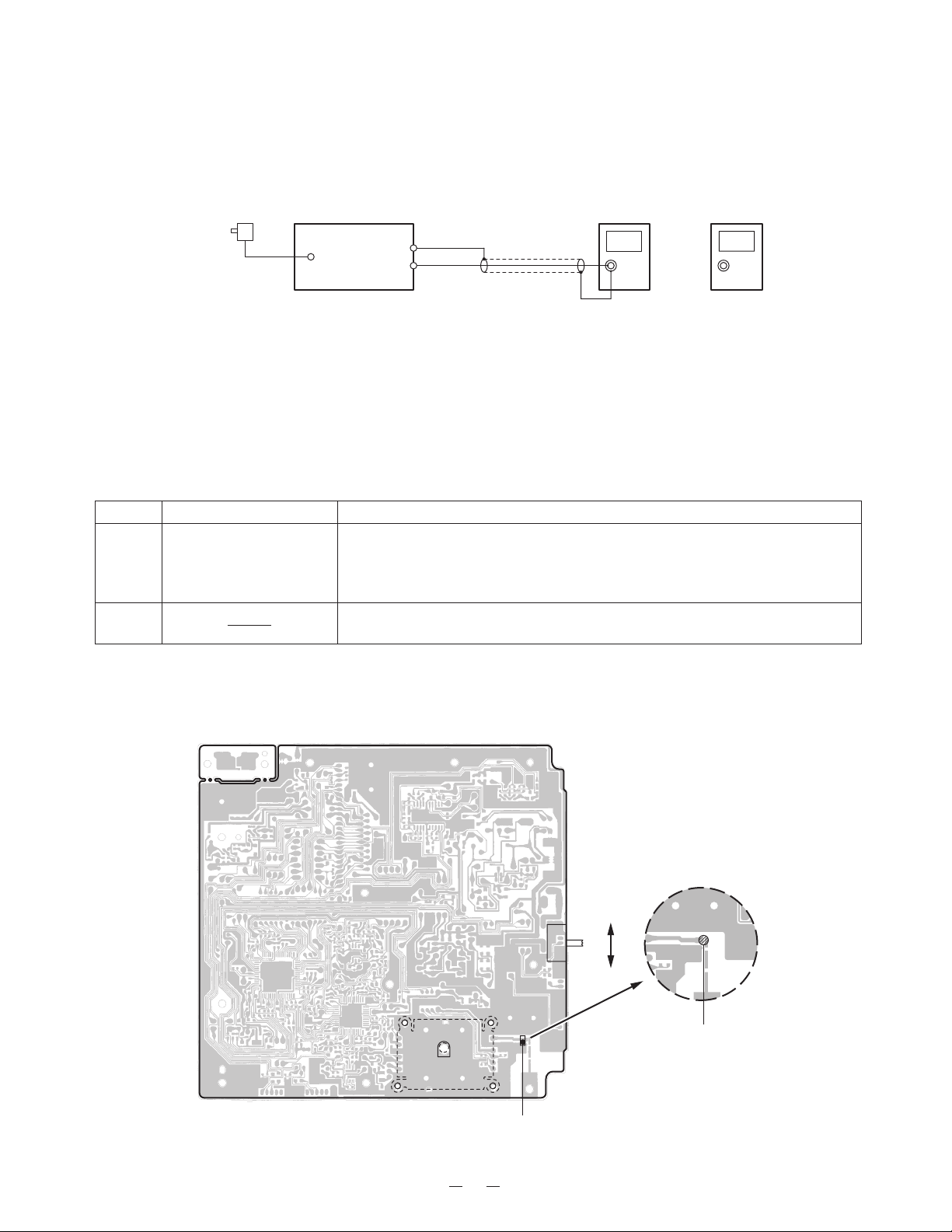
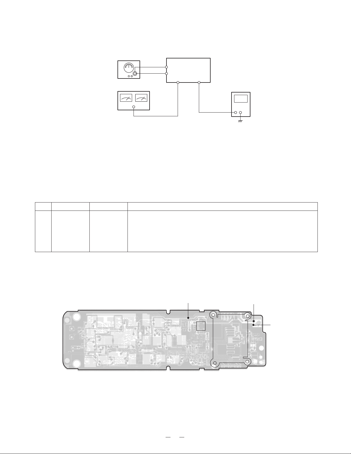
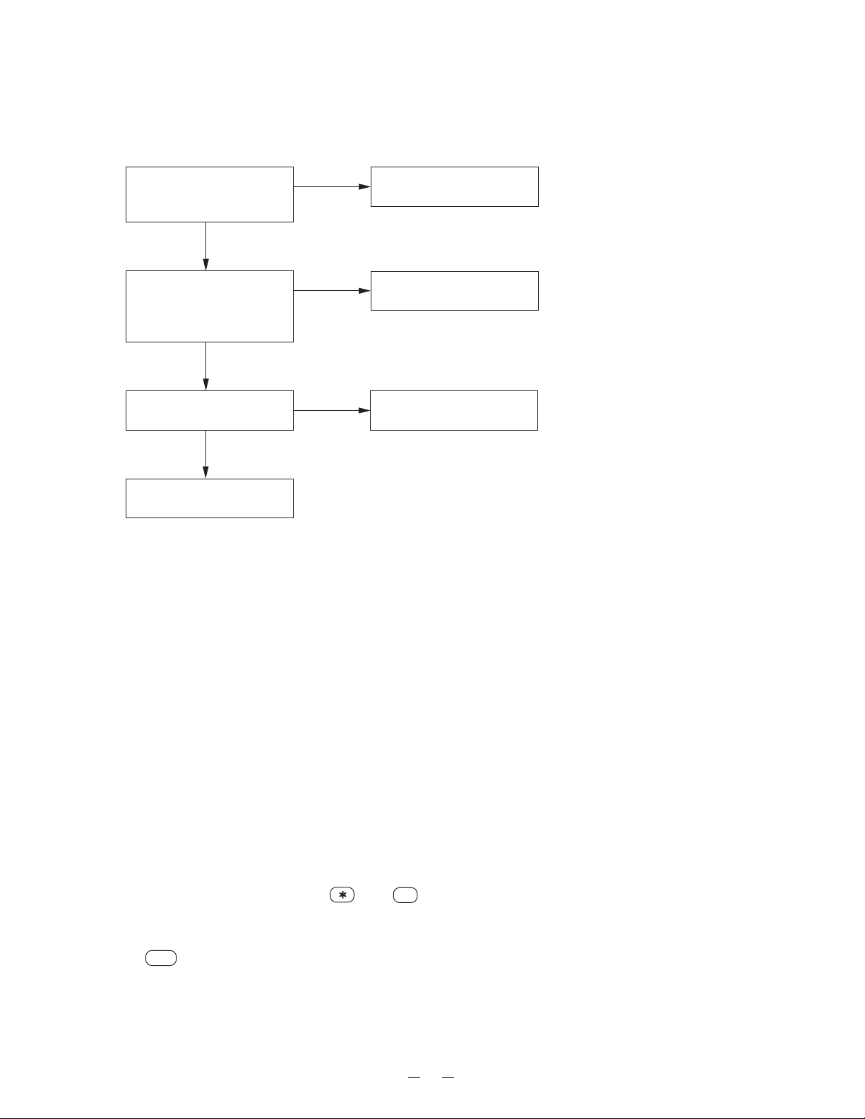
ALIGNMENT PROCEDURE
Connections
AC Adapter
(120V 60Hz)
BASE Unit
Test Point
(J1)
Spectrum Analyzer
FM Deviation Meter
Preset
a) Remove the solder on the pattern (refer to the illust. below).
b) Set the “TONE / PULSE” switch to PULSE.
c) Connect the AC adapter to the base unit while pressing the “INTCOM” key, and keep pressing it continuously.
d) Release the “INTCOM” key after entering TEST mode 1 with CHARGE LED lighting.
Alignment Procedure
step
1
2
Adjustment
VR202
(TX P ower)
Remarks
Connect the Spectrum Analyzer to test point (J1).
Adjust VR202 so that the power instructions of the Spectrum analyzer reaches
-6.0dBm.
Then confirm the frequency is 926.295415 MHz.
Press the “INTCOM” key twice and connect the FM Deviation Meter to test
point J1. Confirm the de viation is 23 ~ 46 kHz.
Alignment Point Location on Base Main PCB and Base RF PCB
Base Main PCB
S1
Base RF PCB
J1
VR202
Test Point
T
P
Remove solder
before alignment
3
Page 5
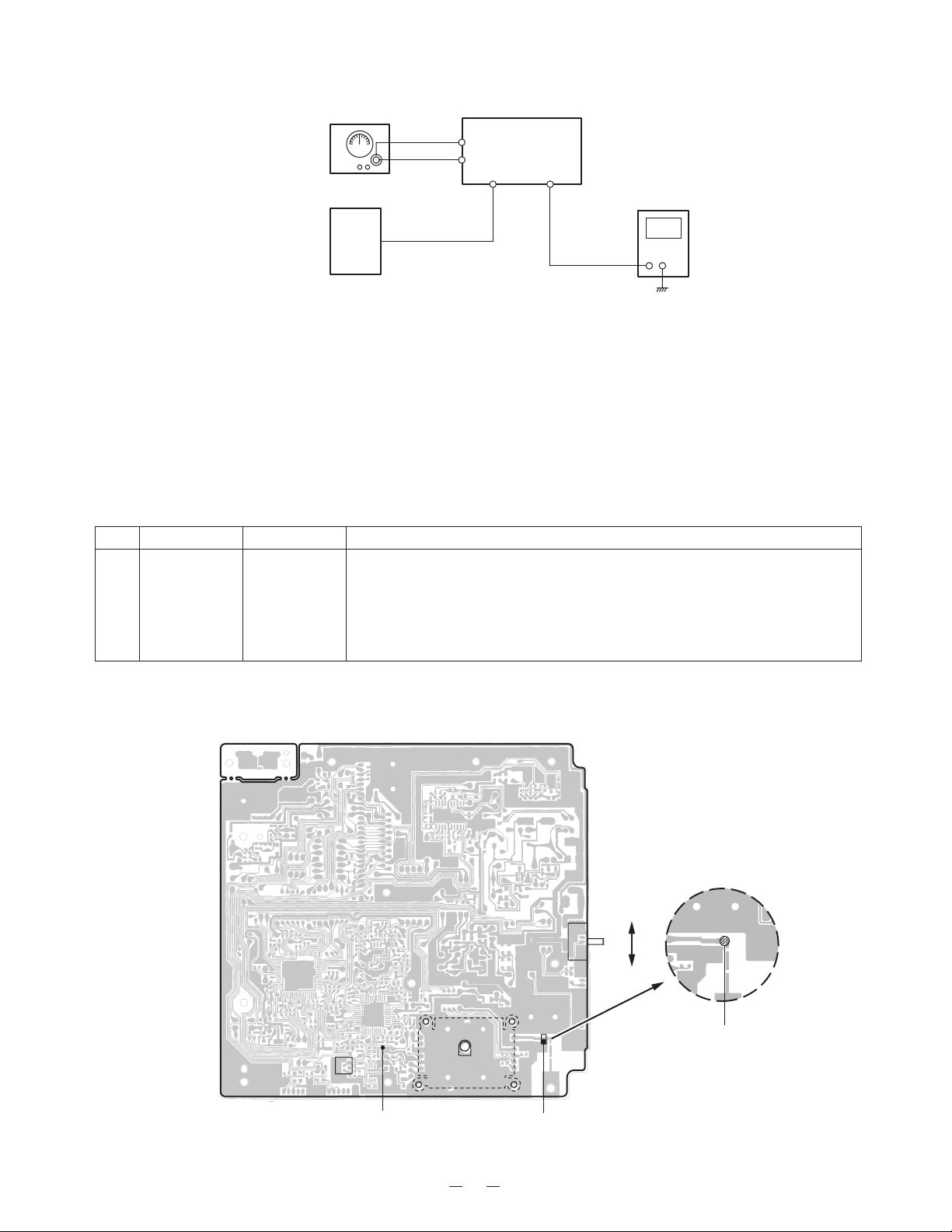
Receiver Section
Connections
AC 120V
60Hz
SG
+
9V Jack
AC
Adapter
Test Point
(J1)
DC IN
BASE Unit
Discriminator
Test Point
DC Voltmeter
Preset
a) Remove the solder on the pattern (refer to the illust. below).
b) Set the “T ONE/PULSE” switch to PULSE.
c) Connect the AC adapter to the base unit while pressing the “INTCOM” key, and keep pressing it continuously.
d) Release the “INTCOM” key after entering TEST mode 1 with CHARGE LED lighting.
Alignment Procedure
step1Preset to
Adjustment
Remarks
Press the “INTCOM” key for 3 times to enter the TEST Mode 4. Connect
SG: 1mV
No modulation
L1
(Discriminator
Voltage)
the RF Signal Generator to the test point (J1) on the Base MAIN PCB.
Make sure that the frequency is 903.417756 MHz.
Connect the DC Voltmeter to the Discriminator test point. Adjust L1 to
indicate DC 0.90 V.
Alignment Point Location on Base Main PCB and Base RF PCB
Base Main PCB
Base RF PCB
J1
L1
VR202
T
S1
P
Remove solder
before alignment
Discriminator Test Point
Test Point
4
Page 6
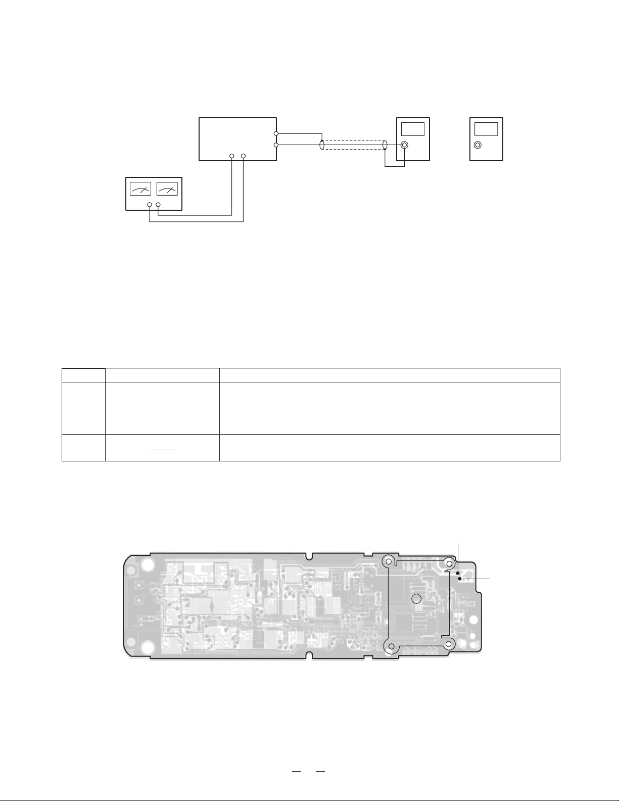
Handset Unit
Transmitter Section
Connection
Handset Unit
Test
Batt
Connector
DC Power Supply
3.8V
Point
(J601)
Preset
a) Remove the solder on the pattern (refer to the illust. below).
b) Connect DC power supply to battery connector on the handset unit.
c) Turn the DC power supply On while pressing “
∗∗
∗ ” and “ # “ keys, and keep pressing the keys continuously.
∗∗
d) Release keys after entering TEST mode 1 with beep.
Alignment Procedure
step
1
2
Adjustment
VR502
Connect the Spectrum Analyzer to test point (J601).
Adjust VR502 so that the power instructions of the Spectrum analyzer reaches
-4.0 dBm.
Then comfirm the frequency is 903.617561 MHz.
Press the “3” key and connect the FM Deviation Meter to test point (J601).
Confirm the deviation is 23 ~ 46 kHz.
Spectrum Analyzer
Remarks
FM Deviation Meter
Alignment Point Location on Handset Main PCB and Handset RF PCB
Handset PCB
RF PCB
VR502
5
Test Point (J601)
Remove solder
Page 7
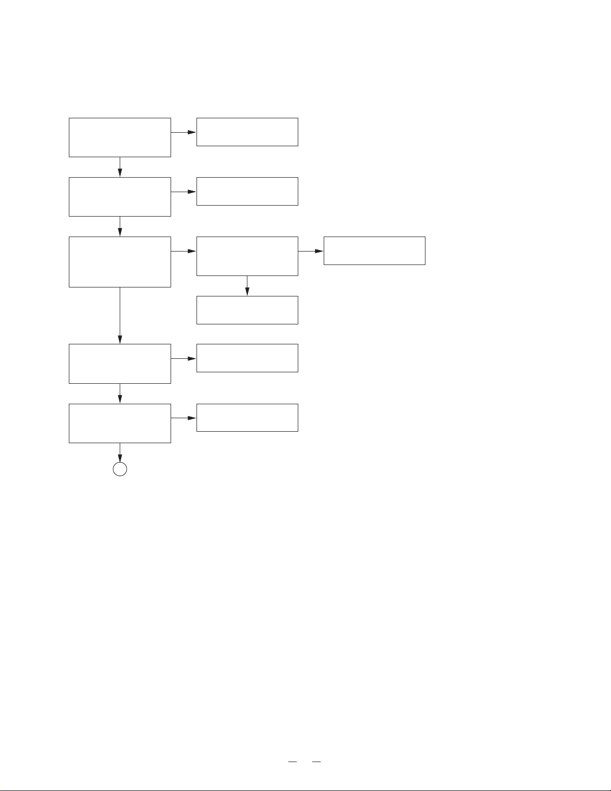
Receiver Section
Connections
RF SG
+
Test Point
(J601)
HANDSET Unit
DC Power Supply
Battery
Connector
DC 3.8V
Discriminator
Test Point
Preset
1) Remove the solder on the pattern (refer to the illust. below).
2) Connect DC power supply to battery connector on the handset unit.
3) Turn the DC power supply ON while pressing “
∗∗
∗ ” and “ # “ keys, and keep pressing the keys continuously.
∗∗
4) Release keys after entering TEST mode 1 with beep.
Alignment Procedure
step1Preset to
SG: 1mV
No modulation
Adjustment
L603
(Discriminator
Voltage)
Press the “4” key to enter the TEST Mode 4. Connect the RF Signal
Generator to the test point (J601) on the handset MAIN PCB. Make sure
that the frequency is 926.495220 MHz.
Connect the DC Voltmeter to the Discriminator test point. Adjust L603 to
indicate DC 0.90 V.
DC Voltmeter
Remarks
Alignment Point Location on Handset Main PCB and Handset RF PCB
Handset PCB
Discriminator Test Point
RF PCB
L603
Test Point (J601)
Remove solder
6
Page 8
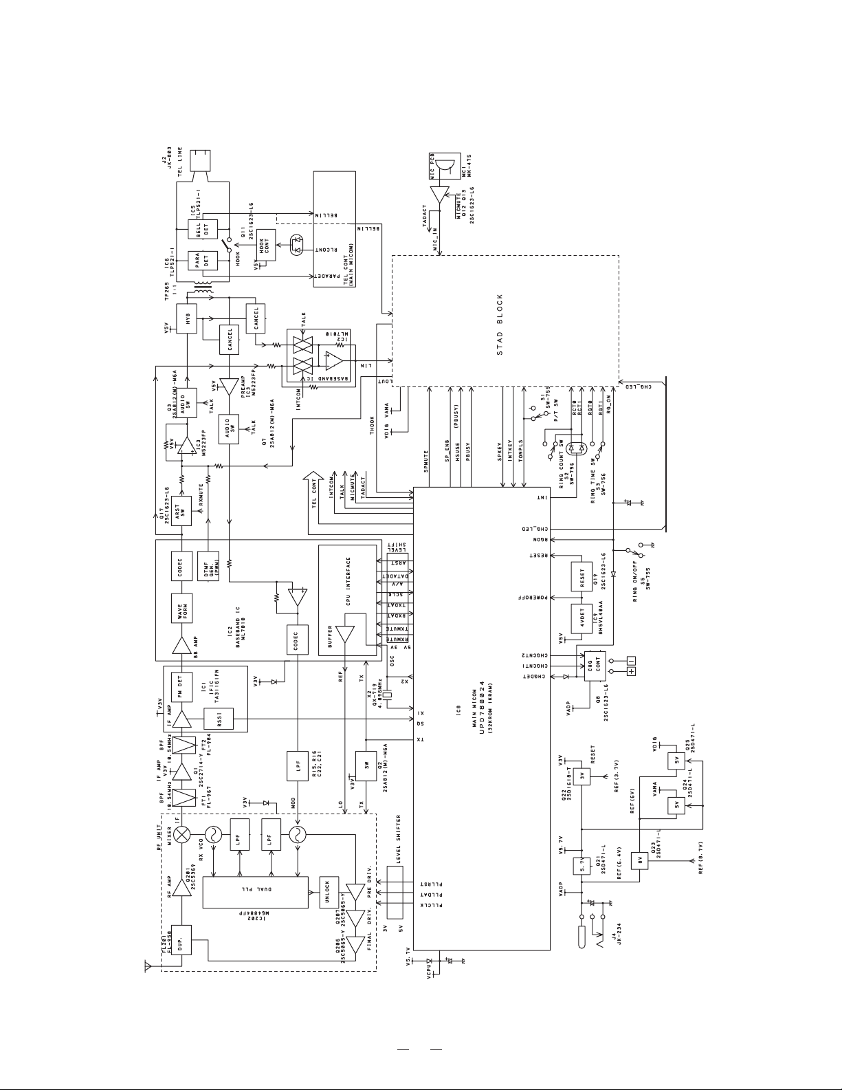
Base Unit, Main
BLOCK DIAGRAMS
7
Page 9
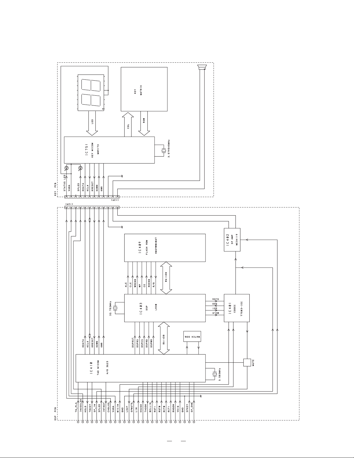
Base Unit, DSP and Key
8
Page 10
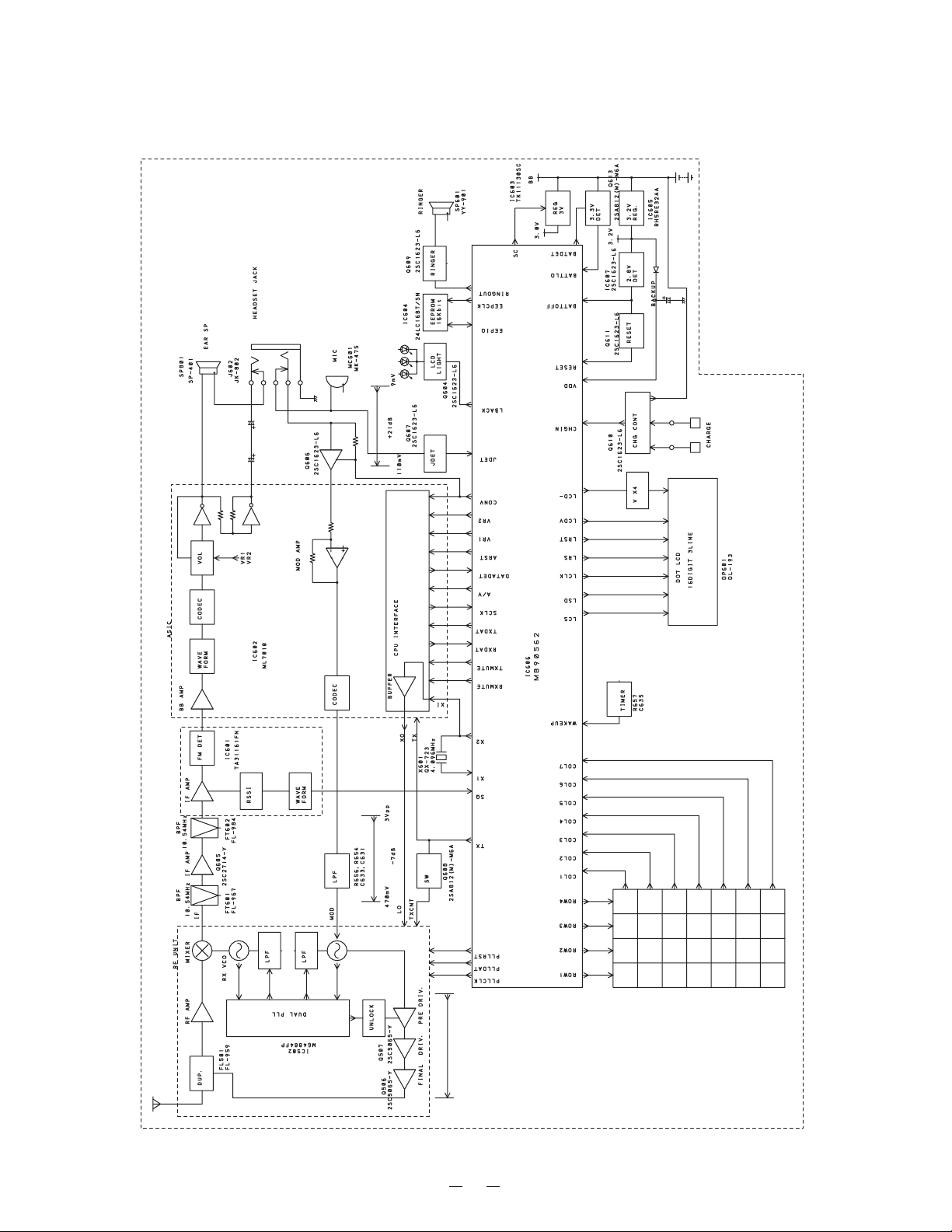
Handset
9
Page 11
Base Unit, Main
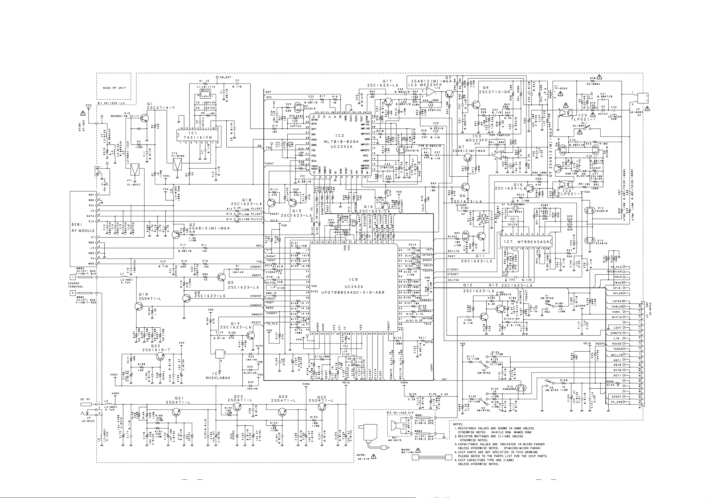
SCHEMATIC DIAGRAMS
10
11
Page 12
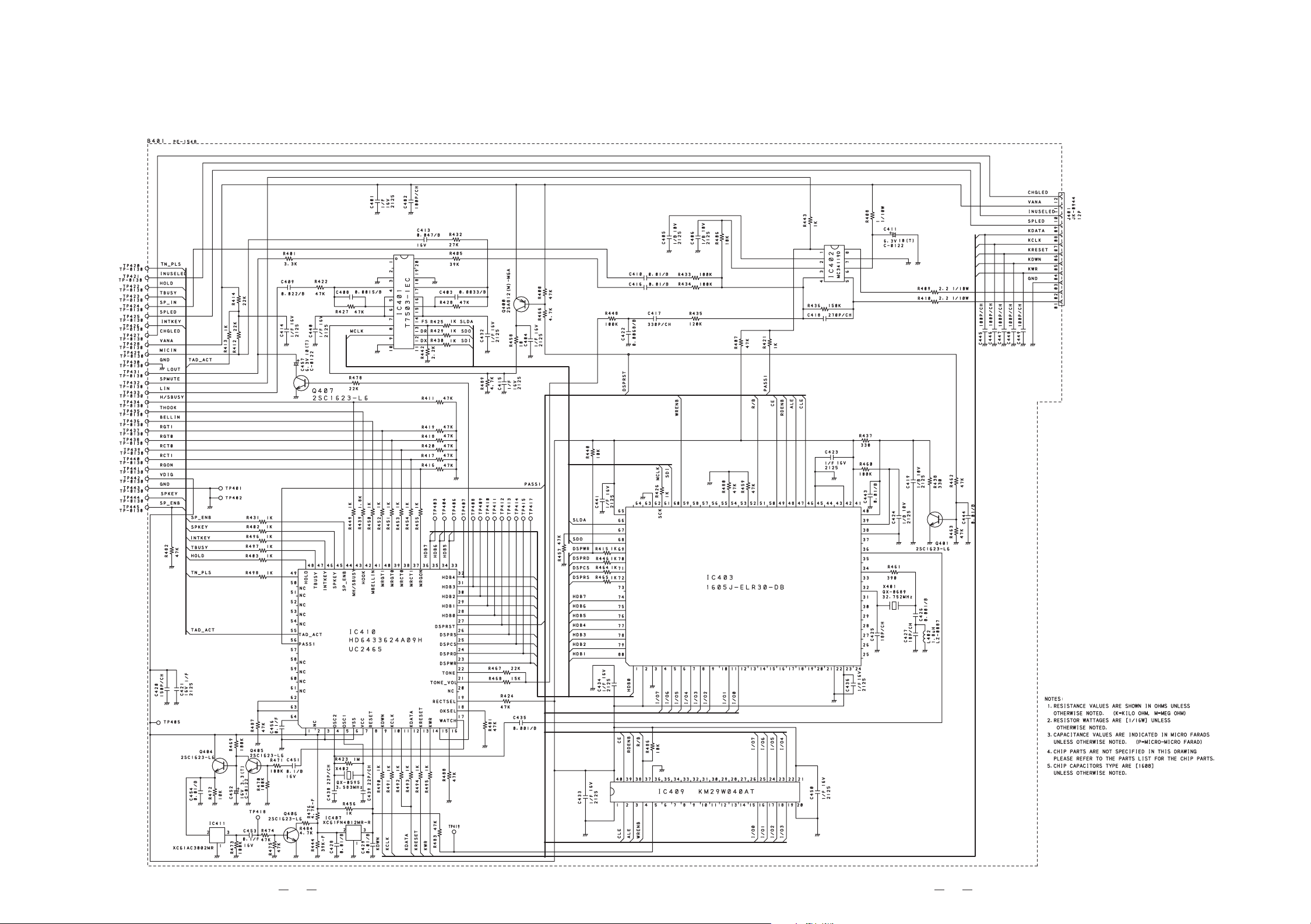
Base Unit, DSP
12
13
Page 13
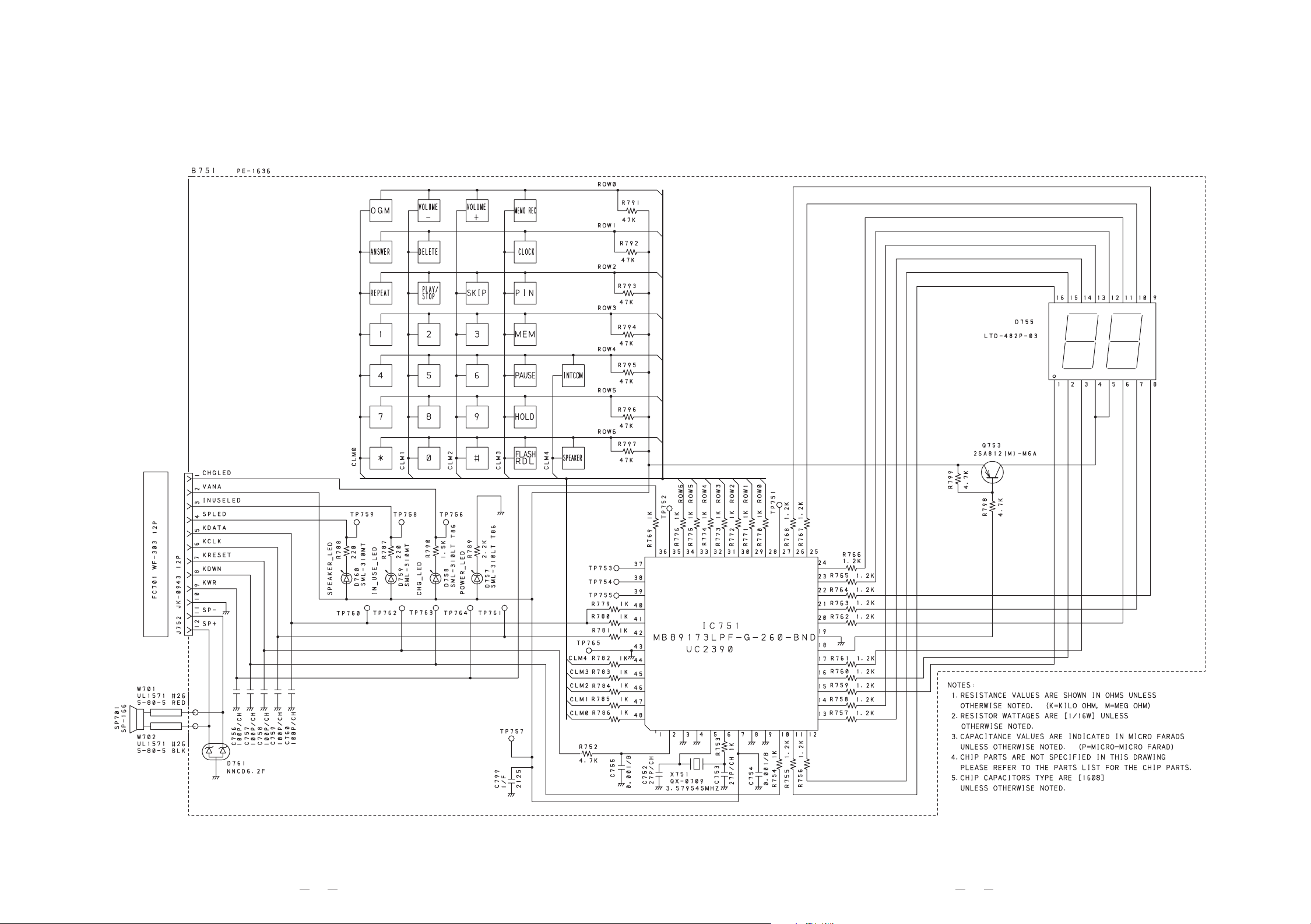
Base Unit, Key
14
15
Page 14
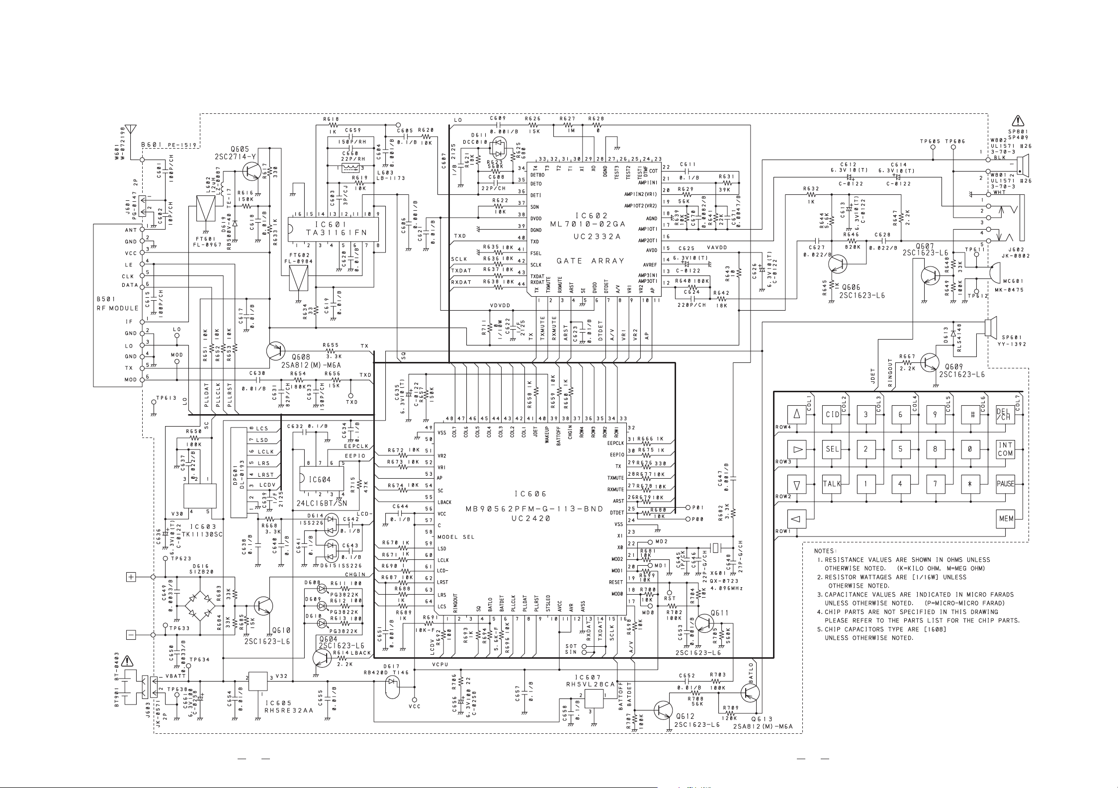
Handset
16
17
Page 15
TROUBLESHOOTING HINTS
1. The bell does not ring.
When the INTCOM of the
base is pressed, does the
ringer on the handset ring?
When the TEL SG is joined
with the base to make bell
signal, is there pulse wave at
pin 4 of IC5?
Is there pulse wave at
pin 49 of IC8?
Check IC8 and its
peripheral circuit.
BASE UNIT
OK
OK
OK
NG
NG
NG
See 2. The bell does not ring
& page does not ring.
Check IC5 and TEL network
circuit.
Check R179.
If you want to reset the unit to the factory settings
You can cancel the OGM, PIN, and the clock settings by the following process.
1) Disconnect the AC adaptor and telephone line cord from the base. Keep the A C adaptor connected to the wall
outlet. Make sure that the telephone line cord remains disconnected during this procedure.
2) While pressing the DELETE button, plug the AC power adaptor into the base. Keep pressing the DELETE
button for more than 4 seconds .
A beep sounds and “ P” blinks in the LED display.
To resume using the unit, connect the telephone line cord and place the handset on the base.
Note:
If you turn on the unit again, “ P” may flash.
HANDSET
Deletion of the Caller ID memory
To delete the Caller ID memory in the EEPROM, proceed with the following process:
1) Connect the battery with pressing and # buttons, and keep pressing the buttons continuously for
approximate 2 seconds.
2) Release buttons when entering TEST mode with beep.
3) Press CID button.
4) A confirmation beep will sound after about 8 seconds, then the data for caller ID is deleted.
(Note: Do not disconnect the battery until you hear the confirmation beep, otherwise the data may not be
completely deleted.)
18
Page 16
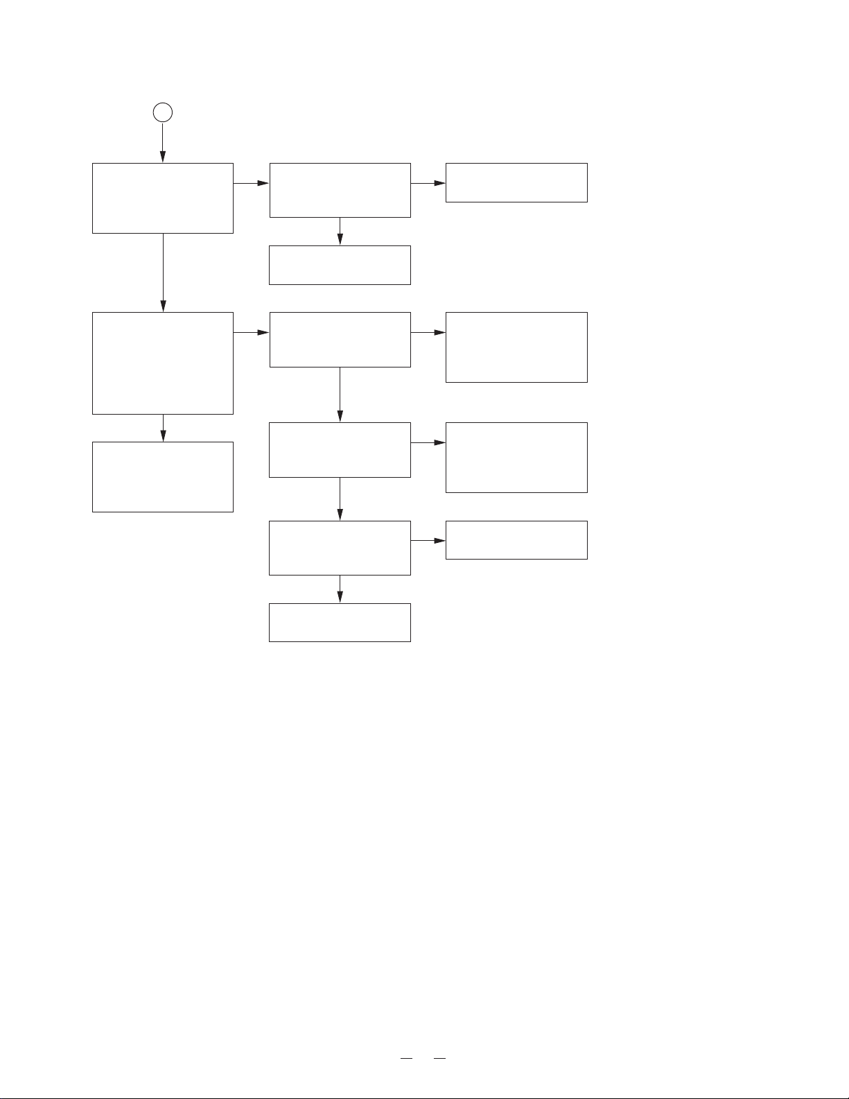
2. The bell does not ring & page does not ring.
Can the base and handset be
connected?
OK
Press handset DIAL key
while in TALK MODE.
Can key touch sound be
heard from the ringer?
OK
When the INTCOM of the
base is pressed, does pin63
of IC8 change from low to
high?
NG
NG
NG
See 3. The base and handset
cannot be connected.
When the key of the handset is
pressed, can the pulse output
at pin 2 of IC606 be seen?
OK
At the Q609 collector, can the
pulse wave be seen?
OK
Check RINGER SP601.
Check R496.
OK
NG
NG
NG
Check IC606.
Check R667 and Q609.
Replace R496.
OK
Check IC8 and its peripheral
circuit.
Check IC410 and key circuit.
19
Page 17
3. The base and handset cannot be connected.
Check whether the base
is able to set in the test
mode 1.
OK
Check the TX POWER
and the TX FREQUENCY
on the base unit.
OK
Press “INTCOM” k ey twice,
check whether deviation of
the TX data is app. ±23
kHz~±46kHz Dev.
OK
Check whether the
handset is able to set in
the test mode 1.
OK
Check the TX POWER
and the TX FREQUENCY
on the handset unit.
OK
NGACheck IC8 and its
peripheral circuit.
NG
Check base RF unit.
Check whether there is a
NG
pulse data waveform at
C19.
OK
Check base RF unit.
NG Check IC606 and its
peripheral circuit.
NG
Check handset RF unit.
Check IC2, Q2 and the
NG
peripheral circuit.
20
Page 18
A
Press “3” key, check
whether deviation of the
TX data is app. ±23kHz
~ ±46kHz Dev.
OK
Press “5” ke y, 926.49522
MHz (30kHz ±30kHz
Dev.) 1mV output signal
from RF jack is applied.
Check whether the bell
ring.
OK
Place the handset on the
base to charge about 10
seconds, then connect
again.
NG Check whether there is a
pulse data waveform at
C630.
OK
Check handset RF unit.
NG Check whether there is
the 30kHz waveform at
C605.
OK
Check whether there is a
30kHz pulse wavef orm at
pin 34 of IC602.
OK
Check whether the
voltage at pin 10 of IC601
is more than 1V.
OK
NG
Check IC602, Q608 and
the periperal circuit.
Check handset RF unit
NG
and the peripheral circuit
of IC601, Q605, FT601,
FT602.
Check R620, R621,
NG
R623, R625, C605, C607,
C608, D611, IC602 and
their peripheral circuit.
Check IC601 and its
NG
peripheral circuit.
Check C606, IC606 and
its peripheral circuit.
21
Page 19
4. Cannot make a phone call (pulse).
Can the base and handset
be connected?
OK
While in TALK MODE, press
dial key of the handset.
Check whether square
waveform from pin 46 of IC8
is fed.
OK
Check R83, D11, Q11, RL1
and the peripheral circuit.
NG
NG
See 3. The base and handset
cannot be connected.
Check IC8 and its peripheral
circuit.
5. Cannot make a phone call (tone).
Can the base and handset be
connected?
OK
NG
See 3. The base and handset
be cannot be connected.
While in TALK MODE, press
dial key of the handset.
Can tone waveform from Pin
23 of IC2 is fed?
OK
Can tone signal be heard
from the handset speaker?
OK
Check the base TEL-line
circuit and RELAY control
circuit.
NG
NG
Check IC2 and its peripheral
circuit.
Check IC3, Q3, Q4 and the
peripheral circuit.
22
Page 20
6. Voice cannot be transmitted to other party (outgoing call).
Can the base and handset be
connected?
OK
The 1 kHz, 3.3mV sine
waveform is applied to
+
MC601
sine waveform from collector
of Q606 be fed?
Check whether there is the
1 kHz sine waveform at pin
12 of IC602.
Check whether there is the
1 kHz sine waveform at pin
22 of IC2.
Check whether there is the
1 kHz sine waveform at the
Q4 collector.
side, can the 1 kHz
OK
OK
OK
OK
NG
NG
NG
NG
NG
See 3. The base and handset
cannot be connected.
Check Q606 and its
peripheral circuit.
Check IC602 and the
peripheral circuit.
Check IC2 and the peripheral
circuit.
Check IC2, Q4 and the
pripheral circuit.
Check whether the 1 kHz sine
waveform from TEL-line
output is fed.
OK
Check MC601 of handset.
NG
Check T1, RL1 and their
pripheral circuits.
23
Page 21
7. The voice of the caller cannot be heard (incoming call).
Can the base and handset be
connected?
OK
The 1 kHz, 75.0mV sine
waveform is applied to TELline of the base, can the 1 kHz
sine waveform from the Q7
collector be fed?
OK
Check whether there is the
1 kHz sine waveform at
pin 12 of IC2.
OK
Check whether there is the
1 kHz sine waveform at pin
17 ot IC602.
OK
Check whether there is the
1 kHz sine wavef orm between
1 and 2 of SP801.
OK
NG
NG
NG
NG
NG
See 3. The base and handset
cannot be connected.
Check the base TEL-line
circuit and REPLAY control
circuit.
Check IC2 and its peripheral
circuit.
Check C611, R631, R629,
R639, R641, C670, C671.
Check C612, C614, W801,
W802.
Check SP801.
24
Page 22

8. The voice of the caller cannot be recorded.
Check hearing the OGM
when push OGM key.
OK
When 1 kHz -20dBm sine
waveform is applied to TELline of the base, can the sine
wave be seen at TP433?
OK
Can the sine wave be seen
at pin 6 of IC401?
OK
Check around IC401, IC403,
and IC409.
NG
NG
NG
Check around IC401, IC403,
IC409, IC410 and IC751.
Can the sine wave be seen
at pin 17 of IC2?
OK
Check around IC401.
Check around IC402.
NG
Check TEL network primary
circuit.
9. Outgoing message cannot be transmitted to other party.
Can the voice wave be seen
at pin 1 of IC401 when OGM
key is pressed?
OK
Can the voice wave be seen
at TP431?
OK
Check TEL network primary
circuit.
NG
NG
Check around IC401, IC403,
IC409, IC410 and IC751.
Check around IC401.
25
Page 23

IC AND TRANSISTOR VOLTAGE CHART
Base Unit Unit[V] Unit[V]
Ref. No. PIN STBY TALK NOTE Ref. No. PIN STBY TALK NOTE
1 2.8 2.8
2 2.8 2.8
3 2.8 2.8
4 1.4 1.4
5 0.0 0.0
6 2.8 2.8
7 2.8 2.8
IC1 8 2.8 2.8
9 2.8 2.8
10 0.4 2.2
11 1.9 1.9 Sine wave
12 2.0 1.9 Sine wave
13 2.8 2.8
14 0.9 1.0 Random
15 0.0 0.0
16 1.0 1.0
1 2.8 0.0
2 0.0 2.8
3 0.0 2.8
4 2.8 2.8
5 0.0 0.0
6 3.0 3.0
7 0.0 3.0
8 0.0 2.8
9 0.0 0.0
10 0.0 2.8
11 3.0 2.9
12 1.4 1.4
13 1.4 1.4
IC2 14 1.4 1.4
15 3.0 2.9
16 1.4 1.4
17 1.4 1.4
18 0.0 0.0
19 1.2 1.4
20 1.4 1.4
21 1.4 1.4
22 1.4 1.4
23 0.0 0.0
24 0.0 0.0
25 0.0 0.0
26 0.0 0.0
27 0.0 0.0
28 1.3 1.3 Sine wave
IC2 36 1.5 1.5 Random
IC3
IC5
IC6
IC7 6 2.4 2.4 Sine w a ve
29 1.2 1.2 Sine wave
30 3.0 3.0
31 3.0 3.0
32 3.0 3.0
33 3.0 3.0
34 1.5 1.5 Pulse
35 1.5 1.5 Random
37 0.0 0.0
38 3.0 3.0
39 0.0 0.0
40 0.0 1.4 Pulse
41 0.0 0.0
42 2.6 2.6 Pulse
43 0.3 0.5 Pulse
44 0.0 0.6 Pulse
1 2.6 2.5
2 2.6 2.5
3 2.6 2.5
4 0.0 0.0
5 2.6 2.5
6 2.5 2.5
7 2.5 2.5
8 5.1 5.1
1 1.1 1.1
2 1.1 1.1
3 0.0 0.0
4 5.1 5.1
1 0.3 0.3
2 1.0 1.0
3 0.0 0.0
4 0.5 0.5
1 2.5 2.5
2 2.6 2.5
3 2.6 2.5
4 2.6 2.5
5 0.0 0.0
7 2.7 2.7 Sine w a v e
8 0.0 0.0
9 5.1 5.1
10 5.1 5.1
11 5.1 5.1
12 0.0 0.0
26
Page 24

Unit[V] Unit[V]
Ref. No. PIN STBY TALK NOTE Ref. No. PIN STBY TALK NOTE
13 0.0 0.0
14 5.1 5.1
15 5.1 5.1
IC7
IC8 18 0.0 1.0 Random
16 5.1 5.1
17 0.0 0.0
18 2.6 2.6
19 2.6 2.6
20 2.5 2.5
1 0.8 0.8
2 0.0 5.0
3 0.0 0.0
4 0.0 0.0
5 5.1 0.0
6 0.0 5.1
7 5.1 5.1
8 0.0 5.1
9 0.0 0.0
10 5.1 5.1
11 3.9 3.9
12 5.2 5.2
13 3.7 3.7
14 5.1 0.0
15 0.0 5.1
16 5.1 0.0
17 0.0 5.1
19 0.4 1.0 Random
20 4.6 4.5 Pulse
21 5.1 5.1
22 0.2 0.2
23 0.0 0.0
24 5.1 5.1
25 0.0 0.0
26 5.1 5.1
27 0.0 0.0
28 5.3 5.3
29 5.2 5.2
30 5.2 5.2
31 5.1 5.1
32 0.0 0.0
33 0.4 2.2
34 3.0 3.0
35 5.1 5.1
36 5.1 5.0
IC8 50 0.0 5.0
IC9 2 5.8 5.8
IC401 7 0~2.4 0~2.4
37 0.0 0.0
38 5.1 5.1
39 0.0 0.0
40 3.1 3.1 Sine wav e
41 2.7 2.7 Sine wav e
42 0.0 0.0
43 5.0 5.0 Random
44 5.0 5.0 Random
45 0.0 0.0 Random
46 0.0 5.0
47 0.0 0.0
48 3.7 3.7
49 5.1 5.1
51 0.0 0.0
52 5.0 4.9
53 5.1 5.0
54 5.1 5.0
55 0.0 0.0
56 5.2 5.1
57 5.2 5.1
58 5.1 5.1
59 0.2 0.2
60 0.0 0.0
61 0.0 0.0
62 0.0 0.0
63 0.0 0.0
64 0.0 0.0
1 5.2 5.2
3 0.0 0.0
1 1.5~2.3 1.5~2.3
2 1.5~2.3 1.5~2.3
30
4 0~2.4 0~2.4
5 0~2.4 0~2.4
6 0.1 0.1
8 5.2 5.2
9 2.6 2.6
10 0 0
11 0.1 0.1
12 0.1 0.1
13 0 0
27
Page 25

Unit[V] Unit[V]
Ref. No. PIN STBY TALK NOTE Ref. No. PIN STBY TALK NOTE
14 1 1
15 0 0
16 2.4 2.4
IC401 17 0 0
18 0 0
19 0 0
20 0 0
1 3.7 3.7
2 2.2 2.2
3 2.2 2.2
IC402
IC403 15 0.0 0.0
4 2.2 2.2
5 2.2 2.2
6 5.3 5.3
7 0.0 0.0
8 2.2 2.2
1 0.0 0.0
2 5.3 5.3
3 0.0 0.0
4 0.0 0.0
5 0.0 0.0
6 0.0 0.0
7 0.0 0.0
8 0.0 0.0
9 0.0 0.0
10 0.0 0.0
11 0.0 0.0
12 0.0 0.0
13 0.0 0.0
14 0.0 0.0
16 0.0 0.0
17 0.0 0.0
18 0.0 0.0
19 0.0 0.0
20 0.0 0.0
21 0.0 0.0
22 0.0 0.0
23 5.3 5.3
24 0.0 0.0
25 0.0 0.0
26 0.0 0.0
27 0.0 0.0
28 0.0 0.0
29 0.0 0.0
IC403 51 5.3 5.3
30 0.0 0.0
31 0.0 0.0
32 0.0 0.0
33 0.0 0.0
34 0.0 0.0
35 0.0 0.0
36 1.2 1.2
37 2.9 2.9
38 0.0 0.0
39 5.2 5.2
40 5.0 5.0
41 5.3 5.3
42 0.0 0.0
43 0.0 0.0
44 0.0 0.0
45 0.0 0.0
46 0.0 0.0
47 0.0 0.0
48 5.3 5.3
49 5.3 5.3
50 0.0 0.0
52 0.0 0.0
53 0.0 0.0
54 5.3 5.3
55 0.0 0.0
56 5.3 5.3
57 5.3 5.3
58 5.3 5.3
59 5.3 5.3
60 0.0 0.0
61 2.6 2.6
62 0.0 0.0
63 0.0 0.0
64 0.0 0.0
65 5.3 5.3
66 0.0 0.0
67 0.0 0.0
68 0.0 0.0
69 5.3 5.3
70 5.2 5.2
71 5.2 5.2
72 5.2 5.2
73 0.0 0.0
28
Page 26

Unit[V] Unit[V]
Ref. No. PIN STBY TALK NOTE Ref. No. PIN STBY TALK NO TE
74 0.0 0.0
75 0.0 0.0
76 0.0 0.0
IC403 77 0.0 0.0
78 0.0 0.0
79 0.0 0.0
80 0.0 0.0
1 0.0 0.0
IC407 2 4.7 4.7
3 5.3 5.3
1 0.0 0.0
2 0.0 0.0
3 0.0 0.0
4 0.0 0.0
5 5.2 5.2
6 0.0 0.0
7 0.0 0.0
8 0.0 0.0
9 0.0 0.0
10 0.0 0.0
11 0.0 0.0
12 0.0 0.0
13 0.0 0.0
14 0.0 0.0
15 0.0 0.0
16 0.0 0.0
IC409 17 0.0 0.0
18 0.0 0.0
19 0.0 0.0
20 0.0 0.0
21 5.3 5.3
22 0.0 0.0
23 0.0 0.0
24 0.0 0.0
25 0.0 0.0
26 0.0 0.0
27 0.0 0.0
28 0.0 0.0
29 0.0 0.0
30 0.0 0.0
31 0.0 0.0
32 0.0 0.0
33 0.0 0.0
34 0.0 0.0
IC409
IC410 19 5.3 5.3
35 0.0 0.0
36 0.0 0.0
37 5.3 5.3
38 5.3 5.3
39 5.3 5.3
40 5.3 5.3
1 5.0 5.0
2 0.0 0.0
3 0.0 0.0
4 2.7 2.7
5 2.4 2.4
6 0.0 0.0
7 5.3 5.3
8 5.3 5.3
9 5.3 5.3
10 5.3 5.3
11 0.0 0.0
12 0.0 0.0
13 5.3 5.3
14 5.3 5.3
15 5.3 5.3
16 0.0 0.0
17 2.7 2.7
18 0.0 0.0
20 0.0 0.0
21 0.0 0.0
22 0.0 0.0
23 5.3 5.3
24 5.3 5.3
25 5.3 5.3
26 5.3 5.3
27 0.0 0.0
28 0.0 0.0
29 0.0 0.0
30 0.0 0.0
31 0.0 0.0
32 0.0 0.0
33 0.0 0.0
34 0.0 0.0
35 0.0 0.0
36 0.0 0.0
37 5.0 5.0
38 0.0 0.0
29
Page 27

Unit[V] Unit[V]
Ref. No. PIN STBY TALK NOTE Ref. No. PIN STBY TALK NOTE
39 0.0 0.0
40 0.0 0.0
41 5.1 5.1
42 5.1 5.1
43 0.0 0.0
44 0.0 0.0
45 0.0 0.0
46 0.0 0.0
47 0.0 0.0
48 0.0 0.0
49 5.0 5.0
50 0.0 0.0
IC410 51 0.0 0.0
52 0.0 0.0
53 0.0 0.0
54 0.0 0.0
55 0.0 0.0
56 3.6 3.6
57 0.0 0.0
58 0.0 0.0
59 0.0 0.0
60 0.0 0.0
61 0.0 0.0
62 0.0 0.0
63 0.0 0.0
64 3.6 3.6
1 0.0 0.0
IC411 2 0.0 0.0
3 0.0 0.0
1 0 0 OPEN
25 5
3 0 0 GND
4 0 0 GND
5 1.5(AC) 1.5(AC)
6 4.5(AC) 4.5(AC)
7 5.2 5.2
IC751 8 0 0 GND
9 0 0 GND
10 5.2 5.2
11 5.2 5.2
12 5.2 5.2
13 5.2 5.2
14 5.2 5.2
15 5.2 5.2
IC751 32 5 5
Q1 E 0.0 0.0
Q2 E 3.0 3.0
Q3 E 2.6 2.5
16 5.2 5.2
17 5.2 5.2
18 5.2 5.2
19 0 0 GND
20 5.2 5.2
21 5.2 5.2
22 5.2 5.2
23 5.2 5.2
24 5.2 5.2
25 5.2 5.2
26 5.2 5.2
27 0 0 OPEN
28 5 5
29 5 5
30 5 5
31 5 5
33 5 5
34 5 5
35 0 0 OPEN
36 5 5
37 0 0 OPEN
38 0 0 OPEN
39 0 0 OPEN
40 0 0
41 0 0
42 5.2 5.2
43 0 0 GND
44 0 0
45 0 0
46 0 0
47 0 0
48 0 0
B 0.7 0.7
C 1.7 1.7
B 4.8 2.3
C 0.0 2.9
B 5.1 1.9
C 2.6 2.5
30
Page 28

Unit[V] Unit[V]
Ref. No. PIN STBY TALK NOTE Ref. No . PIN STBY T ALK NO TE
B 1.2 1.2
Q4 E 0.5 0.5
C 4.1 4.1
B 0.0 0.0
Q5 E 0.0 0.0
C 4.9 4.9
B 0.0 0.6
Q6 E 0.0 0.0
C 5.1 0.0
B 5.1 1.9
Q7 E 2.6 2.5
C 2.6 2.5
B 0.7 0.7
Q8 E 0.0 0.0
C 0.0 0.0
B 0.8 0.8
Q9 E 1.0 1.0
C 0.3 0.3
B 0.7 1.1 Random
Q10 E 0.0 0.6 Random
C 0.0 1.0 Random
B 0.0 0.7
Q11 E 0.0 0.0
C 11.2 0.0
B 0.3 0.0
Q12 E 0.9 0.0
C 1.6 0.0
B 1.3 0.0
Q13 E 0.7 0.0
C 4.1 0.0
B 0.6 3.0 Random
Q14 E 0.0 3.0 Random
C 0.0 5.1 Random
B 2.7 2.7 Pulse
Q15 E 2.7 2.6 Pulse
C 4.5 4.5 Pulse
B 0.6 0.6
Q16 E 0.0 0.0
C 0.0 0.0
B 0.0 2.1
Q17 E 1.4 1.4
C 1.4 1.4
Q18 E 0.0 0.0
Q19 E 0.0 0.0
Q21 E 6.0 6.0
Q22 E 3.0 3.0
Q23 E 8.3 8.3
Q24 E 5.2 5.2
Q25 E 5.2 5.2
Q400 E 5.3 5.3
Q401 E 0.0 0.0
Q404 E 0.0 0.0
Q405 E 0.0 0.0
Q406 E 0.0 0.0
Q407 E 0.0 0.0
Q753 E 5.2 5.2
B 0.7 0.7
C 0.0 0.0
B 0.0 0.0
C 5.1 5.0
B 6.5 6.6
C 11.2 10.6
B 3.7 3.7
C 5.8 5.8
B 8.9 8.9
C 11.2 10.6
B 5.8 5.8
C 8.3 8.3
B 5.8 5.8
C 7.9 7.3
B 4.6 4.6
C 5.3 5.3
B 0.0 0.0
C 5.2 5.2
B 0.0 0.0
C 5.3 5.3
B -0.5 -0.5
C 0.0 0.0
B 0.0 0.0
C 4.7 4.7
B 0.6 0.6
C 0.0 0.0
B 4.4 4.4
C 5.2 5.2
31
Page 29

Handset Unit[V] Unit[V]
Ref. No. PIN STBY TALK NOTE Ref. No. PIN STBY TALK NOTE
1 OPEN OPEN
2 OPEN OPEN
3 0.0-2.8 2.8 Pulse
4 OPEN OPEN
5 GND GND
6 0.0-2.8 2.8 Pulse
7 0.0-2.8 2.8 Pulse
IC601 8 0.0-2.8 2.8 Pulse
9 0.0-2.8 2.8 Pulse
10 0.0-0.4 2.2 Pulse
11 OPEN OPEN
12 0.0-2.0 2.2-2.6 Float Float
13 0.0-2.8 0.0-2.0 Float Float
14 0.4-1.0 0.4-1.2 Float Float
15 GND GND
16 OPEN OPEN
1 0.0-2.8 0.2 Pulse
2 0.0 2.8
3 0.0 2.8
4 0.0-2.8 2.8 Pulse
5 GND GND
6 0.0-3.0 3.0 Pulse
7 0.0 3.0
8 0.0 2.8
9 0.0 0.0 Vol Low Vol Low
10 0.0-2.8 2.8
11 0.0 2.8
12 0.0-0.8 1.4 Pulse
13 0.0-0.8 1.4
IC602 14 0.0-0.8 1.4
15 0.0-3.0 3.0 Pulse
16 0.0-0.6 1.4 Pulse
17 0.0-0.6 1.4 Pulse
18 GND GND
19 0.0-0.6 1.4 Pulse
20 0.0-0.6 1.4 Pulse
21 0.0 0.0
22 0.0-0.6 1.4 Pulse
23 OPEN OPEN
24 OPEN OPEN
25 OPEN OPEN
26 OPEN OPEN
27 GND GND
28 0.0-3.0 0.0-3.2 Pulse Pulse
Pulse, V ol Low
Vol Low
IC602 36 0.2-1.8 1.4-1.8 Float Float
IC603 3 0.0-1.2 1.2
IC604
IC605 2 3.8 3.8
IC607 2 3.2 3.2
IC606 5 0.0 0.0-2.6 Pulse
29 0.8-2.8 Pulse Pulse
30 OPEN OPEN
31 OPEN OPEN
32 OPEN OPEN
33 OPEN OPEN
34 OPEN OPEN
35 0.6-2.6 0.6-2.6 Float Float
37 0.0-3.0 3.0 Pulse Pulse
38 0.0-3.0 3.0 Pulse
39 GND GND
40 0.0 0.0-3.0 Pulse
41 0.0 0.0
42 0.0-3.0 0.0-3.0 Pulse Pulse
43 0.0-3.0 0.0-3.0 Pulse Pulse
44 0.0-3.0 0.0-3.0 Pulse Pulse
1 0.0-2.8 0.0-2.8 Pulse Pulse
2 GND GND
4 0.0-3.0 3.0 Pulse
5 3.8 3.8
1 OPEN OPEN
2 OPEN OPEN
3 OPEN OPEN
4 GND GND
5 2.8 2.8
6 0.0-2.8 2.8 Pulse
7 GND GND
8 3.2 3.2
1 GND GND
3 3.2 3.2
1 3.2 3.2
3 GND GND
1 0.0-0.2 2.8 Pulse
2 0.0 0.0
3 OPEN OPEN
4 0.0-0.8 2.1 Pulse
6 0.0 0.0-3.0 Pulse
7 0.0 0.0
8 0.0 0.0
9 0.0-2.8 2.8 Pulse
32
Page 30

Unit[V] Unit[V]
Ref. No. PIN STBY TALK NOTE Ref. No. PIN STBY TALK NOTE
10 OPEN OPEN
11 2.8-3.0 2.8 Pulse
12 2.8-3.0 2.8 Pulse
13 GND GND
14 0.0 0.0
15 0.0-2.8 0.0-2.8 Pulse Pulse/Tone
16 0.0-3.0 0.0-3.0 Pulse Pulse
17 0.0 2.8
18 2.8-3.0 2.8 Pulse
19 2.8-3.0 2.8 Pulse
20 2.8-3.0 2.8 Pulse
21 0.0 0.0
22 0.4-3.0 0.4-3.0 Sine wave Sine wave
23 0.0-3.0 0.0-3.0 Sine wave Sine wave
24 GND GND
25 0.0 3.0
26 0.0-2.8 2.8 Pulse
27 0.0 2.8
28 0.0 2.8
29 0.0-2.8 2.8 Pulse
30 2.8-3.2 2.8 Pulse
31 0.0-2.8 2.8 Pulse
IC606 32 OPEN OPEN
33 2.8-3.0 2.8 Pulse
34 2.8-3.0 2.8
35 2.8-3.0 2.8
36 2.8-3.0 2.8
37 2.8-3.0 2.8 Pulse
38 3.2 3.2 Charge Off
39 1.0-2.9 2.9 Pulse
40 0.0-2.9 2.9
41 0.0 0.0
42 0.0 0.0
43 0.0 0.0
44 0.0 0.0
45 0.0 0.0
46 0.0 0.0
47 0.0 0.0
48 OPEN OPEN
49 GND GND
50 0.0 0.0
51 0.0-2.8 2.8
Pulse, H/S Jack Off H/S Jack Off
Pulse, V ol Low Vol Low
IC606 59 0.0 0.0-2.8 Pulse
Q604 E GND GND
Q605 E GND GND
Q606 E 0.0-0.2 0.2 Pulse
Q607 E GND GND
Q608 E 0.0-3.0 3.0
Q609 E GND GND
Q610 E GND GND
Q611 E GND GND Pulse
Q612 E GND GND
Q613 E 3.8 3.8
54 0.0-2.8 2.8 Pulse
55 0.0 2.8
56 2.8-3.0 3.0 Pulse
57 2.8-3.0 3.0 Pulse
58 OPEN OPEN
60 0.0-2.8 2.8 Pulse
61 0.0 0.0-2.8 Pulse
62 0.0 0.0-2.8 Pulse
63 0.0 0.0-2.8 Pulse
64 0.0-2.8 0.0-2.8 Pulse
B 0.0 0.0
C 2.4 2.4
BackLightOff BackLightOff
BackLightOff BackLightOff
B 0.0-0.7 0.7 Pulse
C 0.0-1.6 1.2-1.8 Pulse Float
B 0.0-0.7 0.7 Pulse
C 0.0-1.2 1.2 Pulse
B 0.0-0.7 0.7 Pulse
C 0.0-2.8 0.0 Pulse
B 0.0-2.8 2.3
C 0.1 2.8
B 0.0 0.0
C 0.0 2.8
B 0.0 0.0
C 2.8-3.0 2.8 Pulse
B 0.0 0.0
C 2.8-3.0 2.8 Pulse
B 0.0 0.0
C 3.7 3.7
B 3.8 3.8
C 0.0 0.0
52 0.0 0.0 Vol Low Vol Lo w
53 0.0 3.0
33
Page 31

Base Unit
SEMICONDUCTOR LEAD IDENTIFICATION
D1/D23/D24 : 1N4148
D3 : HZ7C3
D9 : HZ33CP
D20 : HZ4A1
D21 : HZ7A1
D22 : HZ9B2
Anode
Cathode
D5/D7/D8/D14/D25 : RLS4148
Cathode
Anode
Q1 : 2SC2714
Q2/Q3/Q7/Q9/Q400/Q753 : 2SA812(M)
Q4 : 2SC2712
Q5/Q6/Q8/Q10/Q11/Q12/Q13
/Q14/Q15/Q16/Q17/Q19/Q401
/Q404/Q405/Q406/Q407 : 2SC1623
B
E
B : Base
E : Emitter
C : Collector
C
IC1
TA31161FN
OSC IN
OSC OUT
MIX OUT
GND 1
DEC
MIX IN
Vcc
1
2
3
BS
4
5
6
7
8
INPUT
15
GND
14
DET OUT
13
Vcc
12
LIMIT OUT
11
LIMIT OUT
10
RSSI
9
Vcc
16
IC3 :BA10358F
OUTPUT1 1
NEGATIVE1 2
POSITIVE1 3
GND 4
IC5/IC6
-
1
+
2
+
-
8 V+
7 OUTPUT2
6 NEGATIVE2
5 POSITIVE2
IC9 : RH5VL40AA
TLP521
1
23
4
D2/D10 : DCC010
Anode/Cathode
D15 : RB500V
Cathode
Q18/Q21/Q23
/Q24/Q25 : 2SD471
E
C
IC2
ML7010-02GA
TX
TXMUTE
RXMUTE
ARST
SE
VDD
DATADET
AV
VR1
VR2
2
1
D4/D11/D12 : DCB010
D6/D13 : DCA010
D16 : HSM88WA
Cathode
Cathode Anode
AnodeAnode
D757/D758 : SML-310LT
D759/D760 : SML-310MT
Anode
Cathode
Anode
Anode
Cathode Cathode
D761 : NNCD6.2F
Anode
Cathode Cathode
Q22 : 2SD1618
D755 :LTD-482P
Cathode G1
Cathode A1
Cathode F1
Cathode B1
Cathode B2
Cathode F2
Cathode A2
B
1
2
3
4
5
6
7
8
9
10
11AP
RXDATA44
TXDATA43
SCLK42
12AMP3OT1
13AMP3IN1
14AVREF
FSEL41
TXD40
15AVcc
16AMP20T1
DGND39
VDD38
SDN37
17AMP1OT1
18AGND
19AMP1OT2
DET136
DETO35
20AMPIN1
21AMPIN1
DETBO34
22COT
ECB
B: Base
C: Collector
E: Emitter
MONI_433
MONI_332
MONI_231
MONI_130
XI29
XO28
DGND27
TEST326
TEST225
TEST124
DTMF23
IC7
16 15 14 13 12 11 10 9
DIGIT 1 DIGIT 2
F1
E1
12345678
Cathode C1
A1
G1
D1
Cathode E1
Cathode D1
B1
F2
C1
E2
Anode 1
A2
G2
D2
Anode 2
Cathode D2
Cathode G2
B2
C2
Cathode E2
Cathode C2
MT88E45ASR
1
VREF
2
IN1+
3
IN1-
4
GS1
5
Vss
6
OSC1
7
OSC2
8
CB0
9
3
DCLK
DATA
10
20
19
18
17
16
15
14
13
12
11
IN2+
IN2GS2
CB2
CB1
DD
V
CD
ST/GT
EST
DR/STD
34
Page 32

IC8
µPD780024AGC
P50/A8
P51/A9
P52/A10
P53/A11
P54/A12
P55/A13
P56/A14
P57/A15
SS0
V
DD0
V
P30
P31
P32
P33
P34/SI31
P35/SO31
IC410
HD6433624
1
2
3
4
5
6
7
8
9
10
11
12
P47/AD764
P46/AD663
17P36/SCK31
18P20/SI30
6
7
/AN
/AN
6
7
PB
CVcc
PB
P45/AD562
P44/AD461
P43/AD360
P42/AD259
P41/AD158
P40/AD057
P67/ASTB56
P66/WAIT55
19P21/SO30
20P22/SCK30
21P23RxD0
VTref
TONED
25AVSS26P17/ANI7
22P24/TxD0
23P25/ASCK0
24V
DD1
P87P86P85P84P83P82P81P80P77P76P7
P65/WR54
P64/RD53
27P16/ANI6
28P15/ANI5
P75/BUZ5229P14/ANI4
P74/PCL5130P13/ANI3
5
P73/TI51/TO515031P12/ANI2
P72/TI50/TO504932P11/ANI1
42
3514
3415
IC403
1605CJ
80 HDB1
79 HDB2
78 HDB3
77 HDB4
76 HDB5
75 HDB6
74 HDB7
73 NC
72 RS
71 CD
70 RD
69 WR
68 SDO
67 SLDB
66 SLDA
65 VDD
HD87 1
V
DD
2
V
SS
P71/TI0148
P70/TI00/TO047
P03/INTP3/ADTRG46
P02/INTP245
P01/INTP144
P00/INTP043
SS1
V
X141
X240
IC39
XT138
XT237
RESET3613
DD
AV
REF
AV
P10/ANI03316
3
FDB7 4
FDB6 5
FDB5 6
FDB4 7
FDB3 8
FDB2 9
NC 10
FDB1 11
FDB0 12
NC 13
NC 14
VAB13 15
VAB12 16
NC 17
VAB11 18
VAB10 19
VAB9 20
VAB8 21
V
SS
22
V
DD
23
VAB7 24
VAB6 25
VAB5 26
VAB4 27
VAB3 28
VAB2 29
34
32
1IN
NC 33
1OUT
VAB1 30
VAB0 31
XTAL
XTAL
36
2IN
NC 35
XTAL
64 NC
63 NC
62 VSS
61 SCKA
60 SDI
59 WE
58 NC
57 NC
56 VROM Chip Enable
55 VAB14
54 VAB15 / CS / CONF2
53 NC
52 VAB16 / CONF0
51 R / B / DO
50 NC
49 Flash Chip Select / CONF1
48 Read Enable / SK / CONF3
47 Address Latch Enable / DI
46 Command Latch Enable
45 VSS
44 CKO
43 NC
42 VSS
41 VDD
37
38
SS
V
2OUT
RSTB 39
VDDPU 40
XTAL
P2
0
/IRQ4/ADTRG
IC401
T7503-1EC
VFROP0
VF
R
ON0
GNDA0
VFxIN0
VFxIP0
GSx0
VCM0
VDD
MCLK
GNDD
OSC
OSC
TEST
RES
P2
1
/SCK
P22/SI
P23/SO
P24/SCK
P25/RXD
P2
6
/TXD
P2
7
/IRQ
X11
2
X
Vss
2
1
Vcc
1
1
1
3
0
1
2
3
4
5
6
7
8
9
10
646362616059585756555453525150
2
3
4
5
6
7
8
9
10
11
12
13
14
15
16
181920212223242526272829303132
2
1P14
/IRQ
/IRQ
/TMIF 17
6
5
3
P1
P1
/IRQ
7
P1
20
VFROP1
19
VF
R
ON1
18
GNDA1
17
VFxIN1
16
VFxIP1
15
GSx1
14
VCM1
13
FS
12
D
R
11
Dx
/TMIG
3
P1
/TMOFH
2
P1
3PA2PA1
PA
/TMOW
/TMOFL
0
1
P1
P1
IC402
MC34119D
CD
FC2
FC1
Vin
49
48
4
P7
47
P7
3
46
P7
2
45
P7
1
44
P7
0
43
P6
7
42
P6
6
41
P6
5
40
P6
4
39
P6
3
38
P6
2
37
P6
1
36
P6
0
35
P56/WKP
34
33
0
1
2
3
4
/WKP
/WKP
/WKP
/WKP
/WKP
0
1
2
3
4
P5
P5
P5
P5
P5
8
1
2
3
4
VO2
7
Gnd
6
Vcc
5
VO1
7
P56/WKP
6
P55/WKP
5
IC409
KM29W040AT
1
Vss
2
CLE
3
ALE
4
WE
5
WP
6
N.C.
7
N.C.
8
N.C.
9
N.C.
10
N.C.
11
N.C.
12
N.C.
13
N.C.
14
N.C.
15
N.C.
16
I/O0
17
I/O1
18
I/O2
19
I/O3
20
Vss
IC751
MB89173LPF
40
Vcc
39
CE
38
RE
37
R / B
36
GND
35
N.C.
34
N.C.
33
N.C.
32
N.C.
31
N.C.
30
N.C.
29
N.C.
28
N.C.
27
N.C.
26
N.C.
25
I/O7
24
I/O6
23
I/O5
22
I/O4
21
Vcc
P4048
P4147
P4246
1DTMF
2RST
3MDD0
4MDD1
5X0
6X1
7Vcc
8P50 / (X0A)
9P51(Z1A)
10P27
11P26
12P25
13P24
14P23
15P22
IC407
XC61FN4012MR
IC411
XC61AC3002MR
P4345
16P21
P4444
17P20
Vss43
18P17
P30 / SDK42
19Vss
P31 / S041
20P16
Vout
P32 / S140
21P15
P33 / EC39
22P14
P34 / TO / INT038
23P13
Vin
P35 / INT137
24P12
Vss
P36 / INT236
P37 / BZ35
P00 / L1034
P01 / L1133
P02 / L1232
P03 / L1331
P04 / L1430
P05 / L1529
P06 / L1628
P07 / L1727
P1026
P1125
35
Page 33

Handset
D608/D609/D610 : PG3822K
Cathode
Anode
D617 : RB420D
Cathode
(open)Anode
IC601
TA31161FN
Vcc
1
2
3
BS
4
5
6
7
8
OSC IN
OSC OUT
MIX OUT
GND 1
DEC
MIX IN
D611 : DCC010
D614/D615 : 1SS226
D619 : RB500V
Cathode
16
INPUT
15
GND
14
DET OUT
13
Vcc
12
LIMIT OUT
11
LIMIT OUT
10
RSSI
9
Vcc
Cathode / Anode
Cathode Anode
IC602
ML7010-02GA
TXMUTE
RXMUTE
DATADET
Anode
ARST
VDD
VR1
VR2
Anode
D616 : S1ZB20
-
+
~~
D613 : RLS4148
Cathode
Q604/Q606/Q607/Q609
/Q610/Q611/Q612 : 2SC1623
Q605 : 2SC2714
Q608/Q613 : 2SA812(M)
B
E
SCLK42
FSEL41
14AVREF
15AVcc
C
TXD40
DGND39
VDD38
16AMP20T1
17AMP1OT1
18AGND
SDN37
DET136
DETO35
19AMP1OT2
20AMPIN1
21AMPIN1
DETBO34
MONI_433
MONI_332
MONI_231
MONI_130
XI29
XO28
DGND27
TEST326
TEST225
TEST124
DTMF23
22COT
B : Base
E : Emitter
C : Collector
RXDATA44
TXDATA43
TX
SE
AV
1
2
3
4
5
6
7
8
9
10
11AP
12AMP3OT1
13AMP3IN1
IC606
MB90562PFM
64 P44/PPG3
1P45/PPG4
2P46/PPG5
3P50/AN0
4P51/AN1
5P52/AN2
6P53/AN3
7P54/AN4
8P55/AN5
9P56/AN6
10P57/AN7
11AVcc
12AVR
17P63/INT7/DTT1
63 P43/PPG2
62 P42/PPG1
61 P41/PPG0
18MD0
19RST
20MOD1
60 P40/SCK0
59 P37/SOT0
58 P36/SIN0
21MOD2
22X0
23X1
57 C
24Vss
P35/RTO5
Vcc55P34/RTO454
56
25P00
26P01
27P02
P33/RTO353
28P03
P32/RTO25229P04
P31/RTO15130P05
P30/RTO05031P06
Vss4932P07
36
P27/IN348
P26/IN247
P25/IN146
P24/IN045
P23/TO144
P22/TIN143
P21/TO042
P20/TIN041
P17/FRCK40
P16/INT639
P15/INT538
P14/INT437
P13/INT33613AVss
P12/INT23514P60/SIN1
P11/INT13415P61/SOT1
P10/INT03316P62/SCK1
IC603
TK11130SCL
Vin5
1on/off Control
2GND
IC604
24LC16BT/SN
Vout4
3Np(Vref)
IC605 : RH5RE32AA
IC607 : RH5VL28CA
1A0
2A1
4Vss
Vcc8
WP7
6
SCLA2 3
SDA5
3
2
1
Page 34

Base Unit
Main PCB
ELECTRICAL PARTS LOCATION
37
Page 35

Base Unit
DSP PCB
38
Page 36

Base Unit
Key PCB
39
Page 37

Handset
Main PCB
40
Page 38

Base Unit
WIRING DIAGRAMS
41
42
Page 39

Handset
43
Page 40

EXPLODED VIEWS AND MECHANICAL PARTS LIST
Base Unit
16
2
31
19
10
32
17
4
12
SPEAKER
22
27
28
5
24
22
MAIN PCB
22
18 26
1
13
23
11
6
14
9
22
KEY PCB
22
25
33
15
3
7
24
8
20
30
7
RF MODULE (BASE)
24
21
ANTENNA
29
44
Page 41

Base Unit
LOC.
NO. NO.
PART NO.
1 RC009181 GNBZ443207Z BUTTON, FUNCTION ABS 1
2 RC005608 RCUN451804Z CUSHION NEOPRENE 2
3 RC009045 GCAS243201Z CASE, BOTTOM ABS 1
4 RC009180 GCAS243206Z CASE, TOP ABS 1
5 RC008414 HTML442750Z CHARGE TERMINAL C5191(PBP) 2
6 RC009182 GNBZ443208Z BUTTON, FUNCTION ABS 1
7 RC002384 LFUT428079Z FOOT BUMPON SJ-5916 1.6T 4
8 RC005689 LHDZ453179Z HOLDER, MIC CR 1
9 RC005444 HHDS431080B HOLDER, SPEAKER
10 RC009046 GCAS445155Z HOOK ABS 1
11 RC008013 RBLD459155A HIMELON 1
12 RC005439 GCAS254442Z DISPLA Y WINDOW PMMA 1
13 RC008942 LNBZ358537Z KEY RUBBER SI 1
14 RC008891 GHDZ350921Z HOLDER, DISPLA Y ABS 1
15 RC009184 PLBZ443486Z LABEL, T A POLYESTER 1
16 RC005329 PLBZ456718Z LABEL, INDICATION 1
17 RC009185 PLBZ443488Z LABEL, INDICATION 1
18 RC008818 GCAS458189Z LED LENS PMMA 1
19 RC008939 GCAS458534Z LED LENS PMMA 1
20 RC009183 PLBB443487Z LABEL, BARCODE PAPER 1
21 RC005688 KDPZ457908Z PLATE, DISPLAY PC 1
22 RC000941 SSCW802608N SCREW, P TIGHT BIND HD + D2.6×8 NI 25
23 RC008289 SSCW192005N SCREW, BIND HD + M2×5 NI 4
24 RC004028 SSCW802616N SCREW, P TIGHT BIND HD + D2.6×16 NI 6
25 RC001752 SSCW283012N SCREW, TAPPING BIND+& SP WASHER D3×12 NI 1
26 RC008611 RETC435649Z SPACER 4
27 RC005436 HSDC356624Z SHIELD COVER SPTE 1
28 RC004794 GSDC353527Z SHIELD CASE ABS.NI PLATING. 1
29 RC008262 GCAS443211Z ST AND ABS 1
30 RC003239 HTML430029Z TOUCHER, RF C5191R-H,T=0.3 1
31 RC005696 RUTC457032Z WOOL COATED PAPER, W OOL TACK 2
32 RC008156 RBLD459208Z HIMELON 1
33 RC009173 LETC441127Z HIMELON T APE 4
REF.
DESCRIPTION QTY
SUS304 CSP 0.8T 3/4H OR H
1
45
Page 42

Handset
7
16
17
5
MAIN PCB ASSY
18
17
8
1
15
22
4
RF MODULE
(HANDSET)
17
11
21
10
13
20
19
6
12
14
2
9
3
23
46
Page 43

Handset
LOC.
NO. NO.
PART NO.
1 RC008346 RBLD442400Z BLIND PC 1
2 RC009055 GNBZ443171Z BUTTON, FUNCTION ABS 1
3 RC009188 GCAS343167Z CASE, FRONT ABS 1
4 RC009051 GCAS343168A CASE, REAR ABS 1
5 RC008342 HTML442336Z CHARGE TERMINAL C2680(BSP) 2
6 RC008703 GCAS457897Z COVER ELASTOMER 1
7 RC009053 GCAS443169Z COVER, BATTERY ABS 1
8 RC008347 RCUM441150Z CUSHION, BATTERY MOLTPRENE, 40×20×8 1
9 RC008348 RCUN442433Z CUSHION, SPEAKER NEOPRENE 1
10 RC008709 LHDZ456969Z HOLDER, MIC EPDM 1
11 RC009054 GHDZ443170A HOLDER, SPEAKER ABS 1
12 RC008464 LNBZ342420Z KEY RUBBER SI 1
13 RC009189 PLBS443491Z LABEL, ID 1
14 RC009057 KDPZ443173Z PLATE, DISPLAY PC 1
15 RC008289 SSCW192005N SCREW, BIND HD + M2×5 NI 2
16 RC003327 SSCW802610N SCREW, P TIGHT BIND HD + D2.6×10 NI 2
17 RC000941 SSCW802608N SCREW, P TIGHT BIND HD + D2.6×8 NI 8
18 RC008465 RCUN443255Z CUSHION, RF MODULE NBR 1
19 RC008466 RCUN459780Z CUSHION, DISPLAY NEOPRENE 1
20 RC008456 GHDZ459779Z HOLDER, DISPLAY PC 1
21 RC008457 RETC459777Z REFLECTION SHEET 1
22 RC000940 SSCW802006N SCREW, P TIGHT BIND HD + D2×6 NI 2
23 RC009021 LPAK442703Z CAP CR 1
REF.
DESCRIPTION QTY
47
Page 44

PARTS LIST
PRODUCT SAFETY NOTE : Products marked with a have special characteristics important to safety.
Before replacing any of these components, read carefully the product safety notice of this service manual.
Don’t degrade the safety of the product through important servicing.
Symbol F G J K M N Z P
% ± 1 ± 2 ± 5 ± 10 ± 20 ± 30 -20+80 0+100
LOC.
NO. NO.
CAPACITORS
The following codes indicate v ariation of capacitors against temper atures,:
YA=±5%, YB=±10%, YD=+20-30%, YE=+20-50%(-25~+85°C), ZF=+30-80%,(-10~+79°C),
CH=0±60ppm/°C, TH=-470ppm/°C , ±60ppm/°C , B=±10%, F=+30-80%,
SL=+350ppm/°C~-1000ppm/°C, UJ=-750ppm/°C ±120ppm/°C , CJ=0±120ppm/°C , CK=0±250ppm/°C
C1 RC005204 BCML811025Z CERAMIC M/L (1608) 0.001UF 50V K B
C2 RC005202 BCML311045Z CERAMIC M/L (1608) 0.1UF 16V K B
C4 RC005224 BCMT813091Z CERAMIC M/L (1608) 3PF 50V C CJ
C5 RC008645 BCMN811514Z CERAMIC M/L (1608) 150PF 50V J RH
C6 RC008646 BCMN812204Z CERAMIC M/L (1608) 22PF 50V J RH
C7 RC005202 BCML311045Z CERAMIC M/L (1608) 0.1UF 16V K B
C8 RC005205 BCML811035Z CERAMIC M/L (1608) 0.01UF 50V K B
C11 RC005205 BCML811035Z CERAMIC M/L (1608) 0.01UF 50V K B
C12 RC005202 BCML311045Z CERAMIC M/L (1608) 0.1UF 16V K B
C13 RC005210 BCMM811014Z CERAMIC M/L (1608) 100PF 50V J CH
C14 RC005210 BCMM811014Z CERAMIC M/L (1608) 100PF 50V J CH
C15 RC005210 BCMM811014Z CERAMIC M/L (1608) 100PF 50V J CH
C16 RC005210 BCMM811014Z CERAMIC M/L (1608) 100PF 50V J CH
C17 RC005204 BCML811025Z CERAMIC M/L (1608) 0.001UF 50V K B
C18 RC005210 BCMM811014Z CERAMIC M/L (1608) 100PF 50V J CH
C19 RC005202 BCML311045Z CERAMIC M/L (1608) 0.1UF 16V K B
C20 RC008926 BCMM518214Z CERAMIC M/L (1608) 820PF 25V J CH
C21 RC005219 BCMM814704Z CERAMIC M/L (1608) 47PF 50V J CH
C22 RC005420 BCMM811514Z CERAMIC M/L (1608) 150PF 50V J CH
C23 RC005204 BCML811025Z CERAMIC M/L (1608) 0.001UF 50V K B
C24 RC005401 BCXT111055Z CERAMIC M/L (2125) 1UF 10V K B
C25 RC008731 BCXK311050Z CERAMIC M/L (2125) 1UF 16V Z F
C26 RC005359 BCMM812204Z CERAMIC M/L (1608) 22PF 50V J CH
C27 RC005207 BCML813325Z CERAMIC M/L (1608) 0.0033UF 50V K B
C28 RC008757 BCMM818204Z CERAMIC M/L (1608) 82PF 50V J CH
C29 RC005275 BCML813925Z CERAMIC M/L (1608) 0.0039UF 50V K B
C31 RC005204 BCML811025Z CERAMIC M/L (1608) 0.001UF 50V K B
C32 RC008008 BCMM812714Z CERAMIC M/L (1608) 270PF 50V J CH
C34 RC001802 BCAZ314706Z ELECTROLYTIC 47UF 16V M C-156
C35 RC005202 BCML311045Z CERAMIC M/L (1608) 0.1UF 16V K B
C36 RC001802 BCAZ314706Z ELECTROLYTIC 47UF 16V M C-156
C37 RC005202 BCML311045Z CERAMIC M/L (1608) 0.1UF 16V K B
PART NO.
REF.
DESCRIPTION
Symbol C D
pF ± 0.25 ± 0.5
48
Page 45

LOC.
NO. NO.
C38 RC008146 BCML816825Z CERAMIC M/L (1608) 0.0068UF 50V K B
C40 RC008318 BCML815625Z CERAMIC M/L (1608) 0.0056UF 50V K B
C41 RC008006 BCML811525Z CERAMIC M/L (1608) 0.0015UF 50V K B
C43 RC008270 BCML811235Z CERAMIC M/L (1608) 0.012UF 50V K B
C44 RC005208 BCML814725Z CERAMIC M/L (1608) 0.0047UF 50V K B
C45 RC005206 BCML812225Z CERAMIC M/L (1608) 0.0022UF 50V K B
C46 RC008008 BCMM812714Z CERAMIC M/L (1608) 270PF 50V J CH
C47 RC005202 BCML311045Z CERAMIC M/L (1608) 0.1UF 16V K B
C48 RC000777 BCZY0120001 SEMI-CONDUCTOR CZ-120 0.022UF 18V
C49 RC005205 BCML811035Z CERAMIC M/L (1608) 0.01UF 50V K B
C51 RC008393 BCML812725Z CERAMIC M/L (1608) 0.0027UF 50V K B
C52 RC005202 BCML311045Z CERAMIC M/L (1608) 0.1UF 16V K B
C53 RC005202 BCML311045Z CERAMIC M/L (1608) 0.1UF 16V K B
C54 RC008583 BCMM811814Z CERAMIC M/L (1608) 180PF 50V J CH
C55 RC008843 BCML313335Z CERAMIC M/L (1608) 0.033UF 16V K B
C56 RC001800 BCAZ311016Z ELECTROLYTIC 100UF 16V M C-156
C57 RC001802 BCAZ314706Z ELECTROLYTIC 47UF 16V M C-156
C58 RC008731 BCXK311050Z CERAMIC M/L (2125) 1UF 16V Z F
C59 RC005204 BCML811025Z CERAMIC M/L (1608) 0.001UF 50V K B
C60 RC008731 BCXK311050Z CERAMIC M/L (2125) 1UF 16V Z F
C61 RC008731 BCXK311050Z CERAMIC M/L (2125) 1UF 16V Z F
C71 RC005208 BCML814725Z CERAMIC M/L (1608) 0.0047UF 50V K B
C72 RC008111 BCZY0259001 MYLAR METALLIZED CZ-259 1UF 250V
C73 RC005208 BCML814725Z CERAMIC M/L (1608) 0.0047UF 50V K B
C75 RC001805 BCAZ811096Z ELECTROLYTIC 1UF 50V M C-156
C76 RC005204 BCML811025Z CERAMIC M/L (1608) 0.001UF 50V K B
C77 RC004167 BCAZ511016Z ELECTROLYTIC 100UF 25V M C-156
C87 RC005512 BCKB131025Z CERAMIC 0.001UF 1000V K YB(B)
C88 RC005512 BCKB131025Z CERAMIC 0.001UF 1000V K YB(B)
C89 RC005289 BCMM815091Z CERAMIC M/L (1608) 5PF 50V C CH
C90 RC005205 BCML811035Z CERAMIC M/L (1608) 0.01UF 50V K B
C91 RC005289 BCMM815091Z CERAMIC M/L (1608) 5PF 50V C CH
C92 RC008393 BCML812725Z CERAMIC M/L (1608) 0.0027UF 50V K B
C93 RC005202 BCML311045Z CERAMIC M/L (1608) 0.1UF 16V K B
C94 RC005202 BCML311045Z CERAMIC M/L (1608) 0.1UF 16V K B
C95 RC005202 BCML311045Z CERAMIC M/L (1608) 0.1UF 16V K B
C104 RC005202 BCML311045Z CERAMIC M/L (1608) 0.1UF 16V K B
C105 RC008318 BCML815625Z CERAMIC M/L (1608) 0.0056UF 50V K B
C106 RC008296 BCSH901006Z TANTALUM CHIP 10UF 6.3V M C-122
C107 RC008731 BCXK311050Z CERAMIC M/L (2125) 1UF 16V Z F
C108 RC005205 BCML811035Z CERAMIC M/L (1608) 0.01UF 50V K B
C109 RC005202 BCML311045Z CERAMIC M/L (1608) 0.1UF 16V K B
C111 RC005204 BCML811025Z CERAMIC M/L (1608) 0.001UF 50V K B
C112 RC008731 BCXK311050Z CERAMIC M/L (2125) 1UF 16V Z F
C113 RC005205 BCML811035Z CERAMIC M/L (1608) 0.01UF 50V K B
C114 RC001794 BCAZ111016Z ELECTROLYTIC 100UF 10V M C-156
C115 RC005205 BCML811035Z CERAMIC M/L (1608) 0.01UF 50V K B
PART NO.
REF.
DESCRIPTION
49
Page 46

LOC.
NO. NO.
C116 RC005205 BCML811035Z CERAMIC M/L (1608) 0.01UF 50V K B
C117 RC005205 BCML811035Z CERAMIC M/L (1608) 0.01UF 50V K B
C118 RC005205 BCML811035Z CERAMIC M/L (1608) 0.01UF 50V K B
C119 RC005214 BCMM812214Z CERAMIC M/L (1608) 220PF 50V J CH
C120 RC005214 BCMM812214Z CERAMIC M/L (1608) 220PF 50V J CH
C121 RC008731 BCXK311050Z CERAMIC M/L (2125) 1UF 16V Z F
C122 RC005204 BCML811025Z CERAMIC M/L (1608) 0.001UF 50V K B
C123 RC005214 BCMM812214Z CERAMIC M/L (1608) 220PF 50V J CH
C124 RC005214 BCMM812214Z CERAMIC M/L (1608) 220PF 50V J CH
C125 RC005214 BCMM812214Z CERAMIC M/L (1608) 220PF 50V J CH
C126 RC005214 BCMM812214Z CERAMIC M/L (1608) 220PF 50V J CH
C151 RC005205 BCML811035Z CERAMIC M/L (1608) 0.01UF 50V K B
C152 RC005204 BCML811025Z CERAMIC M/L (1608) 0.001UF 50V K B
C154 RC005204 BCML811025Z CERAMIC M/L (1608) 0.001UF 50V K B
C155 RC008644 BCMM812707Z CERAMIC M/L (1608) 27PF 50V G CH
C156 RC008643 BCMM812207Z CERAMIC M/L (1608) 22PF 50V G CH
C157 RC005223 BCMS812091Z CERAMIC M/L (1608) 2PF 50V C CK
C158 RC008731 BCXK311050Z CERAMIC M/L (2125) 1UF 16V Z F
C159 RC004445 BCAZ903316Z ELECTROLYTIC 330UF 6.3V M C-156
C173 RC005205 BCML811035Z CERAMIC M/L (1608) 0.01UF 50V K B
C175 RC008584 BCZT314726Z ELECTROLYTIC 4700UF 16V M C-276
C177 RC005202 BCML311045Z CERAMIC M/L (1608) 0.1UF 16V K B
C178 RC008106 BCAZ313316Z ELECTROLYTIC 330UF 16V M C-156
C179 RC001800 BCAZ311016Z ELECTROLYTIC 100UF 16V M C-156
C180 RC001802 BCAZ314706Z ELECTROLYTIC 47UF 16V M C-156
C181 RC005205 BCML811035Z CERAMIC M/L (1608) 0.01UF 50V K B
C182 RC005205 BCML811035Z CERAMIC M/L (1608) 0.01UF 50V K B
C183 RC001802 BCAZ314706Z ELECTROLYTIC 47UF 16V M C-156
C184 RC005205 BCML811035Z CERAMIC M/L (1608) 0.01UF 50V K B
C185 RC005205 BCML811035Z CERAMIC M/L (1608) 0.01UF 50V K B
C186 RC001802 BCAZ314706Z ELECTROLYTIC 47UF 16V M C-156
C187 RC005205 BCML811035Z CERAMIC M/L (1608) 0.01UF 50V K B
C188 RC005205 BCML811035Z CERAMIC M/L (1608) 0.01UF 50V K B
C189 RC001802 BCAZ314706Z ELECTROLYTIC 47UF 16V M C-156
C191 RC005205 BCML811035Z CERAMIC M/L (1608) 0.01UF 50V K B
C193 RC005205 BCML811035Z CERAMIC M/L (1608) 0.01UF 50V K B
C194 RC001802 BCAZ314706Z ELECTROLYTIC 47UF 16V M C-156
C195 RC005205 BCML811035Z CERAMIC M/L (1608) 0.01UF 50V K B
C196 RC001802 BCAZ314706Z ELECTROLYTIC 47UF 16V M C-156
C197 RC008731 BCXK311050Z CERAMIC M/L (2125) 1UF 16V Z F
C198 RC008731 BCXK311050Z CERAMIC M/L (2125) 1UF 16V Z F
C199 RC008110 BCZY0202001 SEMI-CONDUCTOR CZ-202 0.022UF 18V M
C300 RC005205 BCML811035Z CERAMIC M/L (1608) 0.01UF 50V K B
C401 RC008731 BCXK311050Z CERAMIC M/L (2125) 1UF 16V Z F
C402 RC005210 BCMM811014Z CERAMIC M/L (1608) 100PF 50V J CH
C403 RC005207 BCML813325Z CERAMIC M/L (1608) 0.0033UF 50V K B
C404 RC008731 BCXK311050Z CERAMIC M/L (2125) 1UF 16V Z F
PART NO.
REF.
DESCRIPTION
50
Page 47

LOC.
NO. NO.
C405 RC005401 BCXT111055Z CERAMIC M/L (2125) 1UF 10V K B
C406 RC005401 BCXT111055Z CERAMIC M/L (2125) 1UF 10V K B
C408 RC008006 BCML811525Z CERAMIC M/L (1608) 0.0015UF 50V K B
C409 RC005203 BCML512235Z CERAMIC M/L (1608) 0.022UF 25V K B
C410 RC005205 BCML811035Z CERAMIC M/L (1608) 0.01UF 50V K B
C411 RC008296 BCSH901006Z TANTALUM CHIP 10UF 6.3V M C-122
C413 RC008268 BCML314735Z CERAMIC M/L (1608) 0.047UF 16V K B
C414 RC008731 BCXK311050Z CERAMIC M/L (2125) 1UF 16V Z F
C415 RC008731 BCXK311050Z CERAMIC M/L (2125) 1UF 16V Z F
C416 RC005205 BCML811035Z CERAMIC M/L (1608) 0.01UF 50V K B
C417 RC005217 BCMM813314Z CERAMIC M/L (1608) 330PF 50V J CH
C418 RC008008 BCMM812714Z CERAMIC M/L (1608) 270PF 50V J CH
C419 RC005401 BCXT111055Z CERAMIC M/L (2125) 1UF 10V K B
C420 RC005420 BCMM811514Z CERAMIC M/L (1608) 150PF 50V J CH
C421 RC008731 BCXK311050Z CERAMIC M/L (2125) 1UF 16V Z F
C422 RC008146 BCML816825Z CERAMIC M/L (1608) 0.0068UF 50V K B
C423 RC008731 BCXK311050Z CERAMIC M/L (2125) 1UF 16V Z F
C424 RC005401 BCXT111055Z CERAMIC M/L (2125) 1UF 10V K B
C425 RC005213 BCMM811804Z CERAMIC M/L (1608) 18PF 50V J CH
C426 RC005204 BCML811025Z CERAMIC M/L (1608) 0.001UF 50V K B
C427 RC005213 BCMM811804Z CERAMIC M/L (1608) 18PF 50V J CH
C428 RC005205 BCML811035Z CERAMIC M/L (1608) 0.01UF 50V K B
C429 RC005205 BCML811035Z CERAMIC M/L (1608) 0.01UF 50V K B
C432 RC008731 BCXK311050Z CERAMIC M/L (2125) 1UF 16V Z F
C433 RC008731 BCXK311050Z CERAMIC M/L (2125) 1UF 16V Z F
C434 RC008731 BCXK311050Z CERAMIC M/L (2125) 1UF 16V Z F
C435 RC005204 BCML811025Z CERAMIC M/L (1608) 0.001UF 50V K B
C436 RC008731 BCXK311050Z CERAMIC M/L (2125) 1UF 16V Z F
C438 RC005359 BCMM812204Z CERAMIC M/L (1608) 22PF 50V J CH
C439 RC005359 BCMM812204Z CERAMIC M/L (1608) 22PF 50V J CH
C440 RC008731 BCXK311050Z CERAMIC M/L (2125) 1UF 16V Z F
C441 RC008731 BCXK311050Z CERAMIC M/L (2125) 1UF 16V Z F
C443 RC005205 BCML811035Z CERAMIC M/L (1608) 0.01UF 50V K B
C444 RC005205 BCML811035Z CERAMIC M/L (1608) 0.01UF 50V K B
C445 RC005210 BCMM811014Z CERAMIC M/L (1608) 100PF 50V J CH
C446 RC005210 BCMM811014Z CERAMIC M/L (1608) 100PF 50V J CH
C447 RC005210 BCMM811014Z CERAMIC M/L (1608) 100PF 50V J CH
C448 RC005210 BCMM811014Z CERAMIC M/L (1608) 100PF 50V J CH
C449 RC005210 BCMM811014Z CERAMIC M/L (1608) 100PF 50V J CH
C450 RC008731 BCXK311050Z CERAMIC M/L (2125) 1UF 16V Z F
C451 RC005202 BCML311045Z CERAMIC M/L (1608) 0.1UF 16V K B
C452 RC008596 BCSH313396Z TANTALUM CHIP 3.3UF 16V M C-122
C453 RC008925 BCMF311040Z CERAMIC M/L (1608) 0.1UF 16V Z F
C454 RC005205 BCML811035Z CERAMIC M/L (1608) 0.01UF 50V K B
C456 RC008473 BCMF511040Z CERAMIC M/L (1608) 0.1UF 25V Z F
C457 RC008296 BCSH901006Z TANTALUM CHIP 10UF 6.3V M C-122
C601 RC005210 BCMM811014Z CERAMIC M/L (1608) 100PF 50V J CH
PART NO.
REF.
DESCRIPTION
51
Page 48

LOC.
NO. NO.
C602 RC005209 BCMM811002Z CERAMIC M/L (1608) 10PF 50V D CH
C603 RC005224 BCMT813091Z CERAMIC M/L (1608) 3PF 50V C CJ
C604 RC005204 BCML811025Z CERAMIC M/L (1608) 0.001UF 50V K B
C605 RC005202 BCML311045Z CERAMIC M/L (1608) 0.1UF 16V K B
C606 RC005204 BCML811025Z CERAMIC M/L (1608) 0.001UF 50V K B
C607 RC005401 BCXT111055Z CERAMIC M/L (2125) 1UF 10V K B
C608 RC005359 BCMM812204Z CERAMIC M/L (1608) 22PF 50V J CH
C609 RC005204 BCML811025Z CERAMIC M/L (1608) 0.001UF 50V K B
C611 RC005202 BCML311045Z CERAMIC M/L (1608) 0.1UF 16V K B
C612 RC008296 BCSH901006Z TANTALUM CHIP 10UF 6.3V M C-122
C613 RC008296 BCSH901006Z TANTALUM CHIP 10UF 6.3V M C-122
C614 RC008296 BCSH901006Z TANTALUM CHIP 10UF 6.3V M C-122
C615 RC005210 BCMM811014Z CERAMIC M/L (1608) 100PF 50V J CH
C617 RC005205 BCML811035Z CERAMIC M/L (1608) 0.01UF 50V K B
C618 RC005205 BCML811035Z CERAMIC M/L (1608) 0.01UF 50V K B
C619 RC005205 BCML811035Z CERAMIC M/L (1608) 0.01UF 50V K B
C620 RC005205 BCML811035Z CERAMIC M/L (1608) 0.01UF 50V K B
C621 RC005205 BCML811035Z CERAMIC M/L (1608) 0.01UF 50V K B
C622 RC008731 BCXK311050Z CERAMIC M/L (2125) 1UF 16V Z F
C623 RC005205 BCML811035Z CERAMIC M/L (1608) 0.01UF 50V K B
C624 RC005214 BCMM812214Z CERAMIC M/L (1608) 220PF 50V J CH
C625 RC008296 BCSH901006Z TANTALUM CHIP 10UF 6.3V M C-122
C626 RC008296 BCSH901006Z TANTALUM CHIP 10UF 6.3V M C-122
C627 RC005203 BCML512235Z CERAMIC M/L (1608) 0.022UF 25V K B
C628 RC005203 BCML512235Z CERAMIC M/L (1608) 0.022UF 25V K B
C630 RC005205 BCML811035Z CERAMIC M/L (1608) 0.01UF 50V K B
C631 RC008757 BCMM818204Z CERAMIC M/L (1608) 82PF 50V J CH
C632 RC005202 BCML311045Z CERAMIC M/L (1608) 0.1UF 16V K B
C633 RC005420 BCMM811514Z CERAMIC M/L (1608) 150PF 50V J CH
C634 RC005202 BCML311045Z CERAMIC M/L (1608) 0.1UF 16V K B
C635 RC008296 BCSH901006Z TANTALUM CHIP 10UF 6.3V M C-122
C636 RC008296 BCSH901006Z TANTALUM CHIP 10UF 6.3V M C-122
C637 RC005203 BCML512235Z CERAMIC M/L (1608) 0.022UF 25V K B
C638 RC005202 BCML311045Z CERAMIC M/L (1608) 0.1UF 16V K B
C639 RC008731 BCXK311050Z CERAMIC M/L (2125) 1UF 16V Z F
C640 RC005202 BCML311045Z CERAMIC M/L (1608) 0.1UF 16V K B
C641 RC005202 BCML311045Z CERAMIC M/L (1608) 0.1UF 16V K B
C642 RC005202 BCML311045Z CERAMIC M/L (1608) 0.1UF 16V K B
C643 RC005202 BCML311045Z CERAMIC M/L (1608) 0.1UF 16V K B
C644 RC005202 BCML311045Z CERAMIC M/L (1608) 0.1UF 16V K B
C645 RC005222 BCMS811091Z CERAMIC M/L (1608) 1PF 50V C CK
C646 RC008643 BCMM812207Z CERAMIC M/L (1608) 22PF 50V G CH
C647 RC005204 BCML811025Z CERAMIC M/L (1608) 0.001UF 50V K B
C648 RC008644 BCMM812707Z CERAMIC M/L (1608) 27PF 50V G CH
C649 RC005207 BCML813325Z CERAMIC M/L (1608) 0.0033UF 50V K B
C650 RC005207 BCML813325Z CERAMIC M/L (1608) 0.0033UF 50V K B
C651 RC005204 BCML811025Z CERAMIC M/L (1608) 0.001UF 50V K B
PART NO.
REF.
DESCRIPTION
52
Page 49

LOC.
NO. NO.
C652 RC005205 BCML811035Z CERAMIC M/L (1608) 0.01UF 50V K B
C653 RC005204 BCML811025Z CERAMIC M/L (1608) 0.001UF 50V K B
C654 RC005205 BCML811035Z CERAMIC M/L (1608) 0.01UF 50V K B
C655 RC005205 BCML811035Z CERAMIC M/L (1608) 0.01UF 50V K B
C656 RC003284 BCFZ901016Z ELECTROLYTIC 100UF 6.3V M C-258
C657 RC005202 BCML311045Z CERAMIC M/L (1608) 0.1UF 16V K B
C658 RC005202 BCML311045Z CERAMIC M/L (1608) 0.1UF 16V K B
C659 RC008645 BCMN811514Z CERAMIC M/L (1608) 150PF 50V J RH
C660 RC008646 BCMN812204Z CERAMIC M/L (1608) 22PF 50V J RH
C661 RC003284 BCFZ901016Z ELECTROLYTIC 100UF 6.3V M C-258
C670 RC005276 BCML818225Z CERAMIC M/L (1608) 0.0082UF 50V K B
C671 RC005208 BCML814725Z CERAMIC M/L (1608) 0.0047UF 50V K B
C752 RC005215 BCMM812704Z CERAMIC M/L (1608) 27PF 50V J CH
C753 RC005215 BCMM812704Z CERAMIC M/L (1608) 27PF 50V J CH
C754 RC005204 BCML811025Z CERAMIC M/L (1608) 0.001UF 50V K B
C755 RC005204 BCML811025Z CERAMIC M/L (1608) 0.001UF 50V K B
C756 RC005210 BCMM811014Z CERAMIC M/L (1608) 100PF 50V J CH
C757 RC005210 BCMM811014Z CERAMIC M/L (1608) 100PF 50V J CH
C758 RC005210 BCMM811014Z CERAMIC M/L (1608) 100PF 50V J CH
C759 RC005210 BCMM811014Z CERAMIC M/L (1608) 100PF 50V J CH
C760 RC005210 BCMM811014Z CERAMIC M/L (1608) 100PF 50V J CH
C799 RC008731 BCXK311050Z CERAMIC M/L (2125) 1UF 16V Z F
DIODES
D1 RC002236 BDAY0246003 1N4148
D2 RC004630 BDAY0422001 DCC010
D3 RC002470 BDAY0492033 ZENER HZ7C3
D4 RC002658 BDAY0423002 DCB010
D5 RC001826 BDAY0433001 RLS4148
D6 RC009030 BDAY0420002 DCA010
D7 RC001826 BDAY0433001 RLS4148
D8 RC001826 BDAY0433001 RLS4148
D9 RC003194 BDAY0272010 ZENER HZ33CP
D10 RC004630 BDAY0422001 DCC010
D11 RC002658 BDAY0423002 DCB010
D12 RC002658 BDAY0423002 DCB010
D13 RC009030 BDAY0420002 DCA010
D14 RC001826 BDAY0433001 RLS4148
D15 RC008083 BDAY1063001 RB500V-40
D16 RC002240 BDAY0485001 HSM88WA
D20 RC009031 BDAY0492054 ZENER HZ4A1
D21 RC003196 BDAY0492025 ZENER HZ7A1
D22 RC008585 BDAY0492022 ZENER HZ9B2
D23 RC002236 BDAY0246003 1N4148
D24 RC002236 BDAY0246003 1N4148
D25 RC001826 BDAY0433001 RLS4148
D608 RC005534 BDAY0931001 LED PG3822K
D609 RC005534 BDAY0931001 LED PG3822K
PART NO.
REF.
DESCRIPTION
53
Page 50

LOC.
NO. NO.
D610 RC005534 BDAY0931001 LED PG3822K
D611 RC004630 BDAY0422001 DCC010
D613 RC001826 BDAY0433001 RLS4148
D614 RC001635 BDAY0274001 1SS226
D615 RC001635 BDAY0274001 1SS226
D616 RC004904 BDAY0792001 BRIDGE S1ZB20-4062
D617 RC008448 BDAY1065001 RB420D
D619 RC008083 BDAY1063001 RB500V-40
D755 RC005412 BDAY0825001 LED LTD-482P-03
D757 RC008320 BDAY1092001 LED SML-310LT
D758 RC008320 BDAY1092001 LED SML-310LT
D759 RC008407 BDAY1060001 LED SML-310MT
D760 RC008407 BDAY1060001 LED SML-310MT
D761 RC008486 BDAY1091001 ZENER NNCD6.2F-T1B
FILTERS
FT1 RC008652 BFLY0967001 FILTER:CERAMIC FL-967 FFE1054MS11SBL
FT2 RC008653 BFLY0984001 FILTER:CERAMIC FL-984 SFE10.54MHY13-A
FT601
FT602
IC's
IC1 RC008651 BDEY2536003 TA31161FN EL
IC2 RC008649 BDD Y0873002 UC2332A ML7010-02GA
IC3 RC009170 BDEY3941003 BA10358F-E2
IC5 RC004636 BDEY2163001 TLP521-1
IC6 RC004636 BDEY2163001 TLP521-1
IC7 RC008623 BDEY3849003 MT88E45ASR
IC8 RC009169 BDD Y0952001 UC2411 UPD780024AGC-519-AB8
IC9 RC009033 BDEY2940003 RH5VL40AA-T1
IC401 RC005425 BDEY3215001 T7503-1EC
IC402 RC005423 BDEY1533003 MC34119D R2
IC403 RC008598 BDEY3843001 1605J-ELR30-DB
IC407 RC008600 BDEY3906003 XC61FN4012MR-R
IC409 RC009232 FSMEMC679BL KM29W040AT
IC410 RC009179 BDDY1008001 UC2465 HD6433624A09H
IC411 RC008599 BDEY3894003 XC61A C3002MR-R
IC601 RC008651 BDEY2536003 TA31161FN EL
IC602 RC008649 BDDY0873002 UC2332A ML7010-02GA
IC603 RC008322 BDEY3882003 TK11130SCL
IC604 RC008799 BDEY3181003 24LC16BT/SN
IC605 RC008859 BDEY2927003 RH5RE32AA-T1
IC606 RC009186 BDDY0961001 UC2420 MB90562PFM-G-113-BND
IC607 RC005074 BDEY2937003 RH5VL28CA-T1
IC751 RC008594 BDDY0931001 UC2390 MB89173LPF-G-260-BND
JA CKS
J1 RC008658 BPGY0147002 PLUG PG-147 9218B-1-02A-T 2P
J2 RC003586 BJKY0803002 JACK:TEL JK-803 A36-006-4910A 2P
J4 RC001094 BJKY0234001 JACK JK-234 DJ13-1
PART NO.
RC008652 BFLY0967001 FILTER:CERAMIC FL-967 FFE1054MS11SBL
RC008653 BFLY0984001 FILTER:CERAMIC FL-984 SFE10.54MHY13-A
REF.
DESCRIPTION
54
Page 51

LOC.
NO. NO.
J401 RC008919 BJKY0944012 JACK JK-944 9604S-12C 12P
J601 RC008658 BPGY0147002 PLUG PG-147 9218B-1-02A-T 2P
J602 RC008679 BJKY0802001 JACK JK-802 HSJ1102-01-510
J603 RC001653 BJKY0571001 JACK JK-571 M60-002-020-HKAD
J752 RC008923 BJKY0943012 JACK JK-943 9604S-12F 12P
COILS
L1 RC008654 BLBY1173001 COIL LB-1173 218ANS-2736Z
L2 RC008673 BLZY0156566 INDUCTOR:MOLDED LZ-156 LL1608-FH 0.0056UH
L4 RC004877 BLZY0087120 INDUCTOR:MOLDED CHIP LZ-087 12UH J
L5 RC004073 BLZY0051479 INDUCTOR:MOLDED LZ-051 SP0305-4R7K2 4.7UH
L6 RC004073 BLZY0051479 INDUCTOR:MOLDED LZ-051 SP0305-4R7K2 4.7UH
L7 RC004073 BLZY0051479 INDUCTOR:MOLDED LZ-051 SP0305-4R7K2 4.7UH
L8 RC008490 BLZY0203102 INDUCTOR:MOLDED CHIP LZ-203 MMZ1608R102AT 1000
L9 RC008656 BLZY0156826 INDUCTOR:MOLDED LZ-156 LL1608-FH 0.0082UH
L402 RC005428 BLZY0087189 INDUCTOR:MOLDED CHIP LZ-087 1.8UH J
L602 RC004877 BLZY0087120 INDUCTOR:MOLDED CHIP LZ-087 12UH J
L603 RC008654 BLBY1173001 COIL LB-1173 218ANS-2736Z
T1 RC003234 BTFY0265001 TRANSFORMER:HYBRID TF-265 AT-24E-1B(R295403)
TRANSISTORS
Q1 RC002245 BDBC2714124 2SC2714-Y
Q2 RC008275 BDBA0812695 2SA812(M)-M6A
Q3 RC008275 BDBA0812695 2SA812(M)-M6A
Q4 RC001637 BDBC2712303 2SC2712-GR
Q5 RC003031 BDBC1623648 2SC1623-L6
Q6 RC003031 BDBC1623648 2SC1623-L6
Q7 RC008275 BDBA0812695 2SA812(M)-M6A
Q8 RC003031 BDBC1623648 2SC1623-L6
Q9 RC008275 BDBA0812695 2SA812(M)-M6A
Q10 RC003031 BDBC1623648 2SC1623-L6
Q11 RC003031 BDBC1623648 2SC1623-L6
Q12 RC003031 BDBC1623648 2SC1623-L6
Q13 RC003031 BDBC1623648 2SC1623-L6
Q14 RC003031 BDBC1623648 2SC1623-L6
Q15 RC003031 BDBC1623648 2SC1623-L6
Q16 RC003031 BDBC1623648 2SC1623-L6
Q17 RC003031 BDBC1623648 2SC1623-L6
Q18 RC003200 BDBD0471111 2SD471-L
Q19 RC003031 BDBC1623648 2SC1623-L6
Q21 RC003200 BDBD0471111 2SD471-L
Q22 RC008955 BDBD1618119 2SD1618-T
Q23 RC003200 BDBD0471111 2SD471-L
Q24 RC003200 BDBD0471111 2SD471-L
Q25 RC003200 BDBD0471111 2SD471-L
Q400 RC008275 BDBA0812695 2SA812(M)-M6A
Q401 RC003031 BDBC1623648 2SC1623-L6
Q404 RC003031 BDBC1623648 2SC1623-L6
Q405 RC003031 BDBC1623648 2SC1623-L6
PART NO.
REF.
DESCRIPTION
55
Page 52

LOC.
NO. NO.
Q406 RC003031 BDBC1623648 2SC1623-L6
Q407 RC003031 BDBC1623648 2SC1623-L6
Q604 RC003031 BDBC1623648 2SC1623-L6
Q605 RC002245 BDBC2714124 2SC2714-Y
Q606 RC003031 BDBC1623648 2SC1623-L6
Q607 RC003031 BDBC1623648 2SC1623-L6
Q608 RC008275 BDBA0812695 2SA812(M)-M6A
Q609 RC003031 BDBC1623648 2SC1623-L6
Q610 RC003031 BDBC1623648 2SC1623-L6
Q611 RC003031 BDBC1623648 2SC1623-L6
Q612 RC003031 BDBC1623648 2SC1623-L6
Q613 RC008275 BDBA0812695 2SA812(M)-M6A
Q753 RC008275 BDBA0812695 2SA812(M)-M6A
RESISTORS
R1 RC005240 BRFC161024Z CARBON FIXED CHIP 1K 1/16W J
R3 RC005432 BRFC161544Z CARBON FIXED CHIP 150K 1/16W J
R4 RC005252 BRFC163314Z CARBON FIXED CHIP 330 1/16W J
R5 RC005241 BRFC161034Z CARBON FIXED CHIP 10K 1/16W J
R6 RC005260 BRFC166834Z CARBON FIXED CHIP 68K 1/16W J
R7 RC002799 BRFC181024Z CARBON FIXED CHIP 1K 1/8W J
R8 RC005241 BRFC161034Z CARBON FIXED CHIP 10K 1/16W J
R9 RC005251 BRFC163304Z CARBON FIXED CHIP 33 1/16W J
R10 RC008557 BRPA611524Z CARBON 1.5K 1/6W J
R11 RC008027 BRFC161234Z CARBON FIXED CHIP 12K 1/16W J
R12 RC004177 BRPA612224Z CARBON 2.2K 1/6W J
R13 RC004177 BRPA612224Z CARBON 2.2K 1/6W J
R14 RC004177 BRPA612224Z CARBON 2.2K 1/6W J
R15 RC005260 BRFC166834Z CARBON FIXED CHIP 68K 1/16W J
R16 RC005280 BRFC161534Z CARBON FIXED CHIP 15K 1/16W J
R17 RC005240 BRFC161024Z CARBON FIXED CHIP 1K 1/16W J
R18 RC005243 BRFC161054Z CARBON FIXED CHIP 1M 1/16W J
R19 RC005241 BRFC161034Z CARBON FIXED CHIP 10K 1/16W J
R20 RC002899 BRFC180004Z CARBON FIXED CHIP 0 1/8W J
R21 RC005245 BRFC161834Z CARBON FIXED CHIP 18K 1/16W J
R22 RC005259 BRFC166814Z CARBON FIXED CHIP 680 1/16W J
R23 RC005241 BRFC161034Z CARBON FIXED CHIP 10K 1/16W J
R24 RC005286 BRFC165644Z CARBON FIXED CHIP 560K 1/16W J
R25 RC005241 BRFC161034Z CARBON FIXED CHIP 10K 1/16W J
R26 RC005258 BRFC164744Z CARBON FIXED CHIP 470K 1/16W J
R27 RC005243 BRFC161054Z CARBON FIXED CHIP 1M 1/16W J
R28 RC005284 BRFC163334Z CARBON FIXED CHIP 33K 1/16W J
R29 RC005257 BRFC164734Z CARBON FIXED CHIP 47K 1/16W J
R30 RC005241 BRFC161034Z CARBON FIXED CHIP 10K 1/16W J
R31 RC005257 BRFC164734Z CARBON FIXED CHIP 47K 1/16W J
R32 RC005241 BRFC161034Z CARBON FIXED CHIP 10K 1/16W J
R33 RC005241 BRFC161034Z CARBON FIXED CHIP 10K 1/16W J
R34 RC005241 BRFC161034Z CARBON FIXED CHIP 10K 1/16W J
PART NO.
REF.
DESCRIPTION
56
Page 53

LOC.
NO. NO.
R35 RC005241 BRFC161034Z CARBON FIXED CHIP 10K 1/16W J
R36 RC005241 BRFC161034Z CARBON FIXED CHIP 10K 1/16W J
R38 RC005240 BRFC161024Z CARBON FIXED CHIP 1K 1/16W J
R39 RC005432 BRFC161544Z CARBON FIXED CHIP 150K 1/16W J
R40 RC008765 BRFC161004Z CARBON FIXED CHIP 10 1/16W J
R41 RC005248 BRFC162234Z CARBON FIXED CHIP 22K 1/16W J
R42 RC005285 BRFC165634Z CARBON FIXED CHIP 56K 1/16W J
R43 RC005241 BRFC161034Z CARBON FIXED CHIP 10K 1/16W J
R44 RC005278 BRFC161244Z CARBON FIXED CHIP 120K 1/16W J
R45 RC005249 BRFC162244Z CARBON FIXED CHIP 220K 1/16W J
R46 RC005242 BRFC161044Z CARBON FIXED CHIP 100K 1/16W J
R47 RC005241 BRFC161034Z CARBON FIXED CHIP 10K 1/16W J
R48 RC005280 BRFC161534Z CARBON FIXED CHIP 15K 1/16W J
R49 RC005260 BRFC166834Z CARBON FIXED CHIP 68K 1/16W J
R50 RC005260 BRFC166834Z CARBON FIXED CHIP 68K 1/16W J
R51 RC005286 BRFC165644Z CARBON FIXED CHIP 560K 1/16W J
R52 RC005259 BRFC166814Z CARBON FIXED CHIP 680 1/16W J
R53 RC002802 BRFC181244Z CARBON FIXED CHIP 120K 1/8W J
R55 RC005242 BRFC161044Z CARBON FIXED CHIP 100K 1/16W J
R56 RC005241 BRFC161034Z CARBON FIXED CHIP 10K 1/16W J
R57 RC008482 BRFC186804Z CARBON FIXED CHIP 68 1/8W J
R58 RC008091 BRFC165614Z CARBON FIXED CHIP 560 1/16W J
R59 RC005247 BRFC162214Z CARBON FIXED CHIP 220 1/16W J
R60 RC008735 BRFC166824Z CARBON FIXED CHIP 6.8K 1/16W J
R61 RC005242 BRFC161044Z CARBON FIXED CHIP 100K 1/16W J
R62 RC005261 BRFC168224Z CARBON FIXED CHIP 8.2K 1/16W J
R63 RC005284 BRFC163334Z CARBON FIXED CHIP 33K 1/16W J
R64 RC005239 BRFC161014Z CARBON FIXED CHIP 100 1/16W J
R65 RC005241 BRFC161034Z CARBON FIXED CHIP 10K 1/16W J
R66 RC005257 BRFC164734Z CARBON FIXED CHIP 47K 1/16W J
R67 RC005241 BRFC161034Z CARBON FIXED CHIP 10K 1/16W J
R68 RC005281 BRFC162224Z CARBON FIXED CHIP 2.2K 1/16W J
R69 RC005281 BRFC162224Z CARBON FIXED CHIP 2.2K 1/16W J
R70 RC009037 BRZY0084001 METAL O XIDE (FORMED) RZ-084 150 1WS J (P=12.5)
R71 RC005281 BRFC162224Z CARBON FIXED CHIP 2.2K 1/16W J
R72 RC005241 BRFC161034Z CARBON FIXED CHIP 10K 1/16W J
R73 RC004183 BRSJ001024Z METAL OXIDE 1K 1WS J
R74 RC003231 BRSJ222234Z METAL OXIDE 22K 1/2WS J
R75 RC004424 BRFC188224Z CARBON FIXED CHIP 8.2K 1/8W J
R76 RC005241 BRFC161034Z CARBON FIXED CHIP 10K 1/16W J
R77 RC005242 BRFC161044Z CARBON FIXED CHIP 100K 1/16W J
R78 RC008767 BRFC163344Z CARBON FIXED CHIP 330K 1/16W J
R79 RC008734 BRFC162254Z CARBON FIXED CHIP 2.2M 1/16W J
R80 RC005241 BRFC161034Z CARBON FIXED CHIP 10K 1/16W J
R81 RC005241 BRFC161034Z CARBON FIXED CHIP 10K 1/16W J
R82 RC008479 BRFC161844Z CARBON FIXED CHIP 180K 1/16W J
R83 RC004175 BRPA611034Z CARBON 10K 1/6W J
PART NO.
REF.
DESCRIPTION
57
Page 54

LOC.
NO. NO.
R84 RC005242 BRFC161044Z CARBON FIXED CHIP 100K 1/16W J
R85 RC005257 BRFC164734Z CARBON FIXED CHIP 47K 1/16W J
R86 RC005240 BRFC161024Z CARBON FIXED CHIP 1K 1/16W J
R87 RC005240 BRFC161024Z CARBON FIXED CHIP 1K 1/16W J
R88 RC005240 BRFC161024Z CARBON FIXED CHIP 1K 1/16W J
R89 RC005242 BRFC161044Z CARBON FIXED CHIP 100K 1/16W J
R90 RC005286 BRFC165644Z CARBON FIXED CHIP 560K 1/16W J
R91 RC008480 BRFC166844Z CARBON FIXED CHIP 680K 1/16W J
R92 RC005260 BRFC166834Z CARBON FIXED CHIP 68K 1/16W J
R93 RC005257 BRFC164734Z CARBON FIXED CHIP 47K 1/16W J
R94 RC005285 BRFC165634Z CARBON FIXED CHIP 56K 1/16W J
R95 RC005260 BRFC166834Z CARBON FIXED CHIP 68K 1/16W J
R96 RC005260 BRFC166834Z CARBON FIXED CHIP 68K 1/16W J
R97 RC005285 BRFC165634Z CARBON FIXED CHIP 56K 1/16W J
R98 RC002821 BRFC184744Z CARBON FIXED CHIP 470K 1/8W J
R99 RC002821 BRFC184744Z CARBON FIXED CHIP 470K 1/8W J
R100 RC005262 BRFC168234Z CARBON FIXED CHIP 82K 1/16W J
R101 RC005240 BRFC161024Z CARBON FIXED CHIP 1K 1/16W J
R102 RC005246 BRFC162204Z CARBON FIXED CHIP 22 1/16W J
R103 RC005242 BRFC161044Z CARBON FIXED CHIP 100K 1/16W J
R104 RC005286 BRFC165644Z CARBON FIXED CHIP 560K 1/16W J
R105 RC005241 BRFC161034Z CARBON FIXED CHIP 10K 1/16W J
R106 RC005240 BRFC161024Z CARBON FIXED CHIP 1K 1/16W J
R107 RC005242 BRFC161044Z CARBON FIXED CHIP 100K 1/16W J
R108 RC008028 BRFC162724Z CARBON FIXED CHIP 2.7K 1/16W J
R109 RC002799 BRFC181024Z CARBON FIXED CHIP 1K 1/8W J
R110 RC008028 BRFC162724Z CARBON FIXED CHIP 2.7K 1/16W J
R111 RC008028 BRFC162724Z CARBON FIXED CHIP 2.7K 1/16W J
R112 RC005257 BRFC164734Z CARBON FIXED CHIP 47K 1/16W J
R113 RC005257 BRFC164734Z CARBON FIXED CHIP 47K 1/16W J
R114 RC005257 BRFC164734Z CARBON FIXED CHIP 47K 1/16W J
R115 RC005257 BRFC164734Z CARBON FIXED CHIP 47K 1/16W J
R116 RC008592 BRSJ224714Z MET AL OXIDE 470 1/2WS J
R117 RC004174 BRP A611024Z CARBON 1K 1/6W J
R118 RC005241 BRFC161034Z CARBON FIXED CHIP 10K 1/16W J
R119 RC005257 BRFC164734Z CARBON FIXED CHIP 47K 1/16W J
R120 RC005240 BRFC161024Z CARBON FIXED CHIP 1K 1/16W J
R121 RC004174 BRP A611024Z CARBON 1K 1/6W J
R122 RC004174 BRP A611024Z CARBON 1K 1/6W J
R123 RC005240 BRFC161024Z CARBON FIXED CHIP 1K 1/16W J
R124 RC005311 BRFC160004Z CARBON FIXED CHIP 0 1/16W J
R125 RC002799 BRFC181024Z CARBON FIXED CHIP 1K 1/8W J
R126 RC002799 BRFC181024Z CARBON FIXED CHIP 1K 1/8W J
R127 RC005257 BRFC164734Z CARBON FIXED CHIP 47K 1/16W J
R128 RC004174 BRP A611024Z CARBON 1K 1/6W J
R129 RC005241 BRFC161034Z CARBON FIXED CHIP 10K 1/16W J
R130 RC004342 BRP A611044Z CARBON 100K 1/6W J
PART NO.
REF.
DESCRIPTION
58
Page 55

LOC.
NO. NO.
R131 RC004345 BRP A618224Z CARBON 8.2K 1/6W J
R132 RC004342 BRP A611044Z CARBON 100K 1/6W J
R133 RC005261 BRFC168224Z CARBON FIXED CHIP 8.2K 1/16W J
R134 RC005281 BRFC162224Z CARBON FIXED CHIP 2.2K 1/16W J
R135 RC005281 BRFC162224Z CARBON FIXED CHIP 2.2K 1/16W J
R136 RC004174 BRP A611024Z CARBON 1K 1/6W J
R137 RC005673 BRFC163934Z CARBON FIXED CHIP 39K 1/16W J
R138 RC005261 BRFC168224Z CARBON FIXED CHIP 8.2K 1/16W J
R139 RC002799 BRFC181024Z CARBON FIXED CHIP 1K 1/8W J
R140 RC002799 BRFC181024Z CARBON FIXED CHIP 1K 1/8W J
R144 RC005261 BRFC168224Z CARBON FIXED CHIP 8.2K 1/16W J
R145 RC005261 BRFC168224Z CARBON FIXED CHIP 8.2K 1/16W J
R146 RC004174 BRP A611024Z CARBON 1K 1/6W J
R147 RC004174 BRP A611024Z CARBON 1K 1/6W J
R148 RC004174 BRP A611024Z CARBON 1K 1/6W J
R149 RC005240 BRFC161024Z CARBON FIXED CHIP 1K 1/16W J
R150 RC005240 BRFC161024Z CARBON FIXED CHIP 1K 1/16W J
R151 RC005240 BRFC161024Z CARBON FIXED CHIP 1K 1/16W J
R152 RC004174 BRP A611024Z CARBON 1K 1/6W J
R153 RC004174 BRP A611024Z CARBON 1K 1/6W J
R154 RC005241 BRFC161034Z CARBON FIXED CHIP 10K 1/16W J
R155 RC004174 BRP A611024Z CARBON 1K 1/6W J
R157 RC005261 BRFC168224Z CARBON FIXED CHIP 8.2K 1/16W J
R158 RC002799 BRFC181024Z CARBON FIXED CHIP 1K 1/8W J
R160 RC005240 BRFC161024Z CARBON FIXED CHIP 1K 1/16W J
R161 RC005240 BRFC161024Z CARBON FIXED CHIP 1K 1/16W J
R162 RC005240 BRFC161024Z CARBON FIXED CHIP 1K 1/16W J
R163 RC005242 BRFC161044Z CARBON FIXED CHIP 100K 1/16W J
R164 RC005242 BRFC161044Z CARBON FIXED CHIP 100K 1/16W J
R165 RC005242 BRFC161044Z CARBON FIXED CHIP 100K 1/16W J
R167 RC005241 BRFC161034Z CARBON FIXED CHIP 10K 1/16W J
R168 RC005253 BRFC163324Z CARBON FIXED CHIP 3.3K 1/16W J
R169 RC008028 BRFC162724Z CARBON FIXED CHIP 2.7K 1/16W J
R170 RC005240 BRFC161024Z CARBON FIXED CHIP 1K 1/16W J
R171 RC005239 BRFC161014Z CARBON FIXED CHIP 100 1/16W J
R172 RC004174 BRP A611024Z CARBON 1K 1/6W J
R173 RC005242 BRFC161044Z CARBON FIXED CHIP 100K 1/16W J
R174 RC005240 BRFC161024Z CARBON FIXED CHIP 1K 1/16W J
R175 RC005242 BRFC161044Z CARBON FIXED CHIP 100K 1/16W J
R176 RC005242 BRFC161044Z CARBON FIXED CHIP 100K 1/16W J
R177 RC005240 BRFC161024Z CARBON FIXED CHIP 1K 1/16W J
R178 RC004177 BRP A612224Z CARBON 2.2K 1/6W J
R179 RC004174 BRP A611024Z CARBON 1K 1/6W J
R180 RC005279 BRFC161514Z CARBON FIXED CHIP 150 1/16W J
R181 RC008482 BRFC186804Z CARBON FIXED CHIP 68 1/8W J
R182 RC008482 BRFC186804Z CARBON FIXED CHIP 68 1/8W J
R183 RC008766 BRFC161224Z CARBON FIXED CHIP 1.2K 1/16W J
PART NO.
REF.
DESCRIPTION
59
Page 56

LOC.
NO. NO.
R184 RC005257 BRFC164734Z CARBON FIXED CHIP 47K 1/16W J
R185 RC005257 BRFC164734Z CARBON FIXED CHIP 47K 1/16W J
R186 RC008493 BRFC183914Z CARBON FIXED CHIP 390 1/8W J
R187 RC009171 BRPA612714Z CARBON 270 1/6W J
R188 RC008493 BRFC183914Z CARBON FIXED CHIP 390 1/8W J
R189 RC009171 BRPA612714Z CARBON 270 1/6W J
R190 RC009172 BRPA616814Z CARBON 680 1/6W J
R191 RC005258 BRFC164744Z CARBON FIXED CHIP 470K 1/16W J
R192 RC003225 BRFC181014Z CARBON FIXED CHIP 100 1/8W J
R193 RC003225 BRFC181014Z CARBON FIXED CHIP 100 1/8W J
R194 RC009036 BRFC181814Z CARBON FIXED CHIP 180 1/8W J
R195 RC008493 BRFC183914Z CARBON FIXED CHIP 390 1/8W J
R196 RC008493 BRFC183914Z CARBON FIXED CHIP 390 1/8W J
R197 RC005311 BRFC160004Z CARBON FIXED CHIP 0 1/16W J
R198 RC002899 BRFC180004Z CARBON FIXED CHIP 0 1/8W J
R199 RC005311 BRFC160004Z CARBON FIXED CHIP 0 1/16W J
R300 RC002802 BRFC181244Z CARBON FIXED CHIP 120K 1/8W J
R301 RC005257 BRFC164734Z CARBON FIXED CHIP 47K 1/16W J
R302 RC005242 BRFC161044Z CARBON FIXED CHIP 100K 1/16W J
R305 RC004177 BRP A612224Z CARBON 2.2K 1/6W J
R306 RC008482 BRFC186804Z CARBON FIXED CHIP 68 1/8W J
R307 RC008482 BRFC186804Z CARBON FIXED CHIP 68 1/8W J
R309 RC005286 BRFC165644Z CARBON FIXED CHIP 560K 1/16W J
R310 RC005311 BRFC160004Z CARBON FIXED CHIP 0 1/16W J
R311 RC005249 BRFC162244Z CARBON FIXED CHIP 220K 1/16W J
R312 RC005241 BRFC161034Z CARBON FIXED CHIP 10K 1/16W J
R313 RC005241 BRFC161034Z CARBON FIXED CHIP 10K 1/16W J
R314 RC004174 BRP A611024Z CARBON 1K 1/6W J
R315 RC002899 BRFC180004Z CARBON FIXED CHIP 0 1/8W J
R316 RC002899 BRFC180004Z CARBON FIXED CHIP 0 1/8W J
R317 RC005240 BRFC161024Z CARBON FIXED CHIP 1K 1/16W J
R318 RC005311 BRFC160004Z CARBON FIXED CHIP 0 1/16W J
R319 RC008735 BRFC166824Z CARBON FIXED CHIP 6.8K 1/16W J
R400 RC005257 BRFC164734Z CARBON FIXED CHIP 47K 1/16W J
R401 RC005253 BRFC163324Z CARBON FIXED CHIP 3.3K 1/16W J
R402 RC005240 BRFC161024Z CARBON FIXED CHIP 1K 1/16W J
R403 RC005240 BRFC161024Z CARBON FIXED CHIP 1K 1/16W J
R405 RC005673 BRFC163934Z CARBON FIXED CHIP 39K 1/16W J
R406 RC005241 BRFC161034Z CARBON FIXED CHIP 10K 1/16W J
R407 RC005257 BRFC164734Z CARBON FIXED CHIP 47K 1/16W J
R408 RC003630 BRFC011094Z CARBON FIXED CHIP 1 1/10W J
R409 RC008935 BRFC012294Z CARBON FIXED CHIP 2.2 1/10W J
R410 RC008935 BRFC012294Z CARBON FIXED CHIP 2.2 1/10W J
R411 RC005257 BRFC164734Z CARBON FIXED CHIP 47K 1/16W J
R412 RC005248 BRFC162234Z CARBON FIXED CHIP 22K 1/16W J
R413 RC005240 BRFC161024Z CARBON FIXED CHIP 1K 1/16W J
R414 RC005248 BRFC162234Z CARBON FIXED CHIP 22K 1/16W J
PART NO.
REF.
DESCRIPTION
60
Page 57

LOC.
NO. NO.
R415 RC005240 BRFC161024Z CARBON FIXED CHIP 1K 1/16W J
R416 RC005257 BRFC164734Z CARBON FIXED CHIP 47K 1/16W J
R417 RC005257 BRFC164734Z CARBON FIXED CHIP 47K 1/16W J
R418 RC005257 BRFC164734Z CARBON FIXED CHIP 47K 1/16W J
R419 RC005257 BRFC164734Z CARBON FIXED CHIP 47K 1/16W J
R420 RC005257 BRFC164734Z CARBON FIXED CHIP 47K 1/16W J
R421 RC005240 BRFC161024Z CARBON FIXED CHIP 1K 1/16W J
R422 RC005257 BRFC164734Z CARBON FIXED CHIP 47K 1/16W J
R423 RC005243 BRFC161054Z CARBON FIXED CHIP 1M 1/16W J
R424 RC005257 BRFC164734Z CARBON FIXED CHIP 47K 1/16W J
R425 RC005240 BRFC161024Z CARBON FIXED CHIP 1K 1/16W J
R426 RC005240 BRFC161024Z CARBON FIXED CHIP 1K 1/16W J
R427 RC005257 BRFC164734Z CARBON FIXED CHIP 47K 1/16W J
R428 RC005257 BRFC164734Z CARBON FIXED CHIP 47K 1/16W J
R429 RC005240 BRFC161024Z CARBON FIXED CHIP 1K 1/16W J
R430 RC005240 BRFC161024Z CARBON FIXED CHIP 1K 1/16W J
R431 RC005240 BRFC161024Z CARBON FIXED CHIP 1K 1/16W J
R432 RC005283 BRFC162734Z CARBON FIXED CHIP 27K 1/16W J
R433 RC005242 BRFC161044Z CARBON FIXED CHIP 100K 1/16W J
R434 RC005242 BRFC161044Z CARBON FIXED CHIP 100K 1/16W J
R435 RC005278 BRFC161244Z CARBON FIXED CHIP 120K 1/16W J
R436 RC005432 BRFC161544Z CARBON FIXED CHIP 150K 1/16W J
R437 RC005252 BRFC163314Z CARBON FIXED CHIP 330 1/16W J
R438 RC005252 BRFC163314Z CARBON FIXED CHIP 330 1/16W J
R439 RC005244 BRFC161824Z CARBON FIXED CHIP 1.8K 1/16W J
R440 RC005241 BRFC161034Z CARBON FIXED CHIP 10K 1/16W J
R442 RC005281 BRFC162224Z CARBON FIXED CHIP 2.2K 1/16W J
R443 RC005240 BRFC161024Z CARBON FIXED CHIP 1K 1/16W J
R444 RC008602 BRFC163933Z CARBON FIXED CHIP 39K 1/16W F
R446 RC005240 BRFC161024Z CARBON FIXED CHIP 1K 1/16W J
R448 RC005242 BRFC161044Z CARBON FIXED CHIP 100K 1/16W J
R449 RC005240 BRFC161024Z CARBON FIXED CHIP 1K 1/16W J
R450 RC005240 BRFC161024Z CARBON FIXED CHIP 1K 1/16W J
R451 RC005240 BRFC161024Z CARBON FIXED CHIP 1K 1/16W J
R452 RC005240 BRFC161024Z CARBON FIXED CHIP 1K 1/16W J
R453 RC005240 BRFC161024Z CARBON FIXED CHIP 1K 1/16W J
R454 RC005240 BRFC161024Z CARBON FIXED CHIP 1K 1/16W J
R455 RC005240 BRFC161024Z CARBON FIXED CHIP 1K 1/16W J
R456 RC005240 BRFC161024Z CARBON FIXED CHIP 1K 1/16W J
R457 RC005257 BRFC164734Z CARBON FIXED CHIP 47K 1/16W J
R458 RC008765 BRFC161004Z CARBON FIXED CHIP 10 1/16W J
R459 RC005257 BRFC164734Z CARBON FIXED CHIP 47K 1/16W J
R460 RC005242 BRFC161044Z CARBON FIXED CHIP 100K 1/16W J
R461 RC005434 BRFC163914Z CARBON FIXED CHIP 390 1/16W J
R462 RC005257 BRFC164734Z CARBON FIXED CHIP 47K 1/16W J
R463 RC005257 BRFC164734Z CARBON FIXED CHIP 47K 1/16W J
R464 RC005240 BRFC161024Z CARBON FIXED CHIP 1K 1/16W J
PART NO.
REF.
DESCRIPTION
61
Page 58

LOC.
NO. NO.
R465 RC005240 BRFC161024Z CARBON FIXED CHIP 1K 1/16W J
R466 RC005256 BRFC164724Z CARBON FIXED CHIP 4.7K 1/16W J
R467 RC005248 BRFC162234Z CARBON FIXED CHIP 22K 1/16W J
R468 RC005280 BRFC161534Z CARBON FIXED CHIP 15K 1/16W J
R469 RC005242 BRFC161044Z CARBON FIXED CHIP 100K 1/16W J
R470 RC005242 BRFC161044Z CARBON FIXED CHIP 100K 1/16W J
R471 RC005242 BRFC161044Z CARBON FIXED CHIP 100K 1/16W J
R472 RC005241 BRFC161034Z CARBON FIXED CHIP 10K 1/16W J
R473 RC005242 BRFC161044Z CARBON FIXED CHIP 100K 1/16W J
R474 RC005257 BRFC164734Z CARBON FIXED CHIP 47K 1/16W J
R475 RC005257 BRFC164734Z CARBON FIXED CHIP 47K 1/16W J
R476 RC008603 BRFC164723Z CARBON FIXED CHIP 4.7K 1/16W F
R478 RC005248 BRFC162234Z CARBON FIXED CHIP 22K 1/16W J
R480 RC005257 BRFC164734Z CARBON FIXED CHIP 47K 1/16W J
R481 RC005257 BRFC164734Z CARBON FIXED CHIP 47K 1/16W J
R482 RC005257 BRFC164734Z CARBON FIXED CHIP 47K 1/16W J
R483 RC005257 BRFC164734Z CARBON FIXED CHIP 47K 1/16W J
R484 RC005256 BRFC164724Z CARBON FIXED CHIP 4.7K 1/16W J
R486 RC005241 BRFC161034Z CARBON FIXED CHIP 10K 1/16W J
R487 RC005257 BRFC164734Z CARBON FIXED CHIP 47K 1/16W J
R488 RC005257 BRFC164734Z CARBON FIXED CHIP 47K 1/16W J
R489 RC005256 BRFC164724Z CARBON FIXED CHIP 4.7K 1/16W J
R490 RC005240 BRFC161024Z CARBON FIXED CHIP 1K 1/16W J
R491 RC005240 BRFC161024Z CARBON FIXED CHIP 1K 1/16W J
R492 RC005240 BRFC161024Z CARBON FIXED CHIP 1K 1/16W J
R493 RC005240 BRFC161024Z CARBON FIXED CHIP 1K 1/16W J
R494 RC005240 BRFC161024Z CARBON FIXED CHIP 1K 1/16W J
R495 RC005240 BRFC161024Z CARBON FIXED CHIP 1K 1/16W J
R496 RC005240 BRFC161024Z CARBON FIXED CHIP 1K 1/16W J
R497 RC005240 BRFC161024Z CARBON FIXED CHIP 1K 1/16W J
R498 RC005240 BRFC161024Z CARBON FIXED CHIP 1K 1/16W J
R611 RC005254 BRFC164704Z CARBON FIXED CHIP 47 1/16W J
R612 RC005254 BRFC164704Z CARBON FIXED CHIP 47 1/16W J
R613 RC005254 BRFC164704Z CARBON FIXED CHIP 47 1/16W J
R614 RC005281 BRFC162224Z CARBON FIXED CHIP 2.2K 1/16W J
R616 RC005432 BRFC161544Z CARBON FIXED CHIP 150K 1/16W J
R617 RC005252 BRFC163314Z CARBON FIXED CHIP 330 1/16W J
R618 RC005240 BRFC161024Z CARBON FIXED CHIP 1K 1/16W J
R619 RC005241 BRFC161034Z CARBON FIXED CHIP 10K 1/16W J
R620 RC005241 BRFC161034Z CARBON FIXED CHIP 10K 1/16W J
R621 RC005245 BRFC161834Z CARBON FIXED CHIP 18K 1/16W J
R622 RC005241 BRFC161034Z CARBON FIXED CHIP 10K 1/16W J
R623 RC005286 BRFC165644Z CARBON FIXED CHIP 560K 1/16W J
R625 RC005259 BRFC166814Z CARBON FIXED CHIP 680 1/16W J
R626 RC005280 BRFC161534Z CARBON FIXED CHIP 15K 1/16W J
R627 RC005243 BRFC161054Z CARBON FIXED CHIP 1M 1/16W J
R628 RC005311 BRFC160004Z CARBON FIXED CHIP 0 1/16W J
PART NO.
REF.
DESCRIPTION
62
Page 59

LOC.
NO. NO.
R629 RC005285 BRFC165634Z CARBON FIXED CHIP 56K 1/16W J
R631 RC005673 BRFC163934Z CARBON FIXED CHIP 39K 1/16W J
R632 RC005240 BRFC161024Z CARBON FIXED CHIP 1K 1/16W J
R633 RC005240 BRFC161024Z CARBON FIXED CHIP 1K 1/16W J
R634 RC005251 BRFC163304Z CARBON FIXED CHIP 33 1/16W J
R635 RC005241 BRFC161034Z CARBON FIXED CHIP 10K 1/16W J
R636 RC005241 BRFC161034Z CARBON FIXED CHIP 10K 1/16W J
R637 RC005241 BRFC161034Z CARBON FIXED CHIP 10K 1/16W J
R638 RC005241 BRFC161034Z CARBON FIXED CHIP 10K 1/16W J
R639 RC005241 BRFC161034Z CARBON FIXED CHIP 10K 1/16W J
R640 RC008479 BRFC161844Z CARBON FIXED CHIP 180K 1/16W J
R641 RC005248 BRFC162234Z CARBON FIXED CHIP 22K 1/16W J
R642 RC005245 BRFC161834Z CARBON FIXED CHIP 18K 1/16W J
R643 RC008765 BRFC161004Z CARBON FIXED CHIP 10 1/16W J
R644 RC008030 BRFC165624Z CARBON FIXED CHIP 5.6K 1/16W J
R645 RC005240 BRFC161024Z CARBON FIXED CHIP 1K 1/16W J
R646 RC005288 BRFC168244Z CARBON FIXED CHIP 820K 1/16W J
R647 RC005281 BRFC162224Z CARBON FIXED CHIP 2.2K 1/16W J
R648 RC005284 BRFC163334Z CARBON FIXED CHIP 33K 1/16W J
R649 RC005242 BRFC161044Z CARBON FIXED CHIP 100K 1/16W J
R650 RC005242 BRFC161044Z CARBON FIXED CHIP 100K 1/16W J
R651 RC005241 BRFC161034Z CARBON FIXED CHIP 10K 1/16W J
R652 RC005241 BRFC161034Z CARBON FIXED CHIP 10K 1/16W J
R653 RC005241 BRFC161034Z CARBON FIXED CHIP 10K 1/16W J
R654 RC008479 BRFC161844Z CARBON FIXED CHIP 180K 1/16W J
R655 RC005253 BRFC163324Z CARBON FIXED CHIP 3.3K 1/16W J
R656 RC005280 BRFC161534Z CARBON FIXED CHIP 15K 1/16W J
R657 RC005432 BRFC161544Z CARBON FIXED CHIP 150K 1/16W J
R658 RC005240 BRFC161024Z CARBON FIXED CHIP 1K 1/16W J
R659 RC005241 BRFC161034Z CARBON FIXED CHIP 10K 1/16W J
R660 RC005240 BRFC161024Z CARBON FIXED CHIP 1K 1/16W J
R666 RC005240 BRFC161024Z CARBON FIXED CHIP 1K 1/16W J
R667 RC005281 BRFC162224Z CARBON FIXED CHIP 2.2K 1/16W J
R668 RC005253 BRFC163324Z CARBON FIXED CHIP 3.3K 1/16W J
R670 RC005240 BRFC161024Z CARBON FIXED CHIP 1K 1/16W J
R671 RC005240 BRFC161024Z CARBON FIXED CHIP 1K 1/16W J
R672 RC005241 BRFC161034Z CARBON FIXED CHIP 10K 1/16W J
R673 RC005241 BRFC161034Z CARBON FIXED CHIP 10K 1/16W J
R674 RC005241 BRFC161034Z CARBON FIXED CHIP 10K 1/16W J
R675 RC005240 BRFC161024Z CARBON FIXED CHIP 1K 1/16W J
R676 RC005252 BRFC163314Z CARBON FIXED CHIP 330 1/16W J
R677 RC005241 BRFC161034Z CARBON FIXED CHIP 10K 1/16W J
R678 RC005241 BRFC161034Z CARBON FIXED CHIP 10K 1/16W J
R679 RC005241 BRFC161034Z CARBON FIXED CHIP 10K 1/16W J
R680 RC005241 BRFC161034Z CARBON FIXED CHIP 10K 1/16W J
R681 RC005241 BRFC161034Z CARBON FIXED CHIP 10K 1/16W J
R682 RC005253 BRFC163324Z CARBON FIXED CHIP 3.3K 1/16W J
PART NO.
REF.
DESCRIPTION
63
Page 60

LOC.
NO. NO.
R683 RC005284 BRFC163334Z CARBON FIXED CHIP 33K 1/16W J
R684 RC005284 BRFC163334Z CARBON FIXED CHIP 33K 1/16W J
R685 RC005280 BRFC161534Z CARBON FIXED CHIP 15K 1/16W J
R687 RC005241 BRFC161034Z CARBON FIXED CHIP 10K 1/16W J
R688 RC005240 BRFC161024Z CARBON FIXED CHIP 1K 1/16W J
R689 RC005240 BRFC161024Z CARBON FIXED CHIP 1K 1/16W J
R690 RC008683 BRFC161094Z CARBON FIXED CHIP 1 1/16W J
R691 RC008682 BRFC161033Z CARBON FIXED CHIP 10K 1/16W F
R692 RC005239 BRFC161014Z CARBON FIXED CHIP 100 1/16W J
R693 RC005240 BRFC161024Z CARBON FIXED CHIP 1K 1/16W J
R694 RC008684 BRFC165623Z CARBON FIXED CHIP 5.6K 1/16W F
R696 RC005241 BRFC161034Z CARBON FIXED CHIP 10K 1/16W J
R698 RC005241 BRFC161034Z CARBON FIXED CHIP 10K 1/16W J
R699 RC005241 BRFC161034Z CARBON FIXED CHIP 10K 1/16W J
R700 RC005241 BRFC161034Z CARBON FIXED CHIP 10K 1/16W J
R702 RC005242 BRFC161044Z CARBON FIXED CHIP 100K 1/16W J
R703 RC005242 BRFC161044Z CARBON FIXED CHIP 100K 1/16W J
R704 RC005241 BRFC161034Z CARBON FIXED CHIP 10K 1/16W J
R705 RC005286 BRFC165644Z CARBON FIXED CHIP 560K 1/16W J
R706 RC005246 BRFC162204Z CARBON FIXED CHIP 22 1/16W J
R707 RC005242 BRFC161044Z CARBON FIXED CHIP 100K 1/16W J
R708 RC005285 BRFC165634Z CARBON FIXED CHIP 56K 1/16W J
R709 RC005278 BRFC161244Z CARBON FIXED CHIP 120K 1/16W J
R711 RC002898 BRFC010004Z CARBON FIXED CHIP 0 1/10W J
R715 RC005257 BRFC164734Z CARBON FIXED CHIP 47K 1/16W J
R752 RC005256 BRFC164724Z CARBON FIXED CHIP 4.7K 1/16W J
R753 RC005240 BRFC161024Z CARBON FIXED CHIP 1K 1/16W J
R754 RC005240 BRFC161024Z CARBON FIXED CHIP 1K 1/16W J
R755 RC008766 BRFC161224Z CARBON FIXED CHIP 1.2K 1/16W J
R756 RC008766 BRFC161224Z CARBON FIXED CHIP 1.2K 1/16W J
R757 RC008766 BRFC161224Z CARBON FIXED CHIP 1.2K 1/16W J
R758 RC008766 BRFC161224Z CARBON FIXED CHIP 1.2K 1/16W J
R759 RC008766 BRFC161224Z CARBON FIXED CHIP 1.2K 1/16W J
R760 RC008766 BRFC161224Z CARBON FIXED CHIP 1.2K 1/16W J
R761 RC008766 BRFC161224Z CARBON FIXED CHIP 1.2K 1/16W J
R762 RC008766 BRFC161224Z CARBON FIXED CHIP 1.2K 1/16W J
R763 RC008766 BRFC161224Z CARBON FIXED CHIP 1.2K 1/16W J
R764 RC008766 BRFC161224Z CARBON FIXED CHIP 1.2K 1/16W J
R765 RC008766 BRFC161224Z CARBON FIXED CHIP 1.2K 1/16W J
R766 RC008766 BRFC161224Z CARBON FIXED CHIP 1.2K 1/16W J
R767 RC008766 BRFC161224Z CARBON FIXED CHIP 1.2K 1/16W J
R768 RC008766 BRFC161224Z CARBON FIXED CHIP 1.2K 1/16W J
R769 RC005240 BRFC161024Z CARBON FIXED CHIP 1K 1/16W J
R770 RC005240 BRFC161024Z CARBON FIXED CHIP 1K 1/16W J
R771 RC005240 BRFC161024Z CARBON FIXED CHIP 1K 1/16W J
R772 RC005240 BRFC161024Z CARBON FIXED CHIP 1K 1/16W J
R773 RC005240 BRFC161024Z CARBON FIXED CHIP 1K 1/16W J
PART NO.
REF.
DESCRIPTION
64
Page 61

LOC.
NO. NO.
R774 RC005240 BRFC161024Z CARBON FIXED CHIP 1K 1/16W J
R775 RC005240 BRFC161024Z CARBON FIXED CHIP 1K 1/16W J
R776 RC005240 BRFC161024Z CARBON FIXED CHIP 1K 1/16W J
R779 RC005240 BRFC161024Z CARBON FIXED CHIP 1K 1/16W J
R780 RC005240 BRFC161024Z CARBON FIXED CHIP 1K 1/16W J
R781 RC005240 BRFC161024Z CARBON FIXED CHIP 1K 1/16W J
R782 RC005240 BRFC161024Z CARBON FIXED CHIP 1K 1/16W J
R783 RC005240 BRFC161024Z CARBON FIXED CHIP 1K 1/16W J
R784 RC005240 BRFC161024Z CARBON FIXED CHIP 1K 1/16W J
R785 RC005240 BRFC161024Z CARBON FIXED CHIP 1K 1/16W J
R786 RC005240 BRFC161024Z CARBON FIXED CHIP 1K 1/16W J
R787 RC005247 BRFC162214Z CARBON FIXED CHIP 220 1/16W J
R788 RC005247 BRFC162214Z CARBON FIXED CHIP 220 1/16W J
R789 RC005281 BRFC162224Z CARBON FIXED CHIP 2.2K 1/16W J
R790 RC008306 BRFC161524Z CARBON FIXED CHIP 1.5K 1/16W J
R791 RC005257 BRFC164734Z CARBON FIXED CHIP 47K 1/16W J
R792 RC005257 BRFC164734Z CARBON FIXED CHIP 47K 1/16W J
R793 RC005257 BRFC164734Z CARBON FIXED CHIP 47K 1/16W J
R794 RC005257 BRFC164734Z CARBON FIXED CHIP 47K 1/16W J
R795 RC005257 BRFC164734Z CARBON FIXED CHIP 47K 1/16W J
R796 RC005257 BRFC164734Z CARBON FIXED CHIP 47K 1/16W J
R797 RC005257 BRFC164734Z CARBON FIXED CHIP 47K 1/16W J
R798 RC005256 BRFC164724Z CARBON FIXED CHIP 4.7K 1/16W J
R799 RC005256 BRFC164724Z CARBON FIXED CHIP 4.7K 1/16W J
SWITCHES
S1 RC003604 BSWY0755001 SWITCH SW-755 SBHA12B-06
S2 RC005118 BSWY0756001 SWITCH:SLIDE SW -756 SBHA13B-06
S3 RC005118 BSWY0756001 SWITCH:SLIDE SW -756 SBHA13B-06
S5 RC003604 BSWY0755001 SWITCH SW-755 SBHA12B-06
TERMINALS
TP420
TP421
TP422
TP423
TP424
TP425
TP426
TP427
TP428
TP429
TP430
TP431
TP432
TP433
TP434
TP435
TP436
PART NO.
RC008604 BTPY0130001 TERMINAL TP-130 522-1.1-PBSR-E
RC008604 BTPY0130001 TERMINAL TP-130 522-1.1-PBSR-E
RC008604 BTPY0130001 TERMINAL TP-130 522-1.1-PBSR-E
RC008604 BTPY0130001 TERMINAL TP-130 522-1.1-PBSR-E
RC008604 BTPY0130001 TERMINAL TP-130 522-1.1-PBSR-E
RC008604 BTPY0130001 TERMINAL TP-130 522-1.1-PBSR-E
RC008604 BTPY0130001 TERMINAL TP-130 522-1.1-PBSR-E
RC008604 BTPY0130001 TERMINAL TP-130 522-1.1-PBSR-E
RC008604 BTPY0130001 TERMINAL TP-130 522-1.1-PBSR-E
RC008604 BTPY0130001 TERMINAL TP-130 522-1.1-PBSR-E
RC008604 BTPY0130001 TERMINAL TP-130 522-1.1-PBSR-E
RC008604 BTPY0130001 TERMINAL TP-130 522-1.1-PBSR-E
RC008604 BTPY0130001 TERMINAL TP-130 522-1.1-PBSR-E
RC008604 BTPY0130001 TERMINAL TP-130 522-1.1-PBSR-E
RC008604 BTPY0130001 TERMINAL TP-130 522-1.1-PBSR-E
RC008604 BTPY0130001 TERMINAL TP-130 522-1.1-PBSR-E
RC008604 BTPY0130001 TERMINAL TP-130 522-1.1-PBSR-E
REF.
DESCRIPTION
65
Page 62

LOC.
NO. NO.
TP437
TP438
TP439
TP440
TP441
TP442
TP443
TP444
TP445
CR YSTALS
X1 RC003629 BQXY0542001 CRYSTAL QX-542 3.579545MHZ
X2 RC008659 BQXY0719001 CRYSTAL QX-719 4.096MHZ
X401 RC008934 BQXY0689001 CRYSTAL QX-689 32.752MHZ
X402 RC004215 BQXY0595001 CRYSTAL QX-595 3.583MHZ
X601 RC008681 BQXY0723001 CRYSTAL QX-723 4.096MHZ
X751 RC008325 BQXY0709001 CR YSTAL QX-709 3.579545MHZ
OTHER ELECTRICAL PARTS
AD901
AT701
B201 RC008697 AC618ZLBB RF MODULE (BASE)
B501 RC008699 AC618ZLPB RF MODULE (HANDSET)
BT901
DP601
FC701
MC1 RC004062 BMKY0475001 MICROPHONE MK-475 WM-034BZ
MC601
RL1 RC000867 BRLY0042001 RELA Y RL-042 OMR-108H
SP601
SP701
SP801
W1 RC009174 CUQB010022Z WIRE W-005 UL 1571 #26 5-100-5 RED
W2 RC009175 CUQK010022Z WIRE W-005 UL 1571 #26 5-100-5 BLK
W3 RC008359 CUQK015033Z WIRE W-005 UL 1571 #26 7-150-7 BLK
W4 RC008358 CUQB015033Z WIRE W-005 UL 1571 #26 7-150-7 RED
W601 RC008685 CZDZ072198Z WIRES ASSEMBLED W-072198
W701 RC008417 CUQB008022Z WIRE W-005 UL 1571 #26 5-80-5 RED
W702 RC008418 CUQK008022Z WIRE W-005 UL 1571 #26 5-80-5 BLK
W801 RC008349 CUQB007011Z WIRE W-005 UL 1571 #26 3-70-3 RED
W802 RC001338 CUQK007011Z WIRE W-005 UL 1571 #26 3-70-3 BLK
W A901
PA CKING PARTS
PART NO.
RC008604 BTPY0130001 TERMINAL TP-130 522-1.1-PBSR-E
RC008604 BTPY0130001 TERMINAL TP-130 522-1.1-PBSR-E
RC008604 BTPY0130001 TERMINAL TP-130 522-1.1-PBSR-E
RC008604 BTPY0130001 TERMINAL TP-130 522-1.1-PBSR-E
RC008604 BTPY0130001 TERMINAL TP-130 522-1.1-PBSR-E
RC008604 BTPY0130001 TERMINAL TP-130 522-1.1-PBSR-E
RC008604 BTPY0130001 TERMINAL TP-130 522-1.1-PBSR-E
RC008604 BTPY0130001 TERMINAL TP-130 522-1.1-PBSR-E
RC008604 BTPY0130001 TERMINAL TP-130 522-1.1-PBSR-E
RC003328 BADY0318001 AC ADAPTOR AD-318 H-A1-2178A
RC008310 BATY0369001 ANTENNA AT-369 AT-36
RC004931 BBTY0403001 BATTERY BT-403 GP60AAK3BMX
RC008450 BDLY0193001 LIQUID CRYSTAL DISPLAY DL-193 NCOG068
RC008605 BWFY3030955 FLAT CABLE WF-303 4-95-4 12P
RC004062 BMKY0475001 MICROPHONE MK-475 WM-034BZ
RC008787 BYYY1392001 BUZZER YY-1392 ST-1285 APH
RC001282 BSPY0166001 SPEAKER SP-166 C060A20G0060
RC008336 BSPY0409001 SPEAKER SP-409 DTR169HP-005
RC008231 BWZY1401001 CORD:TEL WZ-1401 UNL-020-2GY-214
RC008427 WSLV482644Z AIR BAG
RC005198 UDZZ73535ZZ CAUTION BELT
RC008249 GBCT443174Z CLIP PC
RC004291 WETC420086Z COVER:ANT. EPE
RC008255 WBXZ343209Z DISPLAY BOX
RC008422 RETC443314Z DOUBLE SIDED
REF.
DESCRIPTION
66
Page 63

LOC.
NO. NO.
PART NO.
RC008716 PLBM458145Z INDEX P APER PAPER
RC004688 PLBB454286Z LABEL:BARCODE PAPER
RC004689 PLBB454287Z LABEL:BARCODE PAPER
RC008264 UCZZ01679BZ OWNER'S MANUAL
RC008265 UCZZ69679BZ QUICK REFERENCE GUIDE
RC005301 UDZZ44824ZZ REGISTRATION CARD
RC009190 WCTZ443210Z SHIPPING CARTON BO X
RC008425 WSLV342836Z SLEEVE
RC008426 WSLV443144Z SLEEVE
RC008719 VNYH1103000 VINYL BAG 100×300×0.05T HIPE
RC005455 VNYH1304000 VINYL BAG 300×400×0.05T HIPE
RC008783 VNYL2304060 VINYL BAG 300×400×600×0.07T
RC008353 VNYL3101000 VINYL BAG 100×100×0.1T
RC008423 VNYL3102500 VINYL BAG 100×250×0.1T
REF.
DESCRIPTION
ASSEMBLY PARTS LIST
NOTE: Following part numbers are not available as replacement parts.
Order parts necessary for repair or contact the Toshiba Factory Service Center.
LOC.
NO. NO.
PART NO.
RC009191 A C679BLBA BASE MAIN PCB ASSEMBLY
RC009192 A C679BLBC BASE KEY PCB ASSEMBLY
RC009193 A C679BLBD BASE DSP PCB ASSEMBLY
RC009194 A C679BLPA HANDSET MAIN PCB ASSEMBLY
REF.
DESCRIPTION
67
Page 64

SPECIFICATIONS
MEASUREMENT CONDITIONS
1. Standard Voltage :Portable Unit .... DC 3.8V ± 0.025V
:Base Unit .... AC 120V ± 3V 60Hz
2. Temperature :25℃ ± 5℃
3. Channel CH Portable(TX Frequency) Base(TX Frequency)
1 902.119024MHz 924.996683MHz
2 902.218927MHz 925.096585MHz
3 902.318829MHz 925.196488MHz
4 902.418732MHz 925.296390MHz
5 902.518634MHz 925.396293MHz
6 902.618537MHz 925.496195MHz
7 902.718439MHz 925.596098MHz
8 902.818341MHz 925.696000MHz
9 902.918244MHz 925.795902MHz
10 903.018146MHz 925.895805MHz
11 903.118049MHz 925.995707MHz
12 903.217951MHz 926.095610MHz
13 903.317854MHz 926.195512MHz
14 903.417756MHz 926.295415MHz
15 903.517659MHz 926.395317MHz
16 903.617561MHz 926.495220MHz
17 903.717463MHz 926.595122MHz
18 903.817366MHz 926.695024MHz
19 903.917268MHz 926.794927MHz
20 904.017171MHz 926.894829MHz
21 904.117073MHz 926.994732MHz
22 904.216976MHz 927.094634MHz
23 904.316878MHz 927.194537MHz
24 904.416780MHz 927.294439MHz
25 904.516683MHz 927.394341MHz
26 904.616585MHz 927.494244MHz
27 904.716488MHz 927.594146MHz
28 904.816390MHz 927.694049MHz
29 904.916293MHz 927.793951MHz
30 905.016195MHz 927.893854MHz
4. Tel. Line Voltage/Load : DC 48V ± 2V / 600 OHMS
5. Ring Frequency : 20 Hz
6. Ring Duration : 2 Sec ON, 4 Sec OFF
7. Standard Deviation : ± 30KHz Dev.
8. Secure Code : 65536 Combinatin
9. Method of Measurement : According to EIA Standard RS-316A
10. Portable RX AF Load : 150 OHMS
11. Base Speakerphone RX AF Load : 33 OHMS
68
Page 65

BASE UNIT
RECEIVER
1. Sensitivity 12 dB SINAD with CCITT Filter
2. Frequency Response (Ref:1kHz) 0.3kHz
3.0kHz
3. Distortion at 1 mV RF Input
4. S/N r atio at 1 mV RF Input with CCITT Filter
5. Tel Line Output Level (600W Load)
6. Bell Ringer Level at 30cm
TRANSMITTER
1. RF Power (50W Load)
2. Audio Sensitivity (at 110mV codec output)
3. Frequency Response (Ref:1kHz) 0.3kHz
3.0kHz
4. Frequency Tolerance
5. De viation
6. Distortion
7. S/N Ratio with CCITT Filter
SPEAKERPHONE
1. Microphone Sensitivity (at TEL OUT -20dBm)
2. Audio Output Pow er (at TEL IN -30dBm)
CALLER ID
1. CID(FSK) Sensitivity (ON HOOK)
a. Minimum acceptable signal level with 25dB S/N ratio
b. Maximum acceptable signal level with 25dB S/N ratio
UNIT
dBm
dB
dB
%
dB
dBm
dBSPL
UNIT
dBm
dBm
dB
dB
ppm
kHz
%
dB
UNIT
mV
mV
UNIT
dBm
dBm
NOMINAL
-110
-2.0
-2.0
1.5
65
-20
85
NOMINAL
-6.0
-20
-1.0
4.0
0
±30
1.5
60
NOMINAL
2
600
NOMINAL
-48
0
LIMIT
< -104
-6.0~+2.0
-6.0~+2.0
< 5
50 <
-24~-16
75 <
LIMIT
-8.5~-3.5
-24~-16
-5.0~+3.0
0~+8.0
-20~+20
±22~±46
< 5
50 <
LIMIT
1.0~4.0
350~1050
LIMIT
< -42
-6 <
SPEAKER PHONE
1. Modulation Sensitivity (at TEL OUT -20dBm)
2. Audio Output Pow er (at TEL IN -30dBm)
INTERCOM
1. Modulation Sensitivity (70mV PORT SP Output at VOL LOW)
2.
Receiver Response Audio Output (A udio Output at 4mV PORT MIC Input)
TELEPHONE LINE
1. Off-hook Impedance (at 1kHz)
2. Off-hook DC Resistance (DC 40mA)
3. On-hook Impedance 20Hz (75Vrms)
4. Minimum Ringer Input Level
5. Pulse Dialing
a. Dialing Rate (@10pps)
b. Make Ratio (@10pps)
6. DTMF Output (@600W Load)
a. Minimum Level of Single Tone
Low Group
High Group
b. DTMF Lev el
c. DTMF Frequency
Row 1
Row 2
Row 3
Row 4
Column 1
Column 2
Column 3
d. Signal Length
e. Interdigit Pause
UNIT
mV
mV
UNIT
mV
mV
UNIT
OHM
OHM
kOHM
Vrms
pps
%
dBm
dBm
dBm
Hz
Hz
Hz
Hz
Hz
Hz
Hz
mSec
mSec
NOMINAL
1.3
530
NOMINAL
3.0
570
NOMINAL
1000
250
25
27
10
39
-7
-5
-3
697
770
852
941
1209
1336
1477
100
100
LIMIT
0.8~2.0
370~750
LIMIT
2.0~4.0
400~810
LIMIT
500~1500
100~300
10 <
< 40
8~11
36~42
-10 <
-8 <
< 0
687~707
759~781
840~864
927~955
1191~1227
1316~1356
1455~1499
50 <
45 <
69
Page 66

HANDSET UNIT
RECEIVER
1. Sensitivity 12 dB SINAD with CCITT Filter
2. Frequency Response (Ref:1kHz) 0.3kHz
3.0kHz
VOL. HAC
3. Audio Output Level VOL. HIGH
VOL. MEDIUM
VOL. LOW
4. Distortion at 1 mV RF Input
5. S/N r atio at 1 mV RF Input with CCITT Filter
6. Ringer Level at 30cm from Speaker
2 TONE V OL HI
2 TONE V OL LO
3 TONE V OL HI
3 TONE V OL LO
TRANSMITTER
1. RF Power (50W Load)
2. A udio Sensitivity
3. Frequency Response (Ref:1kHz) 0.3kHz
3.0kHz
4. Frequency Tolerance
5. De viation
6. Distortion
7. S/N Ratio with CCITT Filter
UNIT
dBm
dB
dB
mV
mV
mV
mV
%
dB
dBSPL
dBSPL
dBSPL
dBSPL
UNIT
dBm
mV
dB
dB
ppm
kHz
%
dB
NOMINAL
-107
0
-4.0
155
90
50
30
1.5
60
80
70
70
60
NOMINAL
-4.0
3
-3.0
-1.5
0
±30
1.5
60
LIMIT
< -102
-4.0~+4.0
-8.0~0
135~175
70~110
30~70
20~40
< 5
50 <
75 <
60 <
60 <
50 <
LIMIT
-6.5~-2.0
1.5~4.5
-7.0~+1.0
-5.5~+2.5
-20~+20
±22~±46
< 5
50 <
POWER CONSUMPTION
1. Base Unit
a. Stand-by Charge Off
b. Stand-by Charge On
c. Talk
2. Charge Current (at BATTER Y)
3. Portable Unit
a. Stand-by (Ring ON mode)
b. Talk
4. Battery Low Detect Voltage
OTHERS
1. Battery : Ni-Cd Battery 600mAH (@1.2V×3=3.6V)
2. Memory : 30 Memories (20 digits) + 3 Redial Memories (32 digits) + 50 CID Memories (15 digits)
3. Operating Temperature : -10°C ~ +50°C
4. Storage Temperature : -20°C ~ +60°C
REQUIREMENTS COMPLIANCE
1. Unit is designed to fully meet with UL1459 and FCC Rules , Part 15 and 68.
UNIT
mA
mA
mA
mA
mA
mA
V
NOMINAL
117
200
155
45
3.0
70
3.3
LIMIT
< 145
170~240
< 200
30~60
< 4.5
< 85
3.15~3.45
70
Page 67

 Loading...