TOSHIBA FD-9839 Service Manual
Teléfonos inalámbricos
Contenido y precauciones de seguridad
Controles de operación
FD-9839
Procedimientos de alineamiento
Diagrama a bloques
Diagramas esquemáticos
Procedimiento de localización de fallas
Carta de voltajes de transistores y de IC
Identificación de terminales de semiconductores
Localización de partes eléctricas
Diagramas de conexiones (alambrado)
Vistas explotadas y lista de partes mecánicas
Lista de partes
Lista de partes del ensamble
Especificaciones

FILE NO. 2B0-9911
SERVICE MANUAL
CORDLESS TELEPHONE
FD-9839
PUBLISHED IN JAPAN, Dec., 1999

CONTENTS
SAFETY PRECAUTIONS ............................................................................................................ 1
OPERATING CONTROLS........................................................................................................... 2
ALIGNMENT PROCEDURE ........................................................................................................ 3
BLOCK DIAGRAMS..................................................................................................................... 7
SCHEMATIC DIAGRAMS..........................................................................................................10
TROUBLESHOOTING HINTS ...................................................................................................16
IC AND TRANSISTOR VOLTAGE CHART ............................................................................... 24
SEMICONDUCTOR LEAD IDENTIFICATION........................................................................... 31
ELECTRICAL PARTS LOCATION............................................................................................. 34
WIRING DIAGRAMS .................................................................................................................37
EXPLODED VIEW AND MECHANICAL PARTS LIST............................................................... 40
PARTS LIST............................................................................................................................... 44
ASSEMBLY PARTS LIST .......................................................................................................... 62
SPECIFICATIONS ..................................................................................................................... 63
SAFETY PRECAUTIONS
Before returning any models to the customer, a safety check of the entire instrument should be made.
The service technician must be sure that no protective device built into the instrument by the manufacture
has become defective or inadvertently degraded during servicing.
1.WARNING:
Alterations of the design or circuitry of these models should not be made.
Any design changes or additions such as, but not limited to, circuit modifications, auxiliary speaker
jacks, switches, grounding, active or passive circuitry, etc. may alter the safety characteristics of these
models and potentially create a hazardous situation for the user.
Any design alterations or additions will void the manufacturer's warranty and will further relieve the
manufacturer of responsibility for personal injury or property damage resulting therefrom.
2.PRODUCT SAFETY NOTICE
Many electrical and mechanical parts in this chassis have special characteristics. These characteristics
often pass unnoticed and the protection afforded by them cannot necessarily be obtained by using
replacement components rated for higher voltage, wattage, etc. Replacement parts that have these
special safety characteristics are identified in this manual and its supplements; electrical components
having such features are indentified by a in the schematic diagram and the parts list. Before
replacing any of these components, read the parts list in this manual carefully. The use of substitute
replacement parts that do not have the same safety characteristics as specified in the parts list may
create shock, fire or other hazards.
1
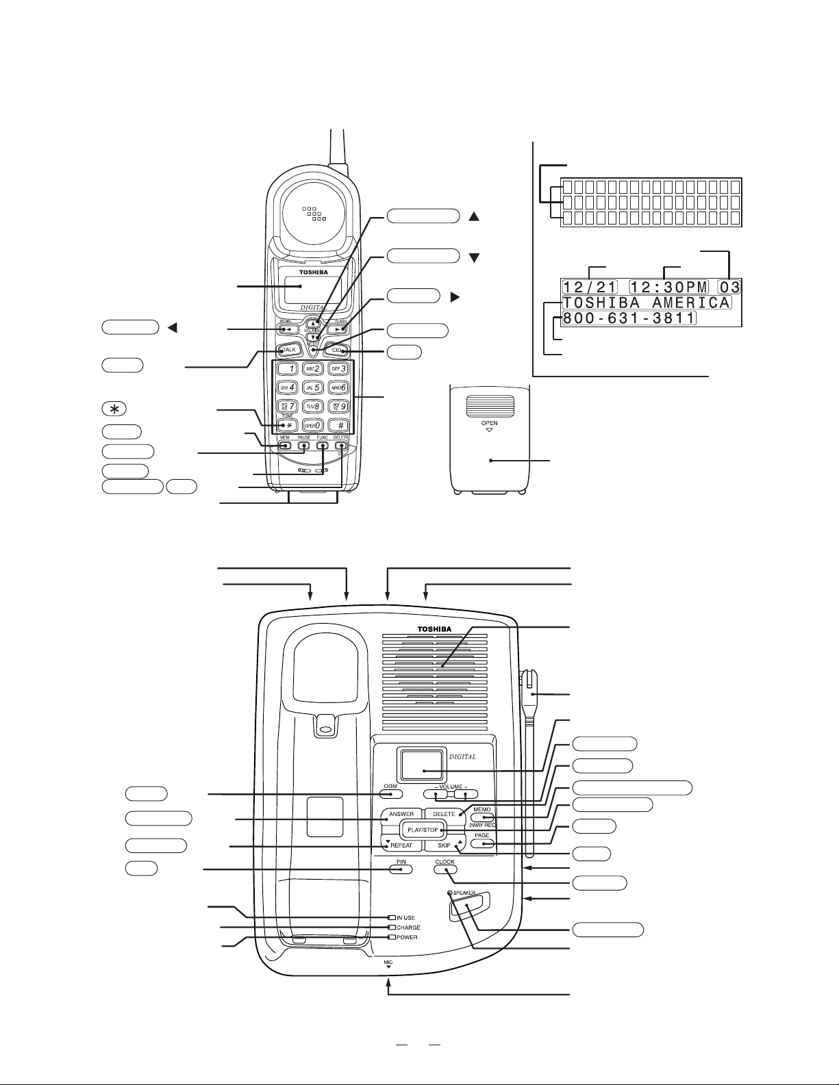
OPERATING CONTROLS
HANDSET CONTROLS AND FUNCTIONS LCD
Dot matrix display
VOL/RING ( ) button
(up arrow button)
VOL/RING ( ) button
Liquid Crystal Display
(LCD)
REDIAL ( ) button
(Left arrow button)
TALK button
(down arrow button)
FLASH ( ) button
(Right arrow button)
SELECT button
CID (Caller ID) button
Caller's telephone number
Caller's name
Number of calles
Date Time
(TONE) button
dialpad
MEM (Memory) button
PAUSE button
FUNC (Function) button
DELETE CH button
Charging contacts
BASE UNIT CONTROLS AND FUNCTIONS
DC in 9V Jack
TEL LINE Jack
900MHz
CALLER ID
FD-9839
OGM button
ANSWER button
REPEAT button
PIN button
IN USE LED
CHARGE LED
POWERR LED
Battery compartment
T-P (TONE-PULSE) switch
Ringer ON/OFF switch
Speaker
Antenna
LED Display
VOLUME button
DELETE button
MEMO/2WAY REC button
PLAY/STOP button
PAGE button
SKIP button
Rec Time Switch (ANN/4/1)
CLOCK button
Ring Time Switch (2/4/TS)
SPEAKER button
Speaker LED
Microphone
2
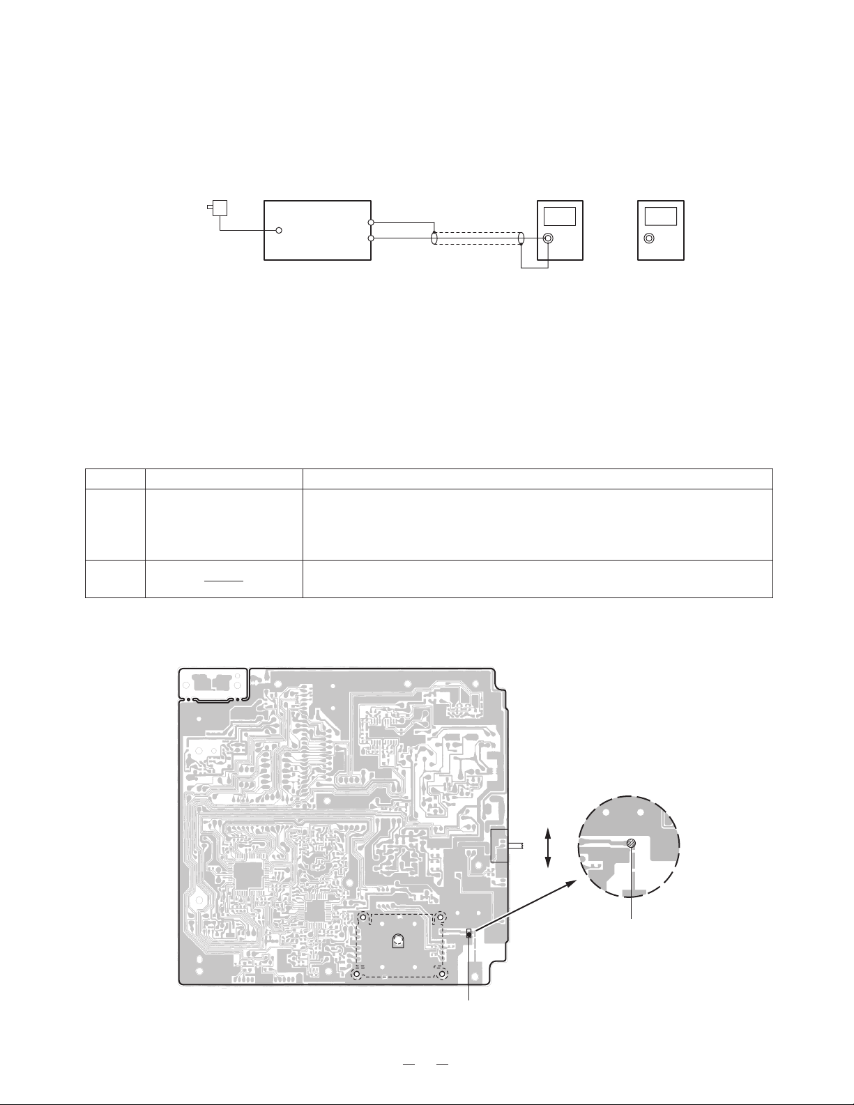
Base Unit
Transmitter Section
ALIGNMENT PROCEDURE
Connections
AC Adapter
(120V 60Hz)
BASE Unit
Test Point
(J1)
Spectrum Analyzer
FM Deviation Meter
Preset
a) Remove the solder on the pattern (refer to the illust. below).
b) Set the “TONE / PULSE” switch to PULSE.
c) Connect the AC adapter to the base unit while pressing the “PAGE” key, and keep pressing it continuously for
approximate 2 seconds.
d) Release the “PAGE” key when entering TEST mode 1 with CHARGE LED lighting.
Alignment Procedure
step
1
2
Adjustment
VR202
(TX P ower)
Remarks
Connect the Spectrum Analyzer to test point (J1).
Adjust VR202 so that the power instructions of the Spectrum analyzer reaches
-6.0dBm.
Then confirm the frequency is 926.295415 MHz.
Press the “PAGE” key twice and connect the FM Deviation Meter to test
point J1. Confirm the de viation is 23 ~ 46 kHz.
Alignment Point Location on Base Main PCB and Base RF PCB
Base Main PCB
S1
Base RF PCB
J1
VR202
Test Point
T
P
Remove solder
before alignment
3
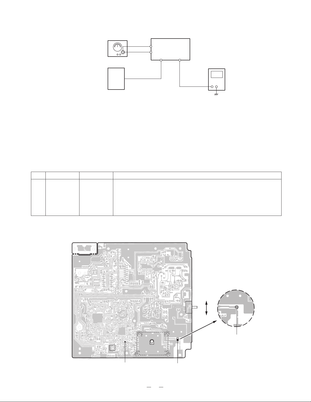
Receiver Section
Connections
AC 120V
60Hz
SG
+
9V Jack
AC
Adapter
Test Point
(J1)
DC IN
BASE Unit
Discriminator
Test Point
DC Voltmeter
Preset
a) Remove the solder on the pattern (refer to the illust. below).
b) Set the “T ONE/PULSE” switch to PULSE.
c) Connect the AC adapter to the base unit while pressing the “PAGE” key, and keep pressing it continuously for
approximate 2 seconds.
d) Release the “PAGE” key when entering TEST mode 1 with CHARGE LED lighting.
Alignment Procedure
step1Preset to
Adjustment
Remarks
Press the “PAGE” key for 3 times to enter the TEST Mode 4. Connect the
SG: 1mV
No modulation
L1
(Discriminator
Voltage)
RF Signal Generator to the test point (J1) on the Base MAIN PCB. Make
sure that the frequency is 903.417756 MHz.
Connect the DC Voltmeter to the Discriminator test point. Adjust L1 to
indicate DC 0.90 V.
Alignment Point Location on Base Main PCB and Base RF PCB
Base Main PCB
Base RF PCB
J1
L1
VR202
T
S1
P
Remove solder
before alignment
Discriminator Test Point
Test Point
4
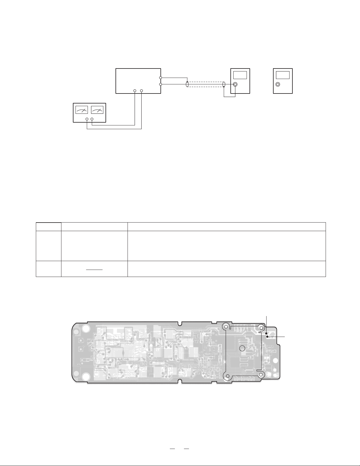
Handset Unit
Transmitter Section
Connection
Handset Unit
Test
Batt
Connector
DC Power Supply
3.8V
Point
(J601)
Preset
a) Remove the solder on the pattern (refer to the illust. below).
b) Connect DC power supply to battery connector on the handset unit.
c) Turn the DC power supply On while pressing “
∗∗
∗ ” and “ # “ keys, and keep pressing the keys continuously for
∗∗
approximate 2 seconds.
d) Release keys when entering TEST mode 1 with beep.
Alignment Procedure
step
1
2
Adjustment
VR502
Connect the Spectrum Analyzer to test point (J601).
Adjust VR502 so that the power instructions of the Spectrum analyzer reaches
-4.0 dBm.
Then comfirm the frequency is 903.617561 MHz.
Press the “3” key and connect the FM Deviation Meter to test point (J601).
Confirm the deviation is 23 ~ 46 kHz.
Spectrum Analyzer
Remarks
FM Deviation Meter
Alignment Point Location on Handset Main PCB and Handset RF PCB
Handset PCB
RF PCB
VR502
5
Test Point (J601)
Remove solder
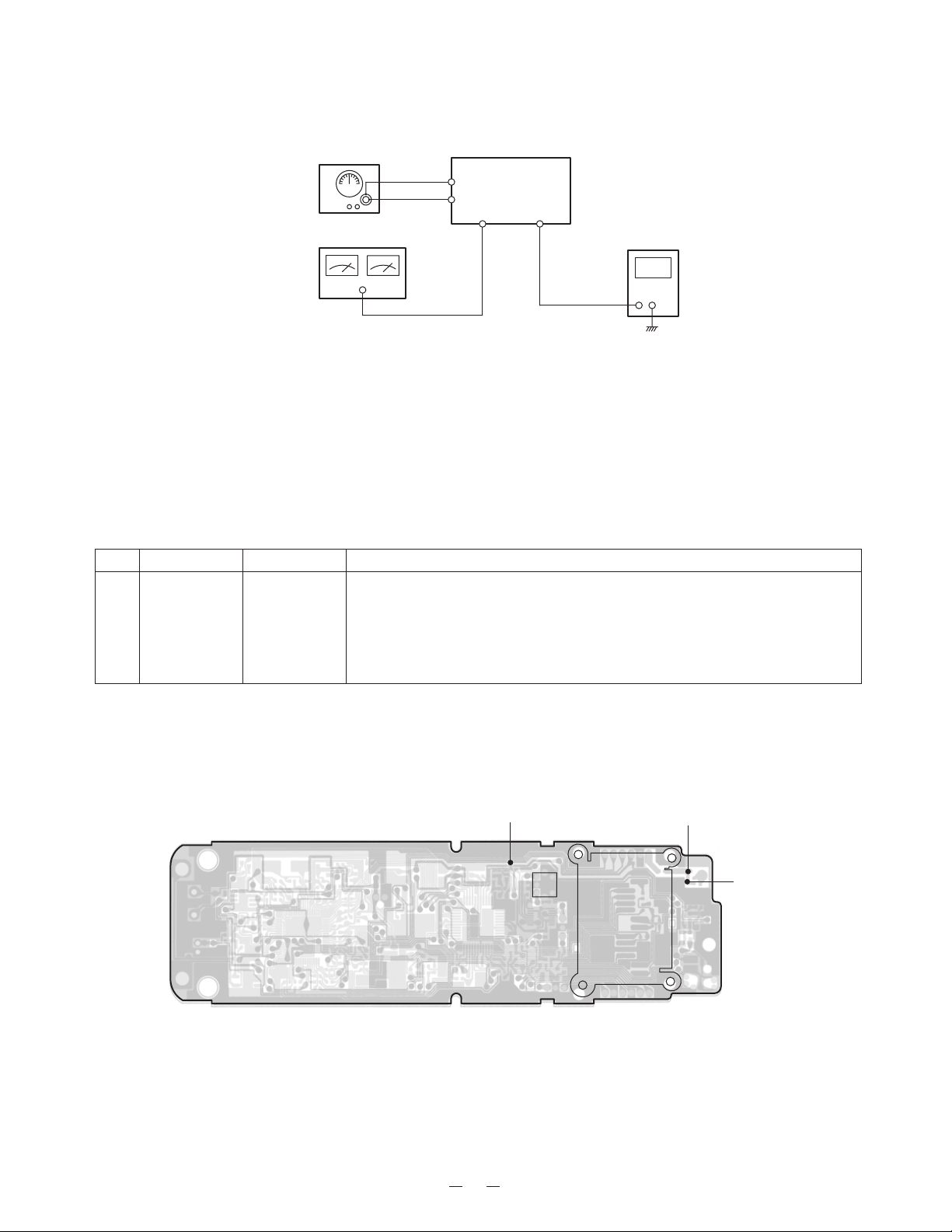
Receiver Section
Connections
RF SG
+
Test Point
(J601)
HANDSET Unit
DC Power Supply
Battery
Connector
DC 3.8V
Discriminator
Test Point
Preset
1) Remove the solder on the pattern (refer to the illust. below).
2) Connect DC power supply to battery connector on the handset unit.
3) Turn the DC power supply ON while pressing “
∗∗
∗ ” and “ # “ keys, and keep pressing the keys continuously for
∗∗
approximate 2 seconds.
4) Release keys when entering TEST mode 1 with beep.
Alignment Procedure
step1Preset to
SG: 1mV
No modulation
Adjustment
L603
(Discriminator
Voltage)
Press the “4” key to enter the TEST Mode 4. Connect the RF Signal
Generator to the test point (J601) on the handset MAIN PCB. Make sure
that the frequency is 926.495220 MHz.
Connect the DC Voltmeter to the Discriminator test point. Adjust L603 to
indicate DC 0.90 V.
DC Voltmeter
Remarks
Alignment Point Location on Handset Main PCB and Handset RF PCB
Handset PCB
Discriminator Test Point
RF PCB
L603
Test Point (J601)
Remove solder
6
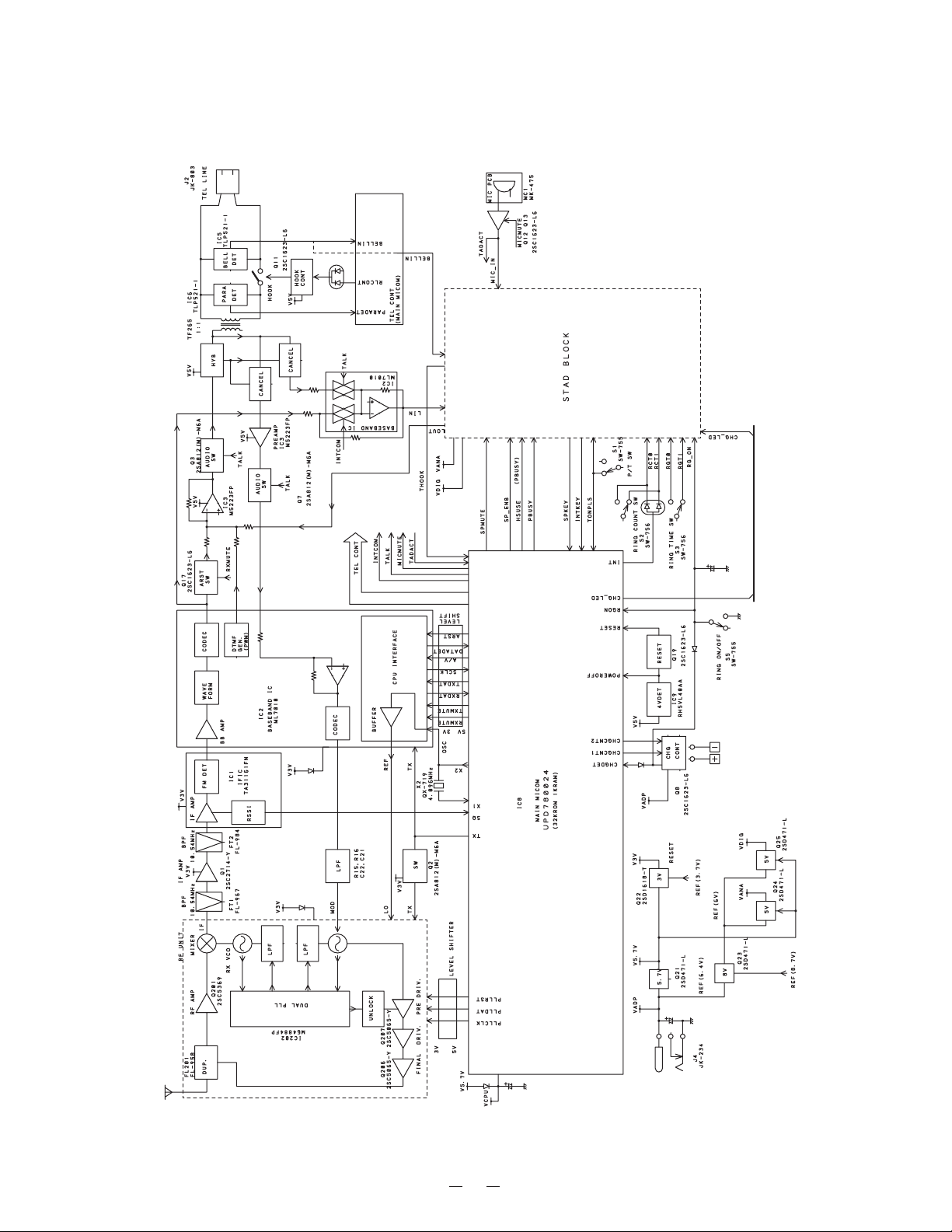
Base Unit, Main
BLOCK DIAGRAMS
7
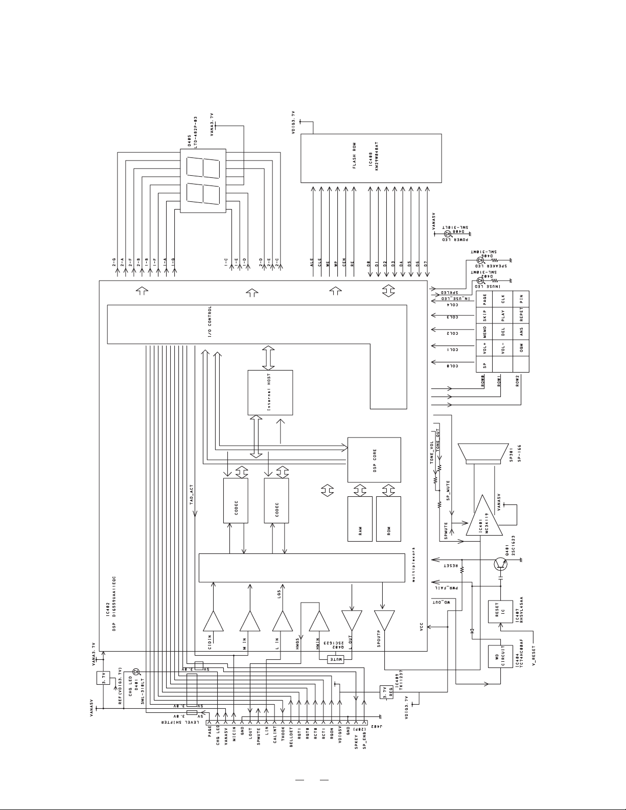
Base Unit, Key
8
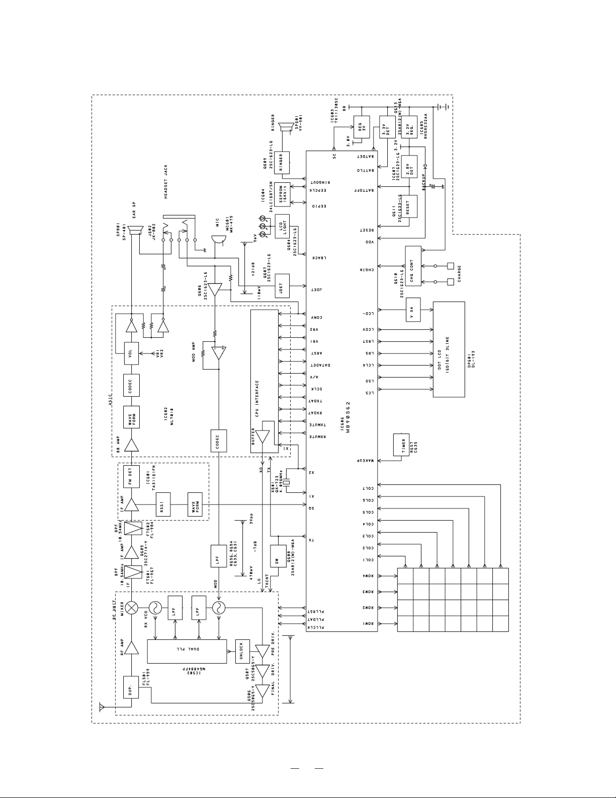
Handset
9
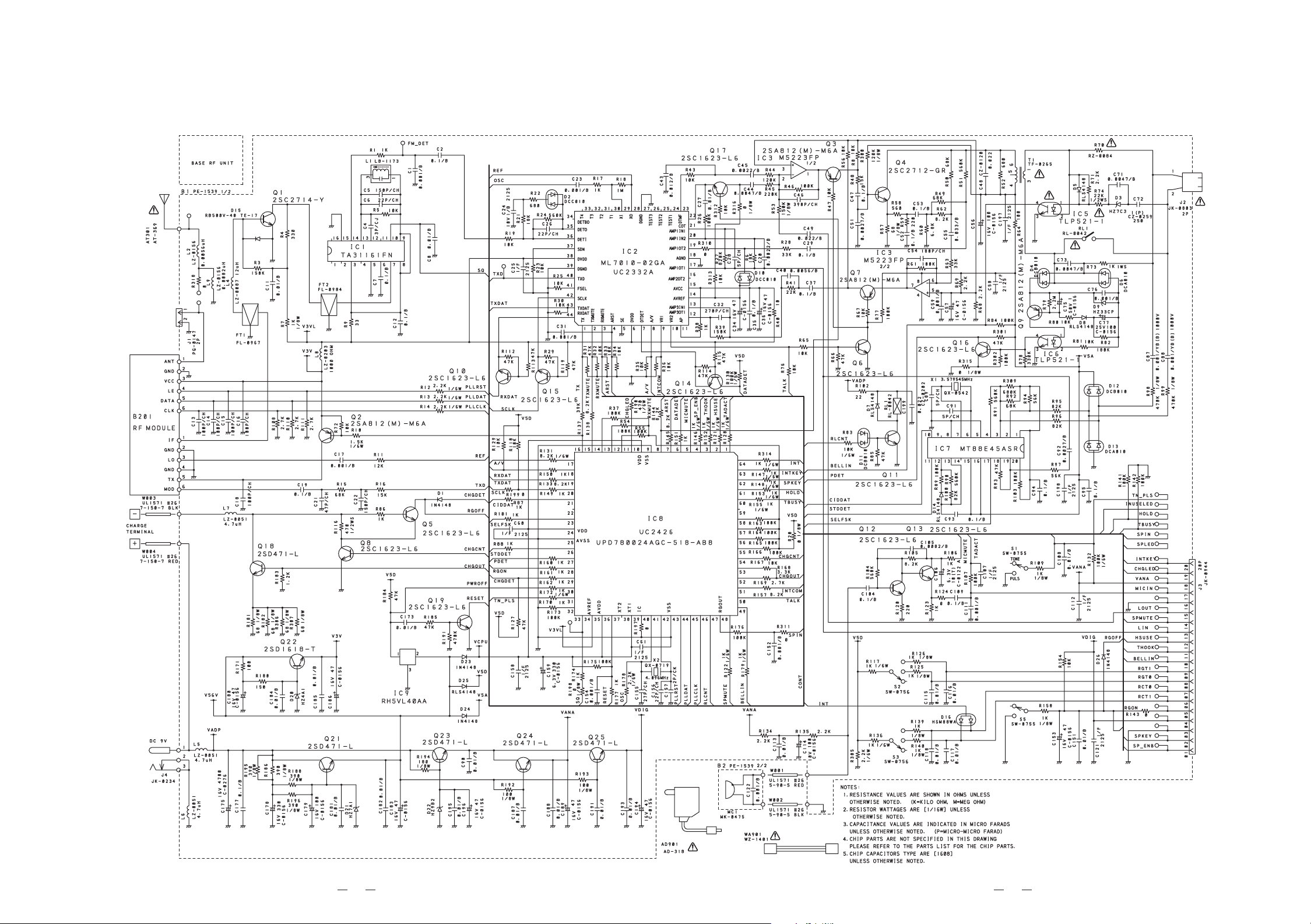
Base Unit, Main
SCHEMATIC DIAGRAMS
10
11
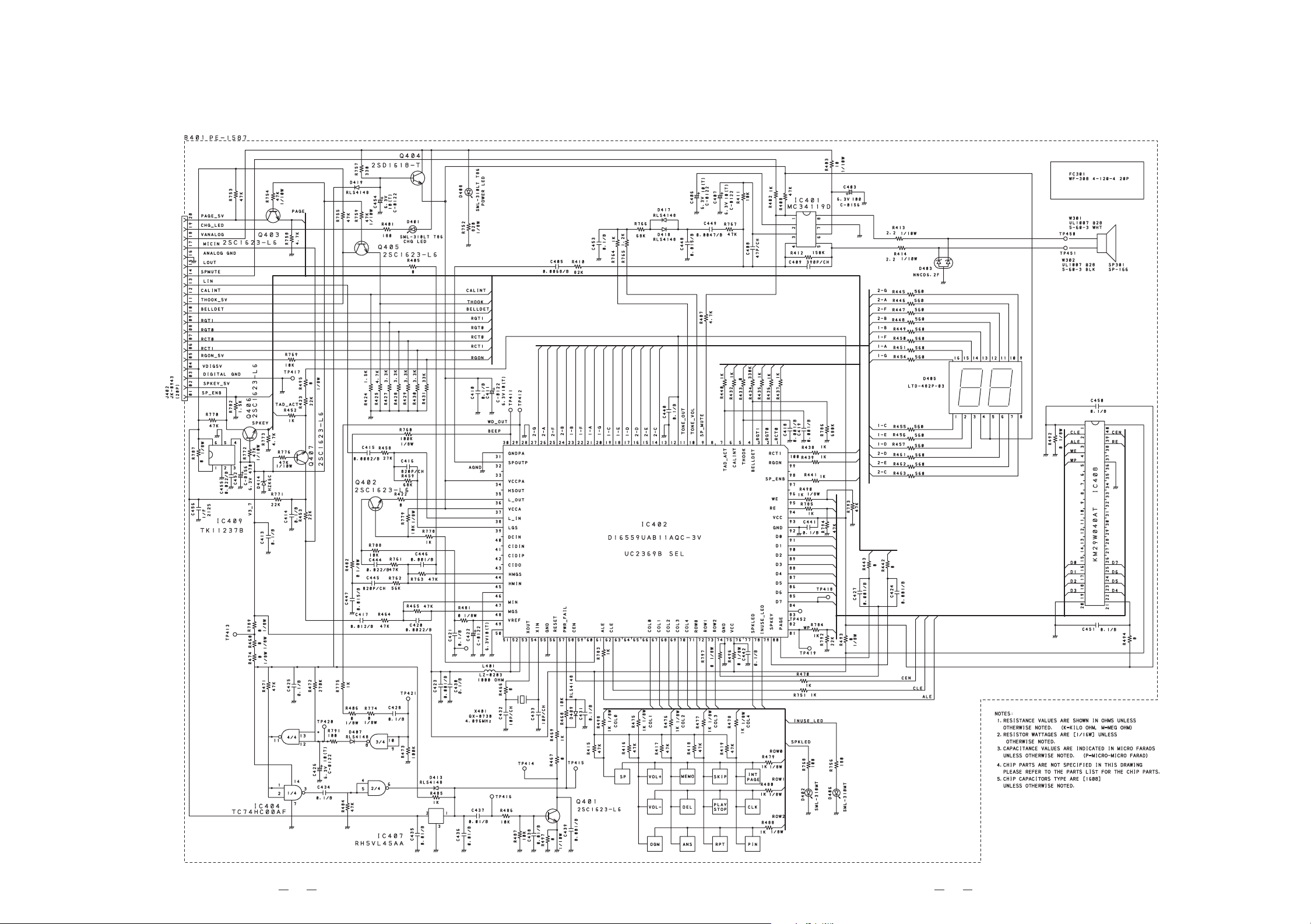
Base Unit, Key
12
13
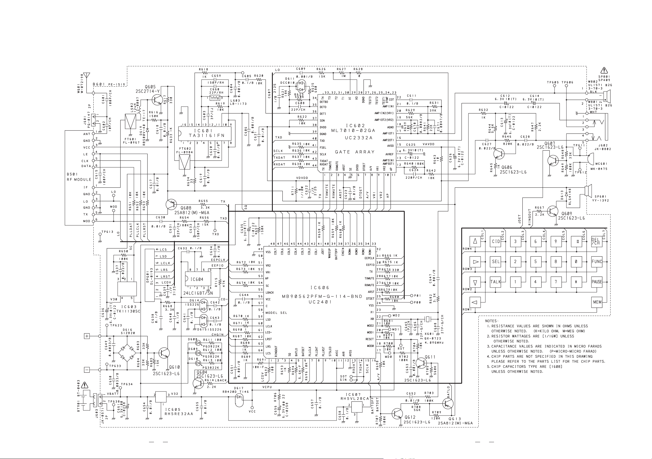
Handset
14
15
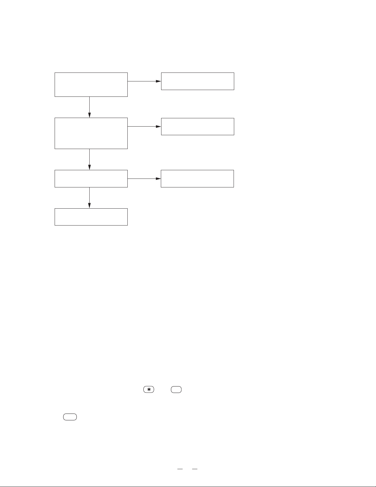
TROUBLESHOOTING HINTS
1. The bell does not ring.
When the PAGE SW of the
base is pressed, does the
ringer on the handset ring?
When the TEL SG is joined
with the base to make bell
signal, is there pulse wave at
pin 4 of IC5?
Is there pulse wave at
pin 49 of IC8?
Check IC8 and its
peripheral circuit.
BASE UNIT
OK
OK
OK
NG
NG
NG
See 2. The bell does not ring
& page does not ring.
Check IC5 and TEL network
circuit.
Check R179.
If you want to reset the unit to the factory settings
You can cancel the OGM, PIN, and the clock settings by the following process.
1) Disconnect the AC adaptor and telephone line cord from the base. Keep the A C adaptor connected to the wall
outlet. Make sure that the telephone line cord remains disconnected during this procedure.
2) While pressing the DELETE button, plug the AC power adaptor into the base. Keep pressing the DELETE
button for more than 4 seconds .
A beep sounds and “ P” blinks in the LED display.
To resume using the unit, connect the telephone line cord and place the handset on the base.
Note:
If you turn on the unit again, “ P” may flash.
HANDSET
Deletion of the Caller ID memory
To delete the Caller ID memory in the EEPROM, proceed with the following process:
1) Connect the battery with pressing and # buttons, and keep pressing the buttons continuously for
approximate 2 seconds.
2) Release buttons when entering TEST mode with beep.
3) Press CID button.
4) A confirmation beep will sound after about 8 seconds, then the data for caller ID is deleted.
(Note: Do not disconnect the battery until you hear the confirmation beep, otherwise the data may not be
completely deleted.)
16
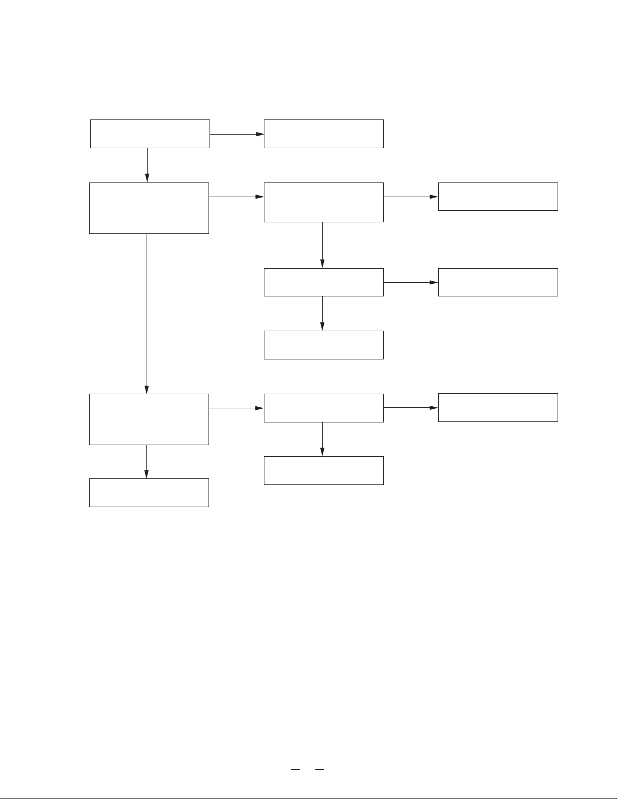
2. The bell does not ring & page does not ring.
Can the base and handset be
connected?
OK
Press handset DIAL key
while in TALK MODE.
Can key touch sound be
heard from the ringer?
OK
When the PAGE SW of the
base is pressed, does pin63
of IC8 change from high to
low?
NG
NG
NG
See 3. The base and handset
cannot be connected.
When the key of the handset is
pressed, can the pulse output
at pin 2 of IC606 be seen?
OK
At the Q609 collector, can the
pulse wave be seen?
OK
Check RINGER Y601.
Check R147, R753, R758,
R443, R754, C427 and Q403.
OK
NG
NG
NG
Check IC606.
Check R667 and Q609.
Replace defective part(s).
OK
Check IC8 and its peripheral
circuit.
Check IC402 and key circuit.
17
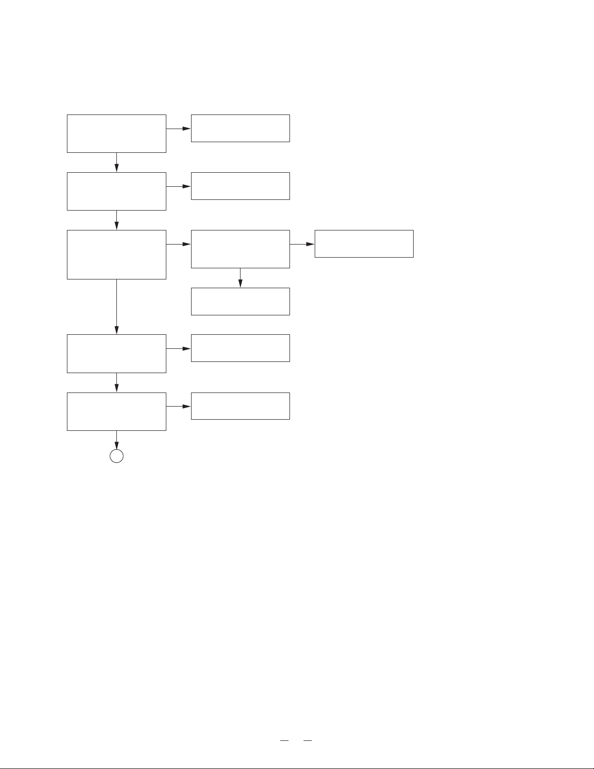
3. The base and handset cannot be connected.
Check whether the base
is able to set in the test
mode 1.
OK
Check the TX POWER
and the TX FREQUENCY
on the base unit.
OK
Press “PAGE” key twice,
check whether deviation
of the TX data is app . ±23
kHz~±46kHz Dev.
OK
Check whether the
handset is able to set in
the test mode 1.
OK
Check the TX POWER
and the TX FREQUENCY
on the handset unit.
OK
NGACheck IC4 and its
peripheral circuit.
NG
Check base RF unit.
Check whether there is a
NG
pulse data waveform at
C19.
OK
Check base RF unit.
NG Check IC606 and its
peripheral circuit.
NG
Check handset RF unit.
Check IC2, Q2 and the
NG
peripheral circuit.
18
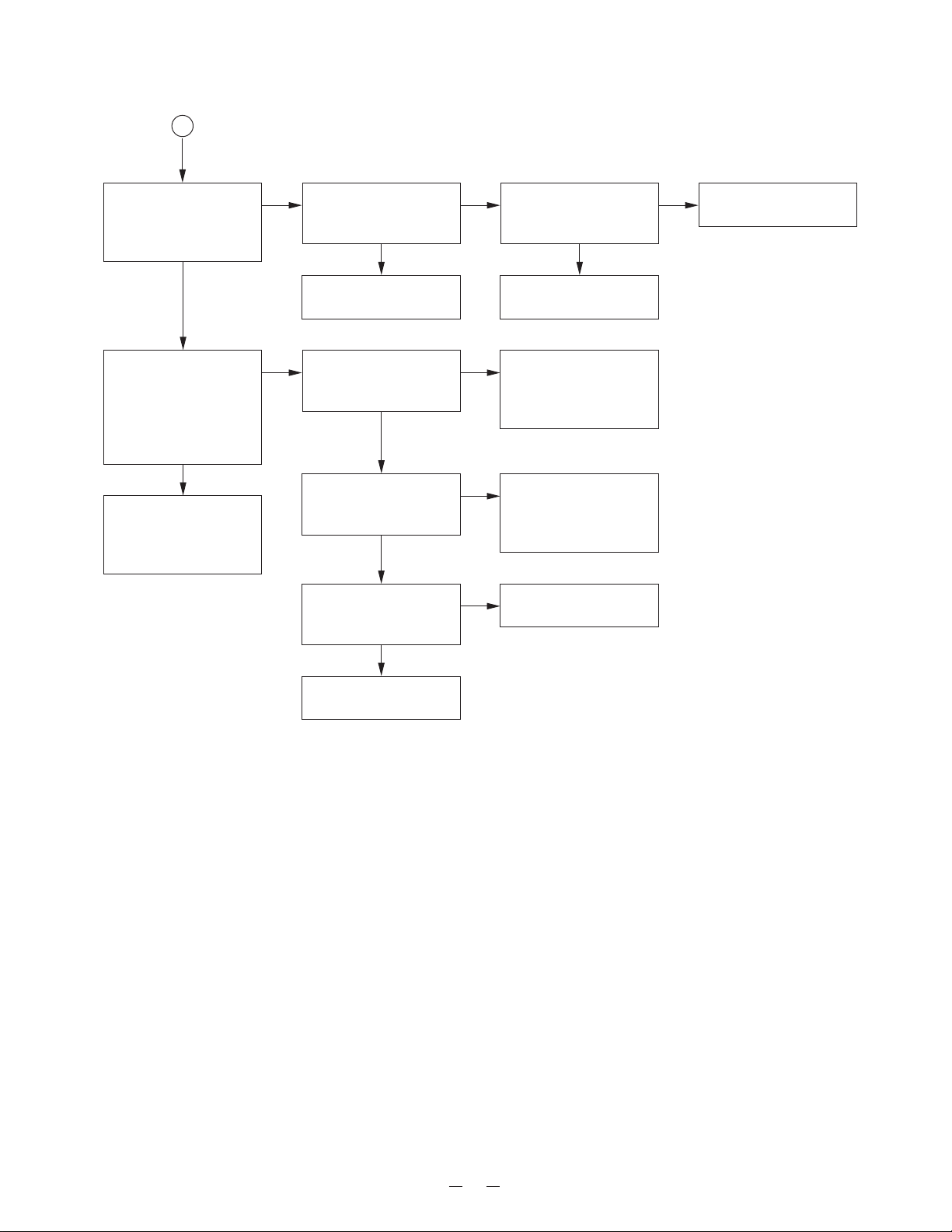
A
Press “3” key, check
whether deviation of the
TX data is app. ±23kHz
~ ±46kHz Dev.
OK
Press “5” ke y, 926.49522
MHz (30kHz ±30kHz
Dev.) 1mV output signal
from RF jack is applied.
Check whether the bell
ring.
OK
Place the handset on the
base to charge about 10
seconds, then connect
again.
NG Check whether there is a
pulse data waveform at
C630.
OK
Check handset RF unit.
NG Check whether there is
the 30kHz waveform at
C605.
OK
Check whether there is a
30kHz pulse wavef orm at
pin 35 of IC602.
OK
Check whether the
voltage at pin 10 of IC601
is more than 1V.
OK
Check whether there is
NG
a pulse data waveform at
pin 40 of IC602.
Check R656, C633,
R654, C631 and C630.
Check handset RF unit
NG
and the peripheral circuit
of IC601, Q605, FT601,
FT602.
Check R620, R621,
NG
R623, R625, C605, C607,
C608, D611, IC602 and
their peripheral circuit.
Check IC601 and its
NG
peripheral circuit.
OK
Check IC602 and its
NG
periperal circuit.
Check C606, IC606 and
its peripheral circuit.
19
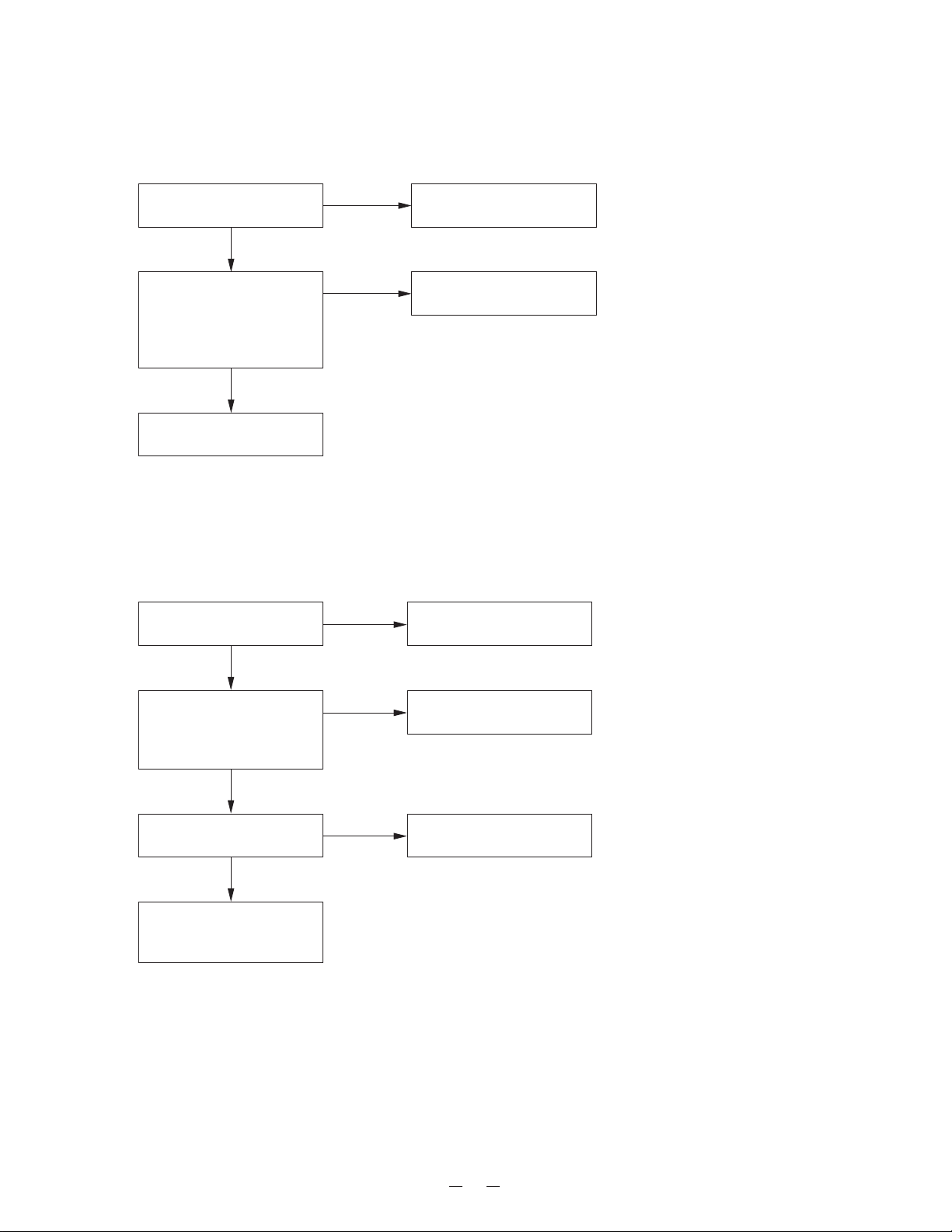
4. Cannot make a phone call (pulse).
Can the base and handset
be connected?
OK
While in TALK MODE, press
dial key of the handset.
Check whether square
waveform from pin 46 of IC8
is fed.
OK
Check R83, D11, Q11, RL1
and the peripheral circuit.
NG
NG
See 3. The base and handset
cannot be connected.
Check IC8 and its peripheral
circuit.
5. Cannot make a phone call (tone).
Can the base and handset be
connected?
OK
NG
See 3. The base and handset
be cannot be connected.
While in TALK MODE, press
dial key of the handset.
Can tone waveform from Pin
23 of IC2 is fed?
OK
Can tone signal be heard
from the handset speaker?
OK
Check the base TEL-line
circuit and RELAY control
circuit.
NG
NG
Check IC2 and its peripheral
circuit.
Check IC3, Q3, Q4 and the
peripheral circuit.
20
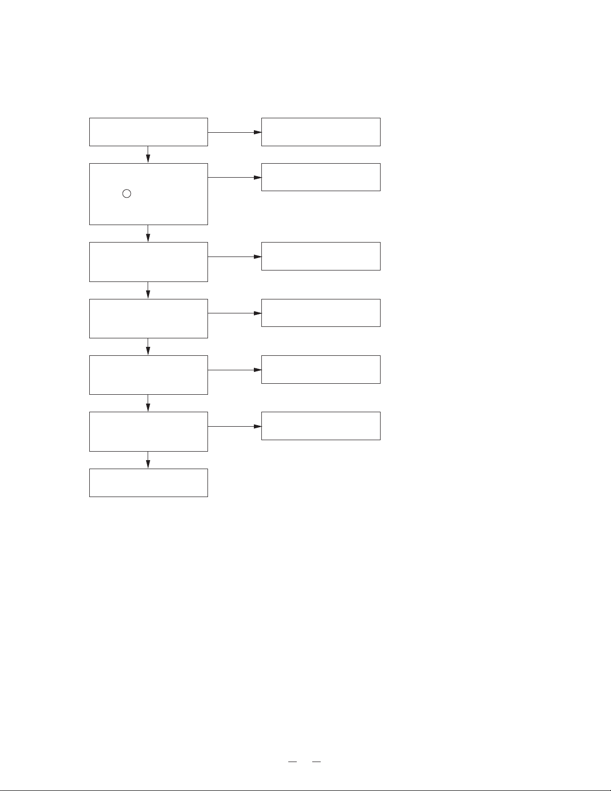
6. Voice cannot be transmitted to other party (outgoing call).
Can the base and handset be
connected?
OK
The 1 kHz, 3.3mV sine
waveform is applied to
+
MC601
sine waveform from collector
of Q606 be fed?
Check whether there is the
1 kHz sine waveform at pin
12 of IC602.
Check whether there is the
1 kHz sine waveform at pin
22 of IC2.
Check whether there is the
1 kHz sine waveform at the
Q4 collector.
side, can the 1 kHz
OK
OK
OK
OK
NG
NG
NG
NG
NG
See 3. The base and handset
cannot be connected.
Check Q606 and its
peripheral circuit.
Check IC602 and the
peripheral circuit.
Check IC2 and the peripheral
circuit.
Check IC2, Q4 and the
pripheral circuit.
Check whether the 1 kHz sine
waveform from TEL-line
output is fed.
OK
Check MC601 of handset.
NG
Check T1, RL1 and their
pripheral circuits.
21
 Loading...