

Page 1
BSI(Service Note) TOSHIBA
TOSHIBA TEC CORPORATION
2-4-1, Shibakoen, Minato-ku, TOKYO, 105-8524 JAPAN
BSI No
F99E624
SUBJECT
How to Make the Senior Main CPU ROM
MODEL
CATEGORY
Treatment in the field
----
CONTENT
The procedure for making the senior CPU is shown in this BSI.
Using ROM writer and jig
ROM writer :Minato electronics MODEL 1930 + SU 3000L / SU 3000LX or
Jig No. for
FROM
Blank ROM
No.
DP2460
FIELD APPLICATION
To be applied when necessary
FACTORY APPLICATION
Minato electronics MODEL 1881
:4408682340
:4402952200
Date
UNIT
Software
99/05/25
----
How to make the ROM when MODEL 1930 is used
Connect the ROM writer with a PC (MS-DOS) by cable (parallel comforming to CENTRONICS). 1.
Place the distribution data file on the HD of the connected PC.
Set as follows after the power supply of the ROM writer has been turned ON.2.
Device LH28F016
cdDB25
Vpp=5.00V 10us
Address mode 8bits x 1
Format MOTOROLA S
* Refer to BSI No. F98G343 about the device and format setting
procedure.
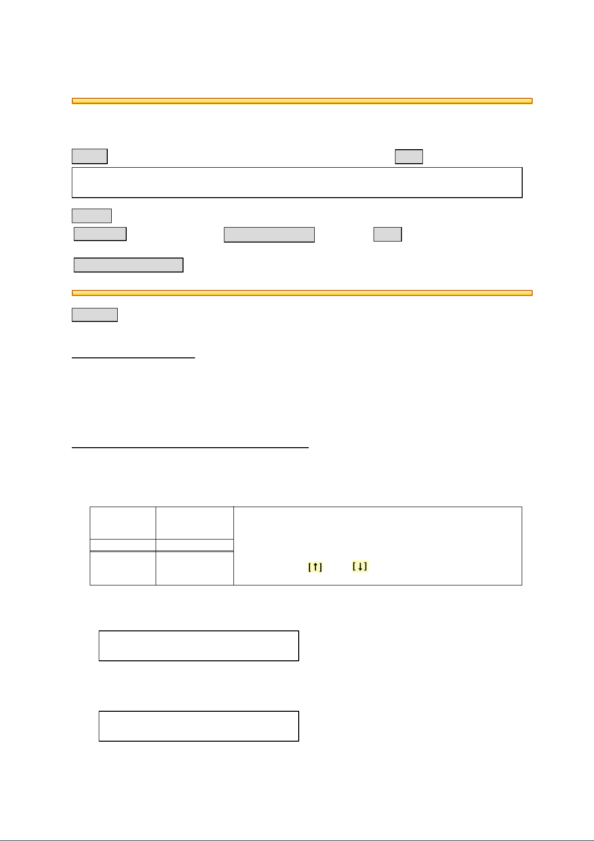
* Address mode setting procedure is shown below.
1. Push down the [MODE] key once.
2. Push down the [DEVICE] key once.
3. Push down the
4. Push down the [ENT] key once.
key or key and select "8bits x 1".
The ROM writer memory formatting is shown as follows.3.
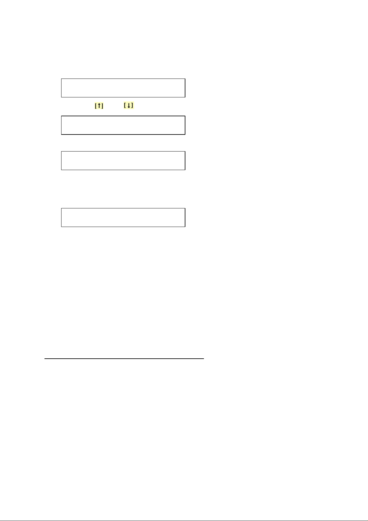
1. Push down [MODE] key till the following is displayed on the LCD.
SUB SELECT [ENT]
RAM INITIALIZE
2. Push down [ENT] key once.
3. Push down the [START] key once (formatting starts).
4. Pushing down [RESET] key once after the following display.
RAM INITIALIZE
COMPLETE
IC1 distribution data (identification end is "1" file) are transferred to the ROM writer memory as 4.
Page 2
BSI No. F99E624 Page 2
follows.
1. Start the PC (MS-DOS) -> Change the current directory to the directory which has distribution
data.
2. Push down till the LCD display is as follows.
SUB SELECT [ENT]
I/O Rs Input
3. Push down key or till the LCD display is as follows.
SUB SELECT [ENT]
I/O Pr Input
4. Push down the [ENT] key once (The LCD displays as follows.).
PRIN MOTOROLA
000000 000000
5. Push down [START] key once (change to data transfer standby from PC).
6. Start the following command on the PC (data transfer starts.).
copy (transfer data file) prn:
7. When the data transfer is finished normally, the following is displayed on the LCD.
PRIN MOTOROLA
COMPLETE
The data on the memory of the ROM writer are written to the blank ROM IC1. Then, the 5.
procedure should be performed as in BSI NO. F98G343 [writing (M1930 -> blank ROM)]. When it
is finished normally, "check sum" is displayed on the LCD. (SUM: XXXX is displayed.). Make sure
to check that the value corresponds with the transfer data check sum (write to ROM transfer
sheet). When the ROM in which the data are inputted is used again, the current data are cleared
and new ones should be inputted. For details of the data erasure procedure, refer to BSI NO.
F98G343.
Format the ROM writer memory again.6.
The IC2 transfer data (identification is "2" file.) are transferred to the ROM writer memory. The 7.
procedure is the same as for IC1.
The data on the ROM writer memory are written to the blank ROM IC2. The procedure is the 8.
same as for IC1.
How to make the ROM when the MODEL 1881 is used.
Connect the ROM writer by cable with a PC (Windows) (parallel conforming to CENTRONICS). 1.
The connecting PC needs to have ROM writer control software installed and data transferred to
the HD.
The PC starts (Windows) as does start the ROM writer control software. The following procedure 2.
is for the control software.
Set the device. The procedure is shown as below.3.
1. Left-click the [Select] key.
2. Select from "Vendor" to "SHARP" and from "Device" to "LH28F016SU @56" in the "Select
Device" Window.
Load the IC1 transfer data as follows.4.
Page 3

BSI No. F99E624 Page 3
1. Left-click the [Load] key.
2. After "File open" is displayed, select the IC1 transfer data file.
3. The "Load A File To Buffer" Window is displayed so set as follows.
Auto Format
Detected
From File Mode : Normal
To Buffer Mode : Normal
From File Address : 0
To Buffer Address : 0
Buffer Size : 200000
Clear buffer
Options
The blank ROM is installed on the jig which is set on IC1 and installed in the ROM writer socket. 5.
For the method of setting the jig, refer to BSI No. F98G343.
When the ROM in which the data are inputted is to be used again, click the [Erase] key and the 6.
current IC1 data should be cleared.
Write the memory buffer data to the blank ROM IC1 as follows.7.
1. Left-click the [Prog] key ( data writing starts.).
2. Make sure to that the lower 4 figures of "check sum" value correspond with the transfer data
check sum.
Format the memory buffer as follows.8.
: Motorola S
: Blank state
1. Left-click the [Edit] key.
2. The "Buffer Edit" window is displayed so left-click [Fill] key.
3. The "Buffer Fill" window is displayed, set as below and left-click the [OK] key.
From
Address
To Address : 1fffff
Code (HEX) : ff
Load the IC1 transfer data to the memory buffer. The procedure is same as for IC1.9.
Install the blank ROM to the jig, set the it to the IC2 and install the ROM writer socket. For the 10.
method of jig setting, refer to BSI No. F98G343.
When the ROM in which the data are inputted to be used again, left-click the [Erase] key and the 11.
current IC2 data should be cleared.
Write the memory buffer data to blank ROM IC2 in the same way as for IC1.12.
: 0
 Loading...