

Page 1

This file is provided FREE OF CHARGE from the
electromaniacs.com community
You are free to distribute this file to other persons
who needs it , but without of charge
Also on
thousands of service manuals , schematics free of
charge
http://electromaniacs.com you can find
Page 2

SERVICE MANUAL
Plasma Display
50XP37C
FILE NO. 010-200328
50XP37E
50XP37F
50XP37H
Mar. 2004 (YC)
Page 3
50XP37
CONTENTS
Page Page
1 Applicable signals 3
2 Safety Precautions
2.1. General Guidelines
3 Prevention of Electro Static Discharge (ESD) to
Electrostatically Sensitive (ES) Devices
4 About lead free solder (PbF)
5 PCB Structure sheet of GPH6D2 chassis
6 Service Hint
7 Location of Lead Wiring
8 Adjustment Procedure
8.1. Driver Set-up
8.2. Initialization Pulse Adjust
8.3. P.C.B. (Printed Circuit Board) exchange
8.4. Adjustment Volume Location
8.5. Test Point Location
9 Service mode
9.1. CAT (computer Aided Test) mode
9.2. IIC mode structure (following items value is sample data.)
10 Alignment
10.1. 625i/625p panel white balance
10.2. PC/RGB panel white balance
10.3. HD panel white balance
11 Trouble shooting guide
11.1. Self Check
11.2. No Power (Power shut down)
11.3. No Picture
11.4. Local screen failure
12 Conductor Views
12.1. PF-Board
12.2. P-Board
12.3. HX-Board
12.4. HV-Board
12.5. HZ-Board
12.6. HT-Board
12.7. J-Board
12.8. D-Board
12.9. C1-Board
12.10. C2-Bo ard
12.11. C3-Bo ard
12.12. C4-Bo ard
12.13. C5-Bo ard
12.14. C6-Bo ard
12.15. SC-Bo ard
12.16. SU-Bo ard
12.17. SD-Bo ard
10
10
11
12
13
13
13
13
15
16
16
18
19
20
20
20
21
22
23
23
25
28
29
30
31
32
34
37
38
39
40
41
42
43
45
47
4
4
5
6
7
8
9
12.18. SS, SS2 and SS3-B oard
12.19. Z- Board
12.20. V1, S1 and H3-Bo ard
13 Replacementpanelhandlingprecautionsandreplacement
procedure
14 PartsLocation
15 Chassis and Cabinet Replacement Parts List
16 Specifications
Appendix
Block and Schematic Diagrams
48
50
51
55
57
59
END
– 2 –
Page 4
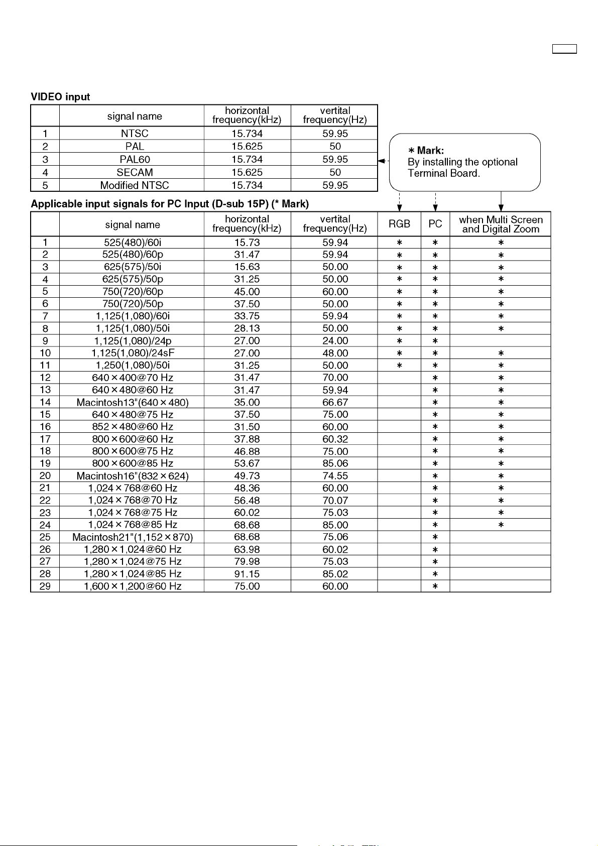
1 Applicable signals
50XP37
– 3 –
Page 5
50XP37
2 Safety Precautions
2.1. General Guidelines
1. When servicing, observe the original lead dress. If a short circuit is found, replace all parts which have been overheated or
damaged by the short circuit.
2. After servicing, see to it that all the protective devices such as insulation barriers, insulation papers shields are properly
installed.
3. After servicing, make the following leakage current checks to prevent the customer from being exposed to shock hazards.
2.1.1. Leakage Current Cold Check
1. Unplug the AC cord and connect a jumper between the two
prongs on the plug.
2. Measure the resistance value, with an ohmmeter, between
the jumpered AC plug and each exposed metallic cabinet
part on the equipment such as screwheads, connectors,
control shafts, etc. When the exposed metallic part has a
return path to the chassis, the reading should be between
1MW and 5.2MW.
When the exposed metal does not have a return path to
the chassis, the reading must be
.
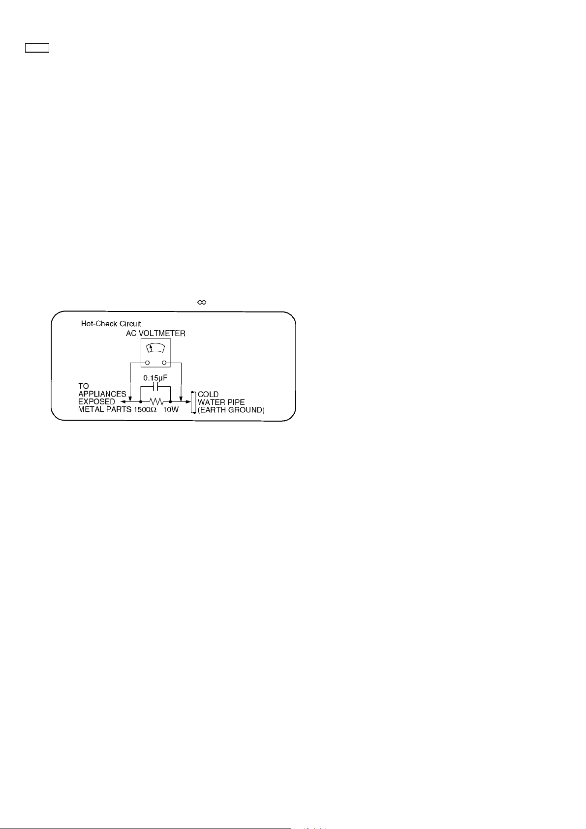
Figure 1
2.1.2. Leakage Current Hot Check (See
Figure 1.)
1. Plug the AC cord directly into the AC outlet. Do not use an
isolation transformer for this check.
2. Connect a 1.5kW, 10 watts resistor, in parallel with a 0.15µF
capacitors, between each exposed metallic part on the set
and a good earth ground such as a water pipe, as shown in
Figure 1.
3. Use an AC voltmeter, with 1000 ohms/volt or more
sensitivity, to measure the potential across the resistor.
4. Check each exposed metallic part, and measure the
voltage at each point.
5. Reverse the AC plug in the AC outlet and repeat each of the
above measurements.
6. The potential at any point should not exceed 0.75 volts
RMS. A leakage current tester (Simpson Model 229 or
equivalent) may be used to make the hot checks, leakage
current must not exceed 1/2 milliamp. In case a
measurement is outside of the limits specified, there is a
possibility of a shock hazard, and the equipment should be
repaired and rechecked before it is returned to the
customer.
– 4 –
Page 6
3 Prevention of Electro Static Discharge (ESD) to
Electrostatically Sensitive (ES) Devices
Some semiconductor (solid state) devices can be damaged easily by static electricity. Such components commonly are called
Electrostatically Sensitive (ES) Devices. Examples of typical ES devices are integrated circuits and some field-effect transistors and
semiconductor "chip" components. The following techniques should be used to help reduce the incidence of component damage
caused by electro static discharge (ESD).
1. Immediately before handling any semiconductor component or semiconductor-equipped assembly, drain off any ESD on your
body by touching a known earth ground. Alternatively, obtain and wear a commercially available discharging ESD wrist strap,
which should be removed for potential shock reasons prior to applying power to the unit under test.
2. After removing an electrical assembly equipped with ES devices, place the assembly on a conductive surface such as alminum
foil, to prevent electrostatic charge buildup or exposure of the assembly.
3. Use only a grounded-tip soldering iron to solder or unsolder ES devices.
4. Use only an anti-static solder removal device. Some solder removal devices not classified as "anti-static (ESD protected)" can
generate electrical charge sufficient to damage ES devices.
5. Do not use freon-propelled chemicals. These can generate electrical charges sufficient to damage ES devices.
6. Do not remove a replacement ES device from its protective package until immediately before you are ready to install it. (Most
replacement ES devices are packaged with leads electrically shorted together by conductive foam, alminum foil or comparable
conductive material).
7. Immediately before removing the protective material from the leads of a replacement ES device, touch the protective material
to the chassis or circuit assembly into which the device will be installed.
Caution
Be sure no power is applied to the chassis or circuit, and observe all other safety precautions.
8. Minimize bodily motions when handling unpackaged replacement ES devices. (Otherwise hamless motion such as the brushing
together of your clothes fabric or the lifting of your foot from a carpeted floor can generate static electricity (ESD) sufficient to
damage an ES device).
50XP37
– 5 –
Page 7
50XP37
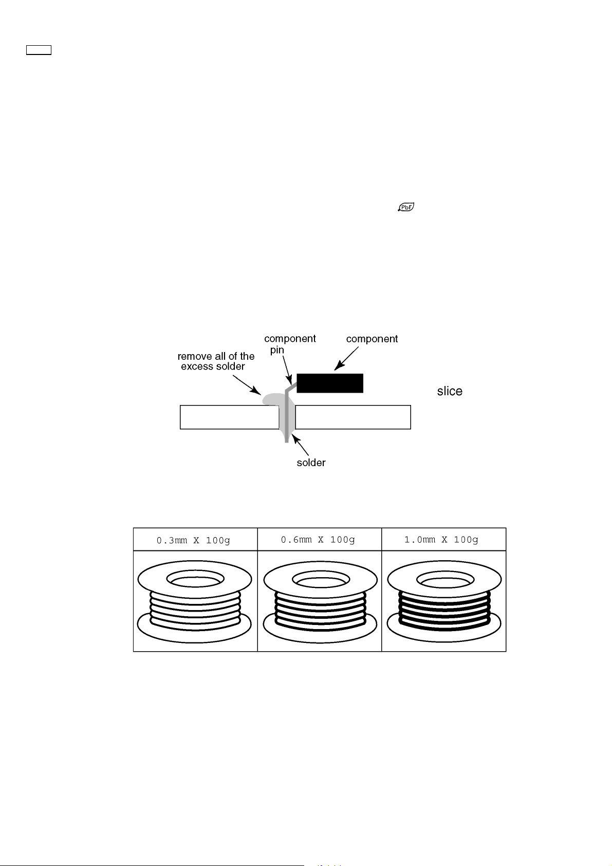
4 About lead free solder (PbF)
Note: Lead is listed as (Pb) in the periodic table of elements.
In the information below, Pb will refer to Lead solder, and PbF will refer to Lead Free Solder.
The Lead Free Solder used in our manufacturing process and discussed below is (Sn+Ag+Cu).
That is Tin (Sn), Silver (Ag) and Copper (Cu) although other types are available.
This model uses Pb Free solder in it’s manufacture due to environmental conservation issues. For service and repair work, we’d
suggest the use of Pb free solder as well, although Pb solder may be used.
PCBs manufactured using lead free solder will have the PbF within a leaf Symbol
Caution
· Pb free solder has a higher melting point than standard solder. Typically the melting point is 50 ~ 70 °F (30~40 °C) higher.
Please use a high temperature soldering iron and set it to 700 ± 20 °F (370 ± 10 °C).
· Pb free solder will tend to splash when heated too high (about 1100 °F or 600 °C).
If you must use Pb solder, please completely remove all of the Pb free solder on the pins or solder area before applying Pb
solder. If this is not practical, be sure to heat the Pb free solder until it melts, before applying Pb solder.
· After applying PbF solder to double layered boards, please check the component side for excess solder which may flow onto
the opposite side. (see figure below)
Suggested Pb free solder
There are several kinds of Pb free solder available for purchase. This product uses Sn+Ag+Cu (tin, silver, copper) solder.
However, Sn+Cu (tin, copper), Sn+Zn+Bi (tin, zinc, bismuth) solder can also be used.
stamped on the back of PCB.
– 6 –
Page 8
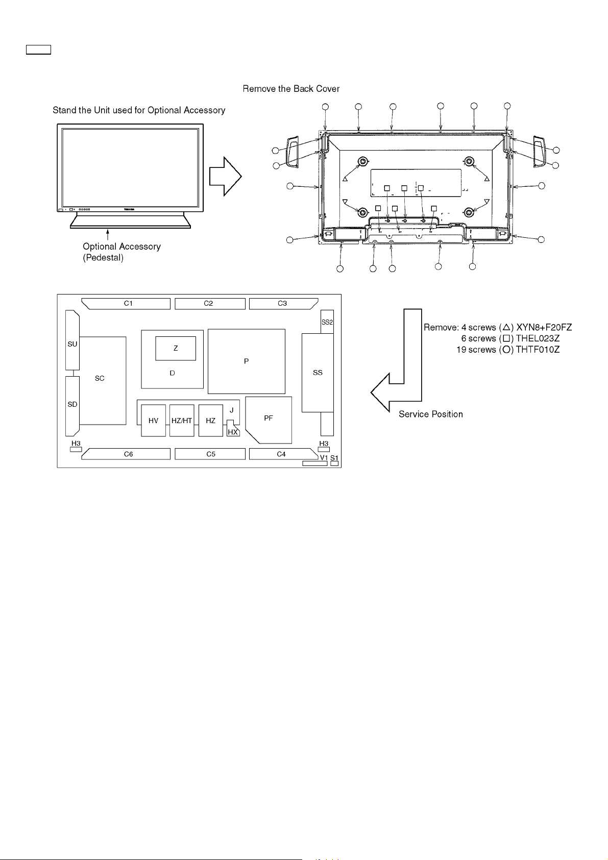
5 PCB Structure sheet of GPH6D2 chassis
Board Name Function Remarks
D Digital Signal Processor 1
J Slot Interface & SYNC processor 1
Z Audio out, DC-DC converter
SS Sustain Out 1
SC Scan out 1
SU Scan connection (Upper) 1
SD Scan connection (Lower) 1
C1 Data Drive (Upper Right)
C2 Data Drive (Upper Center)
C3 Data Drive (Upper Left)
C4 Data Drive (Lower Left)
C5 Data Drive (Lower Center)
C6 Data Drive (Lower Right)
H3 Speaker terminal
S1 Power switch
SS2 Sustain connection (Upper)
SS3 Sustain connection (Lower)
V1 Front SW. & Remote receiver
PF Line filter 1
P Power supply 1
HX PC_type_Input terminal
HZ (RTB033) RCA Component Video terminal
HV (RTB031) RCA Composite Video terminal
HT (RTB032) 21 Pin Scart terminal
50XP37
Remarks
1. Recommend PCB´s for initial service for GPH6D2 chassis.
– 7 –
Page 9
50XP37
6 Service Hint
SS3
– 8 –
Page 10
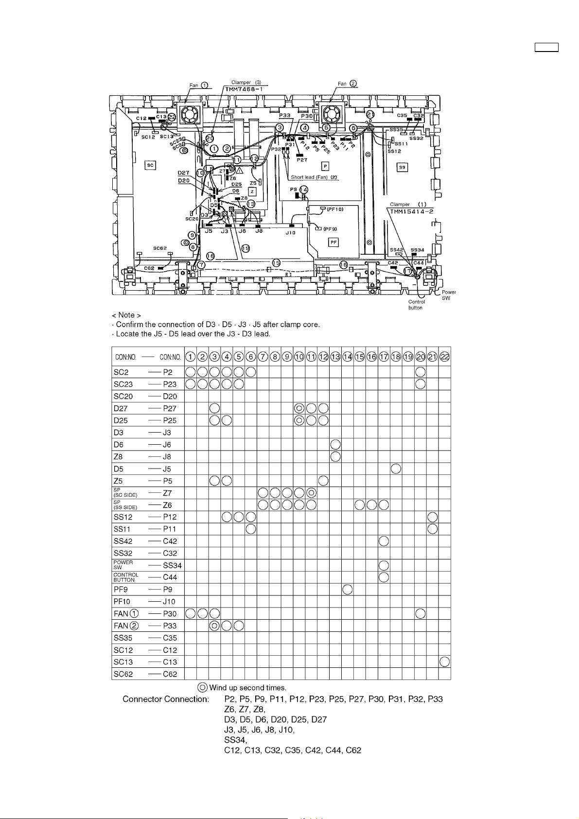
7 Location of Lead Wiring
50XP37
– 9 –
Page 11
50XP37
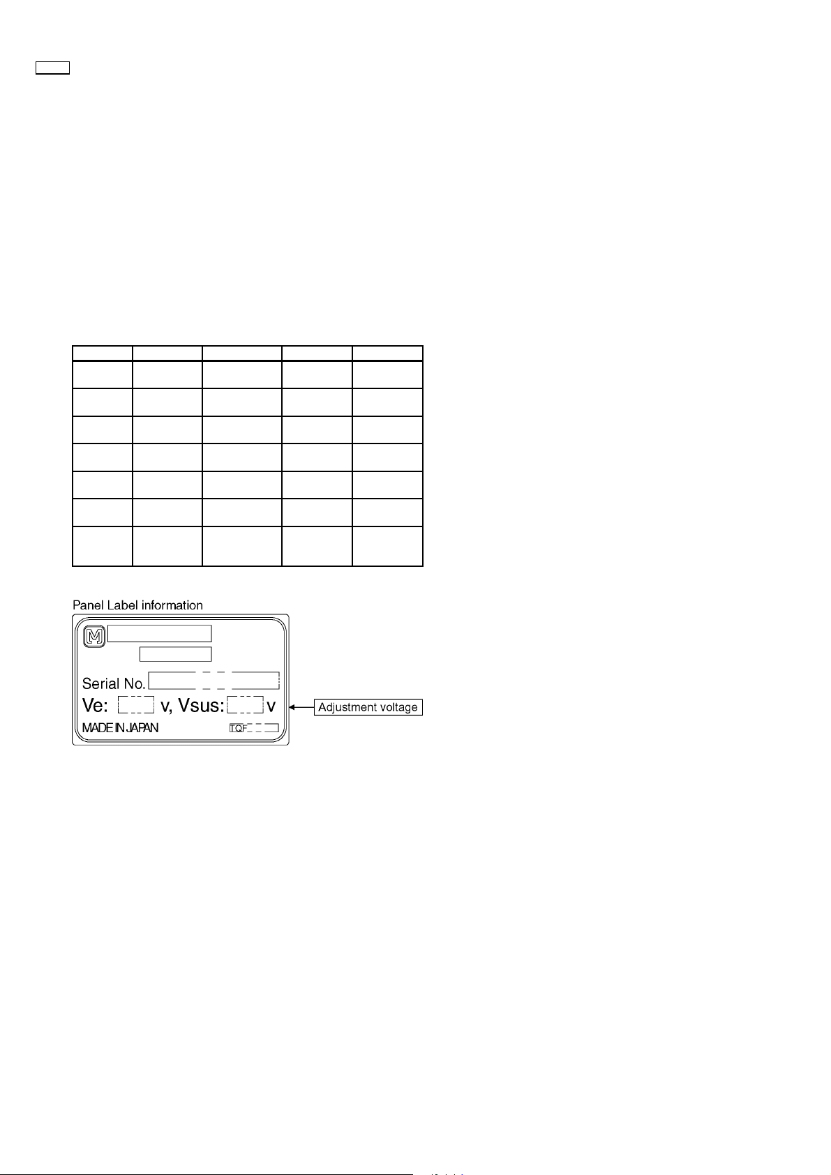
8 Adjustment Procedure
8.1. Driver Set-up
8.1.1. Item / Preparation
1. Input an APL 100 % white signal.
2. Set the picture controls: Picture mode: Normal
White balance: Cool
Aspect: 16:9
8.1.2. Adjustments
Adjust driver section voltages referring the panel data on the
panel data label.
Name Test Point Voltage Volume Remarks
Vsus TPVSUS
(SS)
Vbk TPVBK (SC) 140V ± 1V R6670 (SC) GND =
Vad TPVAD (SC) -85V ± 1V R6477 (SC) GND =
Ve TPVE (SS) Ve* ± 1V R6770 (SS) GND =
Vda TPVDA (SS) 75V ± 1V R665 (P) GND =
Vlow anode of
D540 (P)
PFC PR401 395V ± 0.5V R443 (P) Hot=PR401,
Vsus* ± 2V R641 (P) GND =
78V ± 0.1V R661 (P) GND =
chassis
chassis
chassis
chassis
chassis
chassis
Cold= W14
(wire)
*See the Panel label.
– 10 –
Page 12
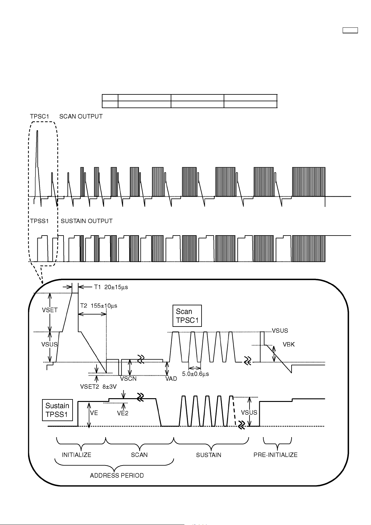
8.2. Initialization Pulse Adjust
1. Input a Cross hatch signal.
2. Set the picture controls: Picture mode: Normal
White balance: Cool
Adjust the indicated test point for the specified wave form.
Test point Volume Level
T2 TPSC1 (SC) R6557 (SC) 155 ± 10µ Sec
50XP37
– 11 –
Page 13
50XP37
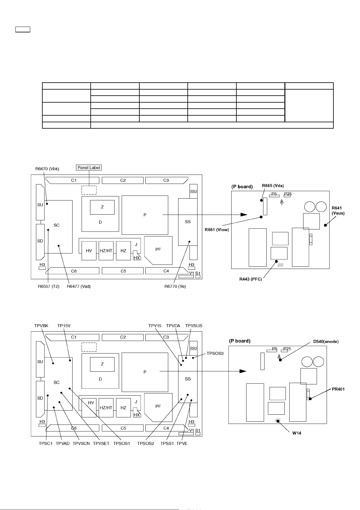
8.3. P.C.B. (Printed Circuit Board) exchange
8.3.1. Caution
1. To remove P.C.B. , wait 1 minute after power was off for discharge from electrolysis capacitors.
8.3.2. Quick adjustment after P.C.B. exchange
P.C.B. Name Test Point Voltage Volume Remarks
P Board Vsus TPVSUS (SS) Vsus* ± 2V R641 (P)
Vda TPVDA (SS) 75V ± 1V R665 (P)
SC Board Vad TPVAD (SC) -85V ± 1V R6477 (SC)
Vbk TPVBK (SC) 140 ± 1V R6670 (SC)
SS Board Ve TPVE (SS) Ve* ± 1V R6770 (SS)
D Board White blance
*See the Panel label.
8.4. Adjustment Volume Location
GND = chassis
8.5. Test Point Location
SS3
SS3
– 12 –
Page 14
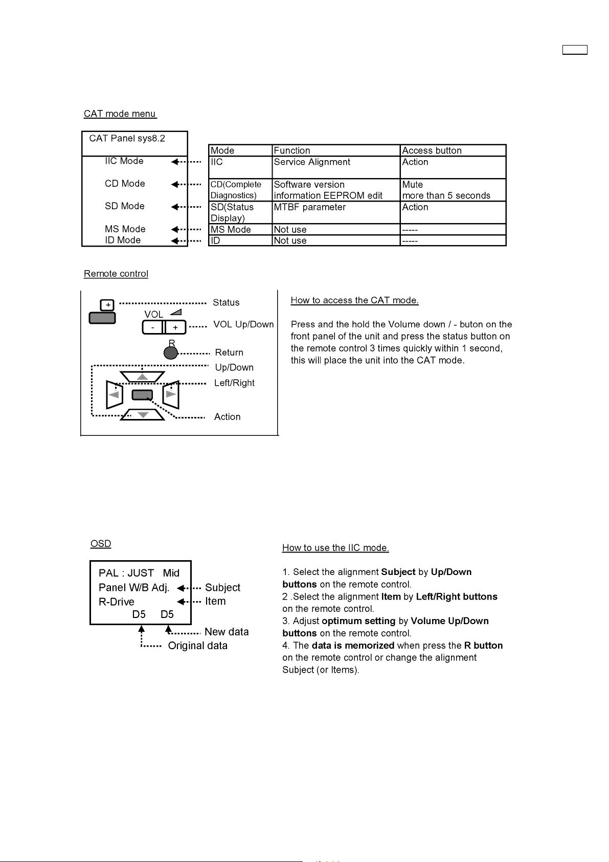
9 Service mode
9.1. CAT (computer Aided Test) mode
50XP37
To exit the CAT mode, access the ID mode and switch off the main power.
9.1.1. IIC mode
Select the IIC mode by Up/Down button on the remote control at the front page of CAT mode then press the Action button on
the remote control.
Subject and item are mentioned on page 16.
To exit the IIC mode, press the R button on the remote control.
– 13 –
Page 15
50XP37
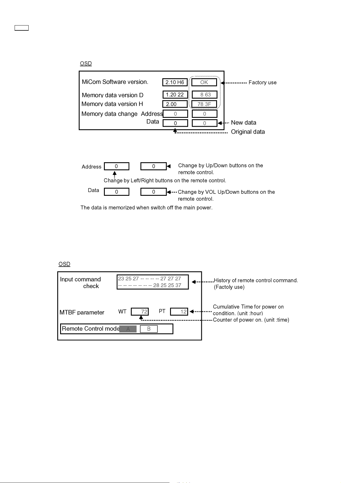
9.1.2. CD mode
Select the CD mode by Up/Down button on the remote control at the front page of CAT mode then press the Mute button on the
remote control more than 5 sec.
Micom software version (IC9705), this version can be upgrade by replacing of IC.
Memory data change
To exit the CD mode, press the R button on the remote control.
9.1.3. SD mode
Select the SD mode by Up/Down button on the remote control at the front page of CAT mode then press the Action button on the
remote control.
To exit the SD mode, press the R button on the remote control.
– 14 –
Page 16
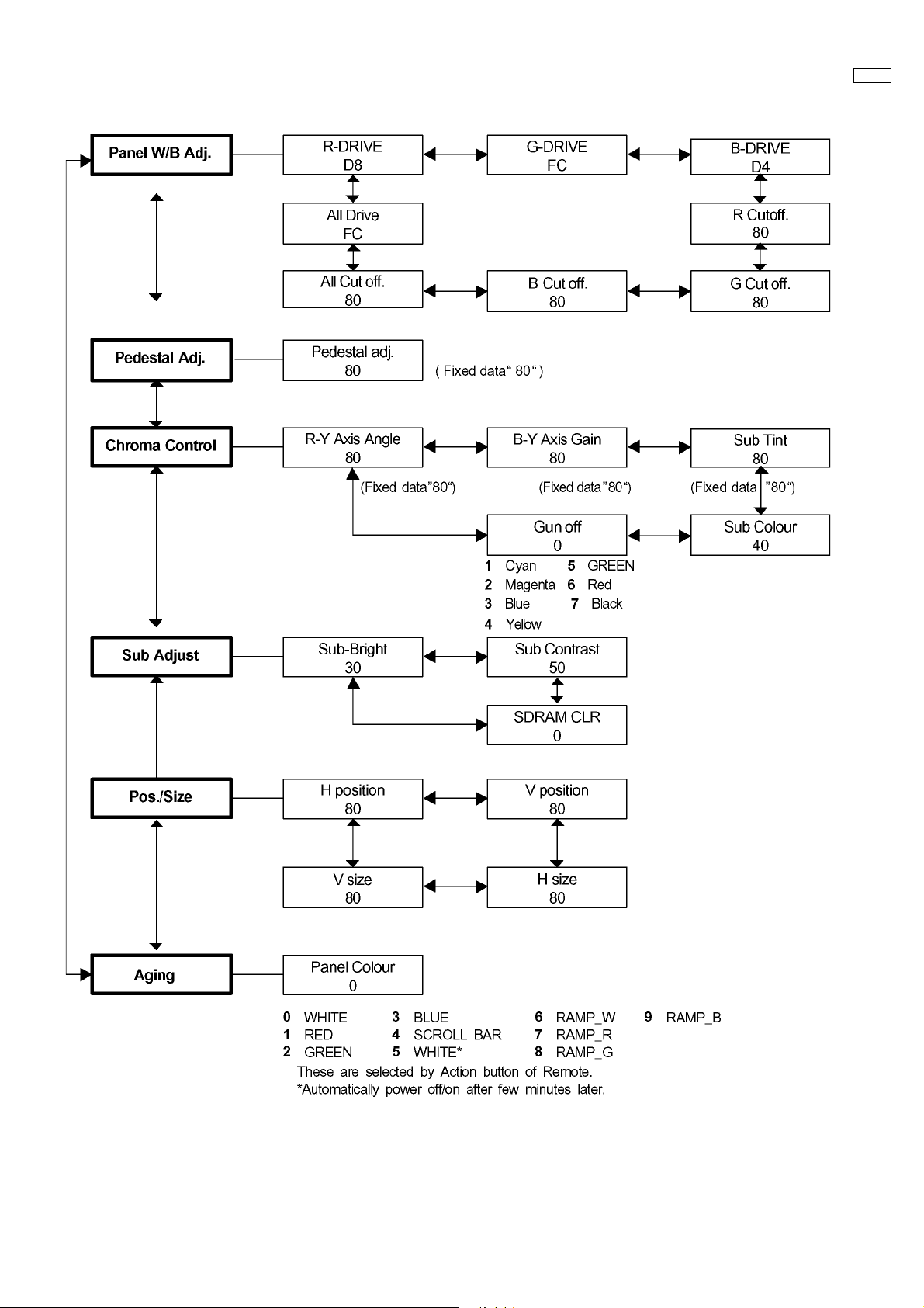
9.2. IIC mode structure (following items value is sample data.)
50XP37
– 15 –
Page 17
50XP37
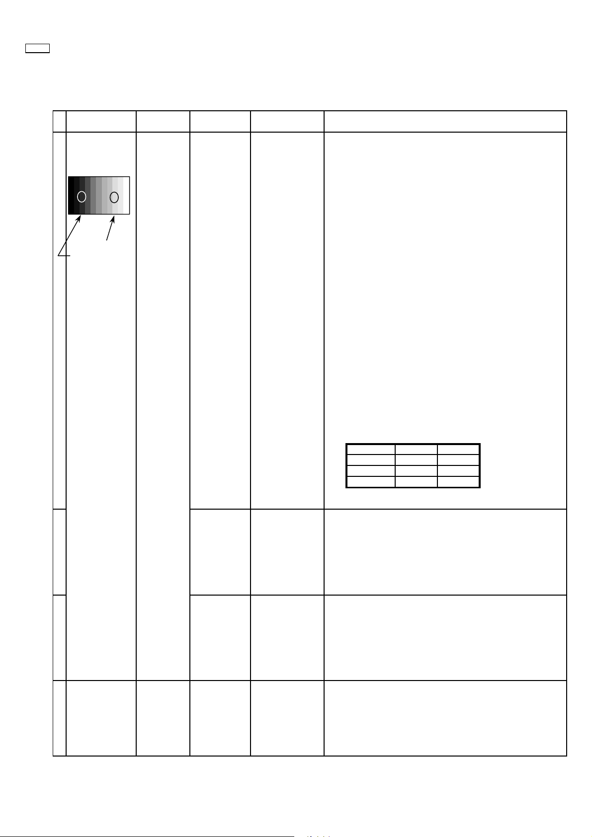
10 Alignment
10.1. 625i/625p panel white balance
INPUT Alignment menu ProcedureEquipment Setting
1 PC (625i) Color Picture: 1) Find the nearest area to brightness of 10 cd/m2 as Low
Gray Scale Analyzer Normal Sub Adjust light by color sensor.
Pattern White balance: Sub Bright 2) Adjust Sub bright to set Low light level to 10 cd/m
Cool
Aspect: PANEL W/B
16:9 G cut off 3) Set G cut off to " 80 ".
Component /RGB-in
Component shown Fig.-02.
High light 75% Sub Adjust
Low light 15% Sub Bright 5) If Sub Bright is changed re-adjust it to set Low light
PANEL W/B
PANEL W/B
PANEL W/B
exactly.
B cut off 4) Adjust B and R cut off to set color temperature as
R cut off
2
to 10 cd/m
6)Find 75% of white area by color sensor.
G Drive 7) Set G Drive to " E8 ".
B Drive 8) Adjust B and R Drive to set color temperature
R Drive as shown Fig.-02.
.
2
9) Repeat procedure 4) to 7) to set both Low light and
high light.
PANEL W/B
All Drive 10) Set All Drive to "FC".
PANEL W/B
R,G,B cut off 11) Re-adjust Low light level again.
Color Temp. x y
Cool(Hi) 0.276 0.276
Normal(Mid) 0.288 0.296
Warm(Low) 0.313 0.329
Fig. -02
2 Picture: 1) Change white balance to "Normal".
Normal PANEL W/B
White balance: R,G,B cut off 2) Repeat procedure 3) to 11) of Cool mode.
Normal
PANEL W/B
Aspect: R,G,B Drive
16:9
3 Picture: 1) Change white balance to "Warm".
Normal PANEL W/B
White balance: R,G,B cut off 2) Repeat procedure 3) to 11) of Cool mode.
Warm
PANEL W/B
Aspect: R,G,B Drive
16:9
4 Picture: Picture Menu 1) Change color templature to "Cool".
Normal Sub Adjust
White balance: Sub Bright 2)Re-set Sub bright to "30"
Cool
Aspect:
16:9
– 16 –
Page 18
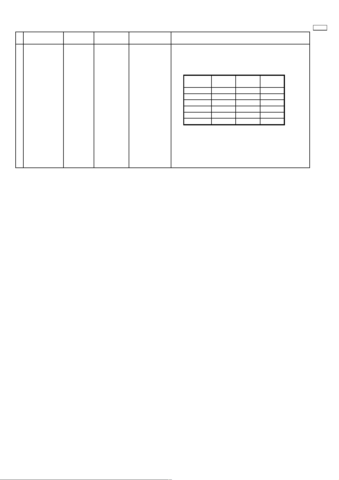
Alignment menu ProcedureEquipment Setting
5 Picture:PC (525i) 1) Write down each color temaparature of R,G,B drive and
Normal Cut off data as follows.
Aspect:
16:9
White
White balance:
Cool
Normal
Warm
Balance Cool Normal Warm
R Drive
G Drive
B Drive
R Cut off
G Cut off
B Cut off
2) Input 525i signal.
3) Copy 625i R,G,B drive and cut off data of each white
balance mode to 525i position.
50XP37
– 17 –
Page 19
50XP37
10.2. PC/RGB panel white balance
INPUT Alignment menu ProcedureEquipment Setting
1 PC (VGA) Color Picture: 1) Find the nearest area to brightness of 10 cd/m2 as Low
Gray Scale Analyzer Normal Sub Adjust light by color sensor.
Pattern White balance: Sub Bright 2) Adjust Sub bright to set Low light level to 10 cd/m
Aspect: PANEL W/B
Component /RGB-in
High light 75% Sub Adjust
Low light 15% Sub Bright 5) If Sub Bright is changed re-adjust it to set Low light
Cool
exactly.
16:9 G cut off 3) Set G cut off to " 80 ".
PANEL W/B
B cut off 4) Adjust B and R cut off to set color temperature as
RGB shown Fig.-03.
R cut off
to 10 cd/m
2.
6)Find 75% of white area by color sensor.
PANEL W/B
G Drive 7) Set G Drive to " E8 ".
PANEL W/B
B Drive 8) Adjust B and R Drive to set color temperature
R Drive as shown Fig.-03.
9) Repeat item 4) to 7) to set both Low light and
high light.
PANEL W/B
All Drive 10) Set All Drive to "FC".
2
PANEL W/B
R,G,B cut off 11) Re-adjust Low light level again.
Color Temp. x y
Cool(Hi) 0.276 0.276
Normal(Mid) 0.288 0.296
Warm(Low) 0.313 0.329
Fig. -03
2 Picture: 1) Change white balance to "Normal".
Normal PANEL W/B
White balance: R,G,B cut off 2) Repeat procedure 3) to 11) of Cool mode.
Normal
PANEL W/B
Aspect: R,G,B Drive
16:9
3 Picture: 1) Change white balance to "Warm".
Normal PANEL W/B
White balance: R,G,B cut off 2) Repeat procedure 3) to 11) of Cool mode.
Warm
PANEL W/B
Aspect: R,G,B Drive
16:9
4 Picture: Picture Menu 1) Change color templature to "Cool".
Normal Sub Adjust
White balance: Sub Bright 2)Re-set Sub bright to "30"
Cool
Aspect:
16:9
– 18 –
Page 20
10.3. HD panel white balance
INPUT Alignment menu ProcedureEquipment Setting
1PC(HD:720i or 1080i) Color Picture: 1) Find the nearest area to brightness of 10 cd/m2 as Low
Gray Scale Analyzer Normal Sub Adjust light by color sensor.
Pattern White balance: Sub Bright 2) Adjust Sub bright to set Low light level to 10 cd/m
Cool
Aspect: PANEL W/B
16:9 G cut off 3) Set G cut off to " 80 ".
PANEL W/B
Component /RGB-in
Component shown Fig.-04.
B cut off 4) Adjust B and R cut off to set color temperature as
R cut off
High light 75% Sub Adjust
Low light 15% Sub Bright 5) If Sub Bright is changed re-adjust it to set Low light
PANEL W/B
G Drive 7) Set G Drive to " E8 ".
PANEL W/B
R Drive as shown Fig.-04.
exactly.
2
to 10 cd/m
.
6)Find 75% of white area by color sensor.
B Drive 8) Adjust B and R Drive to set color temperature
50XP37
2
9) Repeat item 4) to 7) to set both Low light and
high light.
PANEL W/B
All Drive 10) Set All Drive to "FC".
PANEL W/B
R,G,B cut off 11) Re-adjust Low light level again.
Color Temp. x y
Cool(Hi) 0.276 0.276
Normal(Mid) 0.288 0.296
Warm(Low) 0.313 0.329
Fig. -04
2 Picture: 1) Change white balance to "Normal".
Normal PANEL W/B
White balance: R,G,B cut off 2) Repeat procedure 3) to 11) of Cool mode.
Normal
PANEL W/B
Aspect: R,G,B Drive
16:9
3 Picture: 1) Change white balance to "Warm".
Normal PANEL W/B
White balance: R,G,B cut off 2) Repeat procedure 3) to 11) of Cool mode.
Warm
PANEL W/B
Aspect: R,G,B Drive
16:9
4 Picture: Picture Menu 1) Change color templature to "Cool".
Normal Sub Adjust
White balance: Sub Bright 2)Re-set Sub bright to "30"
Cool
Aspect:
16:9
– 19 –
Page 21
50XP37
11 Trouble shooting guide
11.1. Self Check
1. Self-check is used to automatically check the bus line
controlled circuit of the Plasma display.
2. To get into the Self-check mode, press the volume down
button on the customer controls at the front of the set, at the
same time pressing the OFF-TIMER button on the remote
control, and the screen will show :-
If the CCU ports have been checked and found to be incorrect
Or not located then " - - " will appear in place of " OK "
11.2. No Power (Power shut down)
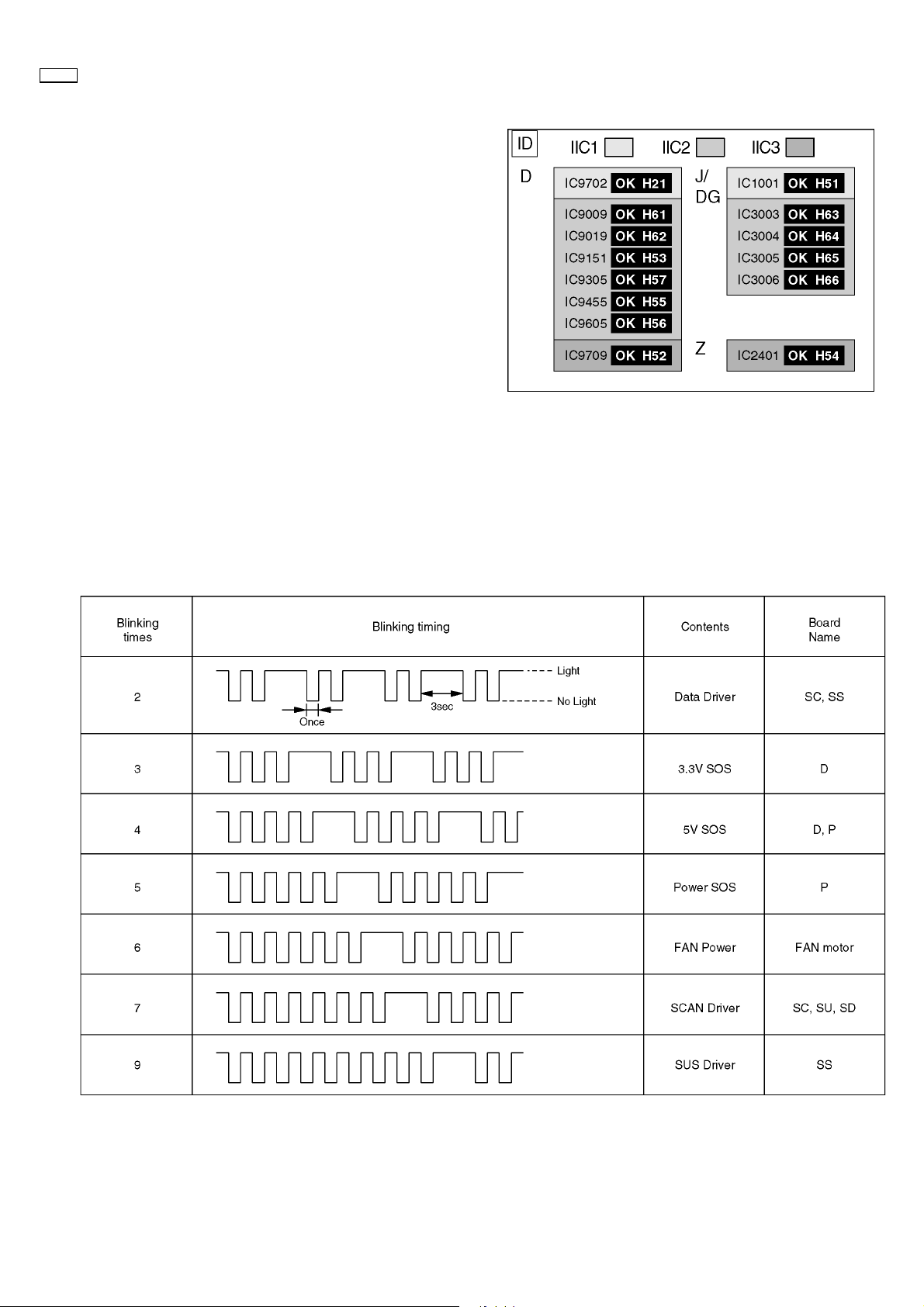
11.2.1. Power LED Blinking timing chart
1. Subject
Information of LED Flashing timing chart.
2. Contents
When an abnormality has occurred the unit, the protection circuit operates and reset to the stand by mode. At this time, the
defective block can be identified by the number of blinkes of the Power LED on the front panel of the unit.
– 20 –
Page 22

11.2.2. Power LED no light
11.3. No Picture
50XP37
– 21 –
Page 23

50XP37
11.4. Local screen failure
Plasma display may have local area failure on the screen. Fig - 1 is the possible defect P.C.B. for each local area.
Fig - 1
– 22 –
Page 24

12 Conductor Views
12.1. PF-Board
6
PF-BOARD(FOIL SIDE)
TXNPF10QMS
TP901
C925
D922
EBC
Q903
R927
1
PF10
6
TP903
R923
C924
R925
R926
R928
R924
R
A
K
IC902
D907
COLD
C917
R907
R905
TP902
R920
D923
R921
C918
JS901
JS905
TP904
R922
C920
D904
C915
S
LIVE
CIRCUIT
JS904
R906
D906
D920
C921
C922
V2
C916
C
HOT
T8AH250V
CAUTION
5
4
3
2
RL901
L904
D921
C923
S1 S2
T901
IC901
D
D901
D903
1
PF9
JS902
JS903
4
T3.15AL250V
CAUTION
PTP2V1
P1
R904
C919
L906
C914
T8AH250V
CAUTION
F900
F901
F902
R903
C912
C901
C910
C911
D902
JS907
JS908
C913
14
PF1
JS909
50XP37
C908
L903
C907
L902
PF
C905
C909
COLD
C906
C904
Parts Location
PF-BOARD (FOIL SIDE)
IC
IC901 B-3
IC902 A-3
TRANSISTOR
L901
Q903 A-5
TP
TP9001 A-5
TP902 A-5
TP903 A-4
TP904 A-4
JS906
L905
-
HOT
LIVE
CIRCUIT
+
C902
PF
R901
R902
PbF
C903
2
94V-0
SEE REVERSE FOR ORDER NO.
TNPA2891
1
PF-BOARD TXNPF10QMS PF-BOARD TXNPF10QMS
ABCDEFGH I
– 23 –
Page 25

50XP37
6
PF-BOARD(COMPONENT SIDE)
TXNPF10QMS
C910
C908
5
C907
TNPA2891
4
ORDER
C904
NO.
C906
2
PF
3
L901
C909
L902
C905
COLD
+
C902
L903
JS906
JS907
JS908
L905
D902
LIVE CIRCUIT
HOT
R902
R901
C901
JS909
14
PF9
JS902
JS903
C912
C911
T3.15AL250V
CAUTION
F902
R903
L904
D921
C923
J4
S2 S1
C921
C922
-
C919
P1 V2
PT P2 V1
C913
L906
J102
C914
R904
D903
D
J3
C
D920
C916
IC901
D906
JS904
R906
T901
J2
RL901
D922
C925
R927
Q903
R926
PF10
J1
1
6
R928
JS905
D923
PF
J103
J101
R923
R920
R921
R922
R924
C924
C920
S
D904
C915
C918
C917
ARK
IC902
D907
R907
R905
94V-0
R925
COLD
Parts Location
PF-BOARD (COMPONENT SIDE)
IC
IC901 B-3
IC902 A-3
TRANSISTOR
Q903 A-5
CAUTION
2
C903
14
PF1
T8AH250V
F900
F901
CAUTION
T8AH250V
D901
HOT
JS901
1
LIVE CIRCUIT
PF-BOARD TXNPF10QMS PF-BOARD TXNPF10QMS
ABCDEFGH I
– 24 –
Page 26

12.2. P-Board
6
5
50XP37
P-BOARD(FOIL SIDE)
TNPA2890
4
3
2
1
P-BOARD TNPA2890 P-BOARD TNPA2890
ABCDEFGH I
– 25 –
Page 27

50XP37
P-BOARD(COMPONENT SIDE)
TNPA2890
6
5
4
3
2
1
P-BOARD TNPA2890 P-BOARD TNPA2890
ABCDEFGH I
– 26 –
Page 28

50XP37
P
Parts Location
IC
IC401 H-3
IC402 H-3
IC403 H-3
IC404 H-3
IC406 F-2
IC408 G-3
IC409 G-3
IC501 H-5
IC502 H-5
IC503 H-4
IC504 H-4
IC511 F-5
IC512 F-6
IC520 G-4
IC521 B-3
IC522 B-3
IC523 G-4
TRANSISTOR
Q401 F-1
Q404 D-2
Q406 E-3
Q407 E-1
Q409 G-3
Q410 D-1
Q411 D-1
Q412 E-4
Q413 E-4
Q414 C-2
Q415 B-1
Q416 H-2
Q420 F-1
Q421 F-3
Q501 H-4
Q502 H-4
Q503 H-5
Q504 B-2
Q506 B-3
Q508 G-5
Q509 G-5
Q510 G-5
Q511 B-4
Q512 B-3
Q513 B-3
Q514 B-2
Q515 B-2
P-BOARD (FOIL SIDE)
Q516 C-3
Q517 B-3
Q518 F-4
Q519 F-4
Q520 B-3
Q521 H-4
Q522 H-5
Q524 G-4
Q525 B-2
Q527 F-5
Q528 B-3
Q530 F-5
Q531 F-5
Q532 G-5
Q535 H-5
Q537 G-5
Q540 G-4
Q541 G-4
Q542 F-5
Q544 G-5
Q545 F-4
Q546 G-6
Q547 H-4
Q549 G-4
Q550 H-6
Q551 H-5
Q552 H-5
Q553 G-6
Q554 G-6
TP
TP1 D-2
TP2 C-3
TP3 D-3
TP4 D-3
TP5 E-2
TP6 E-2
TP7 E-1
TP8 E-2
TP9 C-6
TP10 B-6
TP11 C-6
TP12 C-6
TP13 F-4
Parts Location
P-BOARD (COMPONENT SIDE)
IC
IC406 D-1
IC409 C-3
IC504 B-4
IC511 C-5
IC512 D-6
TRANSISTOR
Q406 E-2
Q410 G-1
Q412 E-4
Q413 E-4
Q414 G-2
Q415 H-2
Q527 D-6
Q531 C-5
P-BOARD PARTS LOCATION P-BOARD PARTS LOCATION
– 27 –
Page 29

50XP37
12.3. HX-Board
6
5
HX-BOARD(FOIL SIDE)
TZTNP01SCSH
HX
1
R668
R663
R538
L514
R654
C561
JK513
JK509
15
6
9
5
9
L515
D509
D507
R511
D510
R510
D508
TNPA2842
SEE REVERSE FOR ORDER NO.
CR NO.3
PbF
4
JK511
1
6
3
11
5
10
15
HX-BOARD(COMPONENT SIDE)
TZTNP01SCSH
ORDER
NO.
R400
R589
C523
R778
C524
R585
C564
E
B
5
D501
JK511
JK513
R776 R777
R653
R537
Q531
R655
R789
B
L516
C550
Q532
TNPA2842
PbF
A
R781
R784
Q533
Q535
R788
R783
Q534
C551
L517
D503
R672
R547
L512
R529
R530
1
6
JK509
HX
1
12
C405
C404
IC502
L555
1
C563
R782
Q536
L513
8
R590
4
5
R586
A
R664
R656
C562
R548
D502
CR NO.3
R787
R786
111
HX1
D
R780
R785
C409
22
R791
C566
C567
L526
D506
R790
C
L511
L507
L508
L509
L510
D504
R794
Q537
R591
R592
R593
R526R527R528
E
D505
R792
C565
D
R509
R508
C
1
HX
Parts Location
IC
IC3502 E-4 Q3531 D-4
HX-BOARD
TRANSISTOR
Q3532 D-4
Q3533 E-4
Q3534 E-4
Q3535 E-4
Q3536 E-4
Q3537 F-4
2
1
HX-BOARD TZTNP01SCSH HX-BOARD TZTNP01SCSH
ABCDEFGH I
– 28 –
Page 30

12.4. HV-Board
6
Parts Location
IC
IC3201 A-3
IC3251 B-4
HV-BOARD
TRANSISTOR
Q3002 B-2
Q3004 B-2
Q3006 B-2
Q3007 C-2
Q3051 B-2
Q3052 A-2
Q3101 B-2
Q3102 C-2
Q3104 B-2
Parts Location
IC
IC3001 G-2
IC3002 F-2
IC3003 G-2
IC3101 F-3
IC3102 G-2
IC3103 G-3
IC3104 F-2
IC3105 H-3
IC3301 H-3
IC3302 F-4
IC3303 H-3
IC3304 H-2
IC3305 H-2
IC3699 H-2
HV-BOARD
TRANSISTOR
Q3001 G-2
Q3003 F-2
Q3005 F-2
50XP37
5
RTB031
HV-BOARD(FOIL SIDE)
TXNHV10QWS
1
HV
PbF
1
C202
IC201
70
R314
Q052
JK005
56
R315
R313
R051
C053
L
TNPA2844
IC251
R188
C154
C152
C149
C134
C137
R302
R304
R193
R131
JS306
R319
C055
R057
R059
JS310
GRB
28
C171
C153
C151
C150
R192
R053
R053
ORDER
29
C170
C172
R151
R125
R141
R140
R104
R117
C006
Q051
Q051
R008
R009
NO.
C251
C169
C135
R013
R017
H1
C252
R163
R165
R164
C167
C168
R156
R172
R157
R152
C136
R118
R114
C121
R130
R136
R129
R108
R102
Q104
R012
R027
R063
R006
D002
R310
R312
R311
C162
R170
R171
R169
C178
C173
R177
R134
R135
C112
C119
C115
C001
R127
R128
R132
R119
R106
Q101
Q002
Q006
R043
C017
R032
R037
R003
R004
Q004
R030
R020
JK001
CY
A1
A2
4
CR No.3
94V-0
3
C206
35
36
C212
C212
C213
C213
2
SLOT
C214
C214
C211
C211
C209
R
R
R
C204
C205
C208
R307
R308
R309
C056
R056
R052
C054
12 3
C203
JK004
1
C210
R303
R055
R058
R054
R060
HB
A39
A40
B39
B40
R120
C177
C176
C174
C175
C181
R178
C180
R180
R153
R173
R179
C140
JS305
C120
R126
C109
R133
Q102
R115
R107
R101
R042
C015
L005
R026
R007
C016
C022
JK002
R044
JS304
R047
C021
R040
L007
Q007
R046
R045
R041
R050
R039
RTB031
HV-BOARD(COMPONENT SIDE)
TXNHV10QWS
A39
A40
IC002
B39
B40
H1
C311
R301
R300
CR No.3
R159
IC302
C308
R185
L106
1
IC101
R112
C020
C102
C019
C018
NP
NP
JS301
IC104
R038
L006
6
7
R028
Q023
C024
R001
TS302
5
C184
1
1
L105
R175
R176
R161
C165
C182
C159
C159
5
C127
Q003
R014
R014
C161
C144
C179
C142
C133
C160
C103
C132
C129
C105
R113
C128
C126
C125
R144
R145
64
64
R146
R142
R142
R143
R143
JS302
JS302
4
5
1
1
R036
12
R049
C007
R018
R021
NP
C004
C004
R064
R025
JK002
R031
R031
3
4
5
3
1
4
1
8
5
R023
R015
L003
C002
C005
R010
R011
R002
TS301
R182
Q001
R174
R166
256
1
65
65
IC001
R016
GBR
D302
R167
R160
C163
IC003
IC003
5
5
C008
1
1
R022
R022
L001
R024
TS303
D304
C330
L308
C325
R116
C187
D303
D301
R181
C166
C164
C164
R168
C110
C110
C113
C113
R121
R121
C111
C111
R029
R029
IC102
IC102
C114
C114
C104
C104
R122
R122
C108
C108
C023
C023
C107
C107
C014
C014
4
4
3
3
R019
C012
C012
C
JK001
C329
C321
L307
C261
C185
C186
R183
R184
R162
C183
C117
C117
C106
C116
C106
C116
R123
R123
R065
R065
C013
C013
C011
C011
C326
L004
C009
C003
NP
R005
L002
Y
JK005
SEE REVERSE FOR ORDERNO.
TNPA2844
1
HV
HB
94V-0
Q005
R035
C122
C010
R033
R034
R048
A1A2B1B2
C324
C320
R252
C264
R253
L251
C255
C255C264
C256
X101
193
192
192
IC103
129
128
C123
C118
89
R139
R138
R138
R124
R124
R137
R137
D001
D001
9
C301
JS303
R061
JS309
C322
C266
L252
C263
C260
C262
C259
C157
R251
C156
C155
C147
R158
R155
C158
C138
C146
C145
C139
C143
R154
C131
IC301
4
4
C130
R189
C216
C124
1
1
14
R195
IC105
5
R194
C188
1
IC305
5
5
8
8
C316
16
IC304
1
4
R062
L051
JS308
B
C051
L306
C328
C319
C265
C323
R255
R254
L104
L103
L103
C148
L102
C141
3
3
C218
C217
R208
2
2
L201
18
1
C207
R337
8
5
R338
1
4
C317
IC699
L052
L
L
C052
325
325
C215
C327
L305
C318
C253
C254
C258
C257
GND
TS100
VD
TS101
HD
TS102
R305
R305
L303
L303
C313
C313
IC303
1
1
C309
R149
R148
C219
H0
PbF
JK004
RGR
R
1
HV-BOARD TXNHV10QWSHV-BOARD TXNHV10QWS
ABCDEFGH I
– 29 –
Page 31

50XP37
12.5. HZ-Board
6
IC
IC3001 G-3
IC3002 H-3
Parts Location
HZ-BOARD
IC
IC3002 A-3
TRANSISTOR
Q3001 G-2
Q3002 H-2
HZ-BOARD
TP
TP032 F-4
TP033 G-4
TP034 G-4
TP035 G-4
TP036 G-4
5
Parts Location
RTB033
HZ-BOARD(FOIL SIDE)
TXNHZ10RCS
TNPA2952
A1
A2
4
1
IC002
8
PbF
4
5
B1
B2
CR NO.3
ORDER
NO.
H1
3
2
JK002
R
L
R
Pr
JK001
HZ
1
A39
A40
B39
B40
B
Pb
GR
Y
RTB033
HZ-BOARD(COMPONENT SIDE)
TXNHZ10RCS
CR NO.3
JS014
R043
PbF
JS001
C016
HZ
TNPA2952
SEE REVERSEFOR ORDERNO.
JS002
R008
R009
R046
C024
1
JS003
C002
C001
A40
TP032
Y
R038
C020
C019
R029
R020
C009
R001
Y
A39
B39
B40
C017
R021
C003
NP
JS011
L001
GR B
R039
JS015
R044
R034
R010R011
C025
R002
TP034
TP033
Pr
Pb
JS016
R035
C014
16
9
8
1
IC001
R047
C013
C005
C004
NP
JS012
R003
L002
R045
R031
Pb
R040
C015
R032
R030
TP035
RL
L007
JS013
JK001
C018
R033
R027 R028
NP
L003
TP036
R041
R012 R013
C026
C006
H1
C022
R042
JS004
JS005
R024
JS006
R048
R
Pr
JS009
C023
JS010
L006
C011
C012
R025
R022
C010
Q001
R016
R018
R017
C008
R007
L004
R004
JK002
LR
A1
A2
B1
B2
JS007
JS008
IC002
58
R037
D003D004
R023
R026
Q002
R014
R019
R015
C007
R006
L005
R005
14
C021
R036
D001
D002
H0
1
8
SLOT
1 2 3
1
HZ-BOARD TXNHZ10RCSHZ-BOARD TXNHZ10RCS
ABCDEFGH I
– 30 –
Page 32

12.6. HT-Board
50XP37
Parts Location
6
IC
IC4601 B-4 Q3441 C-2
HT-BOARD
TRANSISTOR
Q3442 C-2
Q3501 B-2
Q3502 A-2
Q3503 B-2
Q3504 B-3
Q3505 A-3
Q3506 B-3
Parts Location
IC
IC3301 H-3
IC3305 G-4
IC3311 F-3
IC3441 F-2
IC3501 G-2
IC3699 F-4
IC3701 F-3
IC3702 G-3
HT-BOARD
TRANSISTOR
Q3401 G-2
Q3402 G-2
Q3461 H-2
Q3701 F-2
5
RTB032
HT-BOARD(FOIL SIDE)
TXNHT10QYS
TNPA2847
HT
ORDER
NO.
A1
4
3
JS306
94V-0
2
A2
B1
B2
H1
56
1
R413
R530
R544
R529
Q505
C512
R535
R538
TS502
R
R526
TS503
G
R532
R527
Q502
R524
R523
R548
C508
R520
R512
R515
R509
R511
R508
C516
R547
29
IC4601
28
R730
R731
JS315
JS316
R545
C303
Q506
R539
R533
R521
R518
R507
C515
Q504
C510C511
R536
R540R541 R542
TS501
R528
B
R531
R525
Q503
R522
C509
R505
R510
R506
R549
1
R312
R534
R537
R543
Q501
C507
R519
JS307
C513
R504
C517
JS312
R403
C406
1
1
1 23
2
R323
JK102
JS305
C720
C408
PbF
R311
CR NO.3
A39
A40
B39
B40
R308
R310
R309
JS313
C718
C725
C726
C727
R716
R318
JS311
C721
Q441
R404
R442
R446
R443
R314
R325
R324
R316
R315
JS304
C716
C715
C714
C717
C710
R715
R712
L702
C445
R449
R448
R445
R447
R444
C321
Q442
21
20
RTB032
HT-BOARD(COMPONENT SIDE)
TXNHT10QYS
A39A40
B39
D502
D501
IC699
PbF
JS302
C708
C703
C709
HT
TNPA2847
SEE REVERSE FOR ORDER
NO.
1
B40
D503
D504
8
C324
1
1
4
C705
R707
R727
R710
R709
C704
L701
X701
NP
R704
R705
C322
C443
C323
5
JS314
C312
4
8
5
IC311
R327
R326
41
IC701
C706
C702
R706
R708
64
R713
C707
C713
C701
R703
Q701
R452
R453
3
R450
IC441
L442
21
20
TS302
VD
R319
IC305
16
C315
1
R317
L305
C314
40
65
C711
R711
5
R717
C723
C719
C728
C733
R714
C712
L703
NP
C410
R701
R412
R451
R702
C444
4
R408
C412
Q402
R441
C442
L441
HD
TS301
R321
R320
R313
C320
C318
C319
9
8
R718
C724
C731
25
24
1
C742
R721
80
C722
JS310
C409
R402
NP
C411
R410
R406
L404
R405
R407
JS308
C441
C317
R322
R719
C732
IC702
3
4
R725
C738
C739
C740
C730
C729
R401
R411
R409
C402C404
R305
R306
R307
1
C743
6
7
C514
Q401
L402
R720
R729
R722
C741
R723
R724
C734
C746
L301
5
R728
C744
C745
C309
LC501
R550
R551
NP NP
C504
R501
JS309
C302
R4604
R546
A1A2
B1
B2
H1
C4603
C4604
R4607
R4612
C4602
C4608
C4607
R4605
C4605
C4606
C4609
C4610
C4611
C4612
R4608
R414
JS301
1
12
9
16
C501
R303
R4557
C325
1
C326
C301
R302
C311
L302
C304
L303
C306
6
7
R516
R502
R304
1
JK102
2
LC503
1
R513
8
IC501
1
R517
R514
C502 C503
C505
R461
C461
C307
6
12
7
Q461
R462
C4618
R4611
C4617
C4616
L4603
CR NO.3
L4602
L4601
C4615
C4614
C4613
IC301
5
R301
L304
JS303
C316
LC502
NP
C506
R503
R466
R465
R463
R464
C313
C305
C308
C310
94V-0
1
12
H0
1
8
HT-BOARD TXNHT10QYSHT-BOARD TXNHT10QYS
ABCDEFGH I
– 31 –
Page 33

50XP37
12.7. J-Board
6
5
J
Parts Location
J-BOARD (FOIL SIDE)
IC
IC8003 I-2
IC8004 F-2
TRANSISTOR
Q3001 G-3
Q3002 D-2
Q3003 D-2
Q3101 H-2
Q3102 H-2
Q3103 H-1
Q3104 H-2
Q3105 H-2
Q3106 H-2
Q8001 G-2
Q8002 I-2
4
J-BOARD (FOIL SIDE)
TNPA2826
R3025
C8070
C8072
JS8091
B40
B39
A40
A39
D3012
D3010
D3014
D3015
D3013
R3046
C8073
R3230
B40
B39
A40
A39
3
2
ZA3008
ZA3007
R3059
D3004
J13
B2
B1
A2
A1
ZA3005
C3005
Q3002
Q3003
R3011
R3013
R3009
R3010
R3012
R3014
C1004
C3006
R3022
R3160
R3161
JS8090
R1003
R3145
R3146
C3002
C3003
R3005
R3006
R3007
R3008
PbF
J14
12 22
C3205
111
TNPA2826 1 J
SEE REVERSE FOR ORDER NO.
123
ZA3006
D3011
R3035
R3044
R3100
R3099
R3047
R3045
R3034
R3197
R3036
R3084
R3085
R3041
J12
R3040
R3029
R3195
R3039
R3196
R3198
R3028
R8057
R8044
R8046
R8058
R8049
R8051
R8059
C8037
R8042
C8026
R8034
C8024
C8020
IC8004
R8032
R8068
C3105
R3188 R3189
R3190
R3260
R3261
R3262
R8054
R8043
R8045
R8055
R8048
R8050
R8056
C8036
R8041
C8025
R8033
R8011
R8018
J11
R8012
IC8003
C8023
C8019
R8017
R8010
R8009
R8031
B2
B1
A2
A1
R8001
R8004
ZA3001
R8002
R8003
D8003
R8025
R8026
D8001
1
20
11
C8013
R8067
R8065
R8066
R8072
C8061
R8093
10
C8060
R8081
R8077
R8079
R8029
Q8002
R8036
R8035
C8027
C8064
C8021
C8065
JS8092
C8028
ZA3002
B2
A2
1
20
11
C8014
R8070
R8082
R8078
R8080
R8069
R951
B1
D3001
A1
R8027
D8004
C8042
10
R8030
ZA3004
R8060
R8028
JS8093
C8041
C8022
D8002
R8098
R8100
R8061
Q8001
C8062
C8043
C8063
R8097
R8099
R8063R8064
R8062
R8091
C3016
C3014
R3056
R3002
R3001
R3058
R3049
ZA3003
R3055
R3057
Q3001
R3052
C3013
R3048
C3017
R3051
R3003
R3063
C3012
C3015
Q3105
Q3104
Q3101
R3132
R3130
R3128
Q3102
R3131
Q3103
C3253
R3199
R3202
R3129
R3133
B40
B39
A40
A39
C3252
C3251
R3251
R3297
R3103
R3106
C3255
R3117
C3108
R3203
R3254
R3257
C3261
R3111
C3114
R3255
JS8096
R3118
R3114
R3299
R3252
R3110
R3109
C3104
R3298
R3253
R3107
R3108
R3112
R3102
Q3106
R3105
R3101
R3104
R3204
R3201
C3106
C3113
C3260
R3200
R3256
R3113
1
J-BOARD TNPA2826 J-BOARD TNPA2826
ABCDEFGH I
– 32 –
Page 34

50XP37
J
Parts Location
J-BOARD (COMPONENT SIDE)
IC
6
5
4
J-BOARD(COMPONENT SIDE)
IC1001 F-2
IC3001 F-2
IC3002 D-2
IC3003 D-2
IC3004 D-3
IC3005 C-2
IC3006 D-2
IC3007 E-1
IC3108 B-2
IC3109 B-1
IC3201 B-2
IC3251 B-2
IC8001 A-3
IC8002 D-3
IC8003 A-2
IC8004 D-2
IC8005 A-2
IC8006 D-2
IC8007 A-1
IC8008 C-2
IC8009 C-2
IC8015 H-1
IC8016 E-2
IC8020 A-2
IC8021 D-2
IC951 F-3
IC952 F-3
TRANSISTOR
Q3010 E-3
Q3011 E-3
Q8010 E-2
Q8011 E-2
Q8012 E-2
Q8013 E-2
TP
TPJH1 A-2
TPJH2 D-2
TPJV1 A-2
TPJV2 D-2
TNPA2826
R3067
R3090
R3078
C3028
C3018
R3073
R3068
R3074
R3089
R952
C3027
L3006
R3069
R3075
R3077
C3026
R3088
R3076
R8071
R8094
5
C8051
C960
C8044
1
J3
2
L954
C954
4
1
IC8008
C8066
8
C8050
5
8
JS8099
1
4
IC8021
IC8009
R8087
C8048
R8085
R8024
C8006
R8006
NP
C8012
C8018
R8005
D8006
D8008
ZA3004
R8022
IC8002
R8007
JS8095
R8008
C8008
C8011
C8017
D3023
B2
1
B1
A2
A1
C8002
C8004
16
1
8
9
R8020
R8019
R8096
IC8004
20
1
R8040
C8034
C8067
1110
1
TPJV2
TPJH2
7
IC8006
L8002
14
8
L8006
R8014
R8015
R8016
C8031
C8039
R8013
R8038
21
IC3004
L8004
C8032
L8007
C8046
R3083
IC3003
IC3002
R3033
J6
1
R3082
1
R3170
R3026
R3032
R3027
16
89
R3030
R3031
1
16
8
16
9
8
16
1
8
9
IC3006
R3172
J12
B40
B39
A40
A39
D3003
C956
C3011
Q3010
R3042
R3153
R3152
R3151
C3009
R3094
R3095
R3096
R3097
R3098
C3010
C3032
L3005
R3087
L3003
Q3011
R3037
R3038
R3150
R3219
Q8012
Q8013
R3214
R3215
D8011
R3231
C3040
1
8
45
IC3007
R3140
R3141
C3041
R3233
14
R3235
R3024
Q8011
R3023
R3218
R3211
8
7
1
IC8016
L3050
C3200
R3043
9
R3086
D8010
R3234
R3216R3217
C8071
2
20
J8
1
19
C964
C958
L957
L958
L959
ZA3005
C963
C957
C962
R3018
89
R1001
R1002
IC3001
R3021
Q8010
R3213
R3212
R3210
R3232
R3017
C1004
R3020
R3016
C955
IC952
R3015
1
16
R3019
B2
B1
A2
A1
C968
L955
L956
L960
C961
L1001
L3002
C3008
IC1001
D1001
C967
C3004
4
1
8
5
C1003
ZA3006
C970
C969
C3007
C1002
PbF
C965
C971
C972
IC951
C966
L3001
C3001
X9350
C1001
TNPA2826
ORDER
NO.
J13
1
J
16
9
16
L952
J10
C3203
22
L951
C952
C951
J14
111
R3060
ZA3008
R3061
12
B40
B39
A40
A39
ZA3007
IC8015
C3202
1
C3201
C3204
8
32
C3021
C3020
C959
R3080
R3091
C3022
39
L953
40
C953
ZA3003
R3079
C3029
C3030
C3031
R3054
20
19
R3053
R3050
C3019
1
64
C3025
C3024
C3023
R3064
R3070
R3065
R3071
R3066
R3072
131
J5
J11
B2
B1
A2
A1
3
C8016
2
JS8098
TPJV1
R8084
C8047
R8083
ZA3002
L8001
C8001
C8033
C3266C3267
16
C8003
9
C8030
C3268
C8029
R8039
C8038
C3135
L8005
14
R8037
C8045
C3136
IC8005
8
C8040
NP
C8049
8
C3134
R8089
5
C3257
C3258
R3127
R8088
IC3251
C3111
14
15
C3110
14
15
R3124
R3123
R8090
R3120
R3122
C3116
C3112
C3117
R3115
C3254
C3256
8
21
22
C3263
C3262
R3126
R3125
C3109
8
21
22
R3121
R3116
R3142
ZA3001
R8021
C8010
D8005
D8007
IC8020
1
IC8001
8
R8095 R3081
C8005
C8007
R8023
L8003
IC8003
20
1
C8009
C8015
JS8094
D3022
11
10
1
TPJH1
7
R8052
R8047
C8035
R8053
1
4
IC8007
B40
B39
A40
A39
R3004
R3143
R3191
C3144
R3192
C3259
C3264
R3258
C3115
C3143
IC3201
C3141
R3194
C3142
R3193
JS8097
D3024
33
C3265
IC3109
R3093
51
D3021
IC3108
R3092
IC3005
52
7
1
28
R3259
C3107
7
1
28
C3118
1
J-BOARD TNPA2826 J-BOARD TNPA2826
ABCDEFGH I
– 33 –
Page 35

50XP37
12.8. D-Board
D-BOARD(FOIL SIDE)
TZTNP02SCSH/TZTNP01SCSC
R974
R615
R629
R579
R427
R994
R983
11
20
C603
C601
20
11
20
R600
R624
Q602
R621
R377
R174
R442
R378
R379
C204
C201
1
R241
20
1
R218
R217
C191
C192
R231
R233
C199
C085
R018
R084
IC004
5
4
8
1
56
28
28
C042
29
IC013
5
4
1
8
56
R062
IC018
29
C056
IC007
C033
C038
R673
10
11
R602
1
IC603
10
1
IC604
Q601
R441
R227
C001
R603
10
R617
1
R604
R744
R979
R828
C602
R830
R620
C613
R177
R179
R618
R443
C164
C166
60
R083
R048
R030
C002
R049
5
1
R154
C167
C178
C165
C168
C173
C170
R205
R229
C203
C195
C177
R220
R221
R240
C202
R243
C627
C638
41
R975
R668
R667
R665
R664
R663
C636
R659
R661
R660
R126
R125
D001
R124
4
5
C005
3
1
C003
IC001
C037
R115
C114
R114
4
3
3
1
4
5
R584
R599
R598
R655
R585
R622
R623
R689
R690
R610
R611
IC601
R609
R614
R582
R583
R619
R608
C187
C176
C172
R234
R204
R230
40
61
R656
R831
C028
C029
C120
C004
C006
L001
C086
C087
C031
R612
IC703
R236
1
IC705
R573
R575
23
C733
R576
R574
1
IC602
20
C604
10
R790
1
C728
R784
R783
R168
C163
R169
R167
C159
4
R246
R247
5
R152
R111
R155
R151
R118
20
C640
R691
R666
1
R692
80
R658
R662
R002
C015
C019
C026
C017
3
C013
L003
R032
C075
C073
C067
R117
C061
5
3
1
1
3
4
5
R674
R678
R698
R613
R676
R581
R580
R677
10
11
11
20
R157
C731
R153
R202
C180
C179
C641
IC608
21
R657
R989
C637
C014
C018
C016
IC003
C023
4
C024
C022
5
C012
L002
C011
C121
C071
C070
C074
C072
C080
IC012
C081
3
4
1
5
C123
C076
C094
5
4
1
C097
R797
22
IC704
1
C727
R789
Q707
R718
C162
C158
C157
R180
3
C161
IC152
1
C160
D953
R959
C156
C154
C961
R669
R693
R723
R721
R719
R700
R716
R714
R711
R003
C021
R015
C020
R013
R016
R066
R067
10
11
R033
C079
R044
R041
C078
C083
R046
C124
C068
L008
D003
C062
C057
L009
C069
4
C059
C098
C101
3
IC010
R793
C734
R800
R801
R802
C730
C729
C715
C714
D729
R791
R806
Q701
R736
R761
R725
R960
R964
R712
R710
20
C100
IC017
R737
R961
C960
R709
R724
R722
R720
R717
R715
R713
R065
1
IC023
C077
D952R372
R962
+
IC951
C955
L952
R958
R952
L954
R951
L953
C954
L951
R133
R948
R699
R134
R135
R697
R694
C060
R730
R729
R728
L010
R727
R726
C125
C089
C091
R798
1
R764
C706
D715
D718
14
IC702
8
5
44
C724
C719
C726
R799
2140
20
C711
R758
R746
C716
C717
C766
R734
R735
15
C957
C972
R587
R588
R589
R957
R956
R955
R954
R953
D708
R696
R695
R132
R731
R590
D706
D707
D709
D712
IC711
D711
R116
C115
R130
R929
D722
R985
R928
D704
D705
R708
R707
Q703
R739
D710
D713
R733
R131
Q704
R738
4
1
C700
8
R949
5
Q719
D802
R805
R804
R803
D721
C185
IC014
C148
R105
R104
C048
R317
C599
R548
R425
R595
R981
R426
R973
R632
C626
R634
R565
R566
R567
R568
R643
R428
R982
R569
R679
R640
R641
R650
R653
R651
R652
R649
R945
IC706
11
R946
4
5
3
1
R814
IC606
10
R108
R136
R137
R184
C153
R183
R166
10
R123
IC154
11
C193
1
7
8
R228
IC157
14
8
C198
10
1
20
11
R064
R508
R507
R394
R395
R401
R396
R470
R402
C027
1
R385
R384
R054
R309
IC008
C050
C052
R050
C084
C092
R051
1
C112
R061
C108
C109
C111
C058
R120
C107
C110
C093
C034
C039
R110
C054
C030
R029
IC006
C032
C051
R019
R020
R023
R024
R113
R022
C053
C049
C035
C040
C036
C043
R344
Q709
R823
C741
R406
IC156
C339
C341
L309
C336
C335
C147
R060 C088
C146
R107
R106
C106
Q592
R596
Q598
R597
R345
R342
R354
R338
C639
R881
C769
R571
20
C737
R848
R572
1
R578
C744
R841
R577
R197
R198
4
5
C189
C330
R400
R399
C323
R383
R387
R388
C346
C325
C327
R119
C096
IC016
C090
R053
R055
R056
R052
C149
R028
R555
6
R592
C598
Q596
R594
R593
Q597
R552
R380
R556
R909
R910
R911
R908
R906
R907
5
CR NO.9
12
3
R419
R601
R418
4
PbF
C492
C491
C487
C490
3
SEE REVERSE FOR ORDER NO.
1TNPA2824
2
C479
D
C495
R553
C496
R547
C476
C489
R485
C475
R484
C485
R487
C473
R541
R538
R544
R535
R537
R532
R560
R562
R557
R558
R554
R905
R917
R862
C755
R497
C480
C484
R517
C758
D727
R897R898
C757
R904
R900
R903
R866
D719
R930
C767
R302
R942
R993
R991
R990
R992
R494
C452
R495
C451
R496
R498
R499
X451
C454
C486
C488
L452
C481
C478
C477
R488
R489
C470
R477
C483
C482
R486
C597
R376
R564
Q594
R515
R563
Q591
R307
R913
R919
4
R915
C760
5
C759
R918
R834
R835
R852
R853
R914
R901
R923
D723
C743
R879
R809
R829
C754
R819
D771
D714
Q717
R467
X452
R452
11
R451
20
C453
R449
C455
R490
R491
R479
R447
R478
R482
R483
R475
R476
C474
Q599
R510
C318
R305
C301
R310
R311
1
4
1
IC710
8
5
8
C748
D720
Q715
Q716
R941
R939
R940
R937
R935
R330
1
IC451
C463
IC707
IC708
5
C740
1
C750
R921
C763
R821
D769
R871
R347
R364
Q714
R934
C768
R933
R932
R931
R936
R340
R339
R322
10
R329
R456
R454
R453
R382
C345
C334
C340
C332
C315
Q593
R361
R360
Q301
R315
4
R826
R815
3
C745
R820
R870
R825
R827
R885
D730
C756
R925
C739
R822
R770
R884
R836
R838
R356
C746
R824
R842
R352
R355
R849
R850
C747
R839
R840
R348
R460
R362
R373
R381
R404
R403
R405
C343
C324
C329
C333
C342
C331
R392
C328
R391
C337
C338
R398
R397
C326
C316
R514
R513
C596
R586
R431
1
D-BOARD TZTNP02SCSH/TZTNP01SCSC D-BOARD TZTNP02SCSH/TZTNP01SCSC
ABCDEFGH I
– 34 –
Page 36

D-BOARD(COMPONENT SIDE)
TZTNP02SCSH/TZTNP01SCSC
50XP37
D27
9
D20
1
C951
39
12
C720
R769
C701
1
4
1
R773
R771
R774
L955
D25
D10
D3
R986
R984
1
R796
C723
R792
R777
C718
R775
R782
R776
R743
C710
C964
C952
8
1
C702
R779
R172
C155
R216
C962
R199
R226
R225
R212
R213
C971
R963
R998
C968
C953
C956
D954
121
D6
R005
R007
R008
R009
R011
C025
R014
C122
R035
1
R037
R038
D5
R039
C064
R042
R045
C082
31
C065
C066
C063
C102
C105
R684
R685
R675
X701
1
IC701
R170
R778
R781
R173
R190
R967
R211
16
Thermal pad
IC952
1
C010
IC011
C095
C103
C611
R109
R607
R686
R687
R688
C722
R785
160
R786
C607
R788
C609
D717
C725
R682
R787
121
C732
120
C708
R780
R171
23
22
21
20
19
R176
18
17
16
15
14
13
12
R760
11
10
9
8
7
6
5
4
3
2
R215
1
R214
A
R966
1
C970
1
BC
9
C966
8
C967
D955
C969
IC002
56
29
28
29
28
20
21
40
41
R616
208
1
C605
C606
C608
C610
52
R681
C612
R891
R867
R316
R248
R242
R112
D
FGHJKLMNPRTUVW
E
R969
R970
L956
R004
R010
R012
R017
56
R031
R036
R034
R040
R047
C113
C615
C614
53
C616
R178
R182
IC151
R968
C965
R965
R808
R947
R001
R006
28
C009
R043
IC019
1
80
60
C099
5
6
X703
R740
C772
R950
C771
R795
C774
C775
IC712
8
D728
C773
40
R772
R766
41
9
R755
C713
C712
5
4
CR NO.
R756
Q710
D
1
80
81
R762
R768
R888
R747
R765
R763
R767
R754
C765
R794
Q702
Q706
C707
R750
D716
R751
R753
R757
R759
C705
C958
R742
R741
R748
R745
R749
C959
TNPA2824
D22
ORDER NO.
11
L701
L601
12
R997
20
2
R705
R706
R701
C703
R732
R995
R996
D12
R988
R987
2
1
19
R704
R703
R702
40
1
3
2
C647
C646
R591
D4
1
C709
7
1
C622
C620
C618
C617
X151
R630
R201
R187
R245
R181
C181
86
R807
1
R972
IC005
1
1
21
61
40
R192
AAABAC
Y
C205
C182
Q001
R025
56
29
C007
56
C008
R057
Q002
IC015
29
C055
28
41
IC009
20
A40
C623
R638
157
C629
156
B40
R319
IC605
C630
R321
C631
1
105
104
4
R863
R813
C628
R639
R872
R811
C152
C151
C194
R244
C621
C619
1
C169
C171
C045
R465
C197
R063
R191
C190
IC155
43
D34
B1
C041
A1
R239
TP_HDS
C322
R374
TP0768
TP_VDS
R468
TP0767
5
23
21
19
17
15
11
7
5
3
1
PbF
R320
R605
R606
R627
R680
R683
R193
R194
R195
C206
R466
R219
R196
R232
R224
D150
R203
R165
R164
44
C200
R027
R026
C047
R129
R128
R127
C104
R058
R059
1
80
61
C046
C044
60
R351
R324
D31
R359
R332
8
5
IC607
R812
R810
D724
R647
R980
C624
C625
C175
L155
C174
C742
25
C344
IC153
48
C347
C183
C196
R222
R223
22
20
18
16
14
13
12
10
9
8
6
4
2
R375
C320
R318
R421
R446
R210
C186
R435
R407
CDE
A
G
F
B
30
R436
31
R439
R386
50
51
R323
R349
R357
R327
R363
R358
R369
R837
C313
IC306
R390
R389
C184
C188
R200
R409
IC305
R408
KLMNPRTUVWY
J
H
IC304
R365
R368
A1
L461
R314
B1
R122
R304
X702
C632
C633
C634
C635
R648
R644
R646
R645
R642
R393
C462
R437
R438
R353
R312
R346
R301
R350
R121
C317
Q708
C761
R920
R922
IC709
32
R637
R977
33
R976
R978
48
R654
49
C312
16
1
X302
R326
X453
C319
B40
A40
C314
8
9
R461
R371
24
R370
R366
R367
IC303
R336
R343
IC301
C306
1
1
C304
4
5
C459
R464
C321
1
10
L463
4
AB
AA
AC
C457
R459
1
R469
R505
R450
100
C456
R455
81
80
IC458
20
11
R331
R333
R334
R509
R511
R504
C308
C311
C309
8
1
TP_HDM
C448
R542
R545
C762
R472
C460
R457
R458
C461
C458
TP0889
TP0887
TP_VDM
C465
R303
R539
R536
R512
A40
C499
B40
R534
1
10
R926
C764
17
R533
R924
R896
16
R890
R887
R883
R880
R877
R876
R874
R869
R865
1
R861
R859
R857
64
C753
R855
C302
1
3
4
5
C307
R492
C494
C493
C310
48
R462
R493
8
C464
R528
R531
5
IC452
23
22
21
20
19
R463
18
17
16
15
14
13
12
11
10
9
8
7
6
5
4
3
2
1
A
R433
C472
C471
R971
IC453
5
1
R481
R520
R480
C466
R518
R335
R306
R337
R308
R328
R341
D33
R516
A1
20
11
R894
25
BCDE
R444
B1
IC457
R927
IC302
C305
31
50
R519
R892
C803
C804
C749
F
30
51
R525
R522
R527
R523
R521
C805
R912
C802
R938
D801
C303
R416
R833
R943
R817
R503
R502
R501
R500
KLMNPRTUVWY
GHJ
R526
R414
R851
R816
R530
D32
R524
16
L800
R410
R818
R445
R432
IC455
IC454
R543
R529
R550
9
1
8
R854
24
1
IC456
C752
C751
R440
R473
R474
R434
R551
R540
IC800
A1
B1
R325
R561
L460
R895
C498
R893
C497
R889
R916
R886
R549
R944
R882
R832
R878
R847
R875
R846
R845
R873
R902
C806
R899
R844
R843
R868
R864
R860
R858
C800
R856
C801
R413
C400
D800
R417
R420
Q400
C450
C449
AB AC
100
R635
R546
R415
56
29
R423
R422
C469
C468
C467
81
R625
R626
R631
R670
R671
R672
R636
L459
R313
L462
B40
A40
1
IC459
R411
28
AA
1
80
R628
R633
R506
R559
1
D-BOARD TZTNP02SCSH/TZTNP01SCSC D-BOARD TZTNP02SCSH/TZTNP01SCSC
ABCDEFGHI
– 35 –
Page 37

50XP37
D
Parts Location
IC
IC001 D-2
IC003 E-2
IC004 D-3
IC006 D-1
IC007 D-1
IC008 D-3
IC010 E-1
IC012 E-2
IC013 D-2
IC014 C-3
IC016 C-2
IC017 E-1
IC018 D-2
IC023 E-2
IC152 E-4
IC154 C-4
IC156 C-4
IC157 C-4
IC451 B-4
IC601 D-6
IC602 E-5
D-BOARD (FOIL SIDE)
IC603 D-6
IC604 D-5
IC606 D-5
IC608 E-3
IC702 F-6
IC703 E-5
IC704 E-5
IC705 E-6
IC706 C-5
IC707 C-6
IC708 B-6
IC710 B-6
IC711 F-2
IC951 F-4
TRANSISTOR
Q301 C-6
Q591 B-1
Q592 C-1
Q593 C-1
Q594 B-1
Q596 A-6
Q597 A-6
Q598 C-6
Q599 C-6
Q601 D-5
Q602 D-5
Q701 F-4
Q703 F-3
Q704 F-2
Q707 E-5
Q709 C-5
Q714 B-4
Q715 B-4
Q716 B-4
Q717 B-4
Q719 F-2
Parts Location
IC
IC002 B-3
IC005 C-3
IC009 C-2
IC011 B-2
IC015 C-2
IC019 C-2
IC151 C-4
IC153 D-4
IC155 C-3
IC301 E-4
IC302 E-4
IC303 E-4
IC304 D-2
IC305 D-4
IC306 D-4
IC452 E-4
IC453 E-2
IC454 F-2
IC455 F-3
IC456 F-4
IC457 E-6
D-BOARD (COMPONENT SIDE)
IC458 E-2
IC459 F-4
IC605 C-6
IC607 D-5
IC701 B-6
IC709 E-5
IC712 A-6
IC800 F-5
IC952 B-3
TRANSISTOR
Q001 C-3
Q002 C-2
Q400 F-5
Q702 A-4
Q706 A-4
Q708 D-6
Q710 A-5
TP
TP0767 D-3
TP0768 D-3
TP0887 E-3
TP0889 E-3
D-BOARD PARTS LOCATION D-BOARD PARTS LOCATION
– 36 –
Page 38

12.9. C1-Board
6
5
50XP37
C1
C1-BOARD(FOIL SIDE)
TNPA2903
4
123
2
C1TNPA2903
SEE REVERSE FOR ORDER NO.
CRNO.7
3
C1-BOARD(COMPONENT SIDE)
TNPA2903
CA1
L101 L102
2
55
R101
R105
C112
R117
R107
R106
R115
1
C102
R114
R118
C142 C143C144 C145C146 C147
C109
CRNO.7
L103 L104
R110
R111 R112
C104 C105C106
C141
D101
D102
C107
6
C1MM1
55
R102
C111
R116
R104
R103
1
C12
TNPA2903
ORDER
CA2
R113
1
C101
R109
R108
C103
D104
C110
PbF
D103
C108
2
C1
5
R135 R136
C127
C128
NO.
18
C13
55
C124
C123
1
R119
C113
IC101
R120
R163
R164
IC106
11
R175
R174
10
20
1
C134
R133
R123
R161
R160
R173
R159
R158
R172
CA3
L106 L107
1
C125
C121
IC105
10
11
20
1
C137C138
L108
R125 R126
R127 R128R129
C119
D108
D107
C117C118
R157
R156
R155
R154
IC104
11
R170
20
R169
L105
R153
10
R152
R151
R150
C132C133
C136
R130R131
R132
C122
C115
C148
D105
R168
R167
1
CA4
20
55
C126
R121
R141
C120
D106
C116
R140
R144
R179
R183
R139
R178
R182
R137
R181
R177
R138
R180
R176
R143
IC103
11
201
R122
R149
10
R148
R147
R146
1
C131
C135
R134
C114
R124
IC102
R184
R165
R166
R145
11
10
1
20
C129
C130
C11
1
R171
1
R186
R187
A40
B40
R185
DL101
C139
C140
R142
R162
B1
A1
C10
C1-BOARD TNPA2903 C1-BOARD TNPA2903
ABCDEFGH I
– 37 –
Page 39

50XP37
12.10. C2-Board
6
5
C2
C2-BOARD(FOIL SIDE)
TNPA2904
4
TNPA2904
SEEREVERSE FOR ORDERNO.
2
C2
31
2
3
C2-BOARD(COMPONENT SIDE)
TNPA2904
C22
L202
1
2
A1
A40
1
R226
C213
R241
R225
B1
20
C201
B1
A1
C20
B40
C232
C210
55
R227
D201
C203
R211
C202
R209
R210
R235
R240
11
C216
R239
C215
20
IC203
R242
10
R234
R233
R232
R231
1
C24
B40
R205
R212
R215
R220
A40
1
C233
CA5 CA6
R218
C206
C208
R206
DL201
C211
R253
R252
C225
R216
R219
R221
R222
R223
20
11
R224
IC201
1
10
R204
R201
R202
R203
R207
R208
L201
R229
R230
C214
D202
IC204
10
11
1
20
R246
C223
R217
B1
A1
R264
11
R247R248
R263
R245
C231
C230
R268
L204
IC205
20
B40
A40
D203
10
R260
1
R257
C25
DL202
C204
C217
R259
R258
R228
C209
C207
C205
5
1
IC202
R213
ORDER
R214
55
R243
R244
C212
C219
C234
C227
R236
R237
R251
R238
1
R249
R250
C235
C220
PbF
2
NO.
R269
L203
C218
D204
C2TNPA2904
L206
D206
C222
CRNO.7
55
R261
R262
C224
C228
C236
C221
R254
R255
R267
R256
CA7
1
R265
R266
C237
C229
L205
20
D205
C226
B40
1
A40
C23
C21
B1
A1
C2-BOARD TNPA2904 C2-BOARD TNPA2904
ABCDEFGH I
– 38 –
Page 40

12.11. C3-Board
6
5
C3-BOARD(FOIL SIDE)
TNPA2905
50XP37
C3
4
CRNO.7
TNPA2905 1 2 3
SEE REVERSE FOR ORDER NO.
2
C3
3
C3-BOARD(COMPONENT SIDE)
TNPA2905
1
55
C33
2
A40
R386
1
CA8
C326
R352
20
A1
R387
C301
R355
R353
C31
C302
B1
R306
R302
B40
DL301
R347
R367
C303
C304
R301
20
1
11
10
IC305
R328
R310
R349
R348
R346
L302
C316
R365
1
R363
C322
C342
R338
R307
R342
R303
R343
R339
R308
R344
R340
R304
R309
R345
R341
R305
L304
R361
R359 R360
C320
C341
D304
C328
R331
R330
C325
D303
IC301
11
20
R314
10
R311
1
C305
C309
L301
D302
IC302
R313
11
R312
R333
20
R332
L303
R358
R362
R364
C321
C327
C308
C315
55
C319
C343C344 C345
D301
C324
R318
10
R315
1
C306
R350R351
C323
R354
IC303
R322
11
R317
R316
R335
R334
10
20
R319
1
C307
C311
1
CA9
R366
11
R329
R321
R337
R320
20
R336
C314
C313
15
R356 R357
R327
IC304
IC306
C318
C317
R326
10
R325
R324
R323
1
C310
C312
C3
L305 L306
D305
PbF
TNPA2905
ORDER
NO.
L307
C340
R378
R380 R381
R382
R376
C338
C346
D306
C333
55
C336
C331
R371R372
C330
R374
1
CA10
R384
D307
CRNO.7
2
R379
C337
C347 C348
C334
C35
L308
R375
C339
R377
C335
D308
C332
18
55
R369
C329
R373
R368
R370
2
1
CA11
R385
R383
20
C32
19
1
C3-BOARD TNPA2905 C3-BOARD TNPA2905
ABCDEFGH I
– 39 –
Page 41

50XP37
12.12. C4-Board
6
5
C4-BOARD(FOIL SIDE)
C4
TNPA2906
4
2
1
3
C4
TNPA2906
2CRNO.7
SEE REVERSE FOR ORDERNO.
3
C4-BOARD(COMPONENT SIDE)
TNPA2906
C403
R491
A1
2
A40
120
C43
C401
R490
R401
B1
DL401
R455
C406
C404
IC405
20
1
B40
10
R403
C419
C41
15 5 15 5
R440
R449
R441
R404
11
C429
R471
R450
R405
R410
R451
R442
R444
R406
R411
R452
R443
R445
R407
R412
R408
R413
R428
R429
R430
R431
R459
R458
R461
CB8
C415
R438
C411
1
20
R439
10 11
IC404
C424
D405
C444
C421
R465
L403
C414
1
20
R436
R437
10 11
R424
R425
R426
R427
C426
D406
C445
C423
R469
L401
C425
C420
C4MM1
C412C413
R416
R446
R417
IC401
C409C410
20
1
R434
R435
10 11
IC402IC403
R420
R421
R422
R423
C442
R462R463
R464
C427
D408
D407
C443
R466R467
R468
L404
L402
C408
R418
R419
C422
20
1
10
R432
R433
11
R453
C428
R454
R470
R457
R460
R456
C418
CB9
ORDER
NO.
C417
C416
IC406
R447
R448
5
1
C405
C407
15 5 1
C441
CB10
C430
R488
R476
R475
R478
C432
C437
C42
CRNO.7
D410
C449
R480
L407
1
2
C434
D409
C448
R484
L405
8
C44
Q401
R402
PbF
C4TNPA2906
C439
R409
D401
D402
R414
D403D404
C433
D412
C446
C436
R479
R481R482
L408
1
C402
Q402
R415
C435
D411
C447
C438
R483
R485R486
L406
8
CB11
R489
C431
R487
R474
R477
R473
R472
C440
55
1
C4-BOARD TNPA2906 C4-BOARD TNPA2906
ABCDEFGH I
– 40 –
Page 42

12.13. C5-Board
6
5
50XP37
C5-BOARD(FOIL SIDE)
C5
TNPA2907
4
TNPA2907
SEEREVERSE FOR ORDER NO.
2
C5
2
31
3
C5-BOARD(COMPONENT SIDE)
TNPA2907
DL502
A1
2
1
A40
B1
B40
R542
11
R544
R546
C50
R545
20
IC503
R506
B40
A40
1
20
C52
C518
C519
CB5
C506 C507
D502
C510
C532
L501
R515
R517
A1
DL501
R529
R533
11
R528
B1
C54
10
R539
1
R536
1
R532
R527
R531
R538
R526
R530
C512
R537
C501
C513
R501
R503
R522
A40
B40
IC502
10
R512
R521
R511
R520
1
20
R518
R516
R505
R504
R502
C502
C509
C531
55
R513
IC504
10
R553
11
R510
R555
R519
R554
C525
C527
D501
L502
R514
R550
1
20 1
R567
A1
B1
C55
R552
R566
R565
R551
C529
C530
IC501
1
5
DL503
C504
C503
R507R508
IC505
10
11
R568
R562R563
R560
20
C516
L503
R540
C5MM1
C505
C508
R509
R561
D504
C534
R541
CRNO.7
R523 R524
CB6
C515
1
R543
C522
C511
R525
D503
C514
C533
55
R534
R535
TNPA2907
C517
ORDER
R569
L504
PbF
2
C523 C524
NO.
C5
L505
R558
CB7
D505
C528
C536
1
R559
R564
C520
R548
R547
C521
R549
D506
C526
C535
55
L506
R556
R557
A40
B40
C51
B1
A1
120
C53
C5-BOARD TNPA2907 C5-BOARD TNPA2907
ABCDEFGH I
– 41 –
Page 43

50XP37
12.14. C6-Board
6
5
C6-BOARD(FOIL SIDE)
C6
TNPA2908
4
CRNO.7
2
C6
TNPA2908
SEE REVERSEFOR ORDER NO.
12 3
3
C6-BOARD(COMPONENT SIDE)
TNPA2908
R641
R637
R675
1
2
R603
R602
C611
R618
R616
1
C601
R604
C610
R601
CB1
R613
55
R612
C644
D603
D604
C608
R609
L602
R608
L604
C603 C604C605 C606
C643
D601
D602
C607
C609
CB2
R611
C641 C642
L603
R610
R614
R615
L601
C612
R617
1
6
C62
PbF
CRNO.7
R606
R607
TNPA2908
ORDER
NO.
C602
R605
55 15 5
2
C6
C628
C627
IC601
R662R663
1
CB3
5
C625
C626
C6MM1
R680
R646
R679
R647
R648
R649
R644
C624
R634
C635
C631
1
20
R665
R664
10 11
R643
IC602
R621
R622
R624
C613
R654
R655
R656
R650
R651
C632
R652
R653
R628
R626
C647
C636
20
1
R666
11
10
IC603
D606
C615
L605
L607
R657
1
R667
10
D605
C617
R632
C648
C645
R630
R625
C622
R658
R659
C637
R660
R661
C633
20
R668
R669
11
IC604
D608
C618
R627
L606
L608
C619C620 C621
1
10
IC605
D607
C616
CB4
R640
R636
C638
R674
R635
R639
R673
C634
R672
20
R670
R671
R684
11
R683
R682
R681
R633
R631
R629
C623
15 5
C646
C639
R642
IC606
11
20
C630
C629
R678
R677
R676
R685
C614
R623
B40
C60
A40
R638
10
R645
1
C640
R686
DL601
R687
R619
B1
A1
20
R620
1
C61
1
C6-BOARD TNPA2908 C6-BOARD TNPA2908
ABCDEFGH I
– 42 –
Page 44

12.15. SC-Board
6
SC-BOARD(FOIL SIDE)
TXNSC10QMS
50XP37
TP40
TP43
TP41
TP42
A20
A19
B20
C627
TP810
C628
L453
B19
SC41
TP44
TP45
A2
A1
B2
B1
TP54
TP51
B
R565
C
E
Q550
A20
B20
C598
5
VR670
TP75
E
R675
C
B
TP73
Q673
L832
TP74
1
4
6
TP821
TP820
SC12
TP819
TP818
TP811
TP813
3
TP804
1
SC13
8
TP809
2
TP7
C629
G
D
S
TP72
Q641
B
Q671
TP71
B
E
C
Q672
C833
TP805
C803
TP815
C801
C610
L602
SC23
1
1
3
TP2
TP6
G
D
S
Q642
E
C
R671
R672
R673
R687
R688
TP1
L601
R600
SC2
6
TP823
Q610
TP20
Q609
L616
L617
TNPA2914
SEE REVERSE FOR ORDER NO.
CR No.6
K
D623
AA
L644
L615
L614
2
PbF
K
A
A
L626
L627
L628
L629
L645
C832
K
A
L621
L623
L624
L625
K
D650
A
A
GD SGD SGD SGD SGD SGD S
Q605Q606Q607Q608
L613
L612
SC
D615D616 D617
A
L620
L619
Q622
DS
L518
L618
TP56
TP55
SC42 SC43
A19
B19
TP84
C631
L611
TP4
L610
TP57
A2
A1
B2
B1
C600
TP58 TP59
TP80TP81
A20
A19
B20
B19
TP31
TP70
C522
TP808
GD
S
Q604
C601 C602 C603
TP83
GD
VR557
VR523
S
Q603
321
C561
C562
C563
C564
Q621
G
TP3
L802
G
DS
C568
C567
TP29
L603
TP21
TP28
C683
L604
TP26
C809
TP22
TP23
TP24
TP10
TP25
C565
C566
TP11
TP14
TP16
TP12
TP15
TP17
TP27
C526
GD
Q602
TP60
R511
A2
A1
B2
R512
B1
GD
S
Q601
Q625
G
DS
C810
Q552
S
C604 C605
Q624
DS
C819
TP61 TP62
A20
C513
DG
S
K
D618
G
L649
C815
AA
L642
L643
L646
L647
L648
C816
L808
A19
B20
B19
C608
C607
C606
TP77
K
A
L638
L639
L640
L641
D583
SC44
C550
R498
R499
C
R557
C492
K
A
A
L636
L637
TP49
TP48
TP46TP47
A2
A1
TP63
B2
B1
C461
L472
R465
VR477
R477
C476
C459
R464
B
EB
C
Q491
Q492
E
TP76
D627
A
L651
L650
L807
TP8
TP50
T431
R434
15
C536
610
T471
C475
T451
C456
R846
R845
C841
E
TP30
C535
C684
R474
R454
TP9
C455
Q821
SC62
1
6
TP814
C
B
1
SC-BOARD TXNSC10QMS SC-BOARD TXNSC10QMS
ABCDEFGH I
– 43 –
Page 45

50XP37
6
SC-BOARD(COMPONENT SIDE)
TXNSC10QMS
R514
R519
C504
IC504
R574
A20
A19
B20
B19
TPVSET
D617
D585
C511
IC511
C512
5
4
L638
D586
R513
D511
R445
1
4
R518
D513
R561
C546
L639
D583
G
R816
D512
Q511
G
8
S
5
G
D514
R517
R516
R515
S
Q512
Q561
D550
R503
R504
R643
R644
C608
C606
K
C671
A
A
L640
L641
L642
L643
Q824
D
C816
D
S
L808
Q812
TPCVDA
C513
D
D
R562
R563
Q563
Q562
GS
GS
D
D
Q552
SDG
C607
C605
C672
A
D618
L646
G
R635
R636
D649
L649
L647
L648
S
R849
G
IC805
16
1
D812
C815
C819
R817
Q564
S
R560
DS
C639
C807
C817
R511
A2
A1
B2
B1
R512
TPSC1
D553
R596
R554
D549
R595
R564
G
D
C685
Q601
Q624
G
R690
R689
R608
Q629
C642
R812
C818
9
R847
8
Q822
Q524
C526
C480
C611
R611
C686
Q602
GDSGDSGDSGDS
D601
R612
C603C604
DS
R609
R637
R638
Q630
D651
C641
8
1
916
IC603
C640
R642
IC802
Q823
C811
16
C813
R813
1
D811
D813
L804
L806
C810
D570
C598
A20
A19
B20
D545
Q551
R556
R552
SC43
R558
C543
VR557
D544
D526
D547
C544
D548
R559
C547
D495
C612
R613
Q625
C682
20
9
8
C812
D525
D546
C545
C524
R524
D524
VR523
D522
C613
C687
C481
Q603
D602
R614
1
D818
R814
R615
C602
C561
C565
R691
IC606
R692
11
10
20
R694
R693
R811
GS
D824
D
Q811
B19
R446
C540
C542
R555
C525
R522
Q520
C522
C482
D603
R616
C562
19
L816
D816
4
R521
SC20
C541
D541
IC541
8
1
R550
Q526
R528
5
R527
G
R526
S
C521
R525
IC521
8
D521
D515
1
C510
D516
R553
D572
R520
R510
C614
C688
Q604
R617
R618
C601
C563
C566
TPSOS1
L603
1
2
L604
L820
L817
L821
D820
A2
A1
B2
B1
SC42
Q600
D540
S
D542
Q525
Q521
D523
D
D
R592
D462
5
4
R529
R802
R801
C483
C600
C567
C680
C683
C679
D
D520
R593
R803
D527
Q523
R610
GS
Q590
R626
D604
Q611
Q612
C564
C568
R698
R697
C681
20
1
R696
R695
C809
L825
L826
Q540
S
G
R599
D
R530
GSDGSDGS
Q530
L607
C631
D600
R628
C622
C621
8
1
R625
9
16
C623
R630
R629
L610
R632
R631
D
G
Q621
C624
R657
IC605
Q616
Q617
R658
14
11
1
10
R650
R640
R639
R659
L828
L830
L827
A20
A19
B20
B19
R540
R541
Q541
G
IC601
S
R649
Q542
GS
D
D
D
R531
R532
Q531
Q532
C484
C615
C689
Q613
Q614
L611
L612
R633
R634
D
G
Q622
R603
Q627
Q628
L661
R604
R647
R648
8
IC607
7
L831
C650
D611
R641
Q815
S
G
D
L802
TPSC4
D543
R570
R569
Q550
R543
Q544
Q543
GS
GS
R542
D
R533
R534
GSDGSDGSDGSDGSDGSDGS
Q533
Q534
C690
C616
C485
Q605 Q606
GDSGDSGDSGDSGDSGDS
D605
S
D613
8
9
C652
D828
R824
D606
R619
R627
L613
K
D615
A
L618
L619
L620
L621
L518
L662
1
C651
16
IC602
D829
R825
Q816
S
G
D
Q820
B
C
E
R544
GS
DGSD
R535
C617
C486
R620
L614
C669
A
L623
K
A
R840
Q819
R566
R567R568
D
K
D616
GS
C692
L629
R820
R546
R537
D608
R651
L645
9
8
IC803
C821
A2
A1
B2
B1
R547
Q547 Q548
GS
D
Q537
C488
Q608
R622
L616
R652
R653
K
D623
L644
Q814
Q818
GS
R837
Q817
SC41
R548
R549
Q549
S
G
DGSD
D
R538
R539
Q539
Q538
C693
C619
C489
C694
C620
Q609
R623
D609
L617
R654
R655
R656
C677
AA
Q813
D
D827
R823
D
R822
D826
R838
G
TNPA2914 2
ORDER
NO.
R565
R545
Q545
Q546
R536
Q535
Q536
C618
C487
C691
Q607
R621
D607
L615
C670
A
A
L626
L627
L628
L625
L624
D650
A
R821
C820
L805
16
D802
1
C822
R839
C832
R605
A20
A19
B20
B19
R490
Q556
Q555
S
S
G
D
R602
R601
GSDGS
Q554
Q553
Q610
R624
D610
S
CR No.6
R606
R607
Q645
R579
G
L453
C629
D
D
D634
R683
G
C696
S
R671
R687
TPVSUS
Discharge
PbF
SC
SC45
C625
Q646
D631
TPVBK
L608
D633
R682
Q642
G
R684
D
C695
S
D614
R481
BCE
Q671
R674
E
R673
R672
R688
C833
C803
C801
L601
R600
C609
1
6
SC2
R681
IC604
R472
SC23
2
10
19
D632
C626
1
8
9
R685
R680
R677
R676
Q641
IC804
D612
B
Q672
C
R829
R827
C627
C628
16
R686
C630
R678
IC671
R679
VR670
E
Q673
C
B
R675
TPSOS2
R831
D
D822
R807
R832
C805
1
4
C829
TP803
R809
IC801
11
R828
R805
C808
L803
1
8
SC13
C610
TP15V
L602
13
C831
L832
R830
R806
C804
R833
1
8
SC12
5
C828
6
D823
R836
C830
R835
110
R810
20
C827
D484
R665
R666
D485
D483
R664
C580
IC501
SC46
D463
2
C505
C506
C507
5
1019
4
3
C508
C574
IC508
IC507
IC505
IC506
IC509
C575
Q432
R435
C535
D432
R434
Q435
C534
D435
R433
R442
R441
R482
C684
C473
R474
D475
Q475
R475
Q472
D473
C472
D472
R469
R471
Q471
C475
D453
C453
D455
R455
Q452
C452
R454
Q455
E
B
R452
R451
C
Q451
C455
1
6
17
R505 R506
R507
C576
C577
R575
R576
C533
D433
C532
BCE
Q431
IC480
D479
3
4
3
4
1
BCE
R473
C474
3
4
D452
1
R453
C454
4
R667
D486
814
C581
IC502
R496
R508
R501
R577
C578
IC434
1
5
T431
Q474
IC459
45
IC456
2
1
R460
T451
D488
R669
14
Q513
C501
C571
R578
1234
10
6
C460
D481
2
1
2
1
T471
Q454
17
5
SC62
2
Q821
R844
BCE
D806
D807
D490
R708
R668
D487
D489
R670
8
D509
C509
R509
A2
A1
Q476
Q477
B2
B1
D477
R488
R467
1
2
IC457
3
4
R468
R571
D459
C537
R439
R440
D436
L431
C536
R483
R591
D482
TPVAD
R590
L472
IC471
R479
R478
R480
8
L471
R458
C476
R457
R447
C464
R456
8
L451
R463
R462
R842
R843
C840
R841
IC454
C463
R487
R485
R486
D478
IC455
C467
D499
R437
R436
IC431
R438
R572
D470
R484
R489
TPVSCN
R598
C465
R465
R448
VR477
R597
R476
D476
R464
R497
IC451
E
Q492
C
R459
B
R492
D456
R495
C456
IC491
R846
R845
C841
D805
D814
SC44
C462
D497
C466
IC453
D498
C461
D461
C502
IC510
R500
2
3
IC458
4
1
2
3
1
4
C649
IC467
D468
D460
R477
IC472
IC452
C458
C459
D451
Q491
B
R594
D493
E
R493
R491
R494
C494
C492
K
A
D627
L650
L651
R660
R661
C585
D582
C584
L807
TPVDA
D815
Q558
R645
R646
R581
C516
IC542
Q557
IC543
IC581
8
1
C517
C503
D552
IC503
R573
C514
R502
C515
IC512
D510
R551
D466
Q522
D465
R470
R449
C550
R443
C493
R444
R466
R498
R499
C
C491
C490
R557
D491
D492
K
C678
A
A
L636
L637
R662
R663
R588
R583
R589
R582
R587
R584
14
R580
Q581
R586
5
8
R585
D584
D817
D821
L819
L818
L823
L822
1
SC-BOARD TXNSC10QMS SC-BOARD TXNSC10QMS
ABCDEFGH I
– 44 –
Page 46

SC
50XP37
Parts Location
TRANSISTOR
Q6491 H-3
Q6492 H-3
Q6550 D-5
Q6552 F-4
Q6601 F-4
Q6602 F-4
Q6603 E-4
Q6604 E-4
Q6605 D-4
Q6606 D-4
Q6607 C-4
Q6608 C-4
Q6609 C-4
Q6610 B-4
Q6621 D-3
Q6622 D-3
Q6624 F-3
Q6625 F-3
Q6641 A-4
Q6642 B-4
Q6671 A-4
Q6672 A-3
Q6673 A-4
Q6821 I-2
SC-BOARD (FOIL SIDE)
TP
TP1 B-2
TP2 D-2
TP3 A-2
TP4 E-4
TP6 A-2
TP7 A-2
TP8 H-2
TP9 I-3
TP10 E-2
TP11 E-2
TP12 E-2
TP14 E-2
TP15 E-2
TP16 E-2
TP17 E-2
TP20 B-3
TP21 E-2
TP22 E-2
TP23 E-2
TP24 E-2
TP25 E-2
TP26 E-2
TP27 E-2
TP28 E-2
TP29 E-2
TP30 I-5
TP31 E-5
TP40 B-5
TP41 B-5
TP42 B-5
TP43 B-5
TP44 B-5
TP45 B-5
TP46 H-5
TP47 H-5
TP48 H-5
TP49 H-5
TP50 H-5
TP51 C-5
TP54 C-5
TP55 D-5
TP56 D-5
TP57 E-5
TP58 E-5
TP59 F-5
TP60 F-5
TP61 G-5
TP62 G-5
TP63 H-5
TP70 E-5
TP71 A-4
TP72 B-4
TP73 A-4
TP74 A-4
TP75 A-5
TP76 H-3
TP77 G-3
TP80 E-5
TP81 E-5
TP83 E-5
TP84 E-5
TP6804 A-3
TP6806 A-3
TP6808 E-4
TP6809 A-2
TP6810 A-5
TP6811 A-4
TP6813 A-4
TP6814 I-3
TP6815 A-3
TP6818 A-4
TP6819 A-4
TP6820 A-4
TP6821 A-4
TP6823 B-2
Parts Location
IC
IC6431 B-5
IC6434 A-5
IC6451 B-3
IC6452 B-4
IC6453 B-5
IC6454 B-5
IC6455 B-5
IC6456 A-4
IC6457 B-5
IC6458 A-4
IC6459 B-4
IC6467 B-4
IC6471 B-4
IC6472 B-4
IC6480 A-4
IC6491 B-3
IC6501 A-5
IC6502 B-5
IC6503 B-5
IC6504 C-5
IC6505 A-5
IC6506 A-5
IC6507 A-5
IC6508 A-5
IC6509 A-5
IC6510 B-4
IC6511 C-5
IC6512 B-4
IC6521 E-5
IC6541 E-5
IC6542 C-5
IC6543 B-5
IC6581 B-2
IC6601 E-4
IC6602 F-2
IC6603 D-2
IC6604 H-5
IC6605 E-2
IC6606 D-2
IC6607 E-2
IC6671 I-5
SC-BOARD (COMPONENT SIDE)
IC6801 I-3
IC6802 D-2
IC6803 G-2
IC6804 H-4
IC6805 C-2
TRANSISTOR
Q6308 G-4
Q6431 A-4
Q6432 A-5
Q6435 A-5
Q6451 A-3
Q6453 A-3
Q6458 A-3
Q6471 A-4
Q6472 A-4
Q6474 A-4
Q6475 A-4
Q6476 B-5
Q6477 B-5
Q6491 B-3
Q6492 B-3
Q6512 C-5
Q6513 B-5
Q6520 D-5
Q6521 E-5
Q6522 B-4
Q6523 E-4
Q6524 D-5
Q6525 E-5
Q6526 E-5
Q6530 E-4
Q6531 F-4
Q6532 F-4
Q6533 F-4
Q6534 F-4
Q6535 F-4
Q6536 G-4
Q6537 G-4
Q6538 G-4
Q6539 G-4
Q6540 E-5
Q6541 F-5
Q6542 F-5
Q6543 F-5
Q6544 F-5
Q6545 F-5
Q6546 G-5
Q6547 G-5
Q6548 G-5
Q6549 G-5
Q6550 F-5
Q6551 D-5
Q6552 C-4
Q6553 G-4
Q6554 H-4
Q6555 G-5
Q6556 C-5
Q6558 H-5
Q6561 C-5
Q6562 C-5
Q6563 C-5
Q6564 C-5
Q6567 B-5
Q6581 C-2
Q6590 E-4
Q6600 E-5
Q6601 D-4
Q6602 D-4
Q6603 D-4
Q6604 E-4
Q6605 F-4
Q6606 F-4
Q6607 G-4
Q6609 G-4
Q6610 G-4
Q6611 E-4
Q6612 E-4
Q6613 E-4
Q6614 E-4
Q6616 E-2
Q6617 E-2
Q6621 E-3
Q6622 F-3
Q6624 D-3
Q6625 D-3
Q6627 F-2
Q6628 F-2
Q6629 D-2
Q6630 D-2
Q6641 H-4
Q6642 H-4
Q6645 H-5
Q6646 H-5
Q6671 H-4
Q6672 H-4
Q6673 I-5
Q6811 D-2
Q6812 C-2
Q6813 G-2
Q6814 G-2
Q6815 F-2
Q6816 F-2
Q6817 G-2
Q6818 G-2
Q6819 F-2
Q6820 F-2
Q6821 A-2
Q6822 D-2
Q6823 D-2
Q6824 C-2
TP
TP6803 I-4
TP15V I-2
TPAVAD B-4
TPCVDA C-2
TPSC1 D-5
TPSC4 F-2
TPSOS1 E-2
TPSOS2 I-4
TPVBK H-5
TPVDA B-2
TPVSCN B-4
TPVSET C-3
TPVSUS H-3
SC-BOARD PARTS LOCATION SC-BOARD PARTS LOCATION
– 45 –
Page 47

50XP37
12.16. SU-Board
6
SU-BOARD(FOIL SIDE)
TNPA2911
5
SU
TNPA2911
SEE REVERSE FOR ORDERNO.
SU
3212
PbF
4
3
SU-BOARD(COMPONENT SIDE)
TNPA2911
A1A48
D6409
C6417
2
B48
SU1 SU2 SU3 SU4
26
IC6401
50
125
100
51
76
75
SU45
C6411
1
10
B1
TPSU1
50
C6401
C6400
R6412
51
C6412
R6401
D6402
75
TP4
TP1
76
TP2
R6402
D6403
R6410
C6418
B48
26
25
IC6402
1
100
R6408
C6402
PbF
R6407
TNPA2911 SU
ORDER
NO.
51
C6413
75
R6411
D6404
R6403
50
76
TP3
A1A48
B1
26
25
IC6403
1
100
C6403
2
D6401
C6407
B48
50
26
51
75
76
R6404
C6408
D6405
25
IC6404
1
C6404
100
C6414
A1A48
TPSU2
50
76
C6409
R6409
B48
C6410
D6408
26
25
IC6405
1
100
C6405
50
51
75
C6416
76
100
R6406
C6406
D6407
B1
51
75
C6415
R6405
D6406
A1A48
B1
26
25
IC6406
1
1
SU-BOARD TNPA2911 SU-BOARD TNPA2911
ABCDEFGH I
– 46 –
Page 48

12.17. SD-Board
6
SD-BOARD(FOIL SIDE)
TNPA2912
50XP37
TNPA2912 SD
5
SEE REVERSE FOR ORDERNO.
PbF
2
21
3
SD
4
3
SD-BOARD(COMPONENT SIDE)
TNPA2912
D6412
A1
B1
R6422
R6421
R6430
51
C6432
A48
D6419
B48
C6438
TPSD1
50
75
76
C6422
D6413
TP5
C6437
26
25
IC6412
1
100
PbF
SD
TNPA2912
ORDER
NO.
50
51
C6433
75
R6432
76
C6423
R6423
2
D6414
A48
B48
SD1 SD2 SD3 SD4
C6431
50
26
51
25
2
IC6411
75
76
C6420 C6421
1
100
A1
B1
26
25
IC6413
1
100
D6411
C6430
C6429
A48
B48
50
26
R6424
C6434
51
IC6414
75
76
D6415
C6424
25
1
100
R6425
A1
D6418
B1
TPSD2
C6435
50
51
IC6415
75
76
R6429
C6425
D6416
C6427
26
A48
C6428
R6431
B48
25
1
100
R6427R6428
110
SD46
C6426
R6426
TP7
TP6
75
76
D6417
TP8
100
125
IC6416
C6436
51
A1
B1
50
26
1
SD-BOARD TNPA2912 SD-BOARD TNPA2912
ABCDEFGH I
– 47 –
Page 49

50XP37
12.18. SS, SS2 and SS3-Board
SS2-BOARD(FOIL SIDE)
TNPA2919
6
TNPA2919
SEE REVERSE FOR ORDER NO.
SS3-BOARD(FOIL SIDE)
TNPA2920
5
TNPA2920 SS3
SEE REVERSE FOR ORDER NO.
123
SS31
76
2
1
SS41
1
123
SS48
1
Parts Location
SS21
1
2
6
113
SS2
7
PbF
SS2
SS
SS3
113
TRANSISTOR
Q6711 C-2
Q6712 C-2
Q6713 C-2
Q6714 C-2
Q6715 D-2
Q6716 E-2
Q6717 E-2
Q6718 E-2
Q6719 E-2
Q6720 F-2
Q6721 C-3
Q6722 C-3
Q6723 E-3
Q6724 E-3
Q6731 F-2
Q6738 G-2
Q6739 F-2
Q6921 G-3
PbF
SS-BOARD (FOIL SIDE)
TP
TP1 A-4
TP2 A-4
TP3 A-4
TP4 F-2
TP5 B-4
TP6 A-4
TP7 B-4
TP8 B-4
TP9 B-4
TP10 B-4
TP11 A-3
TP12 B-4
TP13 A-2
TP14 A-2
TP15 A-2
TP16 A-2
TP17 A-2
TP18 A-2
TP19 A-2
TP20 A-2
TP21 A-2
TP22 A-2
TP23 A-2
TP24 B-2
TP25 C-2
TP26 E-2
TP27 E-2
TP28 F-2
TP29 D-2
TP30 A-2
TP31 G-2
TP32 A-2
TP33 A-2
TP6904 A-3
TP6905 G-3
TP6910 G-3
TP6911 A-2
TP6913 A-3
TP6914 A-3
TP6915 G-3
TP6918 A-2
TP6919 A-2
TP6920 A-2
TP6921 A-2
TP6923 A-3
SS-BOARD(FOIL SIDE)
4
3
2
TXNSS10QMS
TP6
TP11
C723
SS35
1
TP904
TP914
TP911
TP17
TP19
TP21
TP15
TP913
TP923
TP919
TP918
TP920
TP921
8
TP20
TP22
TP18
TP16
TP23
TP32
TP33
TP30 TP31
1
2
13
6
7
SS12
10
SS11
7
TP3
R857
L712
L716
TP13
C721
TP14
TP7
1
L713
TP5
TP8
L714
1
TP2
L768
TP1
L715
R818
R700
C716
C715
1
C901
C718
TP9
C719
C933
TP10
TP12
C903
C722
L718
L719
L720
L721
L722
L723
L752
A
A
C767
C768
C771
D728
K
L724
L725
L708
L753
A
A
D712
K
C711
C712
C902
C932
L705
L706
L707
G
A
A
D711
K
C713
Q722
DS
C714
L902
C915
C916
C910
D701
A
A
K
Q721
DS
G
C704
C708
C702
C703
C706
C707
L770
PbF
TNPA2918
SEE REVERSEFOR ORDERNO.
C919
C701
C705
Q723
DS
G
L704
L767
L769
L905
D760
Q724
DS
G
SS1
D715
A
A
L726
L727
L728
L730
L731
L702
L703
A
K
L729
L732
L733
L736
L737
L701
231
CR No.6
Q711
Q712
S
S
GD
TP24 TP25
13
1
S
GD
Q713 Q714
S
GD
13
Q715
Q716 Q717 Q718
S
S
S
GD
1
SS54SS55SS56
GD
GD
TP29
13
TP26
SS53
S
GD
1
Q719
Q720
S
GD
TP27
S
GD
13
SS52
L904
L947
D764
C726
L754
L755
D716
L735
GD
D729
A
K
L734
L700
A
A
K
R701
R702
R703
R760
R759
1
C710
C724
L717
Q731
B
R761
C
E
C
TP4
Q739
B
TP28
R946
R945
D757
C941
VR770
E
E
C
Q738
B
13
SS51
SS42
1
TP905
TP915
TP910
8
Q921
C
E
B
SS34
1
3
SS57SS58
7
6
1
2
1
1
SS-BOARD TXNSS10QMS
SS2-BOARD TNPA2919
SS3-BOARD TNPA2920
SS-BOARD TXNSS10QMS
SS2-BOARD TNPA2919
SS3-BOARD TNPA2920
ABCDEFGH I
– 48 –
Page 50

50XP37
SS2-BOARD(COMPONENT SIDE)
TNPA2919
PbF
NO.
SS2
1
13
SS2
6
1
2
6
7
1
TNPA2919
ORDER
SS21
SS41
SS
SS3-BOARD(COMPONENT SIDE)
TNPA2920
SS3
5
PbF
SS3
TNPA2920
11 3
ORDER
NO.
1
SS48
6
2
7
1
SS31
SS-BOARD(COMPONENT SIDE)
Parts Location
IC
IC6701 D-2
IC6702 E-3
IC6703 C-3
IC6704 A-2
IC6705 B-4
IC6706 G-2
IC6707 C-3
IC6709 A-2
IC6901 G-3
IC6902 D-4
IC6903 E-4
IC6904 A-4
IC6905 C-4
TRANSISTOR
Q6701 E-3
Q6702 E-3
Q6711 E-2
Q6712 E-2
Q6713 E-2
Q6714 E-2
Q6715 D-2
Q6716 C-2
Q6717 C-2
SS-BOARD (COMPONENT SIDE)
Q6718 C-2
Q6719 C-2
Q6720 B-2
Q6721 D-3
Q6722 E-3
Q6723 C-3
Q6724 C-3
Q6725 B-4
Q6727 B-2
Q6728 B-3
Q6729 A-3
Q6730 A-4
Q6731 A-2
Q6732 D-3
Q6733 D-2
Q6734 D-2
Q6735 D-2
Q6736 A-2
Q6737 A-2
Q6738 A-2
Q6739 B-2
Q6740 B-3
Q6741 C-3
Q6744 C-3
Q6745 C-3
Q6911 D-4
Q6912 B-4
Q6913 F-4
Q6914 E-4
Q6915 E-4
Q6916 E-4
Q6917 E-4
Q6918 E-4
Q6919 E-4
Q6920 E-4
Q6921 A-3
Q6922 C-4
Q6923 C-4
Q6924 B-4
TP
TP6903 B-4
TP15V F-4
TPSOS2 A-4
TPSOS3 F-3
TPSS1 B-2
TPSS4 E-4
TPSVDA C-4
TPVDA B-4
TPVDA F-4
TPVe A-2
TPVSUS G-4
TXNSS10QMS
R907
R935
4
R945
SS42
1
D907
8
C941
3
Q921
D905
BCE
D906
R942
R944
R754
R755
C759
C761
IC704
SS57
89
L759
1
16
C760
C758
R772
VR770
R769
R768
IC709
R797
D768
D767
1
1
SS34
3
2
6
7
1
2
C905
R946
C930
C929
R929
R927
R936
4
1
R928
D922
D923
8
5
IC904
R906
C928
TPSOS2
C904
L947
Q730
G
S
R819
R756
D771
R870
R775
D
D756
G
D757
S
R850
C940
D
Q729
C710
C724
R941
R943
R773
D
D773
D751
R753
Q737
R771
R765
R766
R750
R767
Q738
Q728
C786
S
S
Q736
G
D754
D772
D750
C785
R752
D753
D766
L717
TPVe
BCE
Q731
Q739
E
E
C
R764
C
B
B
R763
R762
D752
13
SS51
TPVDA
D914
TP903
D915
R931
R933
C931
R932
R930
IC705
R747
C726
D749
C784
Q725
R757
5
4
1
R758
8
C773
C772
D764
R774
R748
D765
D770
Q740
R851
R852
R853
R854
D729
A
K
TPSS1
R751
G
Q727
D
R760
R761
R759
C762
R872
D921
Q924
L923
L904
L922
L919
L918
D917
R749
D763
R710
D755
L754
L755
D716
C783
C770
A
A
L734
L735
R701
R702
R703
R724
GD
1
S
D
G
S
A
L701
GD
13
R917
L905
R916
TPSVDA
G
R949
R784
R782
D762
8
Q741
R783
14
R776
IC707
C709
D715
C769
A
L726
L727
L728
L729
L730
L702
D738
R722
S
G
Q719
C743
C744
C798
SS52
D
Q912
D760
D759
D758
R873
R874
D769
A
K
K
L736
L737
L732
L733
L700
D739
R723
S
Q720
C745
C746
C799
C916
C915
R780
R781
D761
5
C756
D795
R777
R778
R779
C763
R738
Q724
S
GD
L731
L703
D737
R721
S
D
G
C741
C742
C797
R912
IC905
9
16
C918
R947
1
8
C917
Q922
D912
C919
R913
R742
C755
IC703
16
9
Q744
C757
R706
1
R737
S
D736
DS
Q717Q718
Q745
8
R736
R707
Q723
R735
G
D
L704
L767
D735
R720
Q716
C740
C738
C739
C796
1
R911
C907
L900
D913
Q923
R719
C737
C795
C911
C913
9
16
IC902
R914
1
D911
L906
C701
C705
L769
D734
D
Q715
13
Q911
8
S
C912
D918
C910
D924
D
C702
C706
L770
R728
Q735
Q734
SGDS
C735
C736
C794
SS53
L920
L916
L917
L921
G
D916
D920
D710
C703
C704
L761
A
C708
C707
C749
IC701
9
16
R730
R729
8
1
C748
R725
R727
D740
R726
C747
L758
1
L926
L931 L932
D701
K
Q732
Q733
L925
A
18
Q721
D733
TPSS4
L902
L930
D
D
L933
C752
IC702
C751
916
C753
C750
R704
R732
R731
G
D
S
R717
R718
D732
DSG
G
Q714
C733
C734
C793
13
Q915
Q916
R741
L762
R705
Q702
S
R715
R716
G
C732
C792
SS54
S
R924
D928
G
D929
S
G
R940
R925
TNPA2918
ORDER
NO.
D713
Q701
R733
R734
GD
Q722
C714
D731
D
S
Q713
C731
C902
Q919
R939
Q920
L901
D902
R714
R713
GDS
C730
C791
K
C729
C922
A
Q712
IC903
C932
L705
D711
C920
16
18
C921
L706
L707
C765
A
C713
R712
D730
R711
GD
C727
C728
C790
1
R920
R921
9
Q918
R937
Q917
L708
K
Q711
L725
A
S
Q914
D
GS
D927
R923
1
L718
L724
D712
C712
R938
SS
L719
A
Q913
D
GS
D926
R922
CR No.6
L720
L721
C766
K
R796
13
C901
C933
C903
PbF
L722
L723
L752
L753
D728
C782
A
A
R792
R793
R794
R795
C711
SS55
C717
C718
L713
C719
R905
L903
C722
C908
C767
R791
C771
C716
C715
SS56
1
TP15V
SS12
L714
17
L768
TPVDA
L715
C768
1
10
SS11
TPVSUS
R818
R700
TPSOS3
L716
C764
R789R790
Discharge
R857
L712
C723
1
SS35
R903
IC901
10
11
C927
20
20
C721
R902
8
R787R788
1
1
2
11
10
1
IC706
SS58
2
13
6
SS32
R785 R786
20
19
1
7
1
SS-BOARD TXNSS10QMS
SS2-BOARD TNPA2919
SS3-BOARD TNPA2920
SS-BOARD TXNSS10QMS
SS2-BOARD TNPA2919
SS3-BOARD TNPA2920
ABCDEFGH I
– 49 –
Page 51

50XP37
12.19. Z-Board
Z
Parts Location
Z-BOARD
IC
6
IC2301 B-3
IC2301 G-3
IC2302 C-3
IC2302 F-4
IC2304 G-2
IC2401 C-2
IC2401 F-2
IC801 B-2
IC801 G-2
IC802 B-2
IC802 G-2
IC803 H-2
IC804 A-3
IC804 H-3
5
Z-BOARD(FOIL SIDE)
TNPA2815
1
1
C2356
C2360
IC802
C802
R807
IC2301
C2350
R2321
Z30
3
C2454
C2357
R2331
C2461
IC2302
C2351
R2347
C2457
C2451
B
R2333
R2346
C2453
R2471
Q2331
C2353
C2438
R2470
E
C
C2363
R2467
R2468
R2354
R2348
R2452
C2435
C2437
C2480
C2355
32
1
R2466
28
1
C2450
C2452
R2486
C2433
R2460
C2456
R2482
R2352
R2356
R2360
R2447
R2450
R2463
R2484
C2369
C2315
R2304
R2481
R2448
R2431
R2301
C2442
C2429
Z7
C2365
R2350
R2485
R2449
C2431
R2308
C2419
1
3
1
4
Z6
D2317
R2307
C2432
C2427
R2457
Z31
3
R818
Q2330
B
C
C2362
C2352
R2353
3
2
D803
1
IC801
1
2
3
D802
Z
1
E
28
1
C2354
C2460
5
R2351
C2313
C2458
C2436
R2456
4
PbF
C2368
R2359
D2316
R2358
C2434
R2453
C2314
C2464
R805 R806
C808
C2364
R2410
C2462
C805
R2324
17
16
R2477
94V-0
C2367
L2331
R2355
IC2401
R2476
R2320
C2361
15
14
C2359
R2305
C2463
Z32
3
1
R817
R819
1
3
Z33
4
Z10
3
L804
1
5
R812
C817
R811
R813
4
152
IC804
L805
C2370
C812
C811
2
R808
R809
C813
C816
C810
C818
R820
C2366
R2357
C819
L2330
R2365
3
D808
C815
15
14
C2358
R2366
C814
C809
5
C807
C803
4
R803
C806
TNPA2815
SEE REVERSE FOR ORDER NO.
Z-BOARD(COMPONENT SIDE)
TNPA2815
Q2331
4
1
3
1
R2442
Z6
R2440
R2445
C2427
Q2408
C2484
ZMM3
Q2304
R2441
R2438
C2429
Z7
C2365
R2345
C2419
C2430
C2465
R2356
R2434
Q2303
R2332
C2426
Q2406
R2480
Q2410
R2309
19
C2441
R2473
R2464
C2369
C2423
R2472
R2461
20
R2360
28
R2310
R2439
ZMM1
1
C2437
32
R2462
C2363
C2355
DIP
1
R2487
C2450
C2440
2
C2353
R2483
Z8
1
BCE
IC2302
Q2306
R2469
C2459
C2451
C2438
94V-0
L2331
C2454
C2457
R2306
R2488
Q2301
PbF
C2422
C2359
R2319
C2367
D2302
Q2305
R2341
C2417
15
14
D2308
R2355
Q2302
C2474
R2408
C805
C2312
17
16
C808
R2358
C2362
C2364
C2368
28 15
R2359
1
R2343
C2354
R2325
C2313
L2305
IC2401
L2306
IC801
5
C2466
C2467
R2489
C2314
D810
D811
3
Q2330
B
E
C
Q2333
IC802
JS2301
2
IC2304
134
2
L801
TNPA2815
ORDER
IC2301
134
C802
Z31
R2370
R2371
L802
Z30
D2301
C2352
NO.
13
1
C2366
L2330
C2358
R2372
R2369
1
TRANSISTOR
Q2301 F-2
Q2302 F-3
Q2303 F-3
Q2304 E-3
Q2305 F-3
Q2306 F-3
Q2330 B-4
Q2330 G-4
Q2331 C-4
Q2331 F-4
Q2333 G-3
Q2334 G-3
Q2370 H-3
Q2406 F-2
Q2408 E-2
Q2410 F-2
Q801 H-3
D812
3
Z32
D813
3
1
Z33
R2357
R2365
R2366
14
Q2334
C809
5
C806
L805
R2373
R2367
C814
D807
D806
C803
Z
D809
1
ZMM2
3
Q2370
C810
IC804
D804
C813
C819
2
C2370
C815
9
L804
C817 C818
5
1
R2368
R2399
C812
Z10
1
5
R814
R815
4
R816
Q801
1
11
Z5
L803
C811
18
IC803
16
C816
R810
1
Z-BOARD TNPA2815 Z-BOARD TNPA2815
ABCDEFGH I
– 50 –
Page 52

12.20. V1, S1 and H3-Board
50XP37
6
V1-BOARD(FOIL SIDE)
TXNV110QJS
5
V1-BOARD(COMPONENT SIDE)
TXNV110QJS
H3
S1
4
S1-BOARD(FOIL SIDE)
TNPA2868AB
S1-BOARD(COMPONENT SIDE)
TNPA2868AB
H3
V1
3
H3-BOARD
TNPA3003
2
L8502
1
V1-BOARD TXNV110QJS
S1-BOARD TNPA2868AB
H3-BOARD TNPA3003
ABCDEFGH I
SEE REVERSE FOR ORDER
TNPA3003
C8001
H37
JK8500
C8002
1
3
NO.
H3
1
L8501
V1-BOARD TXNV110QJS
S1-BOARD TNPA2868AB
H3-BOARD TNPA3003
– 51 –
Page 53

50XP37
– 52 –
Page 54

Block and Schematic Diagrams
Schematic Diagram Notes
Important Safety Notice
Components identified by mark have special characteristics important for safety.
When replacing any of these components, use only manufacture's specified parts.
Notes:
1. Resistor
All resistors are cabon 1/4W resistor, unless marked as follows:
Unit of resistance is OHM [Ω] (K=1,000, M=1,000,000).
: Nonflammable : Metal Oxide
: Solid : Metal Film
: Wire Wound : Fuse:
2. Capacitor
All capacitors are ceramic 50V capacitor, unless marked as follows:
Unit of capacitance is F, unless otherwise noted.
: Temperature Compensation : Electrolytic
: Polyester : Bipolar
M
: Metalized Polyester : Dipped Tantalum
m T
: Polypropylene : Z-Type
3. Coil
Unit of inductance is H, unless otherwise noted.
4. Test Point
: Test Point position
5. Earth Symbol
: Chassis Earth (Cold) : Line Earth (Hot)
6. Voltage Measurement
Voltage is measured by a DC voltmeter.
Conditions of the measurement are the following:
Power Source ...................................................AC220-240V, 50/60Hz
Receiving Signal ............................................... Colour Bar signal (RF)
All customer's controls ...................................... Maximum positions
7. Number in red circle indicates waveform nember.
(See waveform pattern table.)
8. When arrow mark ( ) is found, connection is easily found from the direction of arrow
NP
+
-
Z
50XP37
9. Indicates the major signal flow. : Video Audio
10. This schematic diagram is the latest at the time of printing and subject to change without
notice.
Remarks:
1. The Power Circuit contains a circuit area which uses a separate power supply to isolate the
earth connection.
The circuit is defined by HOT and COLD indications in the schematic diagram. Take the
follwing precautions.
All circuits, except the Power Circuit, are cold.
Precautions
2. Following diodes are interchangeable.
MA150- MA162 (Replacement part)
Schematic Diagram Notes
a. Do not touch the hot part or the hot and cold parts at the same time or you may
be shocked.
b. Do not short- circuit the hot and cold circuits or a fuse may blow and parts may
break.
c. Do not connect an instrument, such as an oscilloscope, to the hot and cold
circuits simultaneously or a fuse may blow.
Connect the earth of instruments to the earth connection of the circuit being
measured.
d. Make sure to disconnect the power plug before removing the chassis.
– 53 –
Page 55

50XP37
THIS PAGE IS
INTENTIONALLY LEFT
BLANK.
– 54 –
Page 56

13 Replacement panel handling precautions and replacement procedure
Replacement work procedure and precautions
Replacement panel
handling precautions and
replacement procedure
1 Replacement panel, Package specification
1
drawing and overview
Main parts to be removed(Returned and reused parts
•
External box, shock absorbing material, protective bags
• Escutcheon (For transport)
• Rear face cardboard • (Panel) protective sheet
• SEMS screw ×4 • Flat washer ×4
• Tapping screw ×14
Parts used for replacement
(Parts not removed: )
Panel • Data module circuit
• C1 to C6 module
(
Integrated for static electricity protection etc.
• Fixing plate for H module (*)
• Isolation plate for SC module
)
Model
*Some portions of the following description are diffrent
from 42WP37 as this is written based on 50XP37.
For example, 42WP37 has C1 and C2 modules only,
50XP37 has 6 modules of C1 to C6.
The procedure and precautions are the same for both modeuls.
)
Replacement
panel
Isolation plate
for SC module
Fixing plate for
H module
*It isn't used when
a case of exchanged
unit is used AV slot
terminal board type
( )
50XP37 42WP37
C1 module
(50XP37)
Protective
sheet
C6 module
C5 module
(50XP37)
C1 module
(42WP37)
Escutcheon
(For transport)
C2 module
(50XP37)
C4 module
(50XP37)
C2 module
(42WP37)
Flat
washer
Data module circuit
Tapping screw
(14 points)
SEMS screw
2 Replacement set, Parts layout diagram and overview
Remove and reuse PARTS OTHER
THAN THOSE BELOW from the
replacement set "Part replacement"
Panel • Data module circuit
SU module
• C1 to C6 module
(
Integrated for static
electricity protection etc.
• Fixing plate for H module
•
Isolation plate for SC module
)
SC module
Note :Some installation parts and a
figure are different depends
SD module
on model.
:
Fans are installed only on
50XP37.
Panel handling precautions
2
C6 module
(50XP37)
• The glass used in the plasma panel is thin, and its structure is extremely susceptible to impact, so be very careful during
handling not to damage the unit by dropping, tipping over, hitting or subjecting to any other impact.
• Numerous flexible printed leads with extremely soft structure are used around the panel. Be very careful during handling
not to damage these by pulling, bending or subjecting to any other excessive loads.
"The C1 to C6 module and data module circuit are connected with flexible leads (electrostatic protection)."
"Slanted insertion should not be attempted during flexible lead connection, as this will damage the circuit by creating
an electrical short."
• A protective sheet is attached to the back of the replacement panel to prevent scratching and deposition of debris. Before
assembly, be sure to completely remove the protective sheet, wipe the surface with a soft cloth, remove the stand pole
brackets (starting with the set to be replaced), and mount on the replacement panel.
• The replacement panel does not have stand pole brackets (2 points)
Remove the stand pole brackets from the set to be replaced before mounting the replacement panel.
C1 module
(50XP37)
Z-module P-module
D-module
Slot block
C5 module
(50XP37)
C1 module
(42WP37)
Ass'y
C2 module
(50XP37)
PF module
C3 module
(50XP37)
C4 module
(50XP37)
C2 module
(42WP37)
C3 module
Rear face
cardboard
SS2
module
SS module
SS3
module
3
Preparation
Remove the replacement panel
from the packaging box.
Remove rear face cardboard.
Mount two stand pole sets
removed from the replacement
set.
Remove the escutcheon for
transport.
Mount PCBs,fan,lead wires,
metal fittings and screws, etc,
are removed from the
replacement set.
Mount the back cover and the
escutcheon removed from the
replacement set.
Connection of each cord and
cable [Preparation for turning on]
Request to the person in charge of service
After all replacement work has been completed and before turning on the power supply, please check that all
flexible leads and connectors have been correctly inserted, that there are no remaining required parts, and
that no unnecessary parts have been fitted.
After replacement work, some electrical adjustments may be required. See the service manual for details.
• Screwdrivers,
• Stand and placement mats
Reuse the removed outer box and shock absorbing materials
•
when returning a panel for replacement
Be careful of foreign matter such as screws on the
•
placement mat, as this will damage the panel.
• Place the panel in the stand.
• Do not use the removed tapping screws for the
replacement set.
•
Beware of slanted insertion or floating connection
during lead insertion.
•
Completely peel off the protective sheet on the back
of the replacement panel, and wipe off any debris
and fingerprints etc.
•
Do not remove isolation plate for SC module from
replacement panel.
Do not remove fixing plate for H module from
•
replacement panel. (except a case of exchanged unit
is used AV slot terminal board type)
pliers and other tools •
Cloth for wiping glass surface
Repair panel side Replacement set side
Using stand
Using placement mat
Escutcheon
Using placement mat
Using placement mat
.
Using placement mat
Part replacement
Using stand
Using stand
Part replacement
Using stand
Using stand
Remove the back cover and the
escutcheon.
Remove the two stand pole
brackets.
Escutcheon mounting/removal
Hand the left and
right claws of
the escutcheon
with the hook
shaped parts.
Remove PCBs, fan,lead wires,
metal fittings and screws etc.
Mount the escutcheon for
transport and rear face card-board
on the replaced panel.
• Be careful not to trap fingers between the escutcheon
and panel.
Package the replaced panel with the
remaining packaging box materials.
50XP37
– 55 –
Page 57

50XP37
– 56 –
Page 58

14 PartsLocation
50XP37
– 57 –
Page 59

50XP37
– 58 –
Page 60

15 Chassis and Cabinet Replacement Parts List
WARNING: BEFORE SERVICING THIS CHASSIS, READ THE "X-RAY RADIATION PRECAUTION", "SAFETY PRE-
CAUTION" AND "PRODUCT SAFETY NOTICE" ON PAGE 3 OF THIS MANUAL.
CAUTION: The international hazard symbols " " in the schematic diagram and the parts list designate components
which have special characteristics important for safety and should be replaced only with types identical to those in the
original circuit or specified in the parts list. The mounting position of replacements is to be identical with originals.
Before replacing any of these components, read carefully the PRODUCT SAFETY NOTICE. Do not degrade the safety
of the receiver through improper servicing.
NOTICE:
··
·
The part number must be used when ordering parts, in order to assist in processing, be sure to include the
··
Model number and Description.
··
·
The PC board assembly with * mark is no longer available after the end of the production.
··
··
·
Location No. of Ixxxx (IC: integrated circuit) in the SEMICONDUCTORS
··
section indicates Icxxxx on the Schematic Diagrams. (E.g. I1001 is equalized to IC1001.)
Model : 50XP37C/50XP37E/50XP37F/50XP37H
Capacitors ............. CD : Ceramic Disk PF : Plastic Film EL : Electrolytic
Resistors ............... CF : Carbon Film CC : Carbon Composition MF : Metal Film
OMF : Oxide Metal Film VR : Variable Resistor FR : Fusible Resistor
(All CD and PF capacitors are
±5%, 50V and all resistors, ±5%, 1/6W unless otherwise noted.)
50XP37
Location Parts No. Description
No.
#1 : [50XP37C]
#2 : [50XP37E]
#3 : [50XP37F]
#4 : [50XP37H]
CAPACITORS
C403 72790090 CERAMIC DISC,2200PF,M
C404 72792010 CERAMIC DISC,4700PF,Z
C405 72792010 CERAMIC DISC,4700PF,Z
C466 72792007 CERAMIC DISC,100PF,K
C468 72792015 ELECTROLYTIC,330uF,450V
C469 72792015 ELECTROLYTIC,330uF,450V
C548 72790092 ELECTROLYTIC,100uF,25V
C556 72790093 ELECTROLYTIC,22uF,50V
C560 72792009 CERAMIC DISC,220PF,K
C563 72792011 CERAMIC DISC,1000PF,K
C564 72792004 CERAMIC DISC,100PF,K
C566 72792008 CERAMIC DISC,1000PF,K
C570 72792006 CERAMIC DISC,470PF,K
C901 72792012 PLASTIC FILM,1uF,250V
C902 72792003 CERAMIC DISC,220PF,K
C903 72792003 CERAMIC DISC,220PF,K
C904 72792003 CERAMIC DISC,220PF,K
C905 72792003 CERAMIC DISC,220PF,K
C906 72792014 PLASTIC FILM,1uF,250V
C912 72792013 PLASTIC FILM,0.22uF,250V
C921 72792005 CERAMIC DISC,220PF,K
C6427 72792029 ELECTROLYTIC,1000uF,25V
C6524 72792002 CERAMIC DISC,1000PF,J,200V
C6525 72792002 CERAMIC DISC,1000PF,J,200V
C6639 72792031 ELECTROLYTIC,150uF,200V
C6646 72792030 ELECTROLYTIC,120uF,35V
C9958 72792032 ELECTROLYTIC,2.2uF,25V
C9959 72792032 ELECTROLYTIC,2.2uF,25V
RESISTORS
R406 72792019 FUSIBLE, 150 OHM,5WJ
R410 72792170 WIRE WOUND, 20 OHM, 10WJ
R411 72792171 FUSIBLE, 10 OHM
R443 72792172 CONTROL, 2K OHMB
R541 72792173 METAL OXIDE, 0.47 OHM, 1WJ
R542 72792173 METAL OXIDE, 0.47 OHM, 1WJ
R543 72792173 METAL OXIDE, 0.47 OHM, 1WJ
Location Parts No. Description
No.
R544 72792173 METAL OXIDE, 0.47 OHM, 1WJ
R590 72792025 CONTROL, 1K OHMB
R605 72792028 CONTROL,50K OHMB
R624 72792226 METAL OXIDE, 0.47 OHM, 1WJ
R641 72792227 CONTROL,3K OHMB
R651 72792228 METAL OXIDE, 220 OHM, 1WJ
R661 72792229 CONTROL,50K OHMB
R689 72792230 METAL OXIDE, 100 OHM, 3WJ
R901 72792018 SOLID, 1M OHM, 1/2WK
R902 72792018 SOLID, 1M OHM, 1/2WK
R6443 72792026 CONTROL, 2K OHMB
R6464 72792273 METAL OXIDE, 270K OHM, 2WJ
R6477 72792027 CONTROL,50K OHMB
R6557 72792274 METAL OXIDE, 470 OHM, 1WJ
R6671 72792275 METAL OXIDE, 82 OHM, 2WJ
R6673 72792276 METAL OXIDE, 10K OHM, 1WJ
R6687 72792240 METAL OXIDE, 0.22 OHM, 2WJ
R6688 72792240 METAL OXIDE, 0.22 OHM, 2WJ
R6691 72000989 RESISTOR ARRAY, 470 OHM
R6759 72792241 METAL OXIDE, 100 OHM, 2WJ
R6760 72792242 METAL OXIDE, 4.7K OHM, 1WJ
R6761 72792243 METAL OXIDE, 12K OHM, 2WJ
R6845 72792244 WIRE WOUND, 33 OHM, 15WJ
R6846 72792244 WIRE WOUND, 33 OHM, 15WJ
COILS & TRANSFORMERS
L401 72000443 BEAD CHOKE, EXCELDR25C
L451 72792035 SW-TRANSFORMER , G4D4A0000048
L452 72000434 BEAD CHOKE, EXCELDR35C
L504 72792247 CHOKE COIL, G0A151ZA0038
L801 72792145 INDUCTION COIL, G1C101ZA0037
L802 72792146 INDUCTION COIL, G1C121ZA0037
L803 72792147 INDUCTION COIL, G1C680ZA0037
L901 72792148 CHOKE COIL, G0BYYYL00004
L902 72792148 CHOKE COIL, G0BYYYL00004
L903 72000447 CHOKE COIL, G0A101L00002
L904 72792149 CHOKE COIL, G0A100GA0013
L905 72792017 LINE FILTER , ELF17N011A
L951 72000837 COIL, NOISE FILTER, ELKE103FA
L952 72000837 COIL, NOISE FILTER, ELKE103FA
L953 72000837 COIL, NOISE FILTER, ELKE103FA
L954 72000837 COIL, NOISE FILTER, ELKE103FA
L955 72000837 COIL, NOISE FILTER, ELKE103FA
– 59 –
Page 61

50XP37
Location Parts No. Description
No.
L956 72000837 COIL, NOISE FILTER, ELKE103FA
L957 72000837 COIL, NOISE FILTER, ELKE103FA
L958 72000837 COIL, NOISE FILTER, ELKE103FA
L959 72000837 COIL, NOISE FILTER, ELKE103FA
L960 72000837 COIL, NOISE FILTER, ELKE103FA
L1001 72000435 CHIP INDUCTOR, ELJPA100KB
L2330 72792150 INDUCTION COIL, TAL10RP221LB
L2331 72792150 INDUCTION COIL, TAL10RP221LB
L3006 72792040 LC FILTER , J0E8004B0008
L3007 72792151 INDUCTION COIL, G1C2R2K00006
L3510 72000437 EMI FILTER, TLK212T256AL
L3511 72000437 EMI FILTER, TLK212T256AL
L3512 72000437 EMI FILTER, TLK212T256AL
L3513 72000437 EMI FILTER, TLK212T256AL
L3514 72000437 EMI FILTER, TLK212T256AL
L3515 72000437 EMI FILTER, TLK212T256AL
L3516 72000437 EMI FILTER, TLK212T256AL
L3517 72000437 EMI FILTER, TLK212T256AL
L6611 72792152 CHOKE COIL, G0A1R0L00001
L6612 72792152 CHOKE COIL, G0A1R0L00001
L6613 72792152 CHOKE COIL, G0A1R0L00001
L6614 72792152 CHOKE COIL, G0A1R0L00001
L6615 72792152 CHOKE COIL, G0A1R0L00001
L6825 72792153 CHOKE COIL, TLPF097
L6826 72792153 CHOKE COIL, TLPF097
L6827 72792153 CHOKE COIL, TLPF097
L6828 72792153 CHOKE COIL, TLPF097
L8501 72792154 CHOKE COIL, G0A2R5H00003
L8502 72792154 CHOKE COIL, G0A2R5H00003
L9800 72792174 INDUCTION COIL, G1C1R5Z00002
L9955 72792175 INDUCTOR COIL, G1C470M00012
T401 72792232 SWITCHING-TRANS, G4D4A0000072
T402 72792233 SWITCHING-TRANS, ETS19AB1T6AG
T403 72792233 SWITCHING-TRANS, ETS19AB1T6AG
T404 72792234 SWITCHING-TRANS, ETS28LZ126AD
T405 72792235 SWITCHING-TRANS, ETS49LM126AD
T407 72792236 CHOKE TRANS, ETQ11K5AZ
T410 72792237 SWITCHING-TRANS, ETS25AD1J6AH
T501 72792024 SWITCHING-TRANS, ETS49BP116AD
T502 72792023 SWITCHING-TRANS, ETS42BV116AD
T901 72792022 SWITCHING-TRANS, ETS28AZ1E6AD
T6451 72792034 SWITCHING-TRANS , G4D1A0000072
T6461 72792020 SWITCHING-TRANS, ETS13TB139AP
SEMICONDUCTORS
I1001 72000942 IC, RS5C372A-E2 C1DB00000274
I1550 72790965 IC, B3L000000020
I2301 72792052 IC, LA4901
I2302 72792052 IC, LA4901
I2401 72000939 IC, LINEAR, BH3865S
I3001 72000387 IC, GATE ARRAY, MC14052BF
I3002 72790983 IC, C0JBBR000002
I3003 72000389 IC, CXA1315M, LINEAR
I3004 72790999 LINEAR IC, CXA1875AM
I3005 72000941 IC, MM1519XQ C1AB00001139
I3007 72000783 IC, SN74AHC2G66HDCR
I3101 72792063 IC, PQ07VZ012ZP
I3102 72790973 IC, C0DBZLB00001
I3103 72790990 IC, C1AB00001826
I3104 72000415 IC, PST9128NR, LOGIC
I3105 72790980 IC, C0JBAZ001834
I3108 72000421 IC, AN78L05M, LINEAR
I3109 72000421 IC, AN78L05M, LINEAR
I3201 72790989 IC, C1AB00001720
I3251 72790987 IC, C0ZBZ0000684
I3301 72000411 IC, MM1065ZMR, LINEAR
I3303 72790946 IC, AN80L25RMS
I3304 72790984 IC, C0JBBZ000285
I3305 72000420 IC, JLC1562BF, 50HP81
I3502 72792113 IC, TVRN080
I3699 72792078 IC, S-24C16AFJ
I6401 72001847 IC, SN755866PZP C0HBC0000007
I6402 72001847 IC, SN755866PZP C0HBC0000007
I6403 72001847 IC, SN755866PZP C0HBC0000007
I6404 72001847 IC, SN755866PZP C0HBC0000007
I6405 72001847 IC, SN755866PZP C0HBC0000007
Location Parts No. Description
No.
I6406 72001847 IC, SN755866PZP C0HBC0000007
I6411 72001847 IC, SN755866PZP C0HBC0000007
I6412 72001847 IC, SN755866PZP C0HBC0000007
I6413 72001847 IC, SN755866PZP C0HBC0000007
I6414 72001847 IC, SN755866PZP C0HBC0000007
I6415 72001847 IC, SN755866PZP C0HBC0000007
I6416 72001847 IC, SN755866PZP C0HBC0000007
I6451 72790944 LINEAR IC, AN1431M
I6452 72790945 LINEAR IC, AN78L15M
I6453 72790945 LINEAR IC, AN78L15M
I6501 72000414 IC, TC74HC14AF TC74HC14A
I6502 72000414 IC, TC74HC14AF TC74HC14A
I6503 72792136 DIODE, B3PBA0000191
I6504 72792136 DIODE, B3PBA0000191
I6505 72792136 DIODE, B3PBA0000191
I6506 72792136 DIODE, B3PBA0000191
I6507 72792136 DIODE, B3PBA0000191
I6508 72792136 DIODE, B3PBA0000191
I6509 72792136 DIODE, B3PBA0000191
I6510 72792136 DIODE, B3PBA0000191
I6511 72790988 IC, C0ZBZ0000735
I6581 72792062 IC, NJM2903M
I6601 72790985 IC, C0ZBZ0000138
I6602 72790985 IC, C0ZBZ0000138
I6603 72790985 IC, C0ZBZ0000138
I6604 72792137 LINEAR IC, M63991FP
I6605 72790978 IC, C0JBAZ000005
I6606 72790978 IC, C0JBAZ000005
I6607 72792070 IC, TC74HC08AF
I7101 72790979 IC, C0JBAZ001604
I8003 72792055 LINEAR-IC , M52346SP
I8004 72792055 LINEAR-IC , M52346SP
I8015 72790417 IC, C0ZBZ0000205
I8016 72790981 IC, C0JBAZ001934
I9001 72790966 IC, C0CBCBD00008
I9002 72790986 IC, C0ZBZ0000551
I9003 72790976 IC, C0JBAB000550
I9005 72790982 IC, C0JBAZ001992
I9009 72790974 IC, C0FBAD000069
I9014 72792138 IC, C0JBAZ000855
I9023 72790943 IC, 74LVC244APWL
I9151 72792060 IC, MN845041-A
I9155 72790994 IC, C3ABPJ000017
I9157 72792074 IC, TLC2933IPWL
I9301 72790992 IC, C1ZBZ0002358
I9303 72790991 IC, C1ZBZ0002357
I9454 72790995 IC, C3ABPJ000043
I9455 72792061 IC, MN84510-A
I9456 72792139 IC, TVRJ957-1
I9601 72792069 IC, TC74ACT244F
I9605 72001844 IC, C1ZBZ0002402
I9608 72792141 IC, C0ZBZ0000764
I9701 72792059 IC, MN102L230
I9702 #1 72793314 IC, M24C64-WMN6T TVRN138
#2 72793315 IC, M24C64-WMN6T TVRN139
#3 72793315 IC, M24C64-WMN6T TVRN139
#4 72793315 IC, M24C64-WMN6T TVRN139
I9704 72792039 IC, HM538123BJ8Z
I9705 72792143 IC, TVRJ953-2
I9707 72792144 IC, C0JBAE000283
I9709 72792109 IC, TVRJ950-3
I9710 72000613 IC, LINEAR, M51957BFP
I9951 72790972 IC, C0DBAMH00006
I9952 72790970 IC, C0DBAFH00021
IC401 72792217 IC, CNC1S171R
IC402 72792218 IC, NJM2903V
IC403 72790418 IC-LINEAR, AN7705F
IC406 72792219 TRANSISTOR, C0DAZZZ00019
IC409 72792220 IC, MIP2E2DMPSCF
IC451 72790969 IC, C0DABZG00001
IC501 72792221 TRANSISTOR, C2ABDA000040
IC502 72792222 TRANSISTOR, C0EBH0000190
IC503 72792223 TRANSISTOR, C0ZBZ0000383
IC504 72792224 IC, TA76431ASTP6
IC511 72792225 TRANSISTOR, C0DAAZG00010
IC520 72792245 TRANSISTOR, C0JBAZ002056
– 60 –
Page 62

Location Parts No. Description
No.
IC521 72792246 TRANSISTOR, C0JBAF000367
IC550 72792125 LINEAR IC, UPC24M18AHF
IC551 72790998 IC, C5HABZZ00123
IC552 72790997 IC, C5HABZZ00080
IC555 72790967 IC, C0DAAHG00007
IC801 72790968 IC, C0DAAHG00008
IC803 72790971 IC, C0DBALH00002
IC901 72792058 IC, MIP2E4DMY1TV
IC951 72000924 IC, PQ12SZ1T, 50HP81
IC952 72000382 IC, PQ09SZ1T
Q401 72792251 TRANSISTOR, B1DHBD000002
Q402 72000460 TRANSISTOR, 2SC3311A
Q403 72792252 TRANSISTOR, 2SD1819A
Q404 72792253 TRANSISTOR, 2SB1386RT100
Q405 72790959 TRANSISTOR, B1CBGD000001
Q406 72792254 TRANSISTOR, B1DELQ000002
Q407 72792255 TRANSISTOR, XP0460100L
Q410 72792256 TRANSISTOR, B1CEJQ000001
Q411 72792257 TRANSISTOR, UN5213
Q412 72792258 TRANSISTOR, B1DEER000003
Q413 72792258 TRANSISTOR, B1DEER000003
Q414 72792259 TRANSISTOR, B1DEGQ000030
Q415 72792259 TRANSISTOR, B1DEGQ000030
Q451 72790961 TRANSISTOR, B1DEGR000021
Q452 72000461 TRANSISTOR, 2SD2177R
Q453 72000779 TRANSISTOR, 2SB1434R
Q457 72000462 TRANSISTOR, 2SA1309A
Q501 72792260 TRANSISTOR, 2SD1820A
Q502 72792260 TRANSISTOR, 2SD1820A
Q503 72792261 TRANSISTOR, UN5111
Q504 72792262 FET, 2SK3065T100
Q506 72792263 TRANSISTOR, XP0440100L
Q508 72792264 TRANSISTOR, B1GBCFNA0010
Q510 72792265 TRANSISTOR, 2SB1218ARL
Q514 72792266 TRANSISTOR, B1MBACA00005
Q520 72792267 TRANSISTOR, B1HFCFA00015
Q527 72792268 TRANSISTOR, B1DAFM000003
Q530 72792269 TRANSISTOR, XP4501TX
Q531 72792270 TRANSISTOR, 2SD23750P
Q537 72792271 TRANSISTOR, B1CHND000003
Q547 72792272 TRANSISTOR, 2SD1119
Q552 72790960 FET, B1DEGQ000019
Q553 72000463 TRANSISTOR, 2SB621A
Q903 72790935 TRANSISTOR, 2SD1328-R
Q1540 72000452 TRANSISTOR, 2SD601A
Q2330 72790934 TRANSISTOR, 2SD1499
Q2331 72790934 TRANSISTOR, 2SD1499
Q2370 72000453 TRANSISTOR, 2SB709A
Q3102 72790932 TRANSISTOR, 2SD1030
Q6401 23314737 TRANSISTOR, CHIP FET VDSS50 SMT 2SK620
Q6432 72792176 TRANSISTOR, 2SB0709A
Q6451 72790958 TRANSISTOR, B1BBCJ000003
Q6452 72792176 TRANSISTOR, 2SB0709A
Q6454 72790937 TRANSISTOR, 2SD814A
Q6462 72792176 TRANSISTOR, 2SB0709A
Q6472 72792176 TRANSISTOR, 2SB0709A
Q6491 72000465 TRANSISTOR, 2SC1473A
Q6492 72000465 TRANSISTOR, 2SC1473A
Q6511 72790963 TRANSISTOR, B1DFGL000005
Q6512 72790963 TRANSISTOR, B1DFGL000005
Q6521 72792177 TRANSISTOR, B1DEDS000001
Q6522 72790938 TRANSISTOR, FET, 2SK2993
Q6523 72790938 TRANSISTOR, FET, 2SK2993
Q6524 72790938 TRANSISTOR, FET, 2SK2993
Q6525 72790938 TRANSISTOR, FET, 2SK2993
Q6526 72790938 TRANSISTOR, FET, 2SK2993
Q6527 72790938 TRANSISTOR, FET, 2SK2993
Q6530 72792178 FET, 2SK349400L
Q6531 72792178 FET, 2SK349400L
Q6532 72792178 FET, 2SK349400L
Q6533 72792178 FET, 2SK349400L
Q6534 72792178 FET, 2SK349400L
Q6535 72792178 FET, 2SK349400L
Q6536 72792178 FET, 2SK349400L
Q6537 72792178 FET, 2SK349400L
Q6538 72792178 FET, 2SK349400L
50XP37
Location Parts No. Description
No.
Q6539 72792178 FET, 2SK349400L
Q6542 72790942 TRANSISTOR, 2SK373100L
Q6543 72790942 TRANSISTOR, 2SK373100L
Q6544 72790942 TRANSISTOR, 2SK373100L
Q6545 72790942 TRANSISTOR, 2SK373100L
Q6546 72790942 TRANSISTOR, 2SK373100L
Q6547 72790942 TRANSISTOR, 2SK373100L
Q6552 72792179 TRANSISTOR, B1DADU000001
Q6554 72790936 TRANSISTOR, 2SD2185
Q6601 72792180 TRANSISTOR, B1DEJM000005
Q6602 72792180 TRANSISTOR, B1DEJM000005
Q6603 72792180 TRANSISTOR, B1DEJM000005
Q6604 72792180 TRANSISTOR, B1DEJM000005
Q6605 72792180 TRANSISTOR, B1DEJM000005
Q6606 72792180 TRANSISTOR, B1DEJM000005
Q6607 72792180 TRANSISTOR, B1DEJM000005
Q6608 72792180 TRANSISTOR, B1DEJM000005
Q6609 72792180 TRANSISTOR, B1DEJM000005
Q6610 72792180 TRANSISTOR, B1DEJM000005
Q6621 72792181 TRANSISTOR, B1DEJM000003
Q6622 72792181 TRANSISTOR, B1DEJM000003
Q6641 72792182 FET, 2SK3192000LB
Q6642 72792182 FET, 2SK3192000LB
Q6671 72790930 TRANSISTOR, 2SB940A
Q6673 72790933 TRANSISTOR, 2SD1263A
Q6745 72790939 TRANSISTOR, FET, 2SK326800L
Q6746 72790939 TRANSISTOR, FET, 2SK326800L
Q6752 72790931 TRANSISTOR, 2SC1473
Q6753 72790931 TRANSISTOR, 2SC1473
Q6811 72792183 FET, 2SK326900L
Q6812 72792183 FET, 2SK326900L
Q6813 72792183 FET, 2SK326900L
Q6814 72792183 FET, 2SK326900L
Q6815 72792183 FET, 2SK326900L
Q6816 72792183 FET, 2SK326900L
Q6821 72792184 TRANSISTOR, 2SB1193000LB
Q9702 72790929 TRANSISTOR, 2SB1440
Q9703 72792185 TRANSISTOR, 2SK2731T146
Q9704 72792185 TRANSISTOR, 2SK2731T146
D401 72792195 DIODE, B0FBBR000020
D402 72000378 DIODE, MA4082M, ZENER
D403 72000327 DIODE, MA152K
D404 72792064 DIODE, B0EBKT00003
D406 72000343 DIODE, ERA22-10
D407 72790955 DIODE, B0HCMM000001
D408 72792196 ZENER DIODE, MA4180M
D410 72792197 DIODE, MA188
D411 72792198 DIODE, B0BB17000006
D415 72792199 DIODE, B0JAME000081
D419 72792200 DIODE, B0HBSR000005
D420 72792200 DIODE, B0HBSR000005
D421 72000364 DIODE, MA4150M, ZENER
D431 72792201 DIODE, RB520S30TE61
D433 72792202 ZENER DIODE, MA4051NM
D434 72792202 ZENER DIODE, MA4051NM
D451 72790950 DIODE, B0FBBR000019
D457 72790952 DIODE, B0HARR000016
D462 72790949 DIODE, B0EAKT000012
D463 72000325 DIODE, M1FS4
D511 72792203 DIODE, B0JAME000078
D513 72792204 ZENER DIODE, MA4100M
D515 72000355 DIODE, MA4056M, ZENER
D531 72792205 DIODE, B0HDRM000001
D532 72792206 DIODE, MA3J142D0L
D533 72792207 DIODE, MA3D752A
D534 72792207 DIODE, MA3D752A
D537 72792208 DIODE, B0HBRP000006
D543 72792209 ZENER DIODE, MA3200
D544 72792209 ZENER DIODE, MA3200
D545 72792209 ZENER DIODE, MA3200
D546 72792210 DIODE, B0JCND000005
D547 72792211 ZENER DIODE, MA3150M
D548 72792212 ZENER DIODE, MA4075M
D550 72792213 ZENER DIODE, MA4068M
D551 72000787 DIODE, B0BA02700021
D552 72000787 DIODE, B0BA02700021
– 61 –
Page 63

50XP37
Location Parts No. Description
No.
D554 72792214 DIODE, ERA15-01
D557 72000361 DIODE, TMPG10G3
D558 72000361 DIODE, TMPG10G3
D560 72000344 DIODE, RC3B2LFU1
D561 72792215 ZENER DIODE, MA3075MTX
D567 72790951 DIODE, B0HARR000009
D568 72790956 DIODE, B0HFRJ000012
D804 72000789 DIODE, B0JCPD000010
D806 72790948 DIODE, B0BC6R8A0010
D807 72790948 DIODE, B0BC6R8A0010
D901 72000340 VARISTOR, ERZV10V621P2
D902 72792001 DIODE, D4SB80Z
D903 72000379 DIODE, EG01C
D904 72792054 DIODE, M1FL20UF4063
D921 72790947 DIODE, B0BA02000024
D922 72000338 DIODE, MA165
D923 72792053 DIODE, LED, LNJ201LPQJA
D1001 72000615 DIODE, MA111
D1550 72000323 LED, LNJ107W5PRW
D1551 72000324 DIODE, MA8056M, ZENER
D1552 72000324 DIODE, MA8056M, ZENER
D1553 72000324 DIODE, MA8056M, ZENER
D2308 72790407 DIODE, MA152
D3001 70115528 DIODE, MA729
D3002 72792127 ZENER DIODE, MA3100M
D3501 72000330 DIODE, MA3056M, ZENER
D3502 72000330 DIODE, MA3056M, ZENER
D3503 72000330 DIODE, MA3056M, ZENER
D3504 72000330 DIODE, MA3056M, ZENER
D3507 72792128 ZENER DIODE, MA8160H
D3508 72792128 ZENER DIODE, MA8160H
D3509 72792128 ZENER DIODE, MA8160H
D3510 72792128 ZENER DIODE, MA8160H
D6401 72792129 ZENER DIODE, MA8056H
D6402 72792129 ZENER DIODE, MA8056H
D6405 72000370 DIODE, D1FL40F4063
D6454 72792075 PHOTO COUPLER, TLP181
D6460 72790954 DIODE, B0HCKS000001
D6461 72790954 DIODE, B0HCKS000001
D6465 72792130 ZENER DIODE, MA8330M
D6466 72792130 ZENER DIODE, MA8330M
D6501 72792051 DIODE , K7GBZEE00006
D6502 72792051 DIODE , K7GBZEE00006
D6503 72792051 DIODE , K7GBZEE00006
D6504 72792051 DIODE , K7GBZEE00006
D6505 72792051 DIODE , K7GBZEE00006
D6506 72792051 DIODE , K7GBZEE00006
D6507 72792051 DIODE , K7GBZEE00006
D6508 72792051 DIODE , K7GBZEE00006
D6515 72792131 ZENER DIODE, MA8240M
D6516 72792131 ZENER DIODE, MA8240M
D6520 72790957 DIODE, B0JCKG000001
D6524 72792132 ZENER DIODE, MA8051L
D6615 72792133 DIODE, B0HBSN000007
D6616 72792133 DIODE, B0HBSN000007
D6617 72792133 DIODE, B0HBSN000007
D6618 72792133 DIODE, B0HBSN000007
D6620 72792065 DIODE, SF20LC30F10
D6621 72792065 DIODE, SF20LC30F10
D6622 72792065 DIODE, SF20LC30F10
D6629 72790953 DIODE, B0HBSM000031
D6807 72792134 DIODE, B0HDSM0000004
D8010 72000331 DIODE, MA153
D8011 72000331 DIODE, MA153
D9001 72792135 ZENER DIODE, MA3036H
D9705 72000367 DIODE, MA3062M, ZENER
D9706 72000367 DIODE, MA3062M, ZENER
D9707 72000367 DIODE, MA3062M, ZENER
D9708 72000367 DIODE, MA3062M, ZENER
D9709 72000367 DIODE, MA3062M, ZENER
D9710 72000367 DIODE, MA3062M, ZENER
D9711 72000367 DIODE, MA3062M, ZENER
D9712 72000367 DIODE, MA3062M, ZENER
D9713 72000367 DIODE, MA3062M, ZENER
Location Parts No. Description
No.
MISCELLANEOUS
A151 72000662 SCREW, THEA068N
A152 72000663 SCREW, THEL023Z
A153 72792279 SCREW, THEL027N
A154 72792280 SCREW, THEL035N
A155 72792281 SCREW, THTF003Y
A156 72792282 SCREW, THTF010Z
A157 72792286 SCREW, XTB4+10A
A158 72792287 SCREW, XTBT964
A159 72792288 SCREW, XTS3+10J
A160 72790088 SCREW, XTV3+10J
A161 72792289 SCREW, XTV3+6J
A162 72792290 SCREW, XTW3+8T
A163 72792291 SCREW, XYN3+C8
A164 72792292 SCREW, XYN3+F10
A165 72792293 SCREW, XYN3+F10FZ
A166 72790089 SCREW, XYN3+F8
A167 72792294 SCREW, XYN4+E8
A168 72001017 SCREW, XYN5+C15
A169 72000679 SCREW, XYN8+F20FZ
A170 72792295 SCREW, THTD010N
A171 72792298 SCREW, XYC3+FF8
A172 72792299 SCREW, THTD011
A173 72000678 SCREW, XYN5+C20
A174 72792300 SCREW, XYC4+FJ35FZ
A175 72792277 SCREW, XVG3+J10
A176 72792278 SCREW, XVG3+J12
F405 72792216 FUSE, P130A
F900 72000743 FUSE, 250V 8A
F901 72000743 FUSE, 250V 8A
F902 72792048 FUSE , K5D312BK0012
J3001 72000608 CONNECTOR, K1CB106B0027
J3002 72000610 JACK, K2HA204B0097
J3005 72000611 JACK, K2HA306B0048
J3509 72000429 CONNECTOR, K1FB109B0058
J3513 72000925 JACK,
J8500 72000433 TERMINAL, K4BC02B00013
PR401 72792248 FUSE, K5Y502B00007
PR502 72792249 PROTECTOR, ICP-N50T104
PR509 72792250 FUSE, K5H501Z00005
PR510 72792250 FUSE, K5H501Z00005
RL401 72000647 RELAY, K6B1AGA00086
RL402 72792231 REALY, K6B1AGA00177
RL403 72792049 REALY , K6B1ADA00009
RM001 72000649 REMOCON RECEIVER, PNA4601M05TV
S061 72792043 SWITCH , K0F162B00002
S1550 72000651 SWITCH, EVQPBD05R
S1551 72000651 SWITCH, EVQPBD05R
S1552 72000651 SWITCH, EVQPBD05R
S1553 72000651 SWITCH, EVQPBD05R
S1554 72000651 SWITCH, EVQPBD05R
X501 72792238 CRYSTAL, H2B400400021
X3101 72792037 CRYSTAL, H0J202500002
X9302 72792036 CRYSTAL, H0J200500016
X9350 72792038 CRYSTAL, H0J327200038
X9701 72792186 CRYSTAL, H0J245500013
X9702 72000998 CRYSTAL, H0J921400003
ZN401 72792239 VARISTOR, D4EAD6210001
ZN402 72792239 VARISTOR, D4EAD6210001
PC BOARD ASSEMBLIES
E201 72792159 CIRCUIT BOARD-C1, TNPA2903
*
E202 72792160 CIRCUIT BOARD-C2, TNPA2904
*
E203 #1 72001845 CIRCUIT BOARD-D TZTNP01SCSC
*
*
*
*
*
*
*
*
*
*
#2 72001846 CIRCUIT BOARD-D TZTNP02SCSH
#3 72001846 CIRCUIT BOARD-D TZTNP02SCSH
#4 72001846 CIRCUIT BOARD-D TZTNP02SCSH
E205 72792105 CIRCUIT BOARD-H3, TNPA3003
E209 72792096 CIRCUIT BOARD-J, TNPA2826
E210 72792156 CIRCUIT BOARD-P, TNPA2890
E211 72792155 CIRCUIT BOARD-PF, TXNPF10QMS
E212 72792168 CIRCUIT BOARD-S1, TNPA2868AB
E213 72792166 CIRCUIT BOARD-SC, TXNSC10QMS
E214 72001849 CIRCUIT BOARD-SD TNPA3129
E215 72792340 CIRCUIT BOARD-SS, TXNSS10QMS
E216 72792167 CIRCUIT BOARD-SS2, TNPA2919
– 62 –
Page 64

Location Parts No. Description
No.
E217 72792126 CIRCUIT BOARD-SS3, TNPA2920
*
E218 72001848 CIRCUIT BOARD-SU TNPA3128
*
E219 72792169 CIRCUIT BOARD-V1, TXNV110QJS
*
E220 72792095 CIRCUIT BOARD-Z, TNPA2815
*
E221 72792161 CIRCUIT BOARD-C3, TNPA2905
*
E222 72792162 CIRCUIT BOARD-C4, TNPA2906
*
E223 72792163 CIRCUIT BOARD-C5, TNPA2907
*
E224 72792164 CIRCUIT BOARD-C6, TNPA2908
*
ACCESSORIES
A701 #1 72792332 CARTON-BOX, TPCB51804
#2 72792336 CARTON-BOX, TPCB51801
#3 72792339 CARTON-BOX, TPCB51802
#4 72792301 CARTON-BOX, TPCB51803
A702 72790115 CARTON BOX(BOTTOM), TPCA97201A
A703 72001059 PAPER BOX, TPDF0737 TPDF0737
A711 72001055 CUSHION, TPDA0510-1
A712 72001056 CUSHION, TPDA0511-1
A713 72000684
A714 72000685 CUSHION, BOTTOM RIGHT, 50HP81, TPDA0513
A715 72000686 CUSHION(BOTTOM LEFT), TPDA0514
A716 72790381 CUSHION(BOT CENTER), TPDA0515-2
A717 72001058 CUSHION, TPDF0596
A718 72790116 PROTECT COVER, TPEH170
A719 72792302 CUSHION(UPPER/LEFT), TPDA0806
A720 72792303 CUSHION(BOTTOM/LEFT), TPDA0807
A721 72000688 PAD(TOP), TPDF0536
Y101 #1 72792307 POWER CORD, K2CK3DH00016
#2 72792313 POWER CORD, K2CN3DH00005
#3 72792313 POWER CORD, K2CN3DH00005
#4 72792047 POWER CORD, K2CT3DH00017
Y102 #2 72792047 POWER CORD, K2CT3DH00017
#3 72792337 AC CORD(AUSTRALI), K2CK3DH00018
Y104 72792046 REMOCON HAND UNIT, EUR646531
Y106 #1 72792310 OWNERS MANUAL, (E), TQZW330
#2 72792320 OWNERS MANUAL, (E), TQZW320
#3 72792327 OWNERS MANUAL, (E), TQZW325
#4 72792284 OWNERS MANUAL, (E), TQZW328
Y107 #1 72792311 OWNERS MANUAL, (C), TQZW331
#2 72792321 OWNERS MANUAL, (F), TQZW321
#3 72792328 OWNERS MANUAL, (R), TQZW326
#4 72792285 OWNERS MANUAL, (C), TQZW329
Y108 #2 72792322 OWNERS MANUAL, (G), TQZW322
#3 72792329 OWNERS MANUAL, (K), TQZW327
Y109 #2 72792323 OWNERS MANUAL, (I), TQZW323
Y110 #2 72792324 OWNERS MANUAL, (S), TQZW324
Y111 72790396 INST.SHEET , TQZH337
Y112 72792191 SPEAKER REED(RIGHT), TXJSPR0QMS
Y113 72792190 SPEAKER REED(LEFT), TXJSPL0QMS
Y114 72001052 FIXING BAND, TMME187
Y115 72792044 FLAT CORE , J0KD00000071
Y116 72001049 FERRITE CORE, J0KF00000018
Y117 72000692 NOIS FILT, JOKG00000042
Y118 72790384 FILTER-NOISE , J0KG00000054
Y120 72000705 POLY BAG, XZBT6506
CUSHION, UPPER CENTER, 50HP81, TPDA0512
Location Parts No. Description
No.
A125 72792073 REMOCON RECEIVER, TKPA63401
A126 72790382 EADG SADOLE , TMME075
A127 72792076 CLAMPER, POWER CORD, TMME225
A128 72792077 BRACKET, TMMX095
A129 72000672
A130 #2 72792315 COVER, TKKL5266
A177 #2 72792333 BD033CAA60TT
A180 72792296 CUSHION(RUBBER), TMMJ074
A181 72792297 CUSHION(RUBBER), TMMJ082
A190 72792189 FAN, FBL08A12LS
A705 72000681 JOINT, TPD169487
E100 72792192 DISPLAY PANEL, MD50H06A1J
E101 72792045 AC INLET , K2AH3H000027
BRACKET, POWER BUTTOM, TMWC006-1, 50HP81
CABINET PARTS
A104 72000661 SPRING, TESD031
A105 #1 72792330 FRONT GALLAS, TKGA5126
#2 72792193 FRONT GALLAS, TKGA5125
#3 72792193 FRONT GALLAS, TKGA5125
#4 72792193 FRONT GALLAS, TKGA5125
A109 72000665 HANDLE, 42WP16A, TKRA20501
A110 72792194 ESCUTCHEON, TTEA0150
A111 #1 72792331 REAR COVER, TTUA0790
#2 72792335 REAR COVER, TTUA0787
#3 72792338 REAR COVER, TTUA0788
#4 72792108 REAR COVER, TTUA0772
A115 72792188 STAND BRACKET(R), TXFMZ020MHS
A116 72792187 STAND BRACKET(L), TXFMZ010MHS
A117 72000666 CUSHION, TMKG252
A118 72000667 CUSHION, 50HP81, TMKG253
A121 72792066 BUTTON, POWER, TBXA28215
A122 72792067 HINDGE, BUTTON, TBXA38903
A123 72000664 LED PANEL, 42WP16A, TKKC5105
A124 72792072 REMOCON RECEIVER, TKPA60302
– 63 –
Page 65

50XP37
THIS PAGE IS
INTENTIONALLY LEFT
BLANK.
– 64 –
Page 66

16 Specifications
Power Source: AC220-240V 50/60Hz
Power Consumption: 445 W
Save off 1.9 W, Save on 1.1 W (stand-by condition)
0.4 W (Power off condition)
Plasma Display panel: Drive method AC type
16:9 aspect ratio
Contrast Ratio 3000:1
Screen size: 1,106 mm (W) × 622 mm (H)
1,269 mm (diagonal)
No. of pixels
1,049,088 (1,366 (W) × 768 (H))
[4,098 × 768 dots]
Operating condition:
Temperature 34 °F - 104 °F (0 °C - 40 °C)
Humidity 20 % - 80 %
Connection terminals:
AV
Video in 1.0 Vp-p (75-ohm)
S-VIDEO IN Y: 1 Vp-p (75-ohm), C: 0.286 Vp-p
(MINI DIN 4PIN) (75-ohm)
AUDIO IN 0.5 Vrms (high impedance)
(RCA PIN JACK × 2)
COMPONENT/RGB
Y/G 1.0 Vp-p/composite (75-ohm)
0.7 Vp-p/non-composite (75-ohm)
PB/B 0.7 Vp-p (75-ohm)
PR/R 0.7 Vp-p (75-ohm)
*RGB signals can be accepted only with “SYNC ON G”
AUDIO IN 0.5 Vrms (high impedance)
(RCA PIN JACK × 2)
PC
(HIGH-DENSITY R,G,B/0.7 Vp-p (75-ohm)
D-SUB15PIN)
HD, VD/1.0 - 5.0 Vp-p (high impedance)
AUDIO IN (M3 JACK) 0.5Vrms (high impedance)
Horizontal scanning frequency 15 - 110kHz
Vertical scanning frequency 48 - 120Hz
SERIAL
EXTERNAL CONTROL RS-232C COMPATIBLE
TERMINAL (D-SUB9PIN)
SPEAKERS (External 16W [8W+8W] (10% THD)
speakers) (6
Dimensions (W × H × D): 1,210 mm × 724 mm × 95 mm
Weight (Mass) approx. 43.5 kg net (main unit only)
ΩΩ
Ω)
ΩΩ
approx. 48.1 kg net (with speakers)
50XP37
– END –
Page 67

TOSHIBA CORPORATION
1-1, SHIBAURA 1- CHOME, MINATO -KU, TOKYO 105-8001, JAPAN
 Loading...