

Toshiba 50H81 Schematic

FILE NO. 020-200109
SERVICE MANUAL
COLOR TELEVISION
N0NSP Chassis
50H81
(TAC0151)
PUBLISHED IN JAPAN, Jun., 2001 So

CHAPTER 1 GENERAL ADJUSTMENTS
SAFETY INSTRUCTIONS.............................................................................................................................................. 3
CRT ASSEMBLY REPLACEMENT AND MOUNTING ................................................................................................... 4
PICTURE TUBE COMPONENTS ADJUSTMENT.......................................................................................................... 6
REPLACEMENT OF THE CRT....................................................................................................................................... 8
SERVICE MODE ............................................................................................................................................................9
ELECTRICAL ADJUSTMENT ...................................................................................................................................... 11
GENERAL ADJUSTMENTS
CONVERGENCE ADJUSTMENT ................................................................................................................................ 13
SCREEN AND MIRROR ALIGNMENTS ......................................................................................................................15
CIRCUIT CHECKS .......................................................................................................................................................16
CHAPTER 2 SPECIFIC INFORMATIONS
SETTING & ADJUSTING DATA .................................................................................................................................... 17
LOCATION OF CONTROLS ......................................................................................................................................... 18
PROGRAMMING CHANNEL MEMORY....................................................................................................................... 20
CIRCUIT BLOCK DIAGRAM ........................................................................................................................................21
TABLE OF CONTENTS
SPECIFIC INFORMATIONS
MECHANICAL DISASSEMBLY .................................................................................................................................... 23
CHASSIS REPLACEMENT PARTS LIST ..................................................................................................................... 25
PC BOARDS BOTTOM VIEW....................................................................................................................................... 53
TERMINAL VIEW OF TRANSISTORS ......................................................................................................................... 67
SPECIFICATIONS ........................................................................................................................................................ 69
APPENDIX:
CIRCUIT DIAGRAM
– 2 –
CHAPTER 1 GENERAL ADJUSTMENTS
SAFETY INSTRUCTIONS
WARNING: BEFORE SERVICING THIS CHASSIS, READ THE “X-RAY RADIATION PRECAUTION”, “SAFETY PRECAU-
TION” AND “PRODUCT SAFETY NOTICE” INSTRUCTIONS BELOW.
X-RAY RADIATION PRECAUTION
1. Excessive high voltage can produce potentially hazardous
X-RAY RADIATION. To avoid such hazards, the high voltage must not be above the specified limit. The nominal
value of the high voltage of this receiver is (A) kV at zero
beam current (minimum brightness) under a 120V AC
power source. The high voltage must not, under any circumstances, exceed (B) kV.
Refer to table-1 for high voltage (A), (B).
(See SETTING & ADJUSTING DATA on page 17)
Each time a receiver requires servicing, the high voltage
should be checked f ollowing the HIGH VOLT A GE CHECK
procedure in this manual. It is recommended that the reading of the high voltage be recorded as a part of the service
record. It is important to use an accurate and reliable high
voltage meter.
SAFETY PRECAUTION
WARNING : Service should not be attempted by any one unf amiliar with the necessary precautions on this receiver. The following are the necessary precautions to be observed before
servicing this chassis.
1. An isolation Transformer should be connected in the power
line between the receiver and the AC line bef ore any service is performed on the receiver.
2. Always discharge the picture tube anode to the CRT conductive coating before handling the picture tube . The picture tube is highly evacuated and if broken, glass fr agments
will be violently expelled. Use shatter proof goggles and
keep picture tube away from the unprotected body while
handling.
3. When replacing a chassis in the cabinet, always be certain that all the protective devices are put back in place,
such as; non-metallic control knobs, insulating covers,
shields, isolation resistor-capacitor network etc.
4. Before returning the set to the customer, always perform
an AC leakage current check on the e xposed metallic parts
of the cabinet, such as antennas, terminals, screwheads,
metal overlays, control shafts etc. to be sure the set is saf e
to operate without danger of electrical shock. Plug the A C
line cord directly into a 120V AC outlet (do not use a line
isolation transformer during this check). Use an AC voltmeter having 5000 ohms per volt or more sensitivity in the
following manner:
PRODUCT SAFETY NOTICE
2. This receiver is equipped with a F ail Safe (FS) circuit which
prevents the receiver from producing an excessively high
voltage ev en if the B+ voltage increases abnormally. Each
time the receiver is serviced, the FS circuit must be checked
to determine that the circuit is properly functioning, following the FS CIRCUIT CHECK procedure in this manual.
3. The only source of X-RAY RADIA TION in this TV receiver
is the picture tube. F or contin ued X-RAY RADIATION protection, the replacement tube must be exactly the same
type tube as specified in the parts list.
4. Some part in this receiver have special safety-related characteristics for X-RAY RADIATION protection. For continued safety, parts replacement should be undertaken only
after referring to the PRODUCT SAFETY NO TICE below .
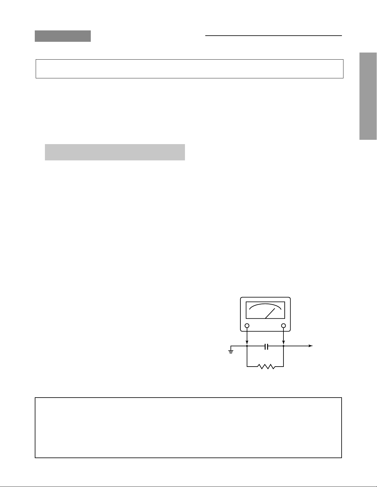
Connect a 1500 ohm 10 watt resistor , paralleled b y a 0.15
µF, AC type capacitor, between a known good earth ground
(water pipe, conduit, etc.) and the exposed metallic parts,
one at a time. Measure the AC voltage across the combination of 1500 ohm resistor and 0.15 µF capacitor. Reverse the AC plug at the AC outlet and repeat AC voltage
measurements for each exposed metallic part. Voltage
measured must not exceed 0.3 volts rms. This corresponds
to 0.2 milliamp. AC. Any value exceeding this limit constitutes a potential shock hazard and must be corrected immediately.
AC VOLTMETER
0.15µF
Place this probe on
Good earth ground
such as a water
pipe, conduit, etc.
1500 ohm
10 watt
each exposed
metallic part.
GENERAL ADJUSTMENTS
SPECIFIC INFORMATIONS
Many electrical and mechanical parts in this chassis have special safety-related characteristics. These characteristics are
often passed unnoticed by a visual inspection and the protection afforded by them cannot necessarily be obtained b y using
replacement components rated for higher voltage, w attage, etc. Replacement parts which have these special saf ety characteristics are identified in this manual and its supplements; electrical components having such features are identified by the
international hazard symbols on the schematic diagram and the parts list.
Before replacing any of these components, read the parts list in this manual carefully. The use of substitute replacement
parts which do not have the same safety characteristics as specified in the parts list may create shock, fire, X-ray radiation or other hazards.
– 3 –
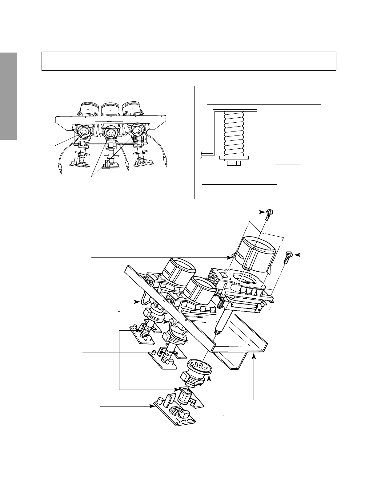
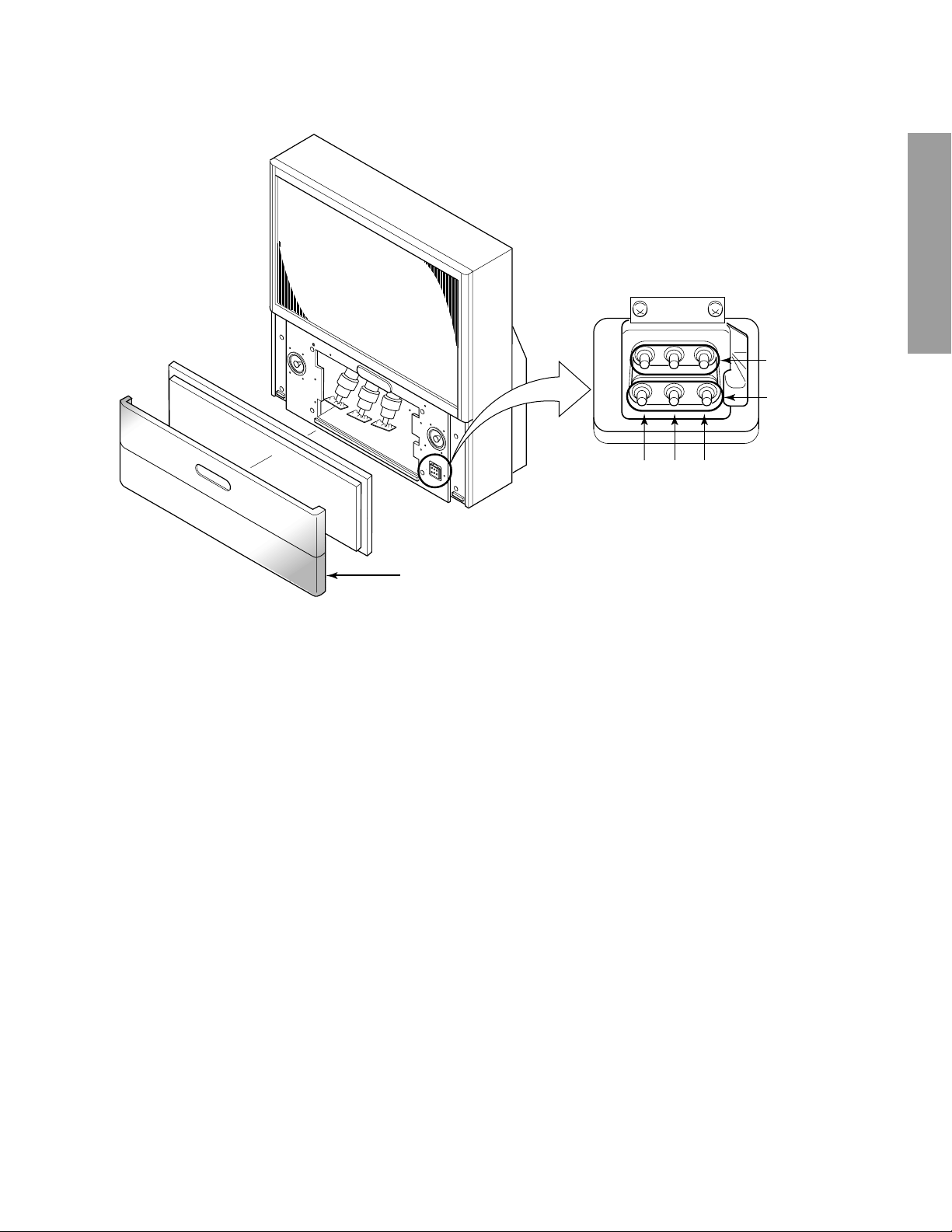
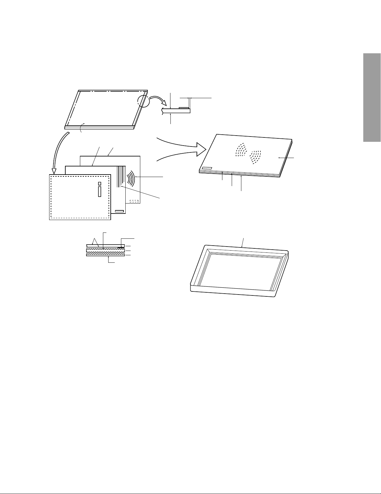
CRT ASSEMBLY REPLACEMENT AND MOUNTING
CAUTION : DO NOT LOOSEN THE HEX HEAD BOLTS WITH SPRINGS (12 PCS), BECAUSE THOSE ARE FOR
SEALING OF CRT COOLANT.
GENERAL ADJUSTMENTS
8 o’clock
4 o’clock
SPECIFIC INFORMATIONS
Lens Assembly
R
GB
Attention Serviceman
The Hex Head
Bolts with
Springs. (see
sketch) used on
CRT assembly,
are “NOT”
Adjustment Screws
DO NOT LOOSEN-FLUID
LEAKAGE WILL OCCUR.
4 Screws
4 Screws
CRT Assembly
CRT Anode Cap Assembly
S.V.M. Coil
CRT DRIVE Board
CRT Mounting
Deflection Yoke and Conver Yoke
Lens and Neck Components View
– 4 –
TO REMOVE CRT (Same procedure for R, G, B)
1. Remove CRT DRIVE Board, S. V. M. COIL and
DEF. YOKE from CRT.
2. Remove Lens Assembly.
3. Detach CRT Anode Cap from CRT.
4. Remove CRT Assembly from CRT Mounting.
CRT REPLACEMENT (Same procedure for R, G, B)
Reverse the removal procedures except the followings.
1. Anode Cable should be replaced with new one.
See “SERVICING PRECAUTIONS” shown below.
2. Install silicon (T461B) to the CRT, replace the Anode
cable and put enough silicon again on around the Anode Cap as illustrated.
CAUTION: Align the Anode cable as illustrated on page
4.
ADJUSTING PROCEDURE IN REPLACING CRT
1. R.G.B. FOCUS ADJUSTMENT (page 6.)
2. PICTURE TILT ADJUSTMENT (page 6.)
3. USER CONVERGENCE CENTER CHECK
(See owner's manual.)
4. CENTERING ADJUSTMENT (page 6.)
5. CONVERGENCE ADJUSTMENT (page 13.)
6. WHITE BALANCE ADJUSTMENT (page 12.)
Adjustments are complete.
Anode Cap
GENERAL ADJUSTMENTS
Silicon
(On shaded area)
TSE3843W #23960136
SERVICING PRECAUTIONS
■ Do not use a magnetized screw driver for screws
of Deflection Yoke and Velocity Modulation Coil to
avoid magnetization of electron gun.
Magnetization of electron gun will degrade basic
function and result in unbalance of right and left
shift of user static convergence, and result in no
variable quantity.
2 ~ 5 mm
SPECIFIC INFORMATIONS
15 ~ 25 mm
■ When replacing the anode cap assembly (CRT) or
anode lead assembly (F.B.T.), remove the anode
lead holder from old one and attach the holder
again to new anode lead.
■ Check the point of anode lead in a straight
line, if it is winding, please revise it.
Screw for
D.Y
Screw for SVM coil
Anode lead holder
– 5 –
WARNING : BEFORE SERVICING THIS CHASSIS , READ THE “X-RAY RADIA TION PRECA UTION”, “SAFETY PRE-
CAUTION” AND “PRODUCT SAFETY NOTICE” ON PAGE 3 OF THIS MANUAL.
PICTURE TUBE COMPONENTS ADJUSTMENT
DESCRIPTION OF NECK COMPONENTS
GENERAL ADJUSTMENTS
Deflection yoke and convergence yoke
The position on the neck is required most front (CRT
funnel side) and the screw is fastened after rotating
yoke adjusting picture tilt.
Centering magnet
After adjusting picture tilt, picture position is finally
fixed by this magnet.
In order to get maximum margin of user convergence
SPECIFIC INFORMATIONS
control for center of screen, this magnet have to be
used for center convergence adjustment.
PREPARATION
Operate the receiver for at least 5 minutes.
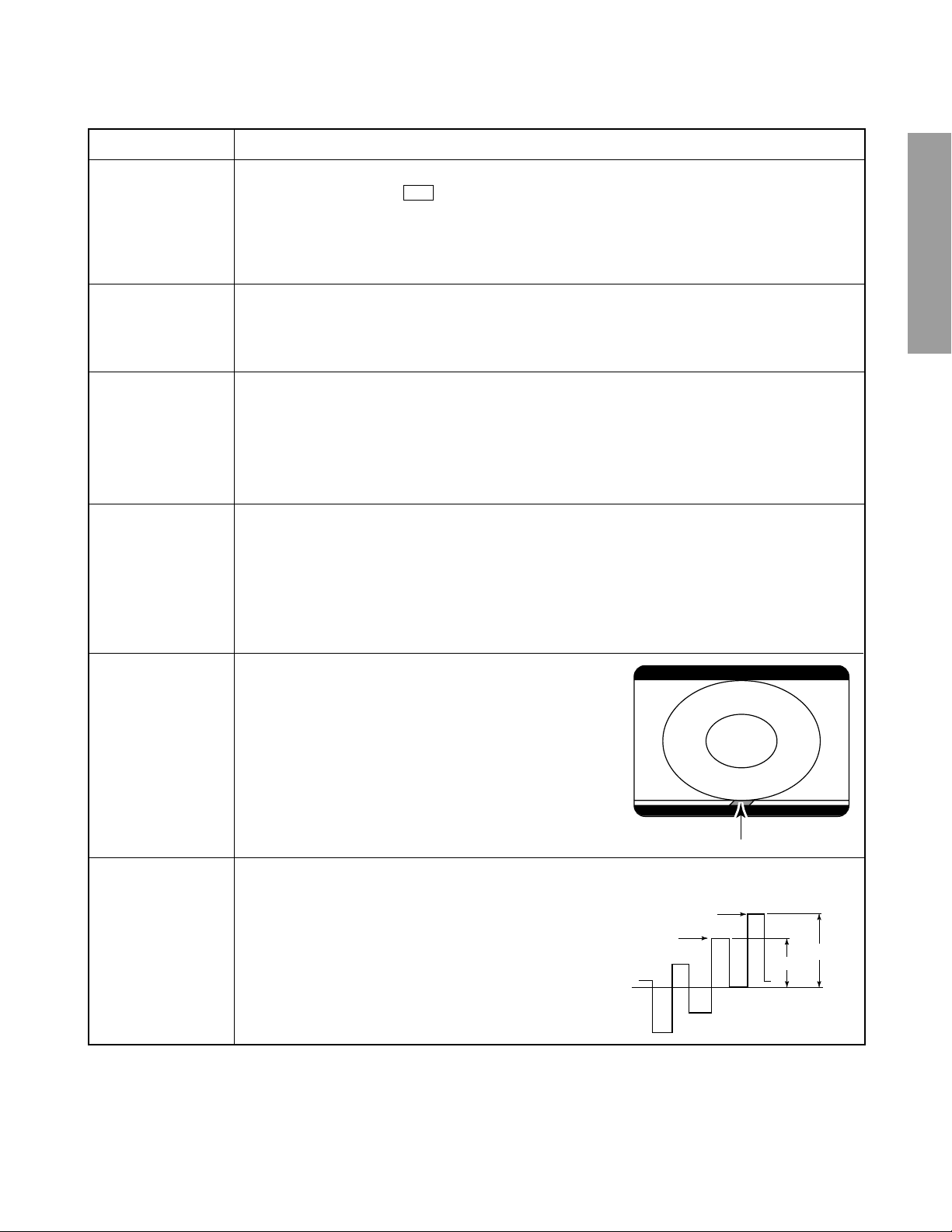
R, G, B FOCUS ADJUSTMENT
1. Before adjusting the R, G, B FOCUS, remov e the 4 screws
of Lens Assembly which is fixed on the CRT Assembly.
(See page 4.)
Then turn around the Lens Assembly by 180˚ to adjust
the fastening screw (Fig. a) and fasten the 4 screws to
secure Lens Assembly.
2. Select the adjustment mode. (See page 9.)
3. Press “7” button to display the built-in cross-hatch.
4. Press “0” and “RTN” buttons to make the picture a single
Red color.
100 button ............... to erase Red color
0 button ............... to erase Green color
CH RTN button ............... to erase Blue color
5. Loosen the fasten screw and adjust Red lense focus to
best focusing point of picture center . Then fasten the scre w.
(See Fig. a.)
TILT ADJUSTMENT
Rotate R, G, B deflection yoke so that picture becomes horizon, then fasten screw.
CENTERING ADJUSTMENT
1. Stretch a thread between two center of screen edge (top
and bottom, left and right).
2. Select the adjustment mode.
3. Press TV/VIDEO button on the Remote Control to displa y
the white cross-bar.
4. Perform VCEN adjustment. (See page 11.)
5. Adjust G centering magnet so that the cross-bar pattern
center comes to screen center.
6. Perform HEIGHT adjustment . (See page 12.)
7. Perform VERT. LINEARITY adjustment.
8. Perform WIDTH adjustment. (See page 11.)
9. Check whole quality of green line.
10
. Adjust R, B centering magnet so that the cross-bar pat-
tern center comes to screen center.
Fig. a
6. Adjust FOCUS VR “R” of FOCUS PACK to find best fo-
cusing point of picture center.
7. Repeat steps 3 to 5 for Green and Blue colors.
– 6 –
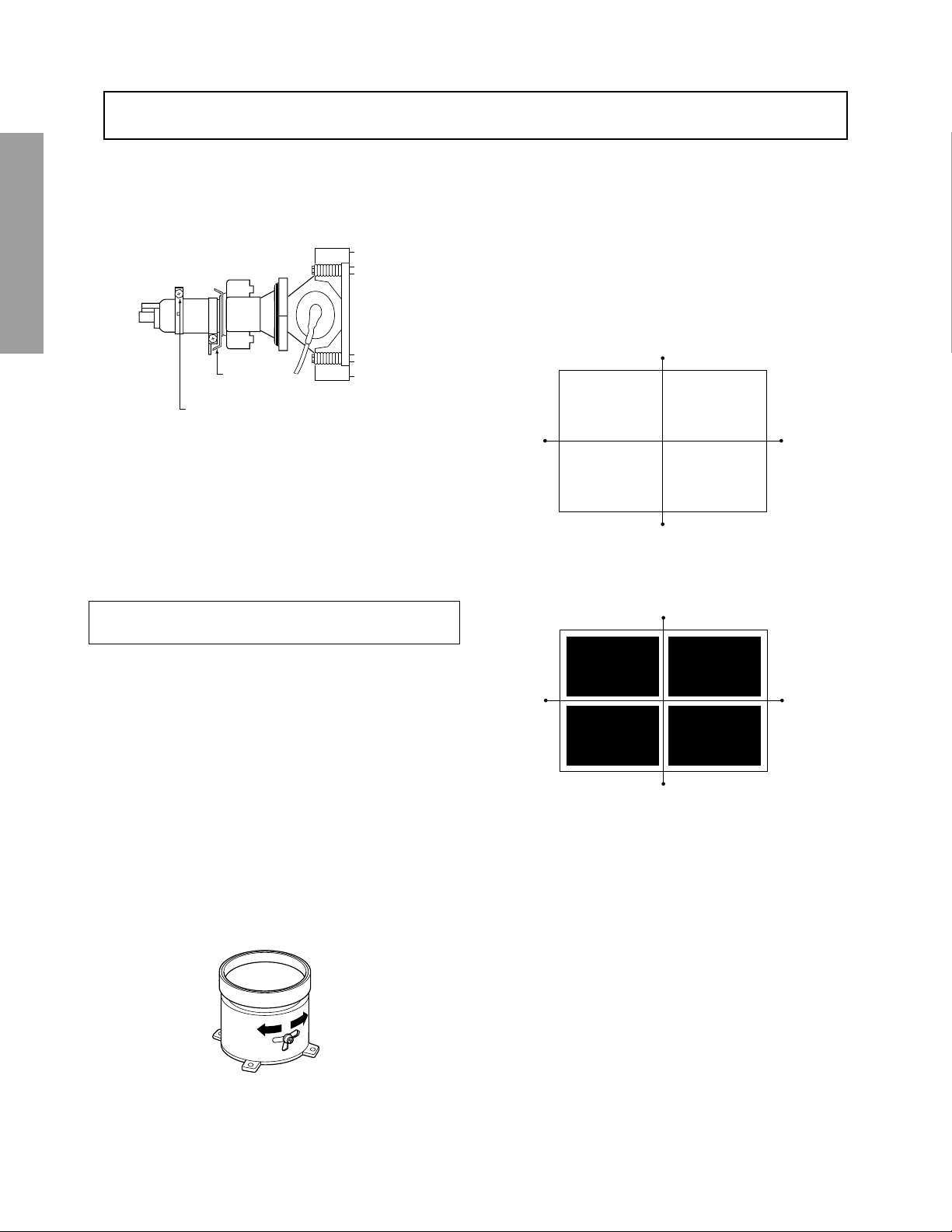
LOCATION OF SCREEN AND FOCUS VR’S
GENERAL ADJUSTMENTS
SCREEN VR
FOCUS VR
RGB
Speaker grille
SPECIFIC INFORMATIONS
– 7 –
REPLACEMENT OF THE CRT
Service parts are provided for each R, G and B.
The contents of the parts are as follows.
HITACHI
CRT 23008174 23008175 23008176
RGB
GENERAL ADJUSTMENTS
REPLACEMENT OF HIGH VOLTAGE CABLE
ANODE LEAD
RUBBER BOOT
LEAD HOLDER
SPECIFIC INFORMATIONS
Fig. a
Z450 TP A5007
1. When replacing Anode Lead or Anode Cap with ne w one,
remove Lead Holder from old lead as shown in figure
below, and put it on new lead. Do not throw away Lead
Holder.
NOTE : THE LEAD HOLDER IS ATTACHED TO TPA5007
(Z450), BUT IS NOT ATTACHED TO ANODE
LEAD AND ANODE CAP. RUBBER BOOT IS ATTACHED TO ANODE LEAD AND ANODE CAP.
2. Detaching Lead Holder
RUBBER BOOT
LOCK LEAD HOLDER
Fig. b
Cut here rubber boot
and lead together to
detach Lead Holder.
OLD
ANODE LEAD
or
ANODE CAP
– 8 –
1. ENTERING TO SERVICE MODE
1) Press MUTE button twice
on Remote Control.
SERVICE MODE
2) Press MUTE button
again to keep pressing.
3) While pressing the MUTE button,
press MENU button on TV set.
S
1/2 MUTE
MUTE
2. DISPLAYING THE ADJUSTMENT MENU
1) Press MENU button on TV.
Service mode
S
Press
Press
Adjustment mode
3. KEY FUNCTION IN THE SERVICE MODE
The following key entry during display of adjustment menu provides special functions.
Screen adjustment mode ON/OFF: TV (ANT)/VIDEO button (on TV)
Selection of the adjustment items : Channel s/t (on TV or Remote)
Change of the data value : Volume s/t (on TV or Remote)
Adjustment menu mode ON/OFF : MENU button (on TV)
Initialization of the memory (QA02) : RECALL+Channel button on TV (s)
Initialization of the self diagnostic data: RECALL+Channel button on TV (t)
“RCUT” selection : 1 button
“GCUT” selection : 2 button
“BCUT” selection : 3 button
“SCNT” selection : 4 button
“SCOL” selection : 5 button
“TNTC” selection : 6 button
Convergence adj : 7 button
Test audio signal ON/OFF (1kHz) : 8 button
Self diagnostic display : 9 button
(Service mode display)
GENERAL ADJUSTMENTS
Item
Data
SPECIFIC INFORMATIONS
– 9 –
4. SELECTING THE ADJUSTING ITEMS
1) Every pressing of CHANNEL s button in the service mode changes the adjustment items in the order of table-2.
(t button for reverse order)
Refer to table-2 for preset data of adjustment mode.
(See SETTING & ADJUSTING DATA on page 17)
5. ADJUSTING THE DATA
1) Pressing of VOLUME s or t button will change the value of data in the range from 00H to FFH. The variable range
depends on the adjusting item.
6. EXIT FROM SERVICE MODE
1) Pressing POWER button to turn off the TV once.
■ INITIALIZATION OF MEMORY DATA OF QA02
GENERAL ADJUSTMENTS
After replacing QA02, the following initialization is required.
1. Enter the service mode, then select any register item.
2. Press and hold the RECALL button on the Remote, then press the CHANNEL s button on the TV . The initialization of QA02
has been complated.
3. Check the picture carefully. If necessary, adjust any adjustment item above.
Perform “Programming Channel Memory” on the owner's manual.
CAUTION: Never attempt to initialize the data unless QA02 has been replaced.
7. SELF DIAGNOSTIC FUNCTION
1) Press “9” button on Remote Control during display of adjustment menu in the service mode.
The diagnosis will begin to check if interface among IC’s are executed properly.
2) During diagnosis, the following displays are shown.
SPECIFIC INFORMATIONS
Part number of microprocessor (QA01)
Operation number of protection circuit (current limiter) . . . . “000” is normal.
BUS line check “OK” ................... Normal
BUS line ACK (acknowledge) check
Sync. signal check Green display..... Normal
ID code for TV Set
Version of "EEP"
Data for "OPT"
SELF CHECK
NO. 23 * * * * * *
POWER : 000
BUS LINE : OK
BUS CONT : OK
BLOCK : MAIN SUB
SET ID : 01
EEP VER : 02
OPT1 : 05 OPT2 : 70
“SCL-GND” or “NG” ........... SCL-GND short circuit
“SDA-GND” or “NG” ........... SDA-GND short circuit
“SCL-SDA” or “NG” ............ SCL-SDA short circuit
“OK” ..................... Normal
Display of Location Number . . . . NG
(Display example)
“QA02 NG”, “H001 NG”, “Q501 NG” etc.
Note: The indication of failure place is only one place though failure places are plural. When
repair of a failure place finishes, the next failure place is indicated. (The order of priority of
indication is left side.)
Red display ........ NG
MAIN ........ Main sync
SUB .......... Sub sync (when turn on the PIP)
– 10 –
ELECTRICAL ADJUSTMENT
ITEM ADJUSTMENT PROCEDURE
ƒH
(free-running frequency of Hor.
oscillator)
VERTICAL POSITION (VCEN)
PICTURE POSITION
(HPOS)
WIDTH
(WID)
1. Receive NTSC signal.
2. Short the terminal “TP +9V ” and the terminal “ TP (F ree run) ” on the signal board with a jumper
wire.
3. Connect the probe of frequency counter to the lead of R426 and GND.
4. Adjust the frequency to “33.75±0.2 kHz” by turning R4034 on DPC Board.
5. Disconnect the shorted wire, then confirm that the picture is synchronized.
1. Receive NTSC signal.
2. Connect he probe of digital voltmeter to TP-V and TP-G on SIGNAL Board.
3. Call up the adjustment mode display, then select the item VCEN.
4. Press the VOLUME s or t button to get the voltage 0±10 mV.
1. Receive NTSC signal.
2. Call up the adjustment mode display.
3. Select the item “HPOS”, and adjust the data to “80H”.
4. Adjust the picture position alternately by turning CENTERING MAGNETS for proper picture
position.
5. Check the picture with off-air signal.
1. Receive NTSC signal.
2. Select the "FULL" mode by PIC SIZE button on Remote Control.
3. Call up the adjustment mode display, then select the item WID.
4. Press the VOLUME s or t button to get the picture so that left and right eddes of video signal
begin to lack.
5. Press the VOLUME s button to advance the data by 8 steps.
NOTE: Check the horizontal picture position is correct.
GENERAL ADJUSTMENTS
SPECIFIC INFORMATIONS
SUB-BRIGHTNESS
(BRTC)
SUB-COLOR
(SCOL)
1. Constrict the picture height until the vertical retrace line
appears adjusting the HEIGHT control on the MAIN board.
2. Adjust the CONTRAST to the minimum and BRIGHTNESS
to the center.
3. Enter the service mode, then select “BRTC” register.
4. Adjust the data value so the belt of vertical retrace line just
disappear.
5. Adjust the CONTRAST for the desired contrast.
6. Adjust the HEIGHT control.
Vertical retrace line
1. Receive color-bar signal from color-bar generator.
2. Adjust the BRIGHTNESS and CONTRAST to the center (RESET status).
3. Connect oscilloscope to TP501on the MAIN board.
4. Enter the service mode, then select “SCOL”.
5. Adjust the data value to achieve 1.8V
of blue bar on
0-p
Magenta
Blue
scope.
6. Check the picture with off-air signal.
0
2
3 (1.8V
0-P
)
– 11 –
ITEM ADJUSTMENT PROCEDURE
HEIGHT
(HIT)
VERTICAL LINEARITY
(VLIN)
(FULL mode only)
GENERAL ADJUSTMENTS
WHITE BALANCE
(RCUT)
(GCUT)
(BCUT)
(RDRV)
SPECIFIC INFORMATIONS
(BDRV)
1. Receive NTSC signal.
2. Select the "FULL" mode by PIC SIZE button on Remote Control.
3. Call up the adjustment mode display and select the item HIT.
4. Press the VOLUME s or t button to get the picture so that top and bottom of
video signal begin to lack.
5. Press the VOLUME s button to advance the data by 8 steps.
Note: Check the vertical picture position is correct.
Adjust the data of height after vertical linearty.
1. Receive cross-hatch pattern.
2. Call up the adjustment mode display, then select the item VLIN.
3. Press the VOLUME s or t button to obtain
the picture of the best linearity.
4. Then readjust the item HIT.
1. Press RESET button on TV or remote hand set.
2. Call up the adjustment mode display, then adjust the data of items RCUT, GCUT
and BCUT to “80”.
3. Press TV (ANT)/VIDEO button on TV.
4. Gradually rotate R, G and B SCREEN volume of FOCUS PAC (page 8) clockwise or counterclockwise until the raster appears slightly on the CRT through
the each lens, and leave them.
(Look into the lens in order to check the raster.)
5. Press TV (ANT)/VIDEO button on TV again.
6. Exit from service mode.
7. Receive white laster pattern signal, and adjust the contrast to the minimum to
make white picture to low light.
8. Adjust the data of items RCUT, GCUT and BCUT for low light area.
9. Adjust the contrast to the maximum to make white picture to high light.
10. Adjust the data of items RDRV and BDRV Controls for proper white-balanced
picture in high light area.
11. Check the white balance in both low and high light areas. If necessary, perform
again steps from 7 to 9.
– 12 –
CONVERGENCE ADJUSTMENT
Adjust convergence from center to circumf erence in order.
KEY FUNCTION IN THE CONVERGENCE ADJUSTMENT:
Up : 2 button
Selet Green color: 3 button
Left : 4 button
Blinking of cursor ON/OFF: 5 button
Right: 6 button
Adjust mode ON/OFF: 7 button
Down: 8 button
Vertical stripe ON/OFF 9 button
Erase Green line: 0 button
Erase Red line: 100 button
Erase Blue line: ENT button
Note:
Adjusting procedure in replacing convergence board.
1. User convergence center check. Make sure the best
convergence setting is about the center of adjustable
range.
2. CENTERING ADJUSTMENT
3. PICTURE POSITION ADJUSTMENT
4. HIT , WID ADJUSTMENT
5. CONVERGENCE ADJUSTMENT
6. Execute TOUCH FOCUS f ollowing instructions displa yed
on the screen after finishing CONVERGENCE ADJUSTMENT.
7. If TOUCH FOCUS ERROR is displayed after finishing
TOUCH FOCUS, the method of CROSS-HATCH PATTERN after CONVERGENCE adjustment is different from
what is exhibited on the right figure, or HARD WARE is out
of order.
1. Select the adjustment mode following the steps on page
9.
RCUT
40H
2. Press “7” button to display the built-in cross-hatch pattern
and press "9" button to display the vertical stripes.
Cursor
X: I
Y: I
FULL
C: R
FULL
3. Adjustment around cursor can be done.
The pattern includes three colors (R, G, B).
The cursor should be blinking in Red.
This means that the Red color is adjustable.
4. Press “3” button to select Green color to be adjusted.
5. Press “5” button to stop the blinking of cursor.
6. Press “2 (up)”, “8 (down)”, “4 (left)” or “6 (right)” to obtain
the correct cross-hatch pattern as above.
If necessary, the specified color line can be erased from
the screen.
100 button ...................... to erase Red line
0 button ...................... to erase Green line
CH RTN button ...................... to erase Blue line
7. Press “5” button to make the cursor blinking.
8. Press “2”, “8”, “4”, “6” buttons to move the cursor to other
point to be adjusted.
9. Repeat steps 5 to 8.
10.Repeat steps 4 to 9 to adjust Red and Blue colors.
Converge the selected color line into the Green line.
11.Press “7” button to memorize the adjusted states.
At this time, picture changes for about 1 second.
12.Press the TOUCH FOCUS button when "PLEASE PUSH
TOUCH FOCUS" is displayed on the screen.
13.TOUCH FOCUS is executed.
14.It returns to the normal screen after displaying "TOUCH
FOCUS FINISHED".
GENERAL ADJUSTMENTS
SPECIFIC INFORMATIONS
– 13 –
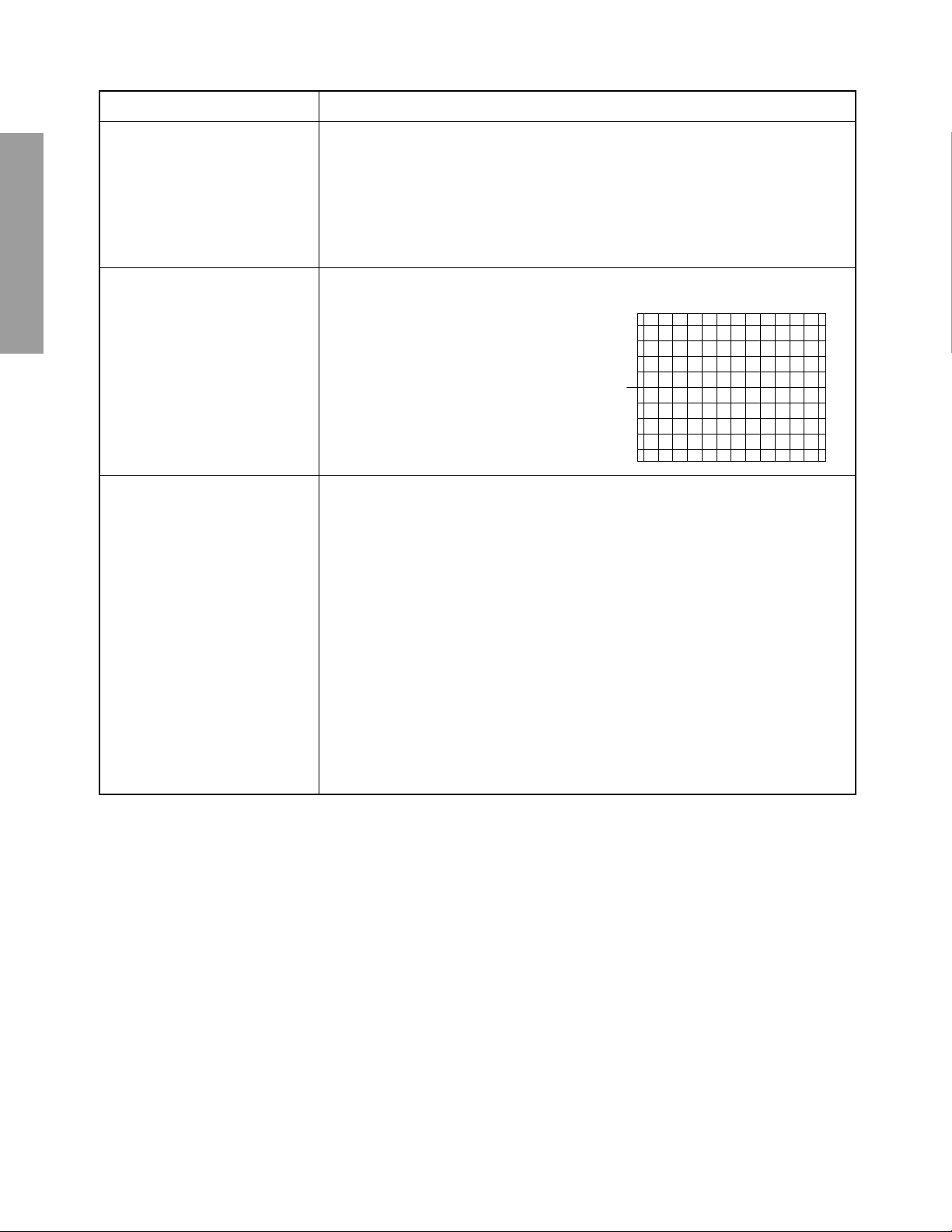
Adjusting Dimension of Each Picture Screen
(16:9 screen size:) 50 inches
(1) HD (1080I/NTSC)
GENERAL ADJUSTMENTS
22.0 531.0 442.5 265.5 088.5 88.5 265.5 442.5 531.0
50 inches 16:9 Screen size : Horizontal 1106 mm
NOTES
SPECIFIC INFORMATIONS
In many cases, color misconv ergence may be corrected b y returning HIT and WID data in main deflection side to initial adjusting
values. Following cases will surely require readjustment of convergence.
QH173,16KB CHIP, UFO–* BANK1 Vspan 38.8mm Hspan 88.5mm
271.5
233.0
116.5
Screen center
0
116.5
233.0
271.5
22.0
Vertical 622 mm
CRT REPLACEMENT
When CRT is replaced, main deflection readjustment and color matching are required.
Perform following procedures.
1. Replace two CRT’s of blue and red.
2. Perform horizontal adjustment for blue and red yokes on base of green CRT data. Mount yoke and velocity mod. coil alignment, pushing towards CRT without gap.
3. Adjust alignment of blue and red. (Refer Alignment adjustment for details.)
4. Rotating centering magnet, adjust CRT centers of red and blue to CRT center of green.
(Picture position adjustment)
5. Adjust HIT and WID data of main deflection, and decide data at the most precise screen comparing to green data.
6. Adjust convergence of screen picture for color matching. Do not move green one at this time.
7. After convergence adjustment of screen picture finishes, replace green CRT.
For green CRT as well, repeat steps 2 to 5 above on bases of red and blue color matching to adjust convergence.
8. Execute TOUCH FOCUS following instructions displayed on the screen after finishing convergence adjustments of all the
colors.
Note: Press button "7" again after "PLEASE PUSH TOUCH FOCUS" has been displa yed. Then, TOUCH FOCUS will not be
executed, and the current state of convergence will be displayed.
REPLACING CONVERGENCE UNIT
When replacing convergence unit, picture screen require readjustment basically, but the following method allows process be
reduced considerably.
1. Replace the memory (Q713) on defective unit with memory on new unit. Mounting the unit on the SET after the above
working realizes picture screen before replacement immediately.
2. Mount unit which has old memories, on SET and turn it on. Screen shows whole picture looks lik e straightly shifted tow ards
vertical or horizontal direction.
3. Adjust again centers of green, red and blue with centering magnets.
4. Check picture screen for slight disparity of color and picture size. If necessary, add some adjustments of main deflection and
color matching of convergence.
5. Execute TOUCH FOCUS following instructions displayed on the screen after finishing convergence adjustments of all the
colors.
Note: Press button "7" again after "PLEASE PUSH TOUCH FOCUS" has been displa yed. Then, TOUCH FOCUS will not be
executed, and the current state of convergence will be displayed.
– 14 –
SCREEN AND MIRROR ALIGNMENTS
ASSEMBLING OF FRONT SCREEN
K503 FRONT PANEL
LENTICULAR
K501
<OUTSIDE>
SMOOTH
K502
FRESNAL
BLACK STRIPES
SMOOTH
<INSIDE>
SPACER
FRONT PANEL
LENTICULAR
FRESNEL
INSIDE
OUT SIDE
LENS
BLACK STRIPES
0 to 1 mm
MOUNTING OF FRONT SCREEN
FRESNEL
LENTICULAR
FRONT PANEL
BEZEL
GENERAL ADJUSTMENTS
SMOOTH
SPECIFIC INFORMATIONS
CAUTION : Do not hold the optical system parts (lens and
mirror) with bare hand to avoid finger-prints on
the surface of those parts.
HOW TO CLEAN LENS AND MIRROR
1. Be sure to remove sand dust with an air brush, etc.
2. When it is stained slightly, breathe upon it and wipe away
with the specified cleaning cloth.
For other stains than the above , wipe the stains awa y with
the specified cloth into which a cleaning liquid has been
soaked.
Cleaning liquid.................... LENS LUSTER (Manufac-
tured by Edmund Scientific
Co.), etc.
HOW TO CLEAN SCREEN
When cleaning the screen, use a soft cloth so as not to
damage the screen.
1. Wipe the screen with a dry cloth to remove moisture on
the screen.
Note : Absolutely do not use detergent, water, alcohol,
benzine, thinner, etc. for cleaning in order not to
wipe away the black print on the surface.
– 15 –
CIRCUIT CHECKS
HIGH VOLTAGE CHECK
CAUTION: There is no HIGH VOLTAGE ADJUSTMENT on
this chassis. Checking should be done following
the steps below.
1. Connect an accurate high voltage meter to the anode of
the picture tube.
2. Turn on the receiver. Set the BRIGHTNESS and CONTRAST to minimum (zero beam current).
3. High voltage must be measured below (B) kV.
Refer to table-1 for high voltage (B).
(See SETTING & ADJUSTING DATA on page 17)
GENERAL ADJUSTMENTS
SPECIFIC INFORMATIONS
4. Var y the BRIGHTNESS to both extremes to be sure the
high voltage does not exceed the limit under any conditions.
CAUTION:
When the following parts fail, check the High Voltage after
replacing.
Location
No.
T461
C407
C408
C441
C432
C433
Name
Flyback
Capacitor
Capacitor
Capacitor
Capacitor
Capacitor
Descriptions
50"
TFB3090AD
4700pF, ±3%
8200pF, ±5%
4700pF, ±5%
8200pF, ±5%
1200pF, ±3%
FS CIRCUIT CHECK
The Fail Safe (FS) circuit check is indispensable for the final
check in servicing. Checking should be done following the
steps below.
1. Turn the receiver on.
2. T emporarily short TP- (R) and TP- (X) on the DEF/POWER
Board with a jumper wire.
Raster and sound will disappear.
3. The receiver must remain in this state e ven after removing
the jumper wire. This is the evidence that the FS circuit is
functioning properly.
4. To obtain a picture again, temporarily turn the receiver off
and allow the FS circuit more than 5 seconds to reset. Then
turn the receiver on to produce a normal picture.
Troubleshooting Guide for Fail Safe Circuit
Check that the set returns to normal operation when
pin 12 of Z801 is grounded with jumper wire.
YES NO
Check the voltage across
Capacitor C419 is
approximately (
Refer to table –4 for
fall safe voltage (
C)
volts.
C)
.
Faulty power
circuit or horizontal circuit.
ANODE VOLTAGE MEASURING METHOD
CAUTION: Take extra precaution when measuring this high
voltage. High voltages are also present in
surrounding circuit boards (CRT DRIVE assembly, DEFLECTION assembly, and POWER
SUPPLY assembly).
1. Disconnect the FBT anode cable as outlined below . Measure high voltage at the point where the cable enters the
FBT.
2. Holding the rubber cover firmly, turn it counterclockwise
and check that the lock has been disengaged. (See Fig. b
on page 8.)
3. Determine the extent of the rubber cover before disconnecting the cable.
4. Pull straight up the anode cable to disconnect.
5. When reconnecting the cable, proceed in the reverse order .
After reconnecting, tug on the cable to check that it is secure.
YES
Defective Fail Safe Circuit
(See SETTING & ADJUSTING
DATA on page 17)
NO
– 16 –
CHAPTER 2 SPECIFIC INFORMATIONS
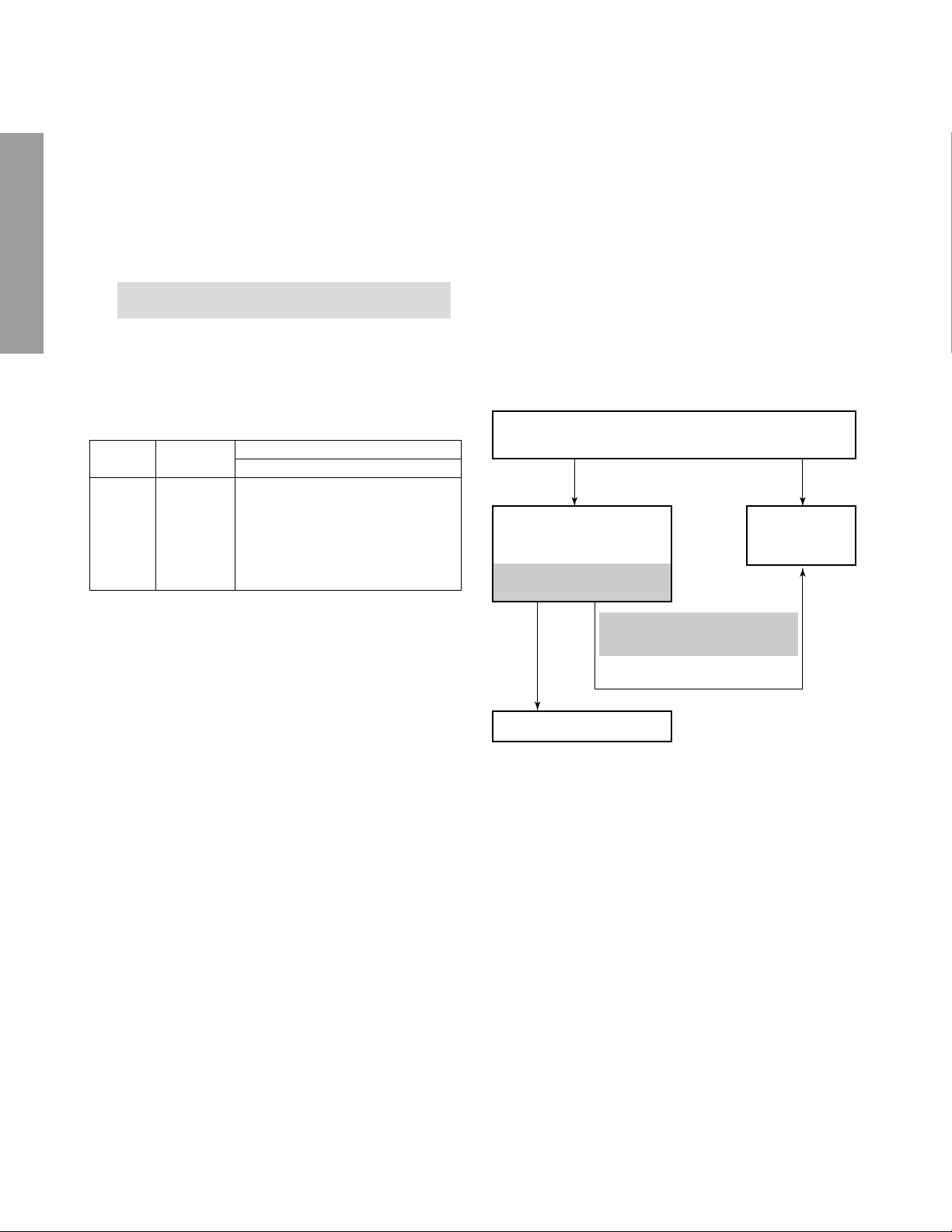
SETTING & ADJUSTING DATA
SAFETY INSTRUCTIONS
HIGH VOLTAGE AT ZERO BEAM: (A) 31.0 kV
MAX HIGH VOLTAGE:
Table-1
SERVICE MODE
50"
(B) 32.5 kV
ADJUSTING ITEMS AND DATA IN THE SERVICE MODE:
Item Name of adjustment
RCUT
GCUT
BCUT
RDRV
BDRV
BRTC
TNTC
SCOL
SCNT
HPOS
VPOS
HIT
LIN
VSC
WID
VPS
EYOF
ECNT
R CUTOFF
G CUTOFF
B CUTOFF
R DRIVE
B DRIVE
SUB-BRIGHT
SUB-TINT
SUB COLOR
SUB-CONTRAST
HORIZ. POSITION
VERT. POSITION
HEIGHT
V-LINEARITY
V-S CORRECTION
PICTURE WIDTH
V-SHIFT
Y1 BLACK (Q501)
Y1 SCONT (Q501)
Preset Data
40H
40H
40H
40H
40H
80H
44H
05H
10H
80H
19H
38H
12H
10H
1DH
0AH
07H
16H
←
←
←
←
←
←
←
←
←
←
←
55H
←
←
←
←
←
←
Item Name of adjustment Preset Data
EIOF
EQOF
PYOF
PIOF
PQOF
VCP
PARA
CNR
HCP
VFC
PHUE
PCNT
PCOL
RGBB
VCEN
TVOP
OPT0
OPT1
R-Y BLACK (Q501)
R-Y BLACK (Q501)
PIP Y OFFSET
PIP I OFFSET
PIP Q OFFSET
V-COMPENSATE
E-W PARABOLA (DPC)
E-W CORNER
H-COMPENSATE
V-F CORRECT
PIP TINT
PIP CONT
PIP COLOR
RGB BRIGHT
V POSITION
TV OPTION
TV SET OPTION
TV SET OPTION
20H
20H
17H
24H
1EH
0AH
17H
08H
00H
00H
40H
10H
15H
54H
70H
08H
50H
05H
←
←
←
←
←
←
←
←
←
←
←
←
←
←
←
18H
←
←
GENERAL ADJUSTMENTS
SPECIFIC INFORMATIONS
CIRCUIT CHECKS
Table-2
FBT DETECTION VOLTAGE (C) 24.5 V
HIGH VOLTAGE DET 8.7 V
Table-3
– 17 –
TV front
GENERAL ADJUSTMENTS
LOCATION OF CONTROLS
Remort sensor
(Behibd the screen)
Channel ts
Volume T S
Menu tsT S
Automatic Light Sensor
SPECIFIC INFORMATIONS
TV rear
Video 3
Video/audio inputs
(behind the door)
S-VIDEO
VIDEO
L/
MONO
AUDIO
R
VIDEO-2VIDEO-1
COLOR
STREAM
HD-1
MENU
R
Y
P
B
P
R
AUDIO
CHs
VOL TSVOL
CHt
OUT
L
VAR
AUDIO
VIDEO
L/
L
MONO
AUDIO
R
R
OUTININ
EXIT
AUDIO CENTER
CHANNEL IN
ON OFF
Y
P
B
AUDIO
P
R
COLOR
STREAM
HD-2
IN
TV/VIDEO
TOUCH FOCUS
ANT (75Ω)
L
R
POWER
POWER
Power indicator
ANT-1
OUT
ANT-2
– 18 –
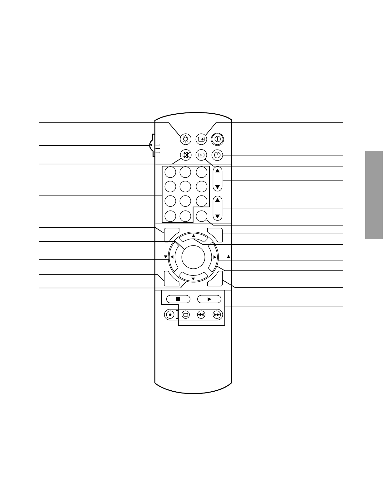
Remote Control
LIGHT
TV/CABLE/VCR switch
Set to “TV” to control the TV.
MUTE
Channel Number
FAVORITE
ENTER
FAV t
C. CAPT
POP CH t
TV
CABLE
VCR
1
4
7
100
FAVORITE
FAV
C. CAPT
STOP SOURCE
REC
RECALL
3
6
9
CH RTN
ENT
PLAY POP
POWER
TIMER
CH
VOL
PIC SIZE
EXIT
LIGHT
MUTE TV/VIDEO
2
5
8
0
ADV/
POP CH
MENU/
ENTER
ADV/
POP CH
TV/VCR REW FF
FAV
RECALL
POWER
TIMER
TV/VIDEO
CHANNEL s/t
VOLUME s/t
CH RTN
PIC SIZE
POP CH
s
FAV s
s/t/T/S
EXIT
POP functions
(For “TV” and “CABLE” modes)
GENERAL ADJUSTMENTS
SPECIFIC INFORMATIONS
STILL SWAP
– 19 –

PROGRAMMING CHANNEL MEMORY
The channel memory is the list of TV channel numbers the TV tunes in when you press the CHANNEL s or t button.
First, use the TV/CABLE and CH PROGRAM functions to preset all active channels in your area automatically.
If necessary, arrange the preset channels with the ADD/ERASE functions so that you can tune into only desired channels.
Note: If you utilize both ANT-1 and ANT-2 terminals for some model, perform programming channels for each input source.
TV/CABLE function
1 Press MENU, then press S or T until the SET UP menu
GENERAL ADJUSTMENTS
appears.
2 Press t (or s) until “TV/CABLE” is highlighted.
3 Press : or ; to highlight either “TV” or “CABLE”, whichever
you use.
CH PROGRAM function
1 Select “CH PROGRAM” following steps 1 and 2 above.
2 Press : or ; to start channel programming.
SPECIFIC INFORMATIONS
The TV will automatically cycle through all the TV or
CABLE channels selected by the TV/CABLE function, and
store active channels in the channel memory.
3 When channel programming is complete, you will see the
message to the right appears.
4 Press CHANNEL s or t to make sure the channel
programming has been done properly.
ADD/ERASE function
After performing the CH PROGRAM function, you can add or
erase specific channels.
1 Select the channel you want to erase using the CHANNEL
s or t button, or select the channel you want to add using
the Channel Number buttons.
2 Press MENU, then press S or T until the SET UP menu
appears.
3 Press t (or s) until “ADD/ERASE” is highlighted.
4 Press S or T :
To erase the channel press the button until “ERASE” is
highlighted.
To add the channel press the button until “ADD” is
highlighted.
5 Repeat steps 1 to 4 for other channels.
You have now completed the channel programming.
Note: The CHANNEL t/s buttons on the TV function as the
t/s buttons while a menu is on the screen.
* Please refer to owner's manual in detail.
– 20 –
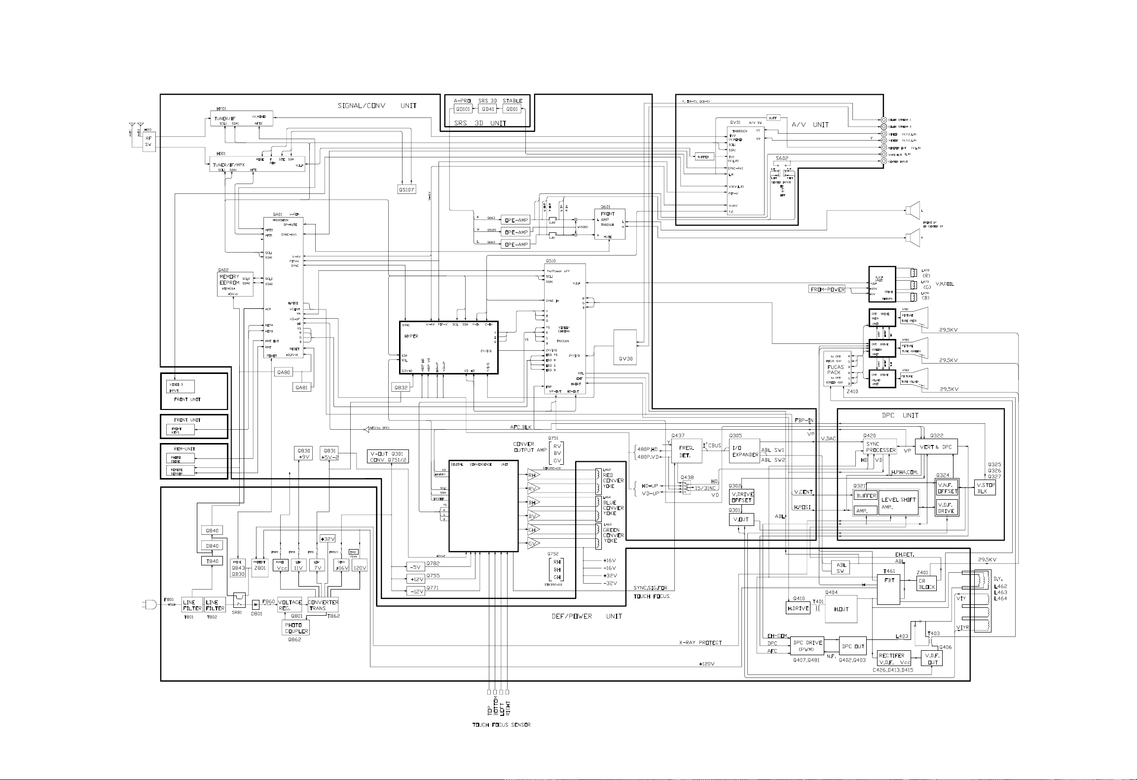
CIRCUIT BLOCK DIAGRAM
– 21 – – 22 –
50H81 Series
BLOCK DIAGRAM
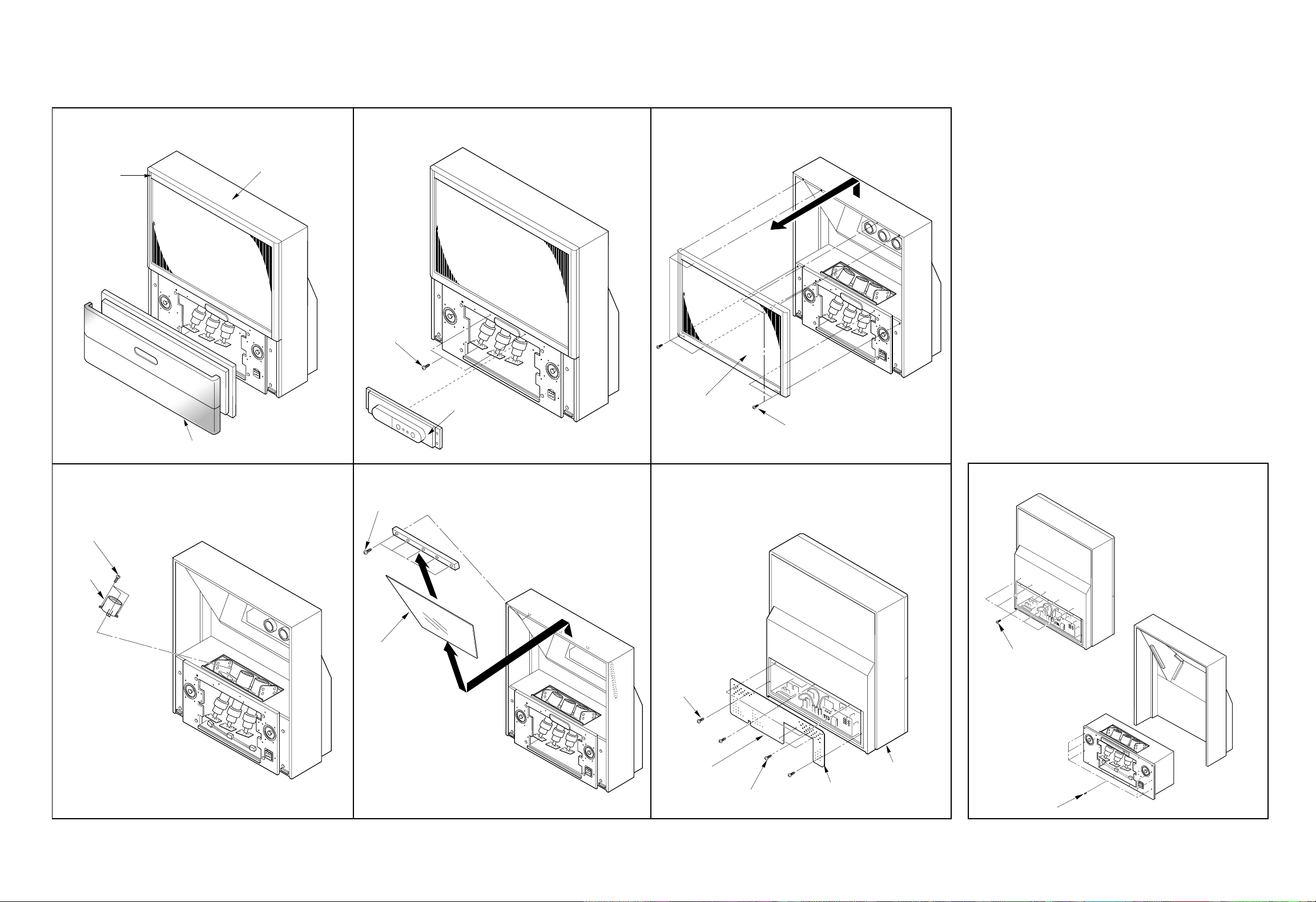
MECHANICAL DISASSEMBLY
A424
3 screws
A160
A421
5 screws
K501
K502
K503
8 screws
5 screws
6 screws
1 Speaker Grille Removal 2 Control Panel Removal
A268
A102
A101
2 screws
A202
A214
A213
A212
3 Front Mask Removal
4 Shield Plate, Lens Removal 5 Mirror Removal
5 screws
4 screws
K111
K112
K113
K601
6 Back Board Removal
7 Light Box Removal
– 23 –
– 24 –
CHASSIS REPLACEMENT PARTS LIST
WARNING: BEFORE SER VICING THIS CHASSIS, READ THE “X-RA Y RADIATION PRECAUTION”, “SAFETY PRE-
CAUTION” AND “PRODUCT SAFETY NOTICE” ON PAGE 3 OF THIS MANUAL.
CAUTION: The international hazard symbols “ ” in the schematic diag r am and the parts list designate components
which have special characteristics important for safety and should be replaced only with types identical to those in the
original circuit or specified in the parts list. The mounting position of replacements is to be identical with originals.
Before replacing any of these components, read carefully the PRODUCT SAFETY NOTICE. Do not degrade the
safety of the receiver through improper servicing.
NOTICE:
•
The part number must be used when ordering parts, in order to assist in processing, be sure to include the Model
number and Description.
•
The PC board assembly with * mark is no longer available after the end of the production.
Models : 50H81
Capacitors ............. CD : Ceramic Disk PF : Plastic Film EL : Electrolytic
Resistors ............... CF : Carbon Film CC : Carbon Composition MF : Metal Film
OMF : Oxide Metal Film VR : Variable Resistor FR : Fusible Resistor
(All CD and PF capacitors are ±5%, 50V and all resistors, ±5%, 1/6W unless otherwise noted.)
Location
No.
CAPACITORSCAPACITORS
CAPACITORS
CAPACITORSCAPACITORS
C102 24665221 EL, 220?F, ±20%, 10V
C105 24100102 Chip, 1000pF, +80%, -20%
C106 24669479 EL, 4.7?F, ±20%, 50V
C107 24666221 EL, 220?F, ±20%, 16V
C112 24665221 EL, 220?F, ±20%, 10V
C115 24100102 Chip, 1000pF, +80%, -20%
C117 24666221 EL, 220?F, ±20%, 16V
C201 24092730 Chip, 0.1?F, ±10%, 16V
C205 24206229 EL, 2.2?F, ±20%, 50V
C207 24105100 Chip, 10pF, ±0.5pF
C208 24105100 Chip, 10pF, ±0.5pF
C209 24105100 Chip, 10pF, ±0.5pF
C211 24092730 Chip, 0.1?F, ±10%, 16V
C212 24666100 EL, 10?F, ±20%, 16V
C221 24503041 PF, 0.1?F, 63V
C301 24617820 EL, 100?F, ±20%, 50V
C302 24669101 EL, 100?F, ±20%, 50V
C303 24109473 Chip, 0.047?F, ±10%, 25V
C304 24503053 PF, 1?F, 63V
C305 24082057 PF, 0.22?F, 100V
C306 24082260 PF, 4700pF, 100V
C307 24109333 Chip, 0.033?F, ±10%, 25V
C308 24617820 EL, 100?F, ±20%, 50V
C309 24693473 PF, 0.047?F, 100V
C311 24109471 Chip, 470pF, ±10%
C312 24666100 EL, 10?F, ±20%, 16V
C313 24666220 EL, 22?F, ±20%, 16V
C315 24619071 Chip, 2.2pF, ±20%
C321 24503041 PF, 0.1?F, 63V
C322 24567224 PF, 0.22?F
C323 24567224 PF, 0.22?F
C324 24073053 EL, 100?F, ±20%, 25V
C325 24503041 PF, 0.1?F, 63V
C326 24503041 PF, 0.1?F, 63V
C327 24567103 PF, 0.01?F
C328 24617912 EL, 2.2?F, ±10%, 50V
C329 24567183 PF, 0.018?F
C331 24212102 CD, 1000pF, ±10%
C332 24073020 EL, 1000?F, ±20%, 10V
C333 24567103 PF, 0.01?F
Part No. Description
Location
No.
C334 24591102 PF, 1000pF
C335 24567474 PF, 0.47?F
C336 24503041 PF, 0.1?F, 63V
C337 24212101 CD, 100pF, ±10%
C338 24073020 EL, 1000?F, ±20%, 10V
C339 24666101 EL, 100?F, ±20%, 16V
C341 24591222 PF, 2200pF
C342 24591222 PF, 2200pF
C343 24667101 EL, 100?F, ±20%, 25V
C344 24567393 PF, 0.039?F
C345 24503041 PF, 0.1?F, 63V
C346 24669100 EL, 10?F, ±20%, 50V
C347 24085946 EL, 10?F, ±20%, 16V,
C348 24567224 PF, 0.22?F
C349 24567224 PF, 0.22?F
C351 24503041 PF, 0.1?F, 63V
C352 24669229 EL, 2.2?F, ±20%, 50V
C353 24669010 EL, 1?F, ±20%, 50V
C354 24567823 PF, 0.082?F
C355 24567563 PF, 0.056?F
C356 24665101 EL, 100?F, ±20%, 10V
C357 24073037 EL, 47?F, ±20%, 16V
C401 24214332 CD, 3300pF, ±10%, 500V
C402 24092463 Chip, 0.22?F, ±10%, 16V
C403 24676220 EL, 22?F, ±20%, 100V
C404 24619071 Chip, 2.2pF, ±20%
C405 24567124 PF, 0.12?F
C406 24109223 Chip, 0.022?F, ±10%, 25V
* C407 24082608 PF, 4700pF, ±3%, 1800V
* C408 24820822 PF, 8200pF, 630V
C410 24105221 Chip, 220pF
C411 24678220 EL, 22?F, ±20%, 200V
C412 24828823 PF, 0.082?F, 200V
C413 24214221 CD, 220pF, ±10%, 500V
* C414 24082647 PF, 0.27?F, 400V
C415 24092484 CD, 1500pF, ±10%, 2kV
C416 24095716 PF, 1.5?F, ±10%, 250V
* C417 24082648 PF, 0.3?F, 400V
C418 24679330 EL, 33?F, ±20%, 250V
C420 24503041 PF, 0.1?F, 63V
Part No. Description
Non-Polar
SPECIFIC INFORMATIONS
– 25 –

Location
No.
Part No. Description
Location
No.
Part No. Description
C421 24640908 EL, 33?F, ±20%, 160V
C422 24591102 PF, 1000pF
C423 24211222 CD, 2200pF, ±10%, 2kV
C424 24828473 PF, 0.047?F, 200V
C426 24591153 PF, 0.015?F
C427 24567123 PF, 0.012?F
C428 24591102 PF, 1000pF
C429 24567333 PF, 0.033?F
C431 24591102 PF, 1000pF
* C432 24820822 PF, 8200pF, 630V
* C433 24082594 PF, 1200pF, ±3%, 1800V
C434 24073057 EL, 1000?F, ±20%, 25V
C435 24503041 PF, 0.1?F, 63V
C436 24503041 PF, 0.1?F, 63V
C437 24666331 EL, 330?F, ±20%, 16V
C438 24666101 EL, 100?F, ±20%, 16V
C439 24591223 PF, 0.022?F
* C441 24082608 PF, 4700pF, ±3%, 1800V
C451 24567223 PF, 0.022?F
C452 24073040 EL, 330?F, ±20%, 16V
C453 24109103 Chip, 0.01?F, ±10%
C454 24797010 EL, 1?F, ±20%, 50V
C455 24109103 Chip, 0.01?F, ±10%
C456 24085903 EL, 1?F, ±20%, 50V,
C457 24669010 EL, 1?F, ±20%, 50V
C458 24073039 EL, 220?F, ±20%, 16V
C459 24100104 Chip, 0.1?F, +80%, -20%, 25V
SPECIFIC INFORMATIONS
C460 24109103 Chip, 0.01?F, ±10%
C462 24105101 Chip, 100pF
C463 24109103 Chip, 0.01?F, ±10%
C464 24109103 Chip, 0.01?F, ±10%
C465 24109103 Chip, 0.01?F, ±10%
C467 24085903 EL, 1?F, ±20%, 50V,
C469 24073034 EL, 10?F, ±20%, 16V
C471 24503041 PF, 0.1?F, 63V
C472 24353100 CD, 10pF, ±0.25pF, CH
C473 24503041 PF, 0.1?F, 63V
C474 24501561 PF, 560pF
C475 24501272 PF, 2700pF
C476 24669479 EL, 4.7?F, ±20%, 50V
C477 24567103 PF, 0.01?F
C478 24591822 PF, 8200pF
C479 24669229 EL, 2.2?F, ±20%, 50V
C481 24669229 EL, 2.2?F, ±20%, 50V
C482 24501272 PF, 2700pF
C483 24501102 PF, 1000pF
C484 24503041 PF, 0.1?F, 63V
C485 24666331 EL, 330?F, ±20%, 16V
C486 24567103 PF, 0.01?F
C487 24501151 PF, 150pF
C488 24503041 PF, 0.1?F, 63V
C489 24666331 EL, 330?F, ±20%, 16V
C491 24591332 PF, 3300pF
C493 24436220 CD, 22pF
C496 24567474 PF, 0.47?F
C497 24073039 EL, 220?F, ±20%, 16V
C498 24073084 EL, 4.7?F, ±20%, 50V
C501 24109103 Chip, 0.01?F, ±10%
C502 24092730 Chip, 0.1?F, ±10%, 16V
C503 24619151 Chip, 47pF, 6.3V
C504 24109222 Chip, 2200pF, ±10%
C505 24105120 Chip, 12pF
Non-Polar
Non-Polar
C506 24105120 Chip, 12pF
C507 24105120 Chip, 12pF
C508 24100104 Chip, 0.1?F, +80%, -20%, 25V
C509 24619157 Chip, 10pF, 16V
C510 24092730 Chip, 0.1?F, ±10%, 16V
C511 24619157 Chip, 10pF, 16V
C512 24092463 Chip, 0.22?F, ±10%, 16V
C513 24100104 Chip, 0.1?F, +80%, -20%, 25V
C514 24619040 Chip, 10pF, ±20%, 16V
C518 24666100 EL, 10?F, ±20%, 16V
C524 24092730 Chip, 0.1?F, ±10%, 16V
C525 24092730 Chip, 0.1?F, ±10%, 16V
C526 24092730 Chip, 0.1?F, ±10%, 16V
C527 24092730 Chip, 0.1?F, ±10%, 16V
C528 24092730 Chip, 0.1?F, ±10%, 16V
C529 24092730 Chip, 0.1?F, ±10%, 16V
C530 24669010 EL, 1?F, ±20%, 50V
C531 24666101 EL, 100?F, ±20%, 16V
C532 24666100 EL, 10?F, ±20%, 16V
C535 24092730 Chip, 0.1?F, ±10%, 16V
C536 24109103 Chip, 0.01?F, ±10%
C537 24109103 Chip, 0.01?F, ±10%
C547 24109103 Chip, 0.01?F, ±10%
C551 24100104 Chip, 0.1?F, +80%, -20%, 25V
C552 24100104 Chip, 0.1?F, +80%, -20%, 25V
C553 24100104 Chip, 0.1?F, +80%, -20%, 25V
C554 24100104 Chip, 0.1?F, +80%, -20%, 25V
C555 24100104 Chip, 0.1?F, +80%, -20%, 25V
C556 24100104 Chip, 0.1?F, +80%, -20%, 25V
C563 24206229 EL, 2.2?F, ±20%, 50V
C564 24666100 EL, 10?F, ±20%, 16V
C565 24206229 EL, 2.2?F, ±20%, 50V
C566 24206229 EL, 2.2?F, ±20%, 50V
C567 24109103 Chip, 0.01?F, ±10%
C568 24109103 Chip, 0.01?F, ±10%
C569 24109103 Chip, 0.01?F, ±10%
C570 24669010 EL, 1?F, ±20%, 50V
C601 24109102 Chip, 1000pF, ±10%
C602 24109102 Chip, 1000pF, ±10%
C603 24669100 EL, 10?F, ±20%, 50V
C604 24669100 EL, 10?F, ±20%, 50V
C605 24667470 EL, 47?F, ±20%, 25V
C606 24667470 EL, 47?F, ±20%, 25V
C607 24503041 PF, 0.1?F, 63V
C608 24503041 PF, 0.1?F, 63V
C609 24669102 EL, 1000?F, ±20%, 50V
C610 24669102 EL, 1000?F, ±20%, 50V
C611 24667470 EL, 47?F, ±20%, 25V
C612 24666221 EL, 220?F, ±20%, 16V
C661 24206010 EL, 1?F, ±20%, 50V
C662 24206010 EL, 1?F, ±20%, 50V
C663 24206010 EL, 1?F, ±20%, 50V
C664 24669220 EL, 22?F, ±20%, 50V
C665 24109103 Chip, 0.01?F, ±10%
C666 24206010 EL, 1?F, ±20%, 50V
C667 24794100 EL, 10?F, ±20%, 16V
C680 24669471 EL, 470?F, ±20%, 50V
C681 24666100 EL, 10?F, ±20%, 16V
C682 24092538 Chip, 1?F, +80%, -20%, 10V
C683 24092538 Chip, 1?F, +80%, -20%, 10V
C690 24109103 Chip, 0.01?F, ±10%
C704 24232103 CD, 0.01?F, +80%, -20%
C705 24206479 EL, 4.7?F, ±20%, 50V
C707 24797470 EL, 47?F, ±20%, 50V
– 26 –

Location
No.
Part No. Description
Location
No.
Part No. Description
C712 24797470 EL, 47?F, ±20%, 50V
C713 24790470 EL, 47?F, ±20%, 160V
C715 24214472 CD, 4700pF, ±10%, 500V
C717 24214472 CD, 4700pF, ±10%, 500V
C718 24666470 EL, 47?F, ±20%, 16V
C719 24435560 CD, 56pF, 500V
C720 24790220 EL, 22?F, ±20%, 160V
C721 24666470 EL, 47?F, ±20%, 16V
C726 24212102 CD, 1000pF, ±10%
C760 24797470 EL, 47?F, ±20%, 50V
C761 24212102 CD, 1000pF, ±10%
C762 24797470 EL, 47?F, ±20%, 50V
C765 24214472 CD, 4700pF, ±10%, 500V
C766 24214472 CD, 4700pF, ±10%, 500V
C767 24790470 EL, 47?F, ±20%, 160V
C768 24666470 EL, 47?F, ±20%, 16V
C769 24666470 EL, 47?F, ±20%, 16V
C770 24435560 CD, 56pF, 500V
C771 24790220 EL, 22?F, ±20%, 160V
C780 24797470 EL, 47?F, ±20%, 50V
C781 24212102 CD, 1000pF, ±10%
C782 24797470 EL, 47?F, ±20%, 50V
C784 24214472 CD, 4700pF, ±10%, 500V
C786 24214472 CD, 4700pF, ±10%, 500V
C787 24790470 EL, 47?F, ±20%, 160V
C788 24666470 EL, 47?F, ±20%, 16V
C789 24666470 EL, 47?F, ±20%, 16V
C790 24435560 CD, 56pF, 500V
C791 24790220 EL, 22?F, ±20%, 160V
C792 24669229 EL, 2.2?F, ±20%, 50V
C801 24082001 PF, 0.47?F, ±20%, AC125V
C809 24086067 EL, 1000?F, ±20%, 200V
C810 24086067 EL, 1000?F, ±20%, 200V
C811 24092597 CD, 4700pF, ±20%, AC250V
C812 24092597 CD, 4700pF, ±20%, AC250V
C813 24092597 CD, 4700pF, ±20%, AC250V
C830 24073037 EL, 47?F, ±20%, 16V
C831 24503047 PF, 0.33?F, 63V
C832 24073038 EL, 100?F, ±20%, 16V
C833 24503047 PF, 0.33?F, 63V
C834 24073037 EL, 47?F, ±20%, 16V
C835 24503047 PF, 0.33?F, 63V
C836 24073015 EL, 47?F, ±20%, 10V
C840 24073058 EL, 2200?F, ±20%, 25V
C842 24073001 EL, 100?F, ±20%, 6.3V
C851 24073073 EL, 2200?F, ±20%, 35V
C852 24073094 EL, 1000?F, ±20%, 50V
C853 24073057 EL, 1000?F, ±20%, 25V
C854 24073092 EL, 330?F, ±20%, 50V
C857 24073060 EL, 4700?F, ±20%, 25V
C858 24073060 EL, 4700?F, ±20%, 25V
C860 24214103 CD, 0.01?F, ±10%, 500V
C863 24503045 PF, 0.22?F, 63V
C864 24092474 CD, 220pF, ±10%, 2kV
C866 24503053 PF, 1?F, 63V
C867 24591472 PF, 4700pF
C868 24073067 EL, 470?F, ±20%, 35V
C869 24678229 EL, 2.2?F, ±20%, 200V
C870 24082890 PF, 0.082?F, 800V
C871 24092484 CD, 1500pF, ±10%, 2kV
C872 24092478 CD, 470pF, ±10%, 2kV
C873 24503045 PF, 0.22?F, 63V
C874 24212102 CD, 1000pF, ±10%
C876 24503049 PF, 0.47?F, 63V
C881 24678478 EL, 0.47?F, ±20%, 200V
C882 24073035 EL, 22?F, ±20%, 16V
C883 24082229 PF, 0.1?F, ±10%, 250V
C884 24086916 EL, 330?F, ±20%, 160V
C890 24073095 EL, 2200?F, ±20%, 50V
C894 24073058 EL, 2200?F, ±20%, 25V
C895 24073044 EL, 3300?F, ±20%, 16V
C898 24092398 CD, 0.1?F, +80%, -20%, 25V
C901 24211102 CD, 1000pF, ±10%, 2kV
C902 24794101 EL, 100?F, ±20%, 16V
C903 24232103 CD, 0.01?F, +80%, -20%
C904 24436561 CD, 560pF
C907 24214101 CD, 100pF, ±10%, 500V
C908 24436390 CD, 39pF
C909 24794221 EL, 220?F, ±20%, 16V
C911 24211102 CD, 1000pF, ±10%, 2kV
C912 24794101 EL, 100?F, ±20%, 16V
C913 24232103 CD, 0.01?F, +80%, -20%
C914 24436681 CD, 680pF
C915 24679330 EL, 33?F, ±20%, 250V
C916 24794102 EL, 1000?F, ±20%, 16V
C917 24214101 CD, 100pF, ±10%, 500V
C918 24503041 PF, 0.1?F, 63V
C919 24794221 EL, 220?F, ±20%, 16V
C921 24211102 CD, 1000pF, ±10%, 2kV
C922 24794101 EL, 100?F, ±20%, 16V
C923 24436681 CD, 680pF
C924 24232103 CD, 0.01?F, +80%, -20%
C926 24214101 CD, 100pF, ±10%, 500V
C927 24503041 PF, 0.1?F, 63V
C928 24203100 EL, 10?F, ±20%, 16V
C929 24794221 EL, 220?F, ±20%, 16V
C961 24763102 EL, 1000?F, ±20%, 16V
C962 24203100 EL, 10?F, ±20%, 16V
C963 24503041 PF, 0.1?F, 63V
C964 24503041 PF, 0.1?F, 63V
C967 24436331 CD, 330pF
C5001 24619046 Chip, 47pF, ±20%, 16V
C5002 24092730 Chip, 0.1?F, ±10%, 16V
C5003 24092515 Chip, 4.7?F, +80%, -20%, 16V
C5004 24092515 Chip, 4.7?F, +80%, -20%, 16V
C5005 24092730 Chip, 0.1?F, ±10%, 16V
C5013 24092538 Chip, 1?F, +80%, -20%, 10V
C5014 24092538 Chip, 1?F, +80%, -20%, 10V
C5023 24092538 Chip, 1?F, +80%, -20%, 10V
C5024 24092538 Chip, 1?F, +80%, -20%, 10V
C5030 24619040 Chip, 10pF, ±20%, 16V
C5031 24092730 Chip, 0.1?F, ±10%, 16V
C7704 24667101 EL, 100?F, ±20%, 25V
C7706 24503047 PF, 0.33?F, 63V
C7708 24105150 Chip, 15pF
C7709 24105150 Chip, 15pF
C7710 24105150 Chip, 15pF
C7711 24105150 Chip, 15pF
C7712 24105150 Chip, 15pF
C7713 24105150 Chip, 15pF
C7714 24105150 Chip, 15pF
C7715 24105150 Chip, 15pF
C7716 24105150 Chip, 15pF
C7717 24105150 Chip, 15pF
C7718 24105150 Chip, 15pF
C7719 24105150 Chip, 15pF
C7721 24105102 Chip, 1000pF, 25V
C7722 24105331 Chip, 330pF
SPECIFIC INFORMATIONS
– 27 –

Location
No.
Part No. Description
Location
No.
Part No. Description
C7724 24669101 EL, 100?F, ±20%, 50V
C7725 24669101 EL, 100?F, ±20%, 50V
C7726 24105101 Chip, 100pF
C7727 24105331 Chip, 330pF
C7729 24105102 Chip, 1000pF, 25V
C7730 24105331 Chip, 330pF
C7732 24105331 Chip, 330pF
C7733 24105331 Chip, 330pF
C7735 24669101 EL, 100?F, ±20%, 50V
C7736 24669101 EL, 100?F, ±20%, 50V
C7737 24105102 Chip, 1000pF, 25V
C7738 24105331 Chip, 330pF
C7740 24105331 Chip, 330pF
C7741 24105331 Chip, 330pF
C7755 24667101 EL, 100?F, ±20%, 25V
C7757 24503047 PF, 0.33?F, 63V
C7766 24667221 EL, 220?F, ±20%, 25V
C7767 24667101 EL, 100?F, ±20%, 25V
C7768 24667101 EL, 100?F, ±20%, 25V
C7769 24109103 Chip, 0.01?F, ±10%
C7770 24667101 EL, 100?F, ±20%, 25V
C7772 24567334 PF, 0.33?F
C7774 24105331 Chip, 330pF
C7776 24667100 EL, 10?F, ±20%, 25V
C7779 24105331 Chip, 330pF
C7780 24105471 Chip, 470pF
C7783 24105471 Chip, 470pF
C7791 24667471 EL, 470?F, ±20%, 25V
SPECIFIC INFORMATIONS
C7792 24109472 Chip, 4700pF, ±10%
C7793 24503041 PF, 0.1?F, 63V
C7794 24503041 PF, 0.1?F, 63V
C7795 24109223 Chip, 0.022?F, ±10%, 25V
C7796 24669221 EL, 220?F, ±20%, 50V
C7797 24667471 EL, 470?F, ±20%, 25V
C7798 24669221 EL, 220?F, ±20%, 50V
C7810 24105471 Chip, 470pF
C7811 24105471 Chip, 470pF
C7812 24109103 Chip, 0.01?F, ±10%
C7815 24591223 PF, 0.022?F
C7817 24109332 Chip, 3300pF, ±10%
C7818 24109102 Chip, 1000pF, ±10%
C7819 24109102 Chip, 1000pF, ±10%
C7820 24109332 Chip, 3300pF, ±10%
C7822 24503053 PF, 1?F, 63V
C9100 24436331 CD, 330pF
C9200 24436331 CD, 330pF
CA04 24109103 Chip, 0.01?F, ±10%
CA05 24109103 Chip, 0.01?F, ±10%
CA06 24109392 Chip, 3900pF, ±10%
CA07 24109392 Chip, 3900pF, ±10%
CA08 24109103 Chip, 0.01?F, ±10%
CA14 24666100 EL, 10?F, ±20%, 16V
CA18 24666470 EL, 47?F, ±20%, 16V
CA23 24105101 Chip, 100pF
CA25 24100103 Chip, 0.01?F, +80%, -20%
CA27 24092538 Chip, 1?F, +80%, -20%, 10V
CA28 24085970 EL, 10?F, ±20%, 16V,
CA30 24085970 EL, 10?F, ±20%, 16V,
CA31 24092538 Chip, 1?F, +80%, -20%, 10V
CA33 24100103 Chip, 0.01?F, +80%, -20%
CA34 24092538 Chip, 1?F, +80%, -20%, 10V
CA37 24105101 Chip, 100pF
Non-Polar
Non-Polar
CA38 24105101 Chip, 100pF
CA39 24105101 Chip, 100pF
CA42 24109392 Chip, 3900pF, ±10%
CA45 24105471 Chip, 470pF
CA46 24105101 Chip, 100pF
CA49 24105101 Chip, 100pF
CA54 24092730 Chip, 0.1?F, ±10%, 16V
CA59 24105101 Chip, 100pF
CA60 24105101 Chip, 100pF
CA61 24666220 EL, 22?F, ±20%, 16V
CA68 24666100 EL, 10?F, ±20%, 16V
CA69 24109103 Chip, 0.01?F, ±10%
CA71 24105331 Chip, 330pF
CA72 24085970 EL, 10?F, ±20%, 16V,
Non-Polar
CA73 24666100 EL, 10?F, ±20%, 16V
CA80 24503041 PF, 0.1?F, 63V
CA81 24073015 EL, 47?F, ±20%, 10V
CA82 24503049 PF, 0.47?F, 63V
CA251 24073015 EL, 47?F, ±20%, 10V
CA331 24073015 EL, 47?F, ±20%, 10V
CA611 24109103 Chip, 0.01?F, ±10%
CA701 24092538 Chip, 1?F, +80%, -20%, 10V
CA705 24666100 EL, 10?F, ±20%, 16V
CB01 24794470 EL, 47?F, ±20%, 16V
CB05 24666100 EL, 10?F, ±20%, 16V
CB13 24085970 EL, 10?F, ±20%, 16V,
Non-Polar
CB14 24105331 Chip, 330pF
CB15 24794100 EL, 10?F, ±20%, 16V
CB42 24232103 CD, 0.01?F, +80%, -20%
CB62 24105331 Chip, 330pF
CB90 24109103 Chip, 0.01?F, ±10%
CB91 24666100 EL, 10?F, ±20%, 16V
CD01 24797479 EL, 4.7?F, ±20%, 50V
CD02 24539104 PF, 0.1?F
CD04 24797479 EL, 4.7?F, ±20%, 50V
CD05 24797479 EL, 4.7?F, ±20%, 50V
CD06 24797479 EL, 4.7?F, ±20%, 50V
CD07 24797479 EL, 4.7?F, ±20%, 50V
CD08 24797100 EL, 10?F, ±20%, 50V
CD09 24797220 EL, 22?F, ±20%, 50V
CD10 24797100 EL, 10?F, ±20%, 50V
CD12 24539224 PF, 0.22?F
CD13 24794470 EL, 47?F, ±20%, 16V
CD14 24590472 PF, 4700pF
CD15 24539104 PF, 0.1?F
CD16 24232103 CD, 0.01?F, +80%, -20%
CD17 24797479 EL, 4.7?F, ±20%, 50V
CD18 24763221 EL, 220?F, ±20%, 16V
CD42 24797479 EL, 4.7?F, ±20%, 50V
CD44 24797479 EL, 4.7?F, ±20%, 50V
CD45 24503041 PF, 0.1?F, 63V
CD46 24567103 PF, 0.01?F
CD47 24797478 EL, 0.47?F, ±20%, 50V
CD48 24590472 PF, 4700pF
CD49 24797478 EL, 0.47?F, ±20%, 50V
CD60 24503041 PF, 0.1?F, 63V
CD61 24763221 EL, 220?F, ±20%, 16V
CD62 24232103 CD, 0.01?F, +80%, -20%
CD63 24762102 EL, 1000?F, ±20%, 10V
CD64 24797479 EL, 4.7?F, ±20%, 50V
CD65 24797100 EL, 10?F, ±20%, 50V
CD66 24797100 EL, 10?F, ±20%, 50V
– 28 –

Location
No.
Part No. Description
Location
No.
Part No. Description
CD70 24797100 EL, 10?F, ±20%, 50V
CD103 24797100 EL, 10?F, ±20%, 50V
CD104 24590102 PF, 1000pF
CD105 24539124 PF, 0.12?F
CD106 24539104 PF, 0.1?F
CD107 24567823 PF, 0.082?F
CD108 24797010 EL, 1?F, ±20%, 50V
CD109 24797100 EL, 10?F, ±20%, 50V
CD110 24590103 PF, 0.01?F
CD111 24797100 EL, 10?F, ±20%, 50V
CD113 24797010 EL, 1?F, ±20%, 50V
CD114 24797010 EL, 1?F, ±20%, 50V
CD115 24797010 EL, 1?F, ±20%, 50V
CD116 24590103 PF, 0.01?F
CD117 24590103 PF, 0.01?F
CD118 24567273 PF, 0.027?F
CD119 24232103 CD, 0.01?F, +80%, -20%
CD120 24763221 EL, 220?F, ±20%, 16V
CD121 24590822 PF, 8200pF
CD123 24797100 EL, 10?F, ±20%, 50V
CD124 24797010 EL, 1?F, ±20%, 50V
CD125 24567273 PF, 0.027?F
CD126 24590822 PF, 8200pF
CD128 24797100 EL, 10?F, ±20%, 50V
CD129 24797100 EL, 10?F, ±20%, 50V
CD131 24797100 EL, 10?F, ±20%, 50V
CH001 24100104 Chip, 0.1?F, +80%, -20%, 25V
CH004 24100104 Chip, 0.1?F, +80%, -20%, 25V
CH005 24100104 Chip, 0.1?F, +80%, -20%, 25V
CH006 24100104 Chip, 0.1?F, +80%, -20%, 25V
CH007 24100104 Chip, 0.1?F, +80%, -20%, 25V
CH008 24100104 Chip, 0.1?F, +80%, -20%, 25V
CH009 24100104 Chip, 0.1?F, +80%, -20%, 25V
CH010 24092743 Chip, 0.47?F,
+80%, -20%, 10V
CH011 24762221 EL, 220?F, ±20%, 10V
CH012 24763101 EL, 100?F, ±20%, 16V
CH013 24763101 EL, 100?F, ±20%, 16V
CH014 24108101 Chip, 100pF
CH015 24108330 Chip, 33pF
CH016 24108330 Chip, 33pF
CH017 24108330 Chip, 33pF
CH018 24108330 Chip, 33pF
CH019 24108330 Chip, 33pF
CH020 24108330 Chip, 33pF
CH040 24100104 Chip, 0.1?F, +80%, -20%, 25V
CH041 24108101 Chip, 100pF
CH042 24108101 Chip, 100pF
CH043 24108101 Chip, 100pF
CH044 24108101 Chip, 100pF
CH051 24100104 Chip, 0.1?F, +80%, -20%, 25V
CH052 24100104 Chip, 0.1?F, +80%, -20%, 25V
CH053 24105070 Chip, 7pF, ±0.5pF
CH061 24109103 Chip, 0.01?F, ±10%
CH062 24092730 Chip, 0.1?F, ±10%, 16V
CH063 24100104 Chip, 0.1?F, +80%, -20%, 25V
CH101 24105070 Chip, 7pF, ±0.5pF
CH102 24105070 Chip, 7pF, ±0.5pF
CH120 24100104 Chip, 0.1?F, +80%, -20%, 25V
CH121 24100104 Chip, 0.1?F, +80%, -20%, 25V
CH122 24100104 Chip, 0.1?F, +80%, -20%, 25V
CH123 24100104 Chip, 0.1?F, +80%, -20%, 25V
CH124 24100104 Chip, 0.1?F, +80%, -20%, 25V
CH125 24100104 Chip, 0.1?F, +80%, -20%, 25V
CH126 24100104 Chip, 0.1?F, +80%, -20%, 25V
CH127 24100104 Chip, 0.1?F, +80%, -20%, 25V
CH128 24108221 Chip, 220pF
CH129 24108221 Chip, 220pF
CH140 24100104 Chip, 0.1?F, +80%, -20%, 25V
CH141 24100104 Chip, 0.1?F, +80%, -20%, 25V
CH142 24100104 Chip, 0.1?F, +80%, -20%, 25V
CH143 24100104 Chip, 0.1?F, +80%, -20%, 25V
CH144 24100104 Chip, 0.1?F, +80%, -20%, 25V
CH145 24100104 Chip, 0.1?F, +80%, -20%, 25V
CH146 24100104 Chip, 0.1?F, +80%, -20%, 25V
CH147 24100104 Chip, 0.1?F, +80%, -20%, 25V
CH148 24108221 Chip, 220pF
CH149 24108221 Chip, 220pF
CH160 24100104 Chip, 0.1?F, +80%, -20%, 25V
CH161 24100104 Chip, 0.1?F, +80%, -20%, 25V
CH162 24100104 Chip, 0.1?F, +80%, -20%, 25V
CH163 24100104 Chip, 0.1?F, +80%, -20%, 25V
CH164 24100104 Chip, 0.1?F, +80%, -20%, 25V
CH165 24100104 Chip, 0.1?F, +80%, -20%, 25V
CH166 24100104 Chip, 0.1?F, +80%, -20%, 25V
CH167 24100104 Chip, 0.1?F, +80%, -20%, 25V
CH168 24108221 Chip, 220pF
CH169 24108221 Chip, 220pF
CH170 24105561 Chip, 56pF
CH171 24105821 Chip, 820pF
CH172 24105331 Chip, 330pF
CH173 24105102 Chip, 1000pF, 25V
CH174 24105391 Chip, 390pF
CH175 24105220 Chip, 22pF
CH176 24105391 Chip, 390pF
CH177 24105220 Chip, 22pF
CH178 24105151 Chip, 150pF
CH179 24105102 Chip, 1000pF, 25V
CH180 24105561 Chip, 56pF
CH181 24105821 Chip, 820pF
CH182 24105391 Chip, 390pF
CH183 24105220 Chip, 22pF
CH184 24105391 Chip, 390pF
CH185 24105220 Chip, 22pF
CH186 24105331 Chip, 330pF
CH187 24105102 Chip, 1000pF, 25V
CH188 24105151 Chip, 150pF
CH189 24105102 Chip, 1000pF, 25V
CH190 24105821 Chip, 820pF
CH191 24105561 Chip, 56pF
CH192 24105391 Chip, 390pF
CH193 24105220 Chip, 22pF
CH194 24105331 Chip, 330pF
CH195 24105102 Chip, 1000pF, 25V
CH196 24105391 Chip, 390pF
CH197 24105220 Chip, 22pF
CH198 24105151 Chip, 150pF
CH199 24105102 Chip, 1000pF, 25V
CH200 24105561 Chip, 56pF
CH201 24105821 Chip, 820pF
CH202 24105220 Chip, 22pF
CH203 24105391 Chip, 390pF
CH204 24105391 Chip, 390pF
CH205 24105220 Chip, 22pF
CH206 24105331 Chip, 330pF
CH207 24105102 Chip, 1000pF, 25V
CH208 24105151 Chip, 150pF
CH209 24105102 Chip, 1000pF, 25V
SPECIFIC INFORMATIONS
– 29 –

Location
No.
Part No. Description
Location
No.
Part No. Description
CH210 24105821 Chip, 820pF
CH211 24105561 Chip, 56pF
CH212 24105331 Chip, 330pF
CH213 24105102 Chip, 1000pF, 25V
CH223 24105391 Chip, 390pF
CH224 24105220 Chip, 22pF
CH225 24105391 Chip, 390pF
CH226 24105220 Chip, 22pF
CH227 24105151 Chip, 150pF
CH228 24105102 Chip, 1000pF, 25V
CH229 24105561 Chip, 56pF
CH230 24105821 Chip, 820pF
CH231 24105391 Chip, 390pF
CH232 24105220 Chip, 22pF
CH233 24105391 Chip, 390pF
CH234 24105220 Chip, 22pF
CH235 24105331 Chip, 330pF
CH236 24105102 Chip, 1000pF, 25V
CH237 24105151 Chip, 150pF
CH238 24105102 Chip, 1000pF, 25V
CH241 24100104 Chip, 0.1?F, +80%, -20%, 25V
CH247 24100104 Chip, 0.1?F, +80%, -20%, 25V
CH249 24092730 Chip, 0.1?F, ±10%, 16V
CH250 24092730 Chip, 0.1?F, ±10%, 16V
CH301 24109472 Chip, 4700pF, ±10%
CH302 24100104 Chip, 0.1?F, +80%, -20%, 25V
CH303 24100104 Chip, 0.1?F, +80%, -20%, 25V
CH304 24109472 Chip, 4700pF, ±10%
SPECIFIC INFORMATIONS
CH305 24567104 PF, 0.1?F
CH306 24567104 PF, 0.1?F
CH307 24109472 Chip, 4700pF, ±10%
CH308 24100104 Chip, 0.1?F, +80%, -20%, 25V
CH309 24100104 Chip, 0.1?F, +80%, -20%, 25V
CH310 24109472 Chip, 4700pF, ±10%
CH311 24567104 PF, 0.1?F
CH312 24567104 PF, 0.1?F
CH313 24100104 Chip, 0.1?F, +80%, -20%, 25V
CH314 24100104 Chip, 0.1?F, +80%, -20%, 25V
CH315 24567104 PF, 0.1?F
CH316 24567104 PF, 0.1?F
CH317 24100104 Chip, 0.1?F, +80%, -20%, 25V
CH318 24567104 PF, 0.1?F
CH319 24567104 PF, 0.1?F
CH320 24100104 Chip, 0.1?F, +80%, -20%, 25V
CH321 24763101 EL, 100?F, ±20%, 16V
CH322 24763101 EL, 100?F, ±20%, 16V
CH401 24105220 Chip, 22pF
CH402 24105220 Chip, 22pF
CH403 24100103 Chip, 0.01?F, +80%, -20%
CH404 24100103 Chip, 0.01?F, +80%, -20%
CH407 24100103 Chip, 0.01?F, +80%, -20%
CH408 24794100 EL, 10?F, ±20%, 16V
CH409 24100103 Chip, 0.01?F, +80%, -20%
CH413 24100104 Chip, 0.1?F, +80%, -20%, 25V
CH414 24100104 Chip, 0.1?F, +80%, -20%, 25V
CR12 24092730 Chip, 0.1?F, ±10%, 16V
CR13 24092730 Chip, 0.1?F, ±10%, 16V
CR14 24092730 Chip, 0.1?F, ±10%, 16V
CR15 24092730 Chip, 0.1?F, ±10%, 16V
CR16 24092730 Chip, 0.1?F, ±10%, 16V
CR17 24092730 Chip, 0.1?F, ±10%, 16V
CS03 24436221 CD, 220pF
CS04 24206010 EL, 1?F, ±20%, 50V
CS07 24436221 CD, 220pF
CS08 24206010 EL, 1?F, ±20%, 50V
CS09 24436331 CD, 330pF
CS10 24206229 EL, 2.2?F, ±20%, 50V
CS11 24206010 EL, 1?F, ±20%, 50V
CS12 24436221 CD, 220pF
CS13 24206010 EL, 1?F, ±20%, 50V
CS14 24436221 CD, 220pF
CS15 24436331 CD, 330pF
CS16 24206229 EL, 2.2?F, ±20%, 50V
CS21 24436101 CD, 100pF
CS22 24436101 CD, 100pF
CS24 24436331 CD, 330pF
CS25 24206229 EL, 2.2?F, ±20%, 50V
CS28 24436331 CD, 330pF
CS29 24436331 CD, 330pF
CS32 24203100 EL, 10?F, ±20%, 16V
CS33 24203100 EL, 10?F, ±20%, 16V
CS34 24436331 CD, 330pF
CS35 24206229 EL, 2.2?F, ±20%, 50V
CS36 24206229 EL, 2.2?F, ±20%, 50V
CS38 24206229 EL, 2.2?F, ±20%, 50V
CS43 24203100 EL, 10?F, ±20%, 16V
CS45 24203100 EL, 10?F, ±20%, 16V
CS51 24206229 EL, 2.2?F, ±20%, 50V
CS52 24206229 EL, 2.2?F, ±20%, 50V
CS53 24206229 EL, 2.2?F, ±20%, 50V
CS54 24206229 EL, 2.2?F, ±20%, 50V
CS55 24436331 CD, 330pF
CS56 24436331 CD, 330pF
CS57 24436331 CD, 330pF
CS58 24436331 CD, 330pF
CS60 24503041 PF, 0.1?F, 63V
CS122 24797101 EL, 100?F, ±20%, 50V
CS123 24797470 EL, 47?F, ±20%, 50V
CS124 24797229 EL, 2.2?F, ±20%, 50V
CS125 24590103 PF, 0.01?F
CS652 24666220 EL, 22?F, ±20%, 16V
CS676 24109103 Chip, 0.01?F, ±10%
CV01 24085981 EL, 10?F, ±20%, 16V,
Non-Polar
CV02 24232103 CD, 0.01?F, +80%, -20%
CV03 24085981 EL, 10?F, ±20%, 16V,
Non-Polar
CV04 24203100 EL, 10?F, ±20%, 16V
CV05 24203100 EL, 10?F, ±20%, 16V
CV08 24666102 EL, 1000?F, ±20%, 16V
CV10 24203100 EL, 10?F, ±20%, 16V
CV13 24794100 EL, 10?F, ±20%, 16V
CV14 24232103 CD, 0.01?F, +80%, -20%
CV15 24232103 CD, 0.01?F, +80%, -20%
CV17 24203100 EL, 10?F, ±20%, 16V
CV21 24203100 EL, 10?F, ±20%, 16V
CV22 24203100 EL, 10?F, ±20%, 16V
CV23 24232103 CD, 0.01?F, +80%, -20%
CV24 24212102 CD, 1000pF, ±10%
CV27 24762471 EL, 470?F, ±20%, 10V
CV29 24763101 EL, 100?F, ±20%, 16V
CV30 24232103 CD, 0.01?F, +80%, -20%
CV37 24797339 EL, 3.3?F, ±20%, 50V
CV38 24203101 EL, 100?F, ±20%, 16V
CV39 24212102 CD, 1000pF, ±10%
CV46 24232103 CD, 0.01?F, +80%, -20%
CV60 24203470 EL, 47?F, ±20%, 16V
CV61 24203470 EL, 47?F, ±20%, 16V
– 30 –

Location
No.
Part No. Description
Location
No.
Part No. Description
CV62 24232103 CD, 0.01?F, +80%, -20%
CV63 24109103 Chip, 0.01?F, ±10%
CV64 24206100 EL, 10?F, ±20%, 50V
CV65 24591122 PF, 1200pF
CV66 24436561 CD, 560pF
CV67 24591102 PF, 1000pF
CV68 24206010 EL, 1?F, ±20%, 50V
CV77 24763222 EL, 2200?F, ±20%, 16V
CV78 24109103 Chip, 0.01?F, ±10%
CV100 24206229 EL, 2.2?F, ±20%, 50V
CV135 24203470 EL, 47?F, ±20%, 16V
CV136 24203470 EL, 47?F, ±20%, 16V
CV137 24203470 EL, 47?F, ±20%, 16V
CV138 24203470 EL, 47?F, ±20%, 16V
CV501 24619157 Chip, 10pF, 16V
CV505 24109103 Chip, 0.01?F, ±10%
CW09 24109103 Chip, 0.01?F, ±10%
CX101 24619046 Chip, 47pF, ±20%, 16V
CX102 24619046 Chip, 47pF, ±20%, 16V
CX111 24100104 Chip, 0.1?F, +80%, -20%, 25V
CX112 24105181 Chip, 180pF
CX113 24105820 Chip, 820pF
CX114 24105101 Chip, 100pF
CX115 24092616 Chip, 0.33?F, ±10%, 16V
CX116 24100104 Chip, 0.1?F, +80%, -20%, 25V
CX117 24619042 Chip, 22pF, ±20%, 16V
CX118 24100104 Chip, 0.1?F, +80%, -20%, 25V
CX121 24100104 Chip, 0.1?F, +80%, -20%, 25V
CX122 24105121 Chip, 120pF
CX123 24105151 Chip, 150pF
CX124 24105331 Chip, 330pF
CX125 24092616 Chip, 0.33?F, ±10%, 16V
CX126 24100104 Chip, 0.1?F, +80%, -20%, 25V
CX127 24619042 Chip, 22pF, ±20%, 16V
CX128 24100104 Chip, 0.1?F, +80%, -20%, 25V
CX131 24100104 Chip, 0.1?F, +80%, -20%, 25V
CX132 24105121 Chip, 120pF
CX133 24105151 Chip, 150pF
CX134 24105331 Chip, 330pF
CX135 24092616 Chip, 0.33?F, ±10%, 16V
CX136 24100104 Chip, 0.1?F, +80%, -20%, 25V
CX137 24619042 Chip, 22pF, ±20%, 16V
CX141 24100104 Chip, 0.1?F, +80%, -20%, 25V
CX142 24105181 Chip, 180pF
CX143 24105820 Chip, 820pF
CX144 24105121 Chip, 120pF
CX145 24092616 Chip, 0.33?F, ±10%, 16V
CX146 24100104 Chip, 0.1?F, +80%, -20%, 25V
CX147 24619042 Chip, 22pF, ±20%, 16V
CX151 24100104 Chip, 0.1?F, +80%, -20%, 25V
CX152 24105121 Chip, 120pF
CX153 24105151 Chip, 150pF
CX154 24105331 Chip, 330pF
CX155 24092616 Chip, 0.33?F, ±10%, 16V
CX156 24100104 Chip, 0.1?F, +80%, -20%, 25V
CX157 24619042 Chip, 22pF, ±20%, 16V
CX161 24100104 Chip, 0.1?F, +80%, -20%, 25V
CX162 24105121 Chip, 120pF
CX163 24105151 Chip, 150pF
CX164 24105331 Chip, 330pF
CX165 24092616 Chip, 0.33?F, ±10%, 16V
CX166 24100104 Chip, 0.1?F, +80%, -20%, 25V
CX167 24619042 Chip, 22pF, ±20%, 16V
CX171 24100104 Chip, 0.1?F, +80%, -20%, 25V
CX172 24100104 Chip, 0.1?F, +80%, -20%, 25V
CX173 24619070 Chip, 1pF, ±20%
CX174 24619157 Chip, 10pF, 16V
CX175 24100104 Chip, 0.1?F, +80%, -20%, 25V
CX176 24619157 Chip, 10pF, 16V
CX181 24105101 Chip, 100pF
CX182 24105101 Chip, 100pF
CX183 24105101 Chip, 100pF
CX184 24105101 Chip, 100pF
CX185 24105101 Chip, 100pF
CX186 24105101 Chip, 100pF
CX193 24092730 Chip, 0.1?F, ±10%, 16V
CX205 24109103 Chip, 0.01?F, ±10%
CX206 24100104 Chip, 0.1?F, +80%, -20%, 25V
CX207 24100104 Chip, 0.1?F, +80%, -20%, 25V
CX221 24619040 Chip, 10pF, ±20%, 16V
CX222 24100104 Chip, 0.1?F, +80%, -20%, 25V
CX223 24100104 Chip, 0.1?F, +80%, -20%, 25V
CX224 24100104 Chip, 0.1?F, +80%, -20%, 25V
CX225 24100104 Chip, 0.1?F, +80%, -20%, 25V
CX226 24100104 Chip, 0.1?F, +80%, -20%, 25V
CX227 24100104 Chip, 0.1?F, +80%, -20%, 25V
CX228 24100104 Chip, 0.1?F, +80%, -20%, 25V
CX229 24100104 Chip, 0.1?F, +80%, -20%, 25V
CX230 24619040 Chip, 10pF, ±20%, 16V
CX241 24619040 Chip, 10pF, ±20%, 16V
CX242 24100104 Chip, 0.1?F, +80%, -20%, 25V
CX243 24100104 Chip, 0.1?F, +80%, -20%, 25V
CX244 24100104 Chip, 0.1?F, +80%, -20%, 25V
CX245 24100104 Chip, 0.1?F, +80%, -20%, 25V
CX246 24100104 Chip, 0.1?F, +80%, -20%, 25V
CX248 24100104 Chip, 0.1?F, +80%, -20%, 25V
CX249 24100104 Chip, 0.1?F, +80%, -20%, 25V
CX250 24619040 Chip, 10pF, ±20%, 16V
CX252 24100104 Chip, 0.1?F, +80%, -20%, 25V
CX253 24100104 Chip, 0.1?F, +80%, -20%, 25V
CX257 24100104 Chip, 0.1?F, +80%, -20%, 25V
CX261 24619040 Chip, 10pF, ±20%, 16V
CX262 24100104 Chip, 0.1?F, +80%, -20%, 25V
CX263 24100104 Chip, 0.1?F, +80%, -20%, 25V
CX264 24100104 Chip, 0.1?F, +80%, -20%, 25V
CX265 24100104 Chip, 0.1?F, +80%, -20%, 25V
CX266 24100104 Chip, 0.1?F, +80%, -20%, 25V
CX267 24100104 Chip, 0.1?F, +80%, -20%, 25V
CX269 24100104 Chip, 0.1?F, +80%, -20%, 25V
CX270 24619040 Chip, 10pF, ±20%, 16V
CX301 24619151 Chip, 47pF, 6.3V
CX302 24619151 Chip, 47pF, 6.3V
CX303 24100104 Chip, 0.1?F, +80%, -20%, 25V
CX304 24092538 Chip, 1?F, +80%, -20%, 10V
CX305 24100104 Chip, 0.1?F, +80%, -20%, 25V
CX306 24100104 Chip, 0.1?F, +80%, -20%, 25V
CX307 24092538 Chip, 1?F, +80%, -20%, 10V
CX308 24100104 Chip, 0.1?F, +80%, -20%, 25V
CX309 24100104 Chip, 0.1?F, +80%, -20%, 25V
CX310 24100104 Chip, 0.1?F, +80%, -20%, 25V
CX311 24100104 Chip, 0.1?F, +80%, -20%, 25V
CX312 24100104 Chip, 0.1?F, +80%, -20%, 25V
CX313 24100104 Chip, 0.1?F, +80%, -20%, 25V
CX314 24100104 Chip, 0.1?F, +80%, -20%, 25V
CX315 24092538 Chip, 1?F, +80%, -20%, 10V
CX316 24092538 Chip, 1?F, +80%, -20%, 10V
CX317 24092538 Chip, 1?F, +80%, -20%, 10V
CX318 24092538 Chip, 1?F, +80%, -20%, 10V
SPECIFIC INFORMATIONS
– 31 –
 Loading...