

Page 1
SCHEMATIC DIAGRAM
MODEL : 43VS9UA/E/T / 50VS9UA/E/T
WARNING: BEFORE SERVICING THIS CHASSIS, READ THE "X-RAY RADIATION PRECAUTION", "SAFETY
PRECAUTION" AND "PRODUCT SAFETY NOTICE" ON THE MANUAL FOR THIS MODEL.
CAUTION: The international hazard symbols "*" in the schematic diagram and the parts list designate components
which have special characteristics important for safety and should be replaced only with types identical to those in the
original circuit or specified in the parts list. The mounting position of replacements is to be identical with originals.
Before replacing any of these components, read carefully the PRODUCT SAFETY NOTICE on the MANUAL for this
model. Do not degrade the safety of the receiver through improper servicing.
NOTE:
1. RESISTOR Resistance is shown in ohm [K = 1.000, M = 1.000.000]. All resistors are 1/6W and 5%
tolerance carbon resistor, unless otherwise noted as the following marks.
1/2R = Metal or Metal oxide of 1/2 watt 1/2S = Carbon compsistion of 1/2 watt
1RF = Fuse resistor of 1 watt 10W = Cement of 10 watt
K = ±10% G = ±2% F = ±1%
2. CAPACITOR Unless otherwise noted in schematic, all capacitor values less than 1 are expressed in
?F, and the values more than 1 in pF.
All capacitors are ceramic 50V, unless otherwise noted as the following marks.
Electolytic capacitor Mylar capacitor
3. The parts indicated with " * " have special characteristics, and should be replaced with identical parts only.
4. Voltages read with DIGITAL MULTI-METER from point indicated to chassing ground, using a color bar signal with all
controls at normal, line voltage 220 volts.
5. Waveforms are taken receiving color bar signal with enough sensitivity.
6. Voltage reading shown are nominal values and may vary ±20% except H.V.
SCHEMATIC DIAGRAM STRUCTURE:
SIGNAL Circuit OTHERS [ SHEET - 1/9 ] ........ 1/20
DEF / CONV. Circuit (1/3) [ SHEET - 1/3 ] ...... 10/20
BEP Circuit ............................................................................................................ 13/20
DPC Circuit ........................................................................................................... 14/20
POWER Circuit ..................................................................................................... 15/20
CRT-D(for HD) / SVM Circuit (1/2) [ SHEET - 1/2 ] ...... 16/20
SRS-WOW Circuit ................................................................................................. 18/20
FRONT-IN / RMT-IN Circuit .................................................................................. 19/20
M-TEXT-P2 Circuit ................................................................................................ 20/20
AV [ SHEET - 2/9 ] ........ 2/20
SOUND [ SHEET - 3/9 ] ........ 3/20
IF [ SHEET - 4/9 ] ........ 4/20
M-CON [ SHEET - 5/9 ] ........ 5/20
FEP / V-OUT OTHER [ SHEET - 6/9 ] ........ 6/20
D-CONV [ SHEET - 7/9 ] ........ 7/20
REGU-OUT [ SHEET - 8/9 ] ........ 8/20
3DYCS / OTHER [ SHEET - 9/9 ] ........ 9/20
(2/3) [ SHEET - 2/3 ] ...... 11/20
(3/3) [ SHEET - 3/3 ] ...... 12/20
(2/2) [ SHEET - 2/2 ] ...... 17/20
– 74 –
Page 2
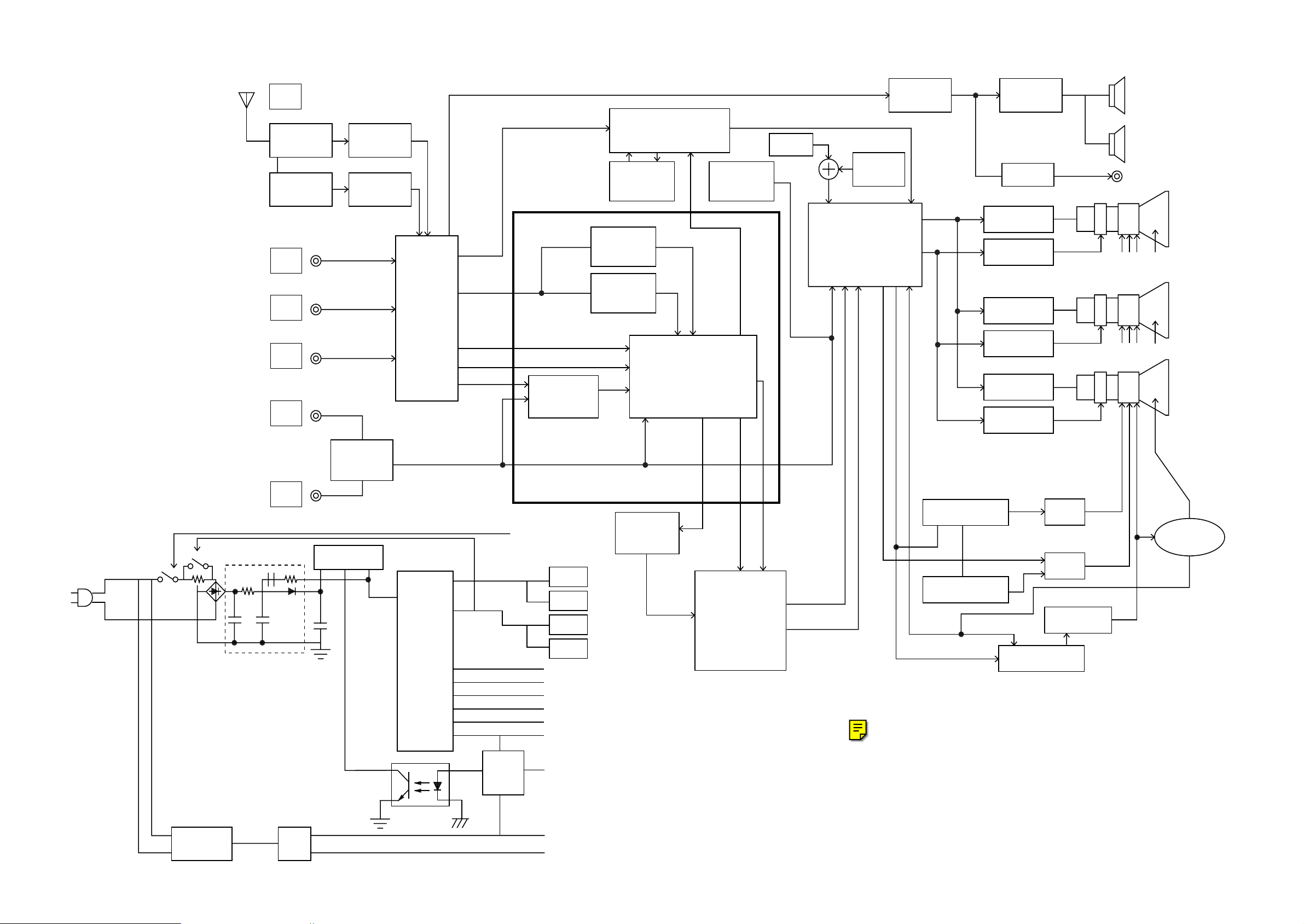
ANT
TUNER
with
antenna
SUB
TUNER
E1
E2
E3
C2
IF MPX
Module
IF Module
SYNC-AV
AV Switch
CXA2069Q
V-OUT
V-OUT
C-OUT
V-OUT2
CIRCUIT BLOCK DIAGRAM
Micro Processor
EEP ROM
3D YCS
TC90A65F
3L Comb
Filter
TDA9181T
YCYC
Multi Color Decoder
Y
C
Multi
Window
SDA9589X
RGB
Y Cb Cr
Y Cb Cr
CLK,DATA,CS,BUSY,RST
TEXT
Front End
Processor
TA1318N
HD
VD
D.CONV
RGB
RGB
RGB Processor
TA1360AN
HD
VD
SCP
Y Cb Cr YUV
SYNC
H
VP
Audio
Processor
RGB
AFC
AUDIO AMP
AMP
VIDEO OUT
SVM
VIDEO OUT
SVM
VIDEO OUT
SVM
SPEAKERS
HEADPHONE JACK
CRT
R
CRT
G
CRT
B
SR80
R820,
R821
SR81
D803
Higher harmonic circuit
C4
Y/Cb/Cr
SW
Q801
STR-Z4479
+
T862
TPW3516AS
E7
E11
E16
E-16
E32
E-32
E41
E120
AMP
POWER
Z801
Q831
5V-2
Q832
5V-3
Q830
9V-1
Q836
9V-2
DEF/CONV
DEF/CONV
DEF/CONV
DEF/CONV
AUDIO
DEF
X-REY
Picture
Improver
TDA9178T
Y Cb Cr
Noise
UP Converter
HD/VD
Q302
E/W
CORRECTION
Q460
DPC OUT
AFC
D CONVER
Q301
V OUT
Q404
H OUT
Q750,Q751,Q753
CONVER OUT
FBT
AFC
T860
SUB POWER
Q862
Q861TPW3517AH
E5-1
RESET
– 75 – – 76 –
Page 3
43VS9UA/UE/UT
50VS9UA/UE/UT
SIGNAL(OTHERS)
[SHEET-1/9]
Page 4
5.2
5.2 5.2 4.1
5.2
5.2
5.2
0
0
3.9
4.1
4.1
0
9.0
4.1
5.2
4.1
9.0
4.1
0
5.2
5.2
5.2
0
4.0
3.3
4.0
3.3
0
0
0
0
9
4.3
3.6
0
0
9
4.0
3.3
4.0
3.3
4.1
0
4.5
4.5
0
9.0
0
0
9.0
0
0
0
0
0
0
43VS9UA/UE/UT
50VS9UA/UE/UT
SIGNAL(AV)
[SHEET-2/9]
Page 5
12.0
36.0
190.70.71.0 0 191.0 19 000
9.0
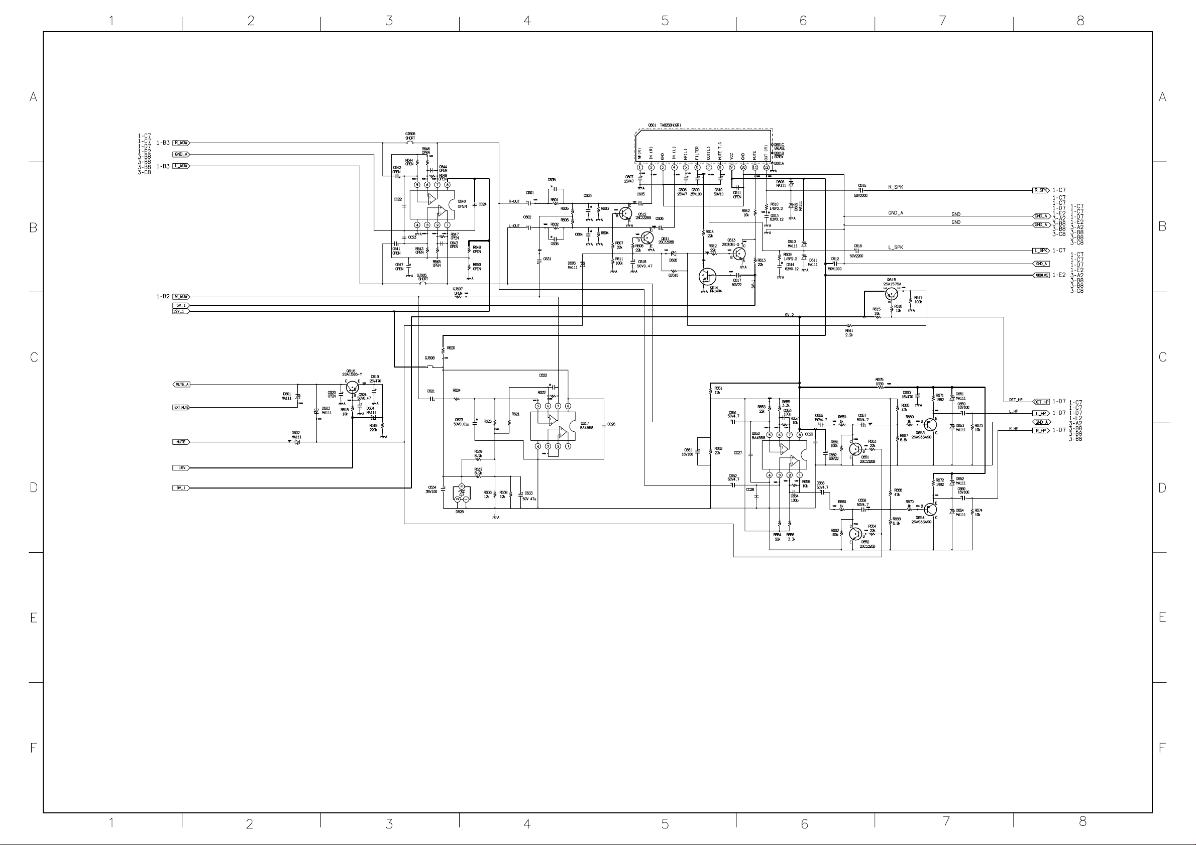
43VS9UA/UE/UT
50VS9UA/UE/UT
SIGNAL(SOUND)
[SHEET-3/9]
Page 6
4.24.2 32.05.0 9.0 0 0
5.0 32.0
04.3 4.3
9.000
4.2 4.2
5.0 32.0 0 9.0 5.0 4.2
4.2
0
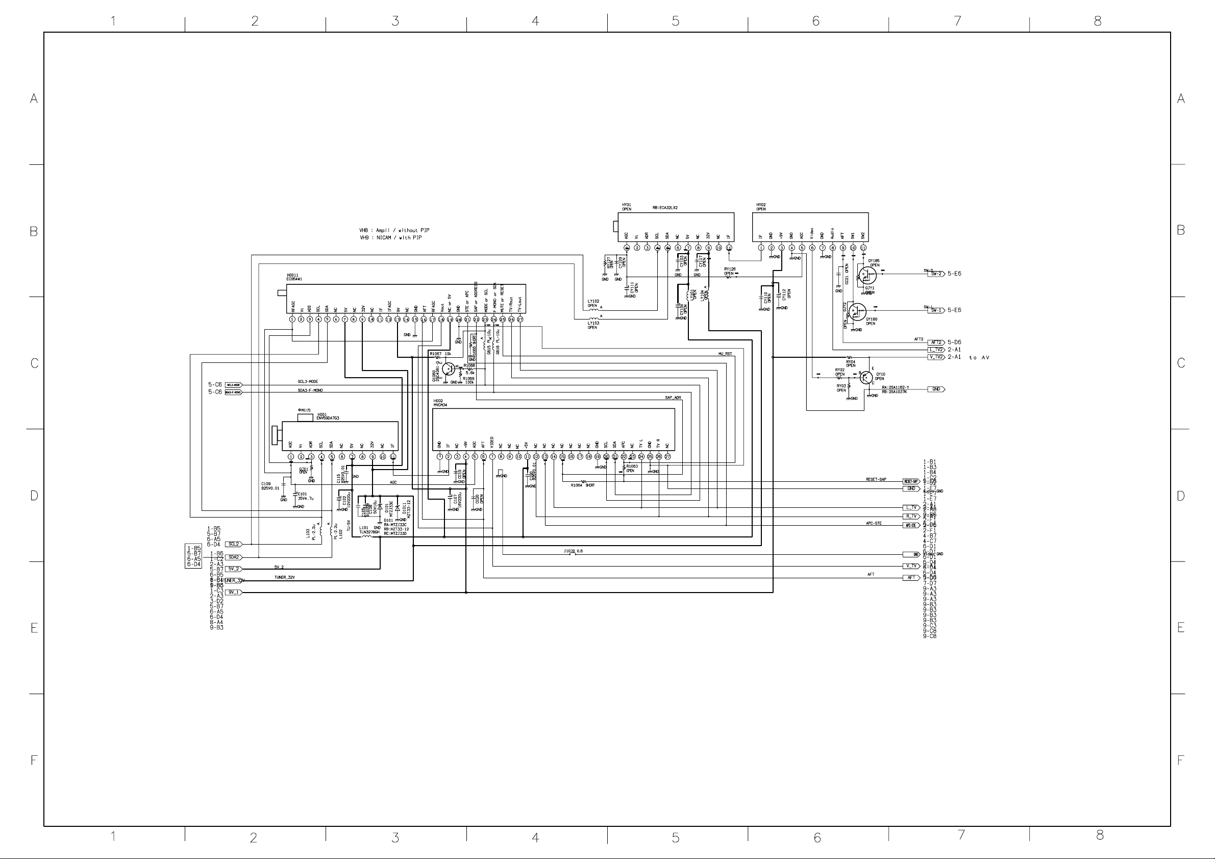
43VS9UA/UE/UT
50VS9UA/UE/UT
SIGNAL(IF)
[SHEET-4/9]
Page 7
5Vp-p
SCL
5Vp-p
SCL
5.0
0
4.5
4.5
4.5
4.5
5.0
0
0
2.0
4.5
4.5
5Vp-p
SDA
5.0
4.3
5.0
4.5
4.5
5.0
5.0
4.5
4.5
0
5Vp-p
SDA
4.2
4.2
5.0
5.0
4.7
4.5
4.5
fV
5Vp-p
fH
5Vp-p
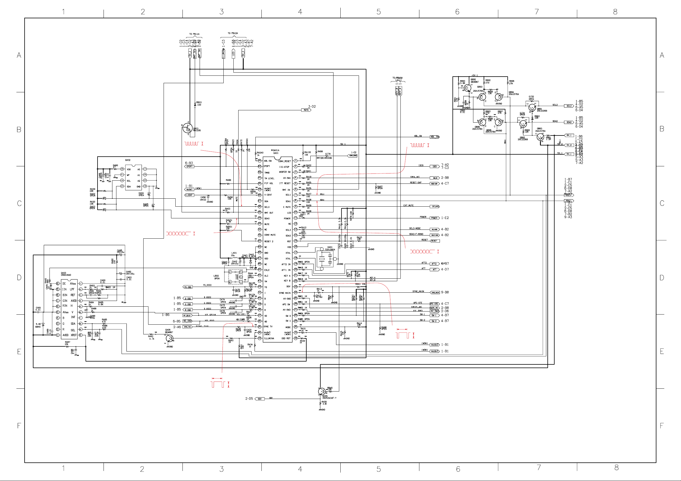
43VS9UA/UE/UT
50VS9UA/UE/UT
SIGNAL(M-CON)
[SHEET-5/9]
Page 8

10V/div
5ms/div
9.6V
2V/div 8V
5ms/div
16.6ms
GND
19.0
16.0 0.8 16.00.9 2.0
-16.0
58V
25V
7V
GND
16.6ms
75V
10V/div
55V
5ms/div
GND
0
9.0
0
4.5
4.5
0
43VS9UA/UE/UT
50VS9UA/UE/UT
SIGNAL(FEP/V-OUT OTHER)
[SHEET-6/9]
Page 9

0
4.5
5.0
5.0
4.54.5 4.5
0
5.0
0
43VS9UA/UE/UT
50VS9UA/UE/UT
SIGNAL(D-CONV)
[SHEET-7/9]
Page 10

ANT-GND
43VS9UA/UE/UT
50VS9UA/UE/UT
SIGNAL(REGU-OUT)
[SHEET-8/9]
Page 11

43VS9UA/UE/UT
50VS9UA/UE/UT
SIGNAL(3DYCS/OTHER)
[SHEET-9/9]
Page 12

43VS9UA/UE/UT
50VS9UA/UE/UT
DEF/CONV.(1/3)
[SHEET-1/3]
Page 13

15.0
0
9.0 8.27.4
126
-17.6
11.9
0
8.5 8.5 8.0 0
08.5 8.08.5
9.0
7.4
-17.6
8.2
43VS9UA/UE/UT
50VS9UA/UE/UT
DEF/CONV.(2/3)
[SHEET-2/3]
Page 14

0
0
0
-32.0
32.0
-16.0 -16.0-16.0
0 -16.032.0
-32.0 -16.0
-16.0
5.0
-5.0
-5.0
5.0
43VS9UA/UE/UT
50VS9UA/UE/UT
DEF/CONV.(3/3)
[SHEET-3/3]
Page 15

0.9V(p-p) (H)
0.78V(p-p) (H)
3.5V(p-p) (H)
5.6
3.0 0
6.6
6.3 2.4
0 2.5 2.5
9.1 5.7
2.7 00
1.3
7.3
3.5
0
0
3.5
0.103.3
4.7
1.5
0.53V(p-p)
(H)
3.5
4.8
0
4.8
0.75V(p-p)
(H)
3.4V(p-p) (H)
3.6V(p-p) (H)
43VS9UA/UE/UT
50VS9UA/UE/UT
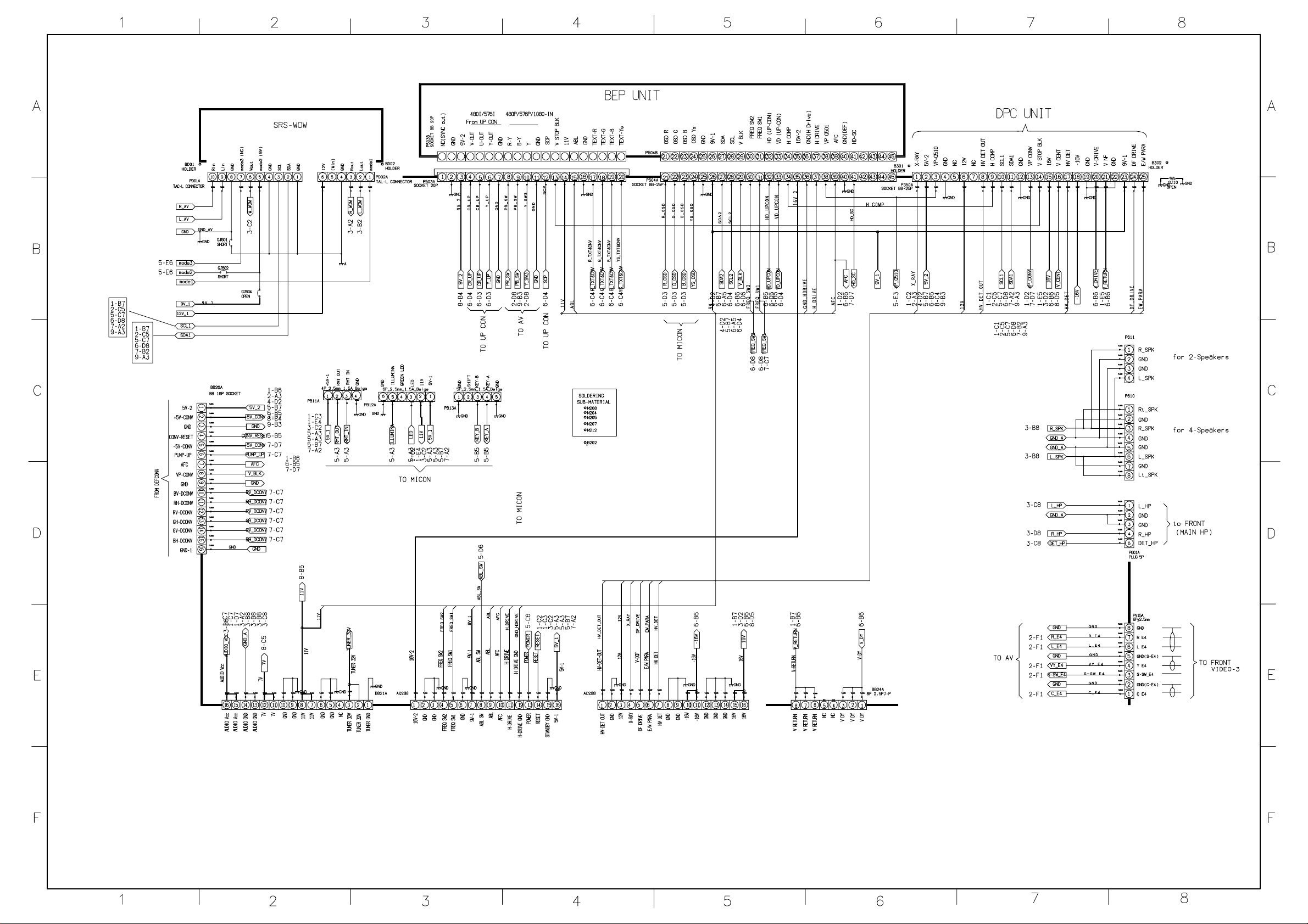
BEP
Page 16

1.2V(p-p)(V)
2.9
4.7
0
5.0
4.5
4.5
5.0
5.0
0
0 12.0
0
3.5V(p-p)(V)
3.1
3.4
0
4.5
4.5
3.2
0.8
9.4
5.5
0
3.4
1.1
16.0
0
9.0
-16.0
43VS9UA/UE/UT
50VS9UA/UE/UT
DPC
Page 17

1
156.7 2.30 6.1 5.8 5.9
3.6
7.70.3
0.8
0
85.4
17.8
78.3
2
119.0
6.000
125.3
124.9
5.4
120.7
0
119.7
0
2
1
1
2
50503
4
1
5µs
50V
2
5µs
50V
DC
5V5V10
DC
mV AC
mV AC
BWL5µs
10
1 AC 0V
Q801
14
1
0
T862
2
1
2
0
0
5.0
4.9
22.0
24.7
0
43VS9UA/UE/UT
50VS9UA/UE/UT
POWER
Page 18

220V
110V
0V
167.0
9.5
9.2
8.3
2.6
2.1
1H
148
9.5
9.2
8.0
2.9
2.3
220V
50V
0V
1H
220V
10V
0V
114
9.3
8.9
8.6
3.2
2.7
1H
43VS9UA/UE/UT
50VS9UA/UE/UT
CRT-D(for HD)/SVM(1/2)
[SHEET-1/2]
Page 19

10.6
6.1
5.4
10.6
5.4
5.1
119.1
119.3
61.9
8.9
1.5
0.8
10.6
6.0
5.4
6.0
0.8
0.1
10.6
6.1
5.4
10.6
5.4
5.1
119.1
119.3
61.9
61.9
5.0
4.8
0
10.6
6.1
5.4
10.6
5.4
5.1
0.8
0.5
119.3
119.1
61.9
5.0
4.8
0
61.9
0.8
0.5
61.9
5.0
4.8
0
0.8
0.5
43VS9UA/UE/UT
50VS9UA/UE/UT
CRT-D(for HD)/SVM(2/2)
[SHEET-2/2]
Page 20

6.0
6.0
6.0
6.0
6.0 6.0
6.0
6.0
6.0
6.0
6.0
0
6.0
6.0
0
0
0
0
0
3.9
3.9
12.0
0
6.0
6.0
12.0
6.0
6.0
6.0
6.0
6.0
6.0
6.0
6.0
6.0
0
6.0
6.0
0
0
6.0
6.0
6.0
6.0
6.0
0
0
6.0
6.0
0
5.1
0
43VS9UA/UE/UT
50VS9UA/UE/UT
SRS-WOW
Page 21

43VS9UA/UE/UT
50VS9UA/UE/UT
FRONT-IN RMT-IN
Page 22

43VS9UA/UE/UT
50VS9UA/UE/UT
M-TEXT-P2
 Loading...