

Page 1
SCHEMATIC DIAGRAM
MODEL : 43VJ22P
WARNING: BEFORE SERVICING THIS CHASSIS, READ THE "X-RAY RADIATION PRECAUTION", "SAFETY
PRECAUTION" AND "PRODUCT SAFETY NOTICE" ON THE MANUAL FOR THIS MODEL.
CAUTION: The international hazard symbols "*" in the schematic diagram and the parts list designate components
which have special characteristics important for safety and should be replaced only with types identical to those in the
original circuit or specified in the parts list. The mounting position of replacements is to be identical with originals.
Before replacing any of these components, read carefully the PRODUCT SAFETY NOTICE on the MANUAL for this
model. Do not degrade the safety of the receiver through improper servicing.
NOTE:
1. RESISTOR Resistance is shown in ohm [K = 1.000, M = 1.000.000]. All resistors are 1/6W and 5%
tolerance carbon resistor, unless otherwise noted as the following marks.
1/2R = Metal or Metal oxide of 1/2 watt 1/2S = Carbon compsistion of 1/2 watt
1RF = Fuse resistor of 1 watt 10W = Cement of 10 watt
K = ±10% G = ±2% F = ±1%
2. CAPACITOR Unless otherwise noted in schematic, all capacitor values less than 1 are expressed in
?F, and the values more than 1 in pF.
All capacitors are ceramic 50V, unless otherwise noted as the following marks.
Electolytic capacitor Mylar capacitor
3. The parts indicated with " * " have special characteristics, and should be replaced with identical parts only.
4. Voltages read with DIGITAL MULTI-METER from point indicated to chassing ground, using a color bar signal with all
controls at normal, line voltage 220 volts.
5. Waveforms are taken receiving color bar signal with enough sensitivity.
6. Voltage reading shown are nominal values and may vary ±20% except H.V.
SCHEMATIC DIAGRAM STRUCTURE:
SIGNAL Circuit ( MAICON / OTHER ) [ SHEET - 1/4 ] ................. 1/8
POWER Circuit ......................................................................................................... 5/8
DEF / CONV Circuit ( DEF ) [ SHEET - 1/2 ] ................. 6/8
CRT-D / SVM / FRONT Circuit ................................................................................. 8/8
( VCD / IF / V.OUT ) [ SHEET - 2/4 ] ................. 2/8
( AV / AUDIO ) [ SHEET - 3/4 ] ................. 3/8
( D-CONVER ) [ SHEET - 4/4 ] ................. 4/8
( CONV ) [ SHEET - 2/2 ] ................. 7/8
– 51 –
Page 2
RearCenter
Main
CRT.RCRT.GCRT.B
Q
Q
Q
Q
VIDEO OUT
SVM OUT
VIDEO OUT
SVM OUT
VIDEO OUT
SVM OUT
Q
Q
V OUT
Q301
H OUT
Q404
CONVER OUT
Q751,Q752
DY
DY
DY
SVMSVMSVM
D CONV ER
RGBYs
Q
Rear AMP
Q
Center AMP
Q
Main AMP
BACK END PROCESSOR
Q510
RGB
YM
OSD
QR01
RGB
RGB
MIXER
E/W
CORRECTION
VP
H
UP C ONVERTER
BLK/CP/B-MASK
YCbCr->YUV
Y2/U/Vin
Q302
FBT
AFC
AMP
Y
U
V
ADC
MPX
ADC
TC90A61F
DFS
VD
PLL
PLL
HD
EM626327Q
SGRAM
TIF
MAA
H001
H002
L,R,SL,SR,C
L,R
C
SL,SR
W
L,R OUT-1
TV-L,R
TV-V
ANT
DIGITAL
AUDIO IN
W-OUT
AMP
W
AV S WQV01
E1
E2
E3
I/O1
I/O2
I/O3
#8
#8
#8
TV-L, R out
V,L ,R O UT -2
AUDIO OUT
FIX
RGBYs
Y/V,C,L,R
S1
V1
V,L ,R
V,L ,R
S2
FRONT
S+AV
MICRO&TEXT
PROCESSOR
QA01
EEP-ROM
QA02
RGB Ys
SDA,SCL
SYNC-AV
SYNC-OUT
RGB
MULTI COLOR DECODER
Q501
EPG SW
CVBSout
Y1 in
Yviout
SYNCin
YCbCr
HD/VD
RGB1in
E4(YCbCr)
YCbCr1in
CVBS/Y2in
C-OUT C1in
D-COMB
Y-OUT
CVBS/Y1in
COMBin
Q
2001 Euro PJTV CIRCUIT BLOCK DIAGRAM
SPECIFIC INFORMATIONS
CIRCUIT BLOCK DIAGRAM
– 52 –
Page 3
5.0
0
0
0
0
0
4.5
4.5
4.5
4.5
5.0
0
0
0
0
0
5.0
0
5.0
0
0
0
0
0
0
0
5.0
0
5.0
5.0
4.5
4.5
4.5
4.5
0
5.0
43VJ22P
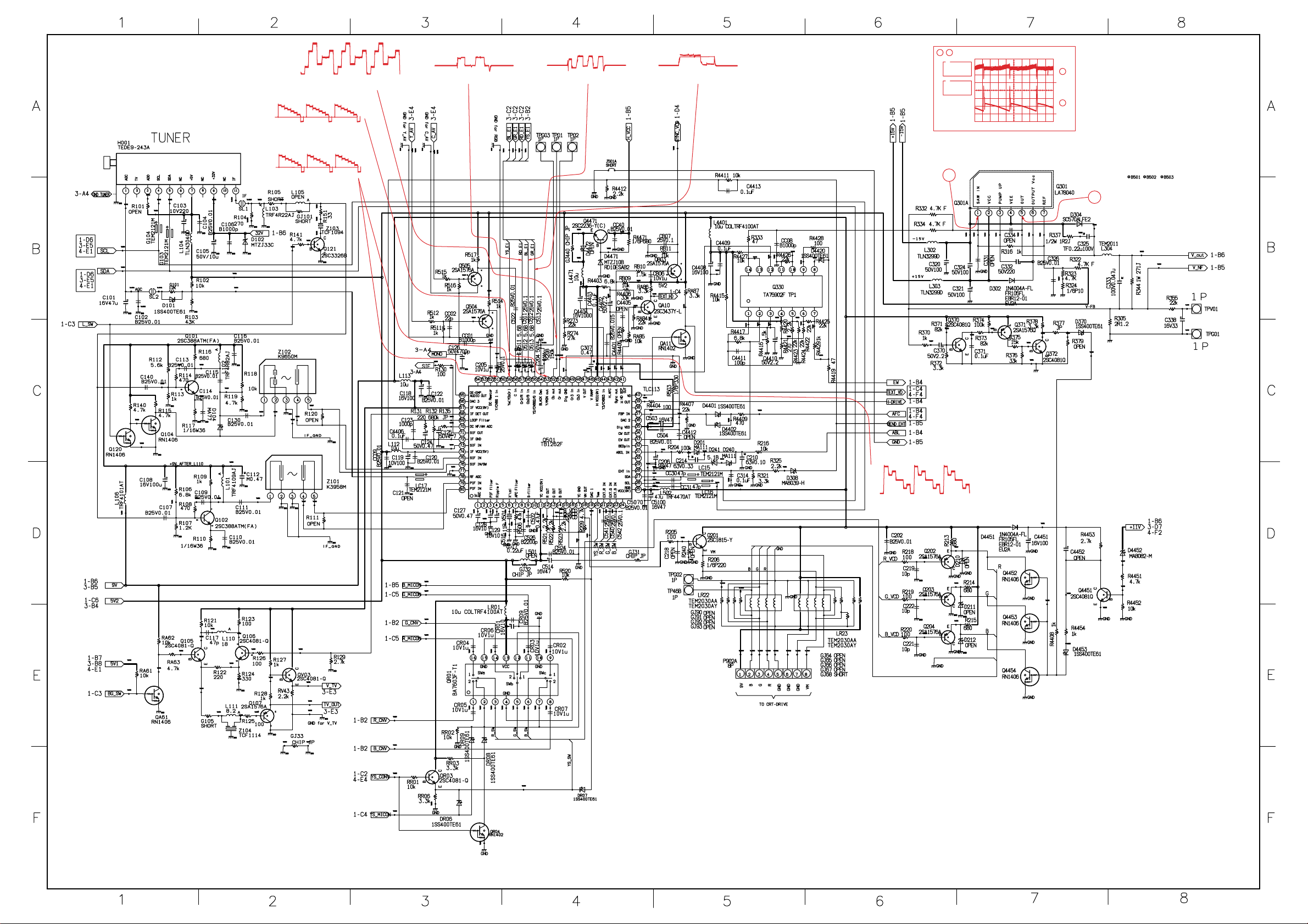
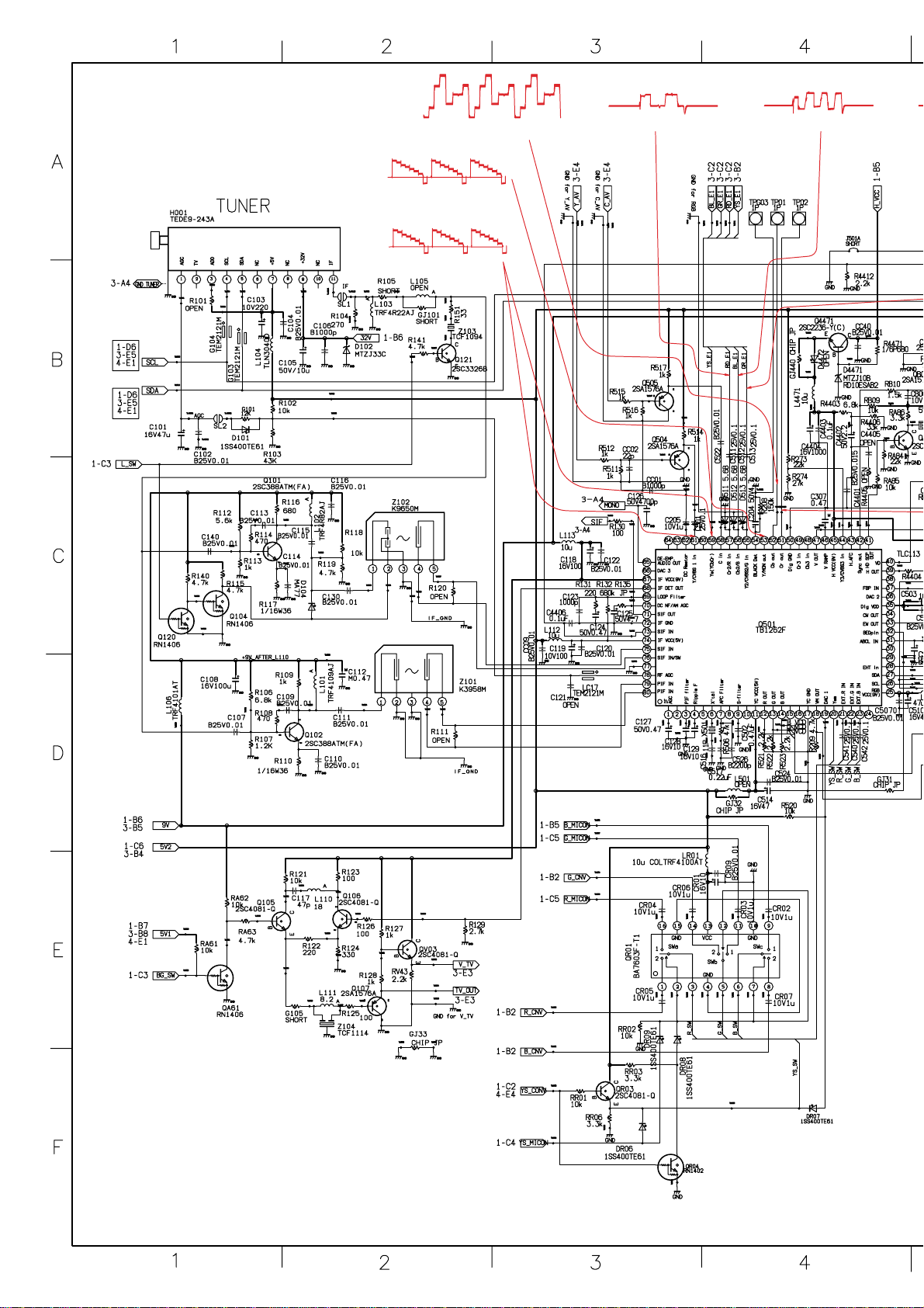
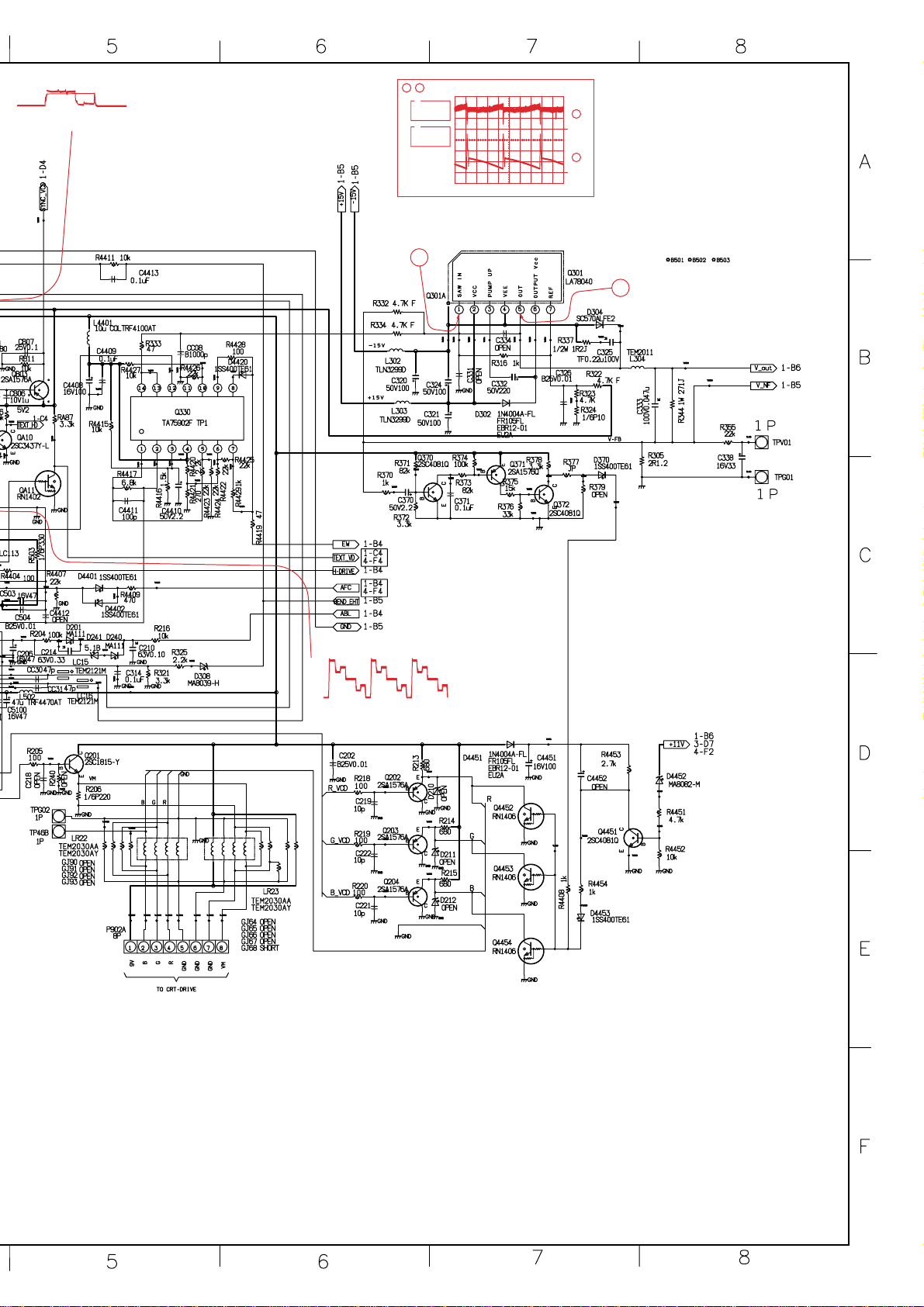
SIGNAL-MAICON/OTHER
[SHEET-1/4]
Page 4
5.0
0
0
0
0
0
4.5
4.5
4.5
4.5
5.0
0
0
0
0
0
5.0
0
5.0
0
0
5.0
0
0
5.0
5.0
4.5
4.5
4.5
4.5
0
0
0
0
0
5.0
Page 5
43VJ22P
SIGNAL-MAICON/OTHER
[SHEET-1/4]
Page 6
2
1
(H)
0.8V(p-p)
(H)
(H)
0.6V(p-p)
(H)
0.7V(p-p)
(H)
0.53V(p-p)
(H)
0.75V(p-p)
(H)
0.9V(p-p)
0.78V(p-p)
Q301
in
1
0
0
out
5
1
2
1
1
5ms/DIV.
2
0.5V/DIV.
5ms/DIV.
20V/DIV.
0
9.0
9.0
-15.0
15.0
5.0
32.0
4.1
4.1
2.4
3.5
3.5
3.5
9.0
2.3
0
4.5
5.0
4.5
0
9.0
3.0
2.4
2.4
0.8V(p-p)
221
1
0.5V/DIV.
2
5ms/DIV.
5ms/DIV.
20V/DIV.
(H)
0.53V(p-p)
(H)
(H)
0.7V(p-p)
(H)
0.75V(p-p)
0.78V(p-p)
(H)
Q301
1
in
1
0
5
out
2
0
(H)
0.9V(p-p)
5.0
4.1
4.1
32.0
0
2.4
3.0
9.0
0
2.4
3.5
3.5
2.4
3.5
2.3
5.0
9.0
9.0
4.5
4.5
9.0
0
0.6V(p-p)
1
15.0
-15.0
(H)
2
43VJ22P
SIGNAL-VCD/IF/V.OUT
[SHEET-2/4]
Page 7
(H)
0.8V(p-p)
(H)
(H)
0.7V(p-p)
0.7V(p-p)
(H)
0.75V(p-p)
(H)
0.9V(p-p)
0.78V(p-p)
0
9.0
9.0
5.0
32.0
4.1
4.1
2.4
3.5
3.5
3.5
9.0
2.3
0
4.5
5.0
4.5
0
9.0
3.0
2.4
2.4
(H)
(H)
0.75V(p-p)
0.78V(p-p)
(H)
0.8V(p-p)
(H)
(H)
0.9V(p-p)
5.0
4.1
4.1
32.0
2.4
3.5
3.0
3.5
3.5
9.0
0
2.4
2.3
0
9.0
2.4
9.0
4.5
4.5
9.0
0
5.0
Page 8
2
1
(H)
0.6V(p-p)
(H)
0.53V(p-p)
0.53V(p-p)
Q301
in
1
0
0
out
5
1
2
1
1
5ms/DIV.
2
0.5V/DIV.
5ms/DIV.
20V/DIV.
-15.0
15.0
221
1
5ms/DIV.
(H)
0.5V/DIV.
2
5ms/DIV.
20V/DIV.
Q301
1
in
1
0
5
out
2
0
1
0.6V(p-p)
15.0
-15.0
(H)
2
43VJ22P
SIGNAL-VCD/IF/V.OUT
[SHEET-2/4]
Page 9

0
9.000
0
5.0
5.0
0
13.0
30.0
8.8
12.9
1.9
1.9
1.9
1.9
4.5
4.5
4.1
4.1
8.3
2.1
6.9
4.1
0
9.0
4.1
5.2
5.2
5.2
5.2
5.2
0
6.6
4.1
4.1
3.9
4.1
5.2
5.2
5.2
5.2
5.2
5.2
5.2
0
5.2
0
0
9.0
0
1.9
1.9
1.9
001.9
0030.0
8.8
12.9
000013.0
8.3
2.1
6.9
0
5.2
5.2
5.2
6.6
0
5.2
5.2
5.2
5.2
5.2
5.2
5.2
5.2
5.2
4.5
4.5
4.1
4.1
5.2
0
4.1
4.1
9.0
4.1
4.1
4.1
3.9
43VJ22P
SIGNAL-AV/AUDIO
[SHEET-3/4]
Page 10

4.5
4.5
4.1
4.1
8.3
8.3
2.1
6.9
4.1
0
9.0
4.1
5.2
5.2
5.2
5.2
5.2
0
6.6
4.1
4.1
3.9
4.1
5.2
5.2
5.2
5.2
5.2
5.2
5.2
0
5.2
4.5
4.5
2.1
6.9
0
5.2
5.2
5.2
6.6
0
5.2
5.2
5.2
5.2
5.2
5.2
5.2
5.2
5.2
4.1
4.1
5.2
0
4.1
4.1
9.0
4.1
4.1
4.1
3.9
Page 11

0
9.000
0
5.0
5.0
0
13.0
30.0
8.8
12.9
1.9
1.9
1.9
1.9
0
0
9.0
0
1.9
1.9
1.9
001.9
0030.0
8.8
12.9
000013.0
43VJ22P
SIGNAL-AV/AUDIO
[SHEET-3/4]
Page 12

43VJ22P
SIGNAL-D-CONVER
[SHEET-4/4]
Page 13

Page 14

43VJ22P
SIGNAL-D-CONVER
[SHEET-4/4]
Page 15

ANT-GND
4
14
Q801
0
5
T862
1
2
22
1
2
50V
50V
s
s
10
10
DC
DC
AC
AC
1 AC 0V
5
5
1
2
50
50
V
mV
mV
V
BWL
2
1
5.4
0
119.7
120.7
85.4
78.3
0
0.8
17.8
3.6
0.3
5.9
5.8
2.3
0
156.7
7.7
TO SIGNAL
1
156.7
5.9
3.6
5.8
0
2.3
0.3
17.8
0.8
0
7.7
78.3
85.4
2
5.4
0
120.7
119.7
232322
1
55µµ s
50V
2
55µµ s
50V
55µµ s sBWL
10
DC
5
1
V
10
DC
5
2
V
AC
3350
mV
AC
4450
mV
1 AC 0V
Q801
14
1
0
T862
4
5
2
43VJ22P
POWER
Page 16

ANT-GND
4
14
Q801
0
5
T862
1
2
22
1
2
50V
50V
s
s
10
10
DC
DC
AC
AC
1 AC 0V
5
5
1
2
50
50
V
mV
mV
V
BWL
2
1
5.4
0
119.7
120.7
85.4
78.3
0
0.8
17.8
3.6
0.3
5.9
5.8
2.3
0
156.7
7.7
156.7
1
5.9
3.6
5.8
0
2.3
0.3
17.8
0.8
0
7.7
78.3
85.4
2
5.4
0
120.7
119.7
232322
1
55µµ s
50V
2
55µµ s
50V
55µµ s sBWL
10
DC
5
1
V
10
DC
5
2
V
AC
3350
mV
AC
4450
mV
1 AC 0V
Q801
14
1
0
T862
4
5
2
Page 17

TO SIGNAL
43VJ22P
POWER
Page 18

1
0
P414
1
5
200V/DIV.
5ms/DIV.
5
1
B
Q404
1
C
Q404
50V/DIV.
1
2
s/DIV.
3
1
500V/DIV.
s/DIV.
0
2
1
0
C
B
Q402
B
C
50V/DIV.
1
1
2
s/DIV.
0.5V/DIV.
s/DIV.
1
9
T461
Heater
1
s/DIV.
10V/DIV.
4
4
4
3
2
1
0
16.0
126
-17.6
-17.6
34.4
0
0.3
1
5050µµ s/DIV.
10V/DIV.
9
Heater
T461
1
4
16.0
0
2
126
-17.6
34.4
0.3
1
0
-17.6
3
5
2
1
2020µµ s/DIV.
50V/DIV.
3
1
2020µµ s/DIV.
500V/DIV.
1
1
2020µµ s/DIV.
0.5V/DIV.
2
2020µµ s/DIV.
50V/DIV.
B
C
Q402
B
1
0
C
2
0
B
Q404
C
Q404
5
1
5ms/DIV.
200V/DIV.
1
1
P414
43VJ22P
1
0
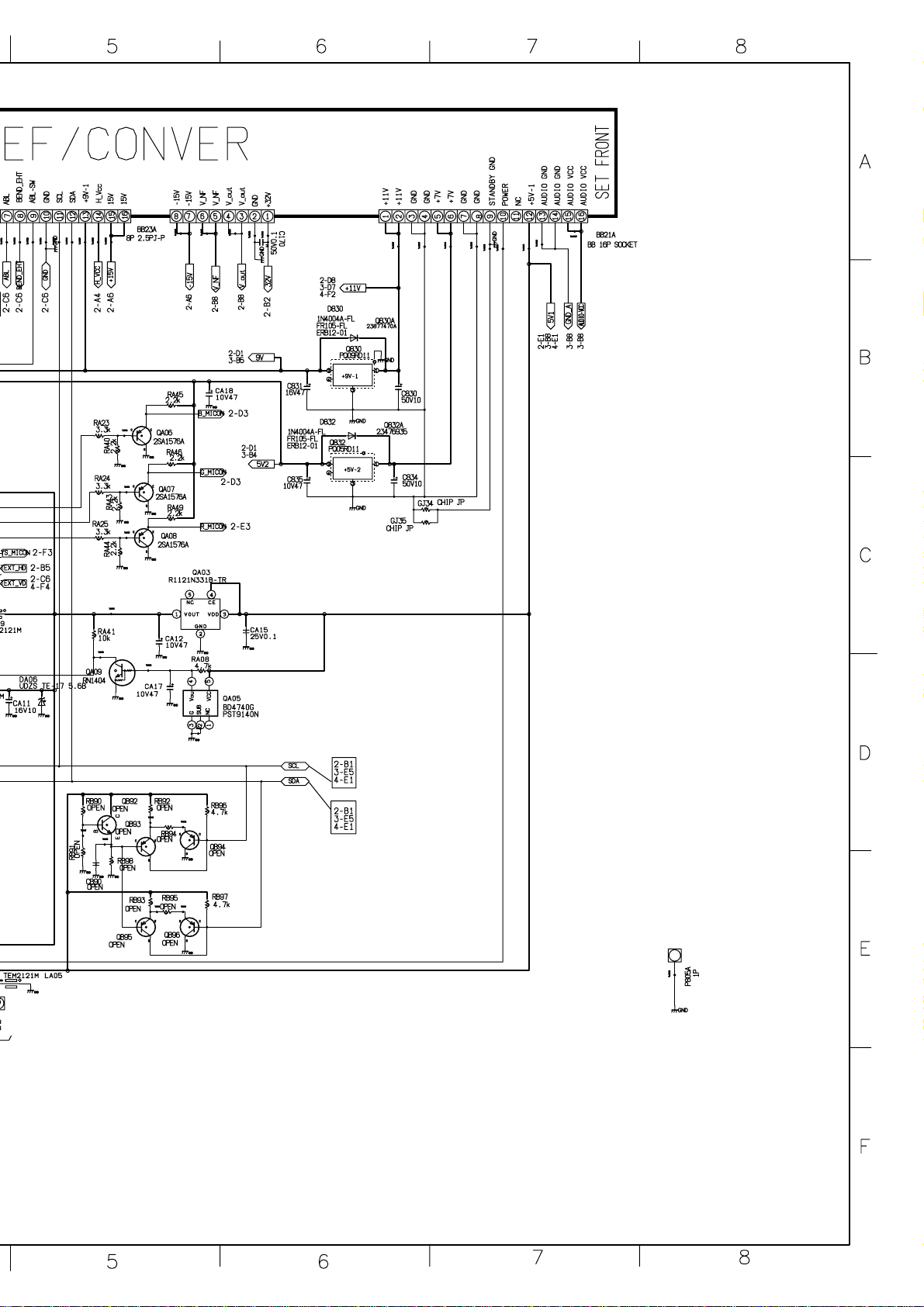
DEF/CONV(DEF)
[SHEET-1/2]
Page 19

9
4T461
Heater
1
s/DIV.
10V/DIV.
4
4
4
3
2
1
126
-17.6
-17.6
34.4
0
0.3
1
5050µµ s/DIV.
10V/DIV.
T
4
2
126
-17.6
-17.6
3
34.4
0.3
1
0
Page 20

1
0
P414
1
5
200V/DIV.
5ms/DIV.
5
1
B
Q404
1
C
Q404
50V/DIV.
1
2
s/DIV.
3
1
500V/DIV.
s/DIV.
0
2
1
0
C
B
Q402
B
C
50V/DIV.
1
1
2
s/DIV.
0.5V/DIV.
s/DIV.
1
9
T461
T461
Heater
0
16.0
9
Heater
1
16.0
0
5
2
1
2020µµ s/DIV.
50V/DIV.
1
1
2020µµ s/DIV.
0.5V/DIV.
B
2
2020µµ s/DIV.
50V/DIV.
C
Q402
1
2
3
1
2020µµ s/DIV.
500V/DIV.
B
0
C
0
Q404
Q404
B
C
5
1
5ms/DIV.
200V/DIV.
1
1
P414
1
0
43VJ22P
DEF/CONV(DEF)
[SHEET-1/2]
Page 21

-16
-1600
-16
0
16
-16
16.0
0
-16
-16
0
16
-16
16.0
-16
-9
5.0
0
0
5.0
-16
-16
0
-16
16
-16
16.0
16.0
0
5.0
0
5.0
16
99161600-16
00-16
0
-16
-16
16.0
16
99161600-16
0
-16
0
-16
-16
16.0
99161600-16
16
-16
0
-16
-16
0
0
5.0
5.0
5.0
-9-90
0
5.0
-9
43VJ22P
DEF/CONV(CONV)
[SHEET-2/2]
Page 22

16.0
-16
-16
0
-16
16
-16
16.0
16.0
0
5.0
0
5.0
16
99161600-16
00-16
0
-16
-16
16.0
0
0
5.0
5.0
Page 23

-16
-1600
-16
0
16
-16
16.0
0
-16
-16
0
1616-16
-16
-16
-9
5.0
0
0
5.0
99161600-16
0
0
-16
-16
16.0
99161600-16
-16
16
0
-16
-16
-9-90
0
5.0
5.0
-9
43VJ22P
DEF/CONV(CONV)
[SHEET-2/2]
Page 24

1H
220V
10V
0V
220V
50V
0V
1H
220V
220V
1H
110V
0V
6.1
10.6
10.6
5.4
6.0
119.3
61.9
119.1
0.8
61.9
0.5
5.4
10.6
5.1
5.4
4.8
5.0
0
0.8
6.0
0.1
8.9
0.8
1.5
114
9.3
8.9
8.6
2.7
3.2
9.2
9.5
148
8.
2.9
2.3
9.2
8.3
9.5
2.6
167.0
2.1
1.7
0
9.0
6.0
2.4
0
0
2.4
1.6
0
1.7
1.7
1.1
9.0
0.9
110V
0V
9.0
1.7
1.7
1.1
0
167.0
9.5
9.2
8.3
2.6
2.1
6.0
1.6
0.9
2.4
2.4
9.0
0
0
0
1H
1.7
148
9.5
9.2
8.
2.9
2.3
220V
50V
0V
1H
114
9.3
8.9
8.6
3.2
2.7
220V
10V
0V
1H
10.6
6.0
8.9
1.5
0.8
5.4
0.8
6.0
0.1
10.6
6.1
5.4
10.6
5.4
5.1
5.0
4.8
0
119.3
119.1
61.9
61.9
0.8
0.5
43VJ22P
CRT-D/SVM/FRONT
Page 25

220V
220V
1H
110V
0V
6.1
10.6
10.6
5.4
6.0
119.3
61.9
119.1
0.8
61.9
0.5
5.4
10.6
5.1
5.4
4.8
5.0
0
0.8
6.0
0.1
8.9
0.8
1.5
9.2
9.5
148
8.
2.9
2.3
9.2
8.3
9.5
2.6
167.0
2.1
1.7
0
9.0
6.0
2.4
0
0
2.4
1.6
0
1.7
1.7
1.1
9.0
0.9
110V
0V
1H
9.0
1.7
1.7
1.1
0
167.0
9.5
9.2
8.3
2.6
2.1
6.0
1.6
0.9
2.4
2.4
1.7
9.0
0
0
0
10.6
6.0
8.9
1.5
0.8
5.4
0.8
6.0
0.1
10.6
6.1
5.4
10.6
5.4
5.1
5.0
4.8
0
119.3
119.1
61.9
61.9
0.8
0.5
Page 26

1H
220V
220V
10V
0V
220V
50V
0V
1H
114
9.3
8.9
8.6
2.7
3.2
9.2
9.5
148
8.
2.9
2.3
10V
0V
220V
50V
0V
148
9.5
9.2
8.
2.9
2.3
1H
114
9.3
8.9
8.6
3.2
2.7
1H
43VJ22P
CRT-D/SVM/FRONT
 Loading...