

Page 1

FILE NO. 030-200403
SERVICE MANUAL
Colour Television
43VJ33Q
VJ13 Chassis
50VJ33Q
Published in Japan, May. 2004 (YC)
Page 2

TABLE OF CONTENTS
CHAPTER 1 GENERAL ADJUSTMENTS
SAFETY INSTRUCTIONS ........................................................................................................................................3
CRT ASSEMBLY REPLACEMENT AND MOUNTING .............................................................................................. 4
PICTURE TUBE COMPONENTS ADJUSTMENT.................................................................................................... 6
SERVICE POSITION ................................................................................................................................................ 9
SERVICE MODE .................................................................................................................................................... 10
DESIGN MODE ...................................................................................................................................................... 13
ELECTRICAL ADJUSTMENT................................................................................................................................. 14
CONVERGENCE ADJUSTMENT ........................................................................................................................... 19
SCREEN AND MIRROR ALIGNMENTS ................................................................................................................. 25
CIRCUIT CHECKS ................................................................................................................................................. 26
CHAPTER 2 SPECIFIC INFORMATIONS
SETTING & ADJUSTING DATA ............................................................................................................................. 27
LOCATION OF CONTROLS................................................................................................................................... 28
PROGRAMMING CHANNEL MEMORY................................................................................................................. 30
MECHANICAL DISASSEMBLY .............................................................................................................................. 31
CHASSIS AND CABINET REPLACEMENT PARTS LIST ......................................................................................32
PC BOARDS BOTTOM VIEW................................................................................................................................. 45
TERMINAL VIEW OF TRANSISTORS ................................................................................................................... 55
CIRCUIT BLOCK DIAGRAM .................................................................................................................................. 57
SPECIFICATIONS .............................................................................................................................................. END
APPENDIX:
CIRCUIT DIAGRAM
-
2
-
Page 3

CHAPTER 1 GENERAL ADJUSTMENTS
SAFETY INSTRUCTIONS
WARNING: BEFORE SERVICING THIS CHASSIS, READ THE “X-RAY RADIATION PRECAUTION”, “SAFETY PRECAU-
TION” AND “PRODUCT SAFETY NOTICE” INSTRUCTIONS BELOW.
X-RAY RADIATION PRECAUTION
1. Excessive high voltage can produce potentially hazardous X-RAY RADIATION. To avoid such hazards, the high
voltage must not be above the specified limit. The nominal
value of the high voltage of this receiver is (A) kV at zero
beam current (minimum brightness) under a (C) V AC power
source. The high voltage must not, under any circumstances, exceed (B) kV.
Refer to table-1 for high voltage (A), (B) & AC voltage (C).
(See SETTING & ADJUSTING DATA on page 26)
Each time a receiver requires servicing, the high voltage
should be checked following the HIGH VOLTAGE CHECK
procedure in this manual. It is recommended that the reading of the high voltage be recorded as a part of the service
record. It is important to use an accurate and reliable high
voltage meter.
SAFETY PRECAUTION
WARNING : Service should not be attempted by anyone unfamiliar with the necessary precautions on this receiver. The following
are the necessary precautions to be observed before servicing this chassis.
1. An isolation transformer should be connected in the power line between the receiver and the AC line before any service is
performed on the receiver.
2. Always discharge the picture tube anode to the CRT conductive coating before handling the picture tube. The picture tube
is highly evacuated and if broken, glass fragments will be violently expelled. Use shatter proof goggles and keep picture tube
away from the unprotected body while handling.
3. When replacing a chassis in the cabinet, always be certain that all the protective devices are put back in place, such as; nonmetallic control knobs, insulating covers, shields, isolation resistor-capacitor network etc.
2. The only source of X-RAY RADIATION in this TV receiver
is the picture tube. For continued X-RAY RADIATION protection, the replacement tube must be exactly the same
type tube as specified in the parts list.
3. Some part in this receiver have special safety-related characteristics for X-RAY RADIATION protection. For continued safety, parts replacement should be undertaken only
after referring to the PRODUCT SAFETY NOTICE below.
PRODUCT SAFETY NOTICE
Many electrical and mechanical parts in this chassis have special safety-related characteristics. These characteristics are
often passed unnoticed by a visual inspection and the protection afforded by them cannot necessarily be obtained by using
replacement components rated for higher voltage, wattage, etc. Replacement parts which have these special safety characteristics are identified in this manual and its supplements; electrical components having such features are identified by
the international hazard symbols on the schematic diagram and the parts list.
Before replacing any of these components, read the parts list in this manual carefully. The use of substitute replacement
parts which do not have the same safety characteristics as specified in the parts list may create shock, fire, X-ray
radiation or other hazards.
-
3
-
Page 4
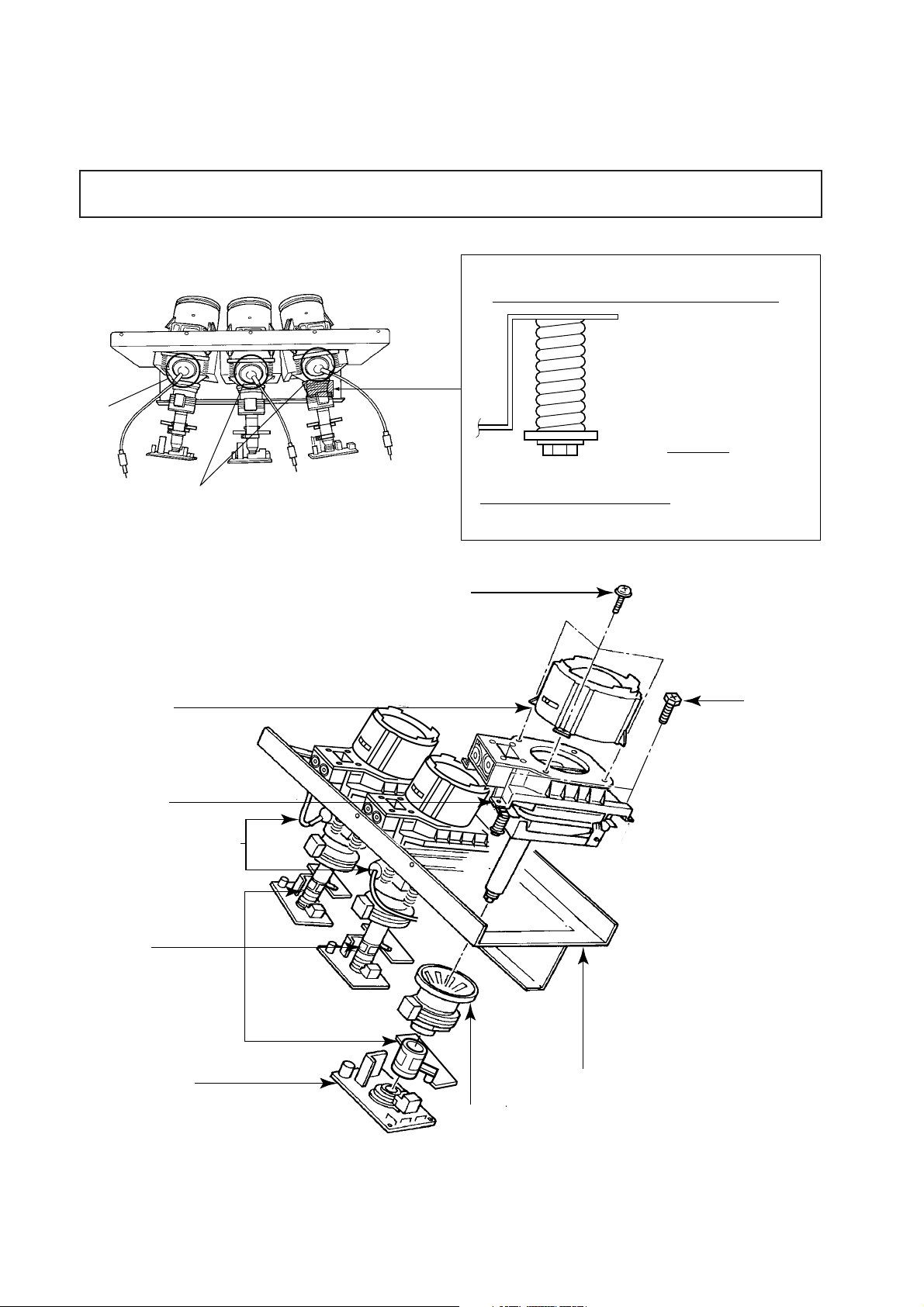
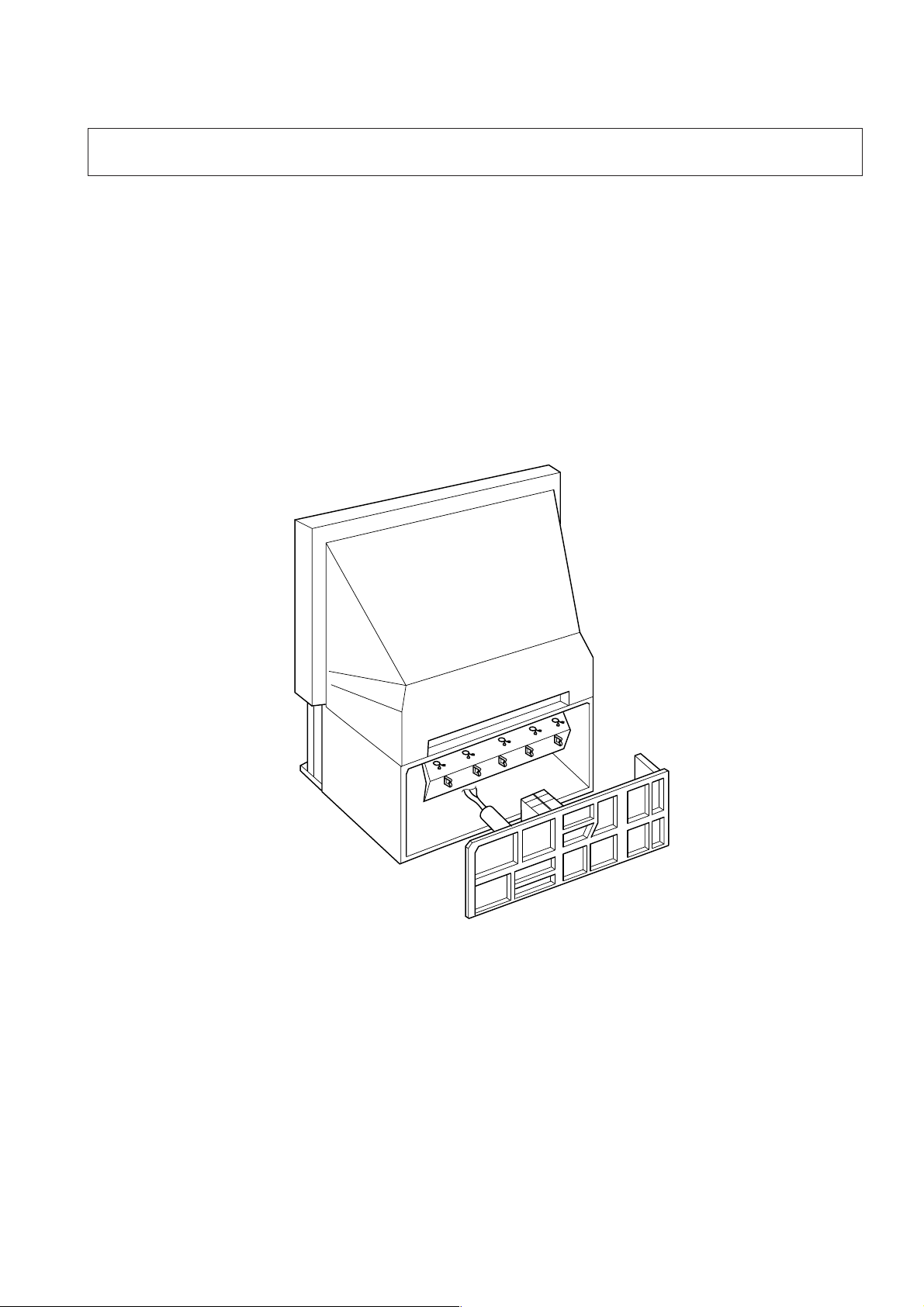
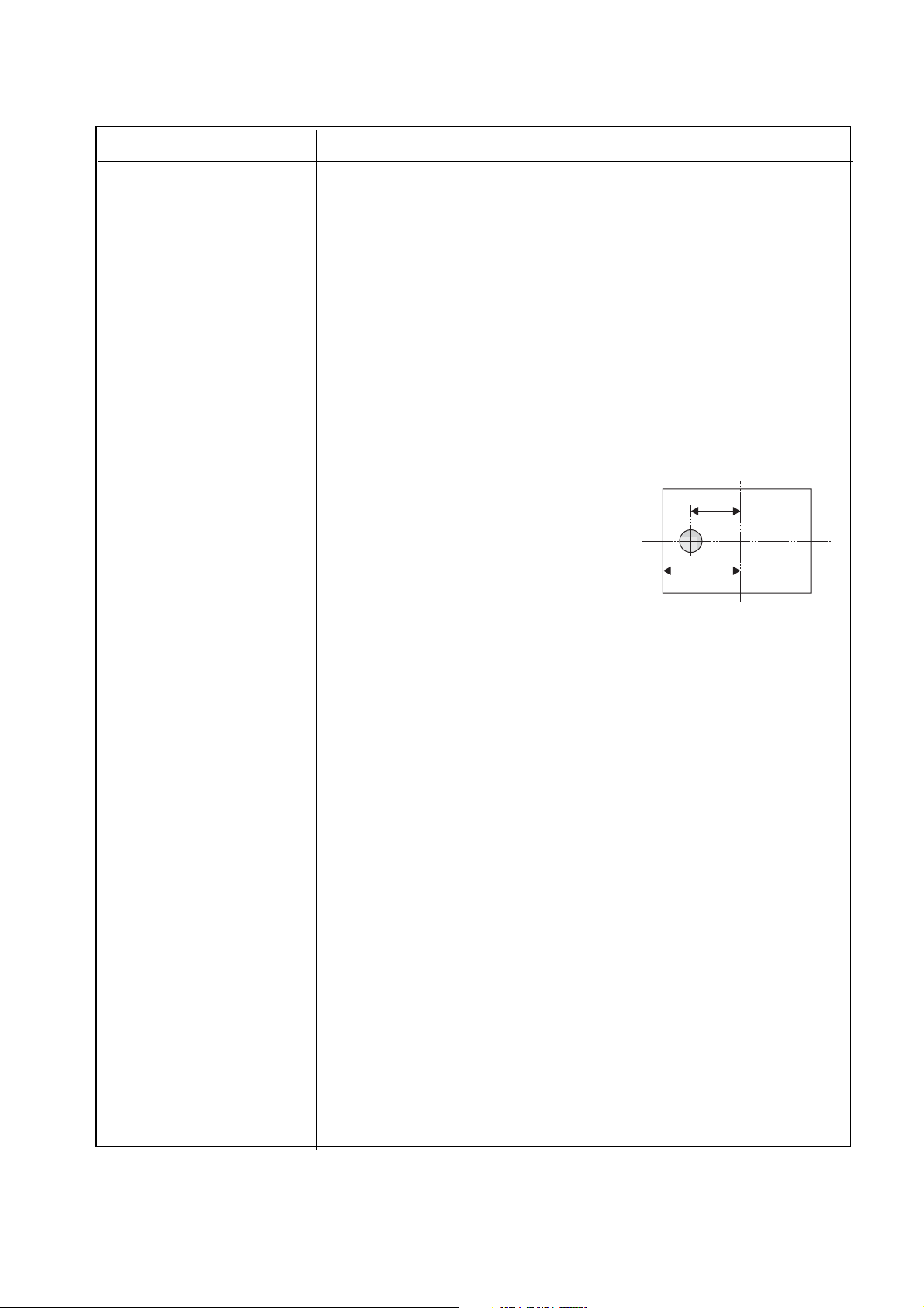
CRT ASSEMBLY REPLACEMENT AND MOUNTING
CAUTION : DO NOT LOOSEN THE HEX HEAD BOLTS WITH SPRINGS (12 PCS), BECAUSE THOSE ARE FOR
SEALING OF CRT COOLANT.
Attention Serviceman
The Hex Head
Bolts with
Springs. (see
sketch) used on
CRT assembly,
are “NOT”
Adjustment Screws
DO NOT LOOSEN-FLUID
LEAKAGE WILL OCCUR.
Lens Assembly
CRT Assembly
CRT Anode Cap Assembly
S.V.M. Coil
4 Screws
4 Screws
CRT DRIVE Board
Deflection Yoke and Conver Yoke
Lens and Neck Components View
-
4
-
CRT Mounting
Page 5
TO REMOVE CRT (Same procedure for R, G, B)
1. Remove CRT DRIVE Board, S. V. M. COIL and
DEF. YOKE from CRT.
2. Remove Lens Assembly.
3. Detach CRT Anode Cap from CRT.
4. Remove CRT Assembly from CRT Mounting.
CRT REPLACEMENT (Same procedure for R, G, B)
Reverse the removal procedures except the followings.
1. Anode Cable should be replaced with new one.
See "SERVICING PRECAUTIONS" shown below.
2. Install silicon (T461B) to the CRT, replace the Anode
cable and put enough silicon again on around the Anode Cap as illustrated.
CAUTION: Align the Anode cable as illustrated on page
4.
ADJUSTING PROCEDURE IN REPLACING CRT
1. R.G.B. CUTOFF (SCREEN VR) ADJUSTMENT (page 6.)
2. R.G.B. FOCUS ADJUSTMENT (page 6.)
3. PICTURE TILT ADJUSTMENT (page 7.)
4. USER CONVERGENCE CENTER CHECK
(Refer to owner's manual.)
5. CENTERING ADJUSTMENT (page 7.)
6. CONVERGENCE ADJUSTMENT (page 20.)
7. WHITE BALANCE ADJUSTMENT (page 14.)
Adjustments are complete.
Anode Cap
Silicon
(On shaded area)
TSE3843W #23960136
2 ~ 5 mm
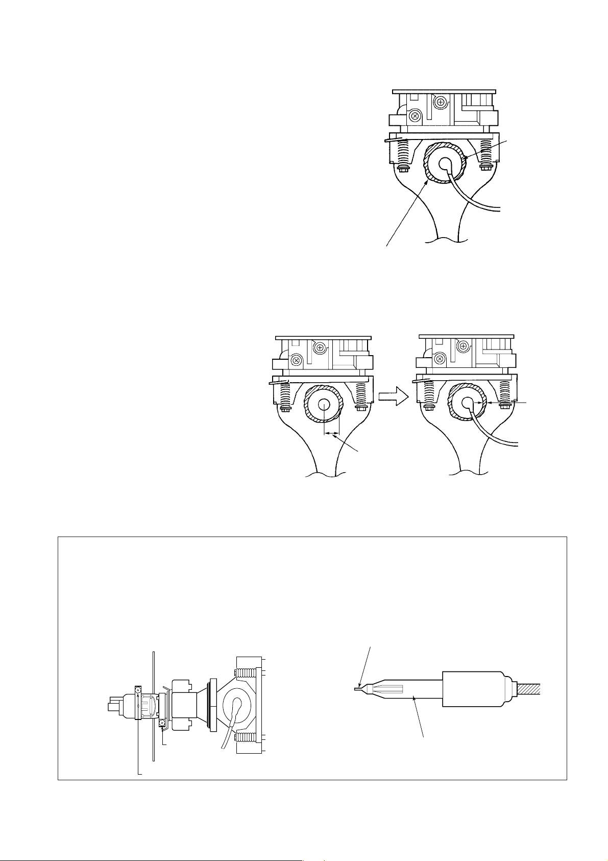
SERVICING PRECAUTIONS
■ Do not use a magnetized screw driver for screws
of Deflection Yoke and Velocity Modulation Coil to
avoid magnetization of electron gun.
Magnetization of electron gun will degrade basic
function and result in unbalance of right and left
shift of user static convergence, and result in no
variable quantity.
Screw
for D.Y
15 ~ 25 mm
■ When replacing the anode cap assembly (CRT) or
anode lead assembly (F.B.T.), remove the anode
lead holder from old one and attach the holder
again to new anode lead.
■ Check the point of anode lead in a straight
line, if it is winding, please revise it.
Anode lead holder
Screw for SVM coil
-
5
-
Page 6
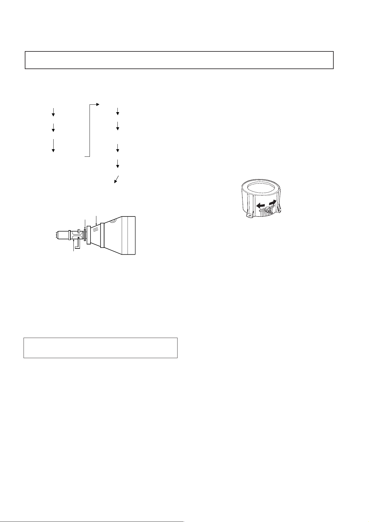
WARNING
CAUTION" AND "PRODUCT SAFETY NOTICE" ON PAGE 3 OF THIS MANUAL.
: BEFORE SERVICING THIS CHASSIS, READ THE "X-RAY RADIATION PRECAUTION", "SAFETY PRE-
PICTURE TUBE COMPONENTS ADJUSTMENT
ADJUSTING PROCEDURE IN REPLACING CRT
Cutoff
Lens focus
Electrical focus
Yoke horizontal
DESCRIPTION OF NECK COMPONENTS
2
S.V.M. COIL
1 Deflection yoke and convergence yoke.
The position on the neck is required most front (CRT funnel side) and the screw is fastened after rotating yoke
adjusting picture tilt.
2
Centering magnet
After adjusting picture tilt, picture position is finally fixed
by this magnet.
In order to get maximum margin of user convergence control for center of screen, this magnet have to be used for
center convergence adjustment.
User convergence center check
Centering (PAL)
Convergence adjustment
(PAL/NTSC)
White balance
Sub bright adjustment
End
1
RGB FOCUS ADJUSTMENT
1. Connect a VIDEO signal generator which generates a
cross-hatch pattern.
2. Receive a white cross-hatch pattern by pressing the signal
slection key on the VIDEO signal generator.
3. Expose only RED by covering the GREEN and BLUE
lenses with caps.
4. Loosen the RED lens fixing screws (refer to Fig. a), and
adjust the RED lens focus to obtain the sharpest point
while observing the middle and peripheral sections of the
screen.
Fig. a
5. Use the focus VR of “R” of the focus pack in order to adjust
the electric focus in the middle and peripheral sections of
the screen to its sharpest level.
6. Check the RED focus of the whole screen and if necessary
repeat steps 4 and 5.
7. Fix the RED lens by tightening its fixing screws.
8. Expose only GREEN by covering the RED and BLUE
lenses with caps.
9. Display the internally-generated cross-hatch signal.
10. Adjust the GREEN lens focus on the left border of the
screen to its sharpest level, then check the focus on the
right border, and if it is at its sharpest level, fix it in that
position by tightening the lens screws.
PREPARATION
Operate the receiver for at least 5 minutes.
R, G, B CUTOFF (SCREEN VR) ADJUSTMENT
1. Adjust before replace the screen assembly.
2. Set user control to reset position.
CONTRAST → Max
(
BRIGHTNESS, COLOR, TINT → Center.
3. Call up the adjustment mode display, then select the
item RCUT.
4. Adjust the data of items RCUT, GCUT, and BCUT to
"40H".
5. Press the -/-- button on Remote. (Y-MUTE : ON)
6. Gradually rotate R, G and B screen volume of FOCUS
PAC clockwise or counterclockwise until the raster
appears slightly on the CRT through the each lens, and
leave them.
(Lookin to the lens in order to check the raster.)
7. Press the -/-- button on Remote. (Return to Normal
Picture)
(1) If the horizontal line toward the right border is red-
flared, turn the lens screw slightly right in order to
balance it with the left border. (After adjustment, the
left border tends to be slightly green-flared, and the
right border tends to be slightly red-flared.)
(2) If the horizontal line toward the right border is green-
)
Note: The aim of the above-described adjustment procedure
-
6
flared, turn the lens screw slightly left in order to
balance it with the left border. (After adjustment, the
left border tends to be slightly red-flared, and the
right border tends to be slightly green-flared.)
for the Green lens focus is to obtain the best lens focus
after 2 - 3 hours of warming up taking into account the
focus drift; it applies if the warming up time before the
adjustment is less than 30 minutes. (The horizontal line
in the screen middle section tends to be slightly redflared.)
-
Page 7

In case of warming up of more than 2 hours under a condition
that the large anode current is running through the projection
tube so that for example the all-white pattern appears, adjust
to obtain the sharpest focus while observing the whole screen
like in the RED case.
11. Use the focus VR of “G” of the focus pack in order to adjust the electric focus in the middle section of the screen
to its sharpest level.
Note: Normally the most clearly visible point of the scanning
line is the sharpest point of the Green focus, however as
the characteristics vary depending on the projection tube,
the sharpest focus points of the vertical and horizontal
lines may not match each other, thus when you turn the
focus VR, if the picture tends to be tremendously unstable
(rolls horizontally or vertically), adjust the balance of the
vertical and horizontal lines to its best position.
TILT ADJUSTMENT
Rotate R, G, B deflection yoke so that picture becomes horizon, then fasten screw.
CENTERING ADJUSTMENT
1. Stretch threads towards the center of the screen (top and
bottom, left and right).
12. Check the GREEN focus of the whole screen and if
necessary repeat steps 10 and 11.
13. Fix the GREEN lens by tightening up its fixing screws.
14. Expose only BLUE by covering the RED and GREEN
lenses with caps.
15. Loosen the BLUE lens fixing screws (refer to Fig. a), and
adjust the BLUE lens focus while observing the middle
and peripheral screen sections.
16. Use the focus VR of “B” of the focus pack in order to adjust
the focus in the middle section of the screen to its sharpest
level.
(The point of the Blue focus becomes sharpest when the
brightness level of BLUE is lowest, the cross-hatch is
clearly visible.)
17. Check the BLUE focus of the whole screen and if necessary repeat steps 15 and 16.
18. Fix the BLUE lens by tightening its fixing screws.
2. Enter to the user's Convergence Adjustment Mode from
the menu.
3. Adjust G centering magnet so that the cross pattern center comes to screen center.
4. Perform HEIGHT adjustment . (See page 14.)
5. Perform VERT. LINEARITY adjustment. (See page 14.)
6. Perform WIDTH adjustment. (See page 14.)
7. Check whole quality of green line.
8. Adjust R, B centering magnet so that the cross pattern
center comes to screen center.
-
7
-
Page 8
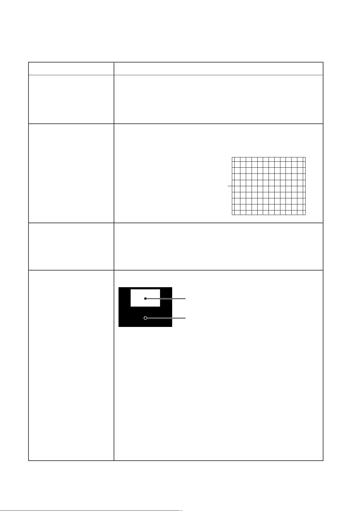
LOCATION OF SCREEN AND FOCUS VR'S
To remove the Speaker grille and Front panel.
Speaker grille
RGB
SCREEN VR's
FOCUS VR's
REPLACEMENT OF HIGH VOLTAGE CABLE
ANODE LEAD
RUBBER BOOT
LEAD HOLDER
Fig. a
Z450 TPA5007
1. When replacing Anode Lead or Anode Cap with new
one, remove Lead Holder from old lead as shown in
figure below, and put it on new lead. Do not throw away
Lead Holder.
NOTE : THE LEAD HOLDER IS ATTACHED TO
TPA5007 (Z450), BUT IS NOT ATTACHED TO
ANODE LEAD AND ANODE CAP. RUBBER
BOOT IS ATTACHED TO ANODE LEAD AND
ANODE CAP.
2. Detaching Lead Holder
OLD
ANODE LEAD
or
ANODE CAP
LOCK
RUBBER BOOT
LEAD HOLDER
Fig. b
Cut here rubber boot
and lead together to
detach Lead Holder.
-
8
-
Page 9
WARNING
CAUTION" AND "PRODUCT SAFETY NOTICE" ON PAGE 3 OF THIS MANUAL.
: BEFORE SERVICING THIS CHASSIS, READ THE "X-RAY RADIATION PRECAUTION", "SAFETY PRE-
SERVICE POSITION
In order to assure the performance, processed wires shall be replaced after the repair work.
Work procedures are as follows:
1. Remove the back board.
2. Remove lead wires.
3. Draw out the chassis.
4. Rest the chassis against the back cabinet, chassis as shown bellow.
After repair work finished, replace it in the opposite procedure.
-
9
-
Page 10
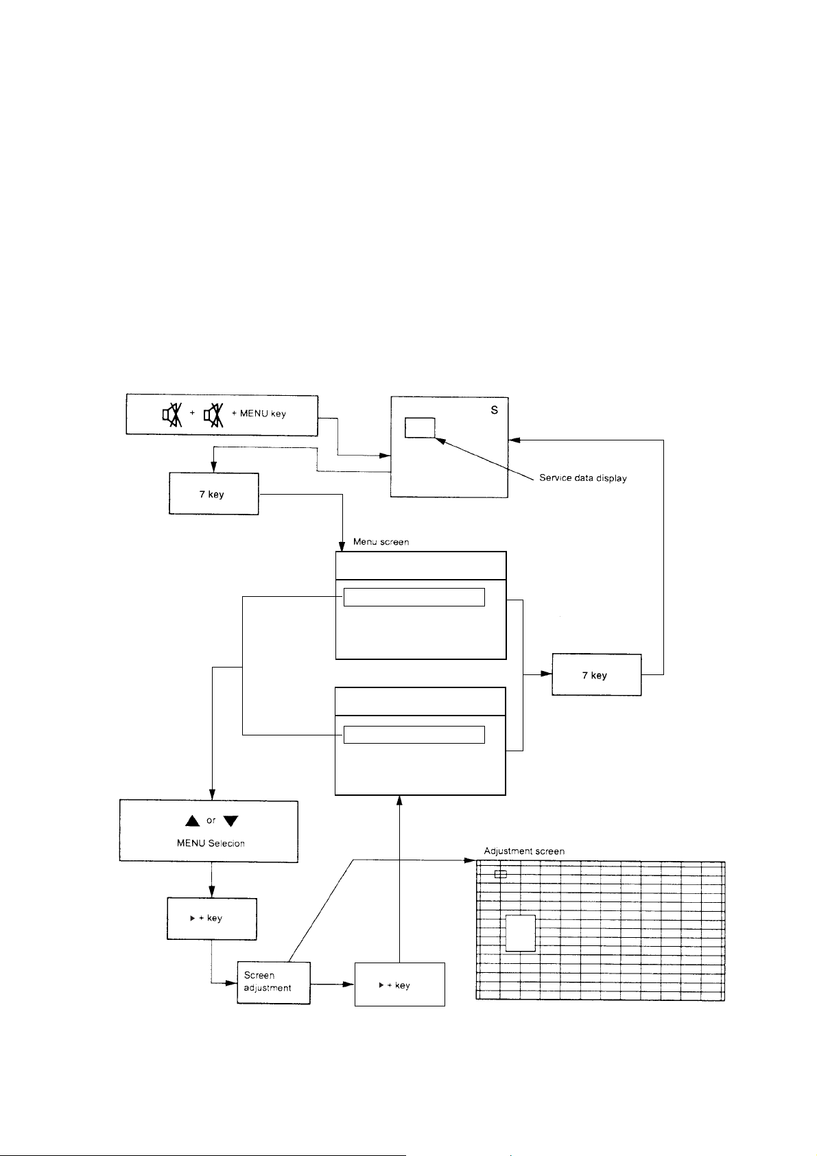
SERVICE MODE
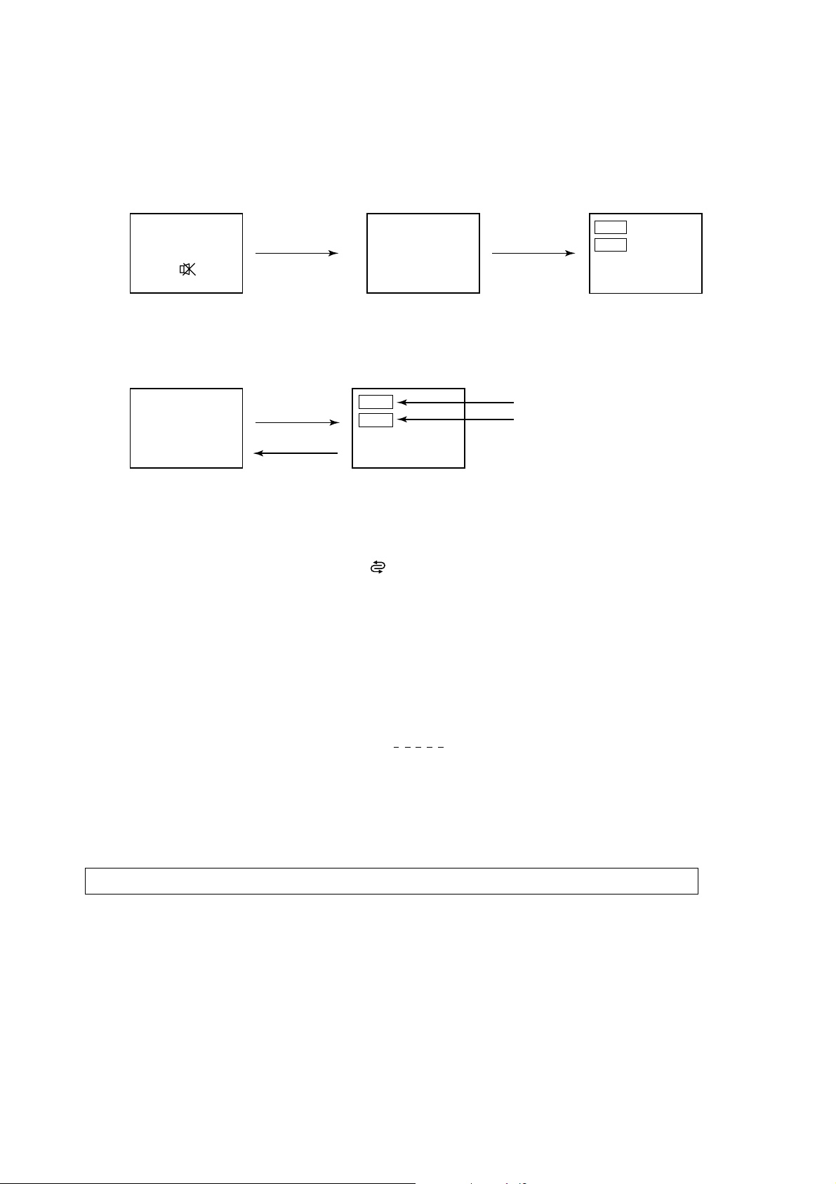
1. ENTERING TO SERVICE MODE
S
(Service mode display)
Item
Data
or Sound Mute
3) While pressing the o button,
press MENU button on TV set.
2) Press o button again to
keep pressing.
2. DISPLAYING THE ADJUSTMENT MENU
1) Press MENU button on TV.
3. KEY FUNCTION IN THE SERVICE MODE
The following key entry during display of adjustment menu provides special functions.
Screen adjustment mode ON/OFF: -/-- (
) button (on Remote)
Test signal selection : a button (on Remote)
Selection of the adjustment items : Channel s/t (on TV or Remote)
Change of the data value : Volume ; +/– (on TV or Remote)
Adjustment menu mode ON/OFF : MENU button (on TV)
Initialization of the memory (QA02) : CALL + Channel button on TV (s)
Reset the count of operating protect
circuit to “00”: CALL + Channel button on TV (t)
“RCUT” selection : 1 button
“GCUT” selection : 2 button
“BCUT” selection : 3 button
“SCNT” selection : 4 button
“COLP” selection : 5 button
“TNTC” selection : 6 button
Convergence adj : YELLOW button
Self diagnostic display ON/OFF : 9 button
1) Press o button once on
Remote Control.
Adjustment mode
Press
Press
Service mode
Item
Data
S
Color thickness correction
note: Displayed differently as shown below, de-
pending on the setting of the receiving color
system.
COLP (PAL)
COLC (NTSC)
COLS (SECAM)
CAUTION : Never try to perform initialization unless you have changed the memory IC.
-
10
-
Page 11

4. SELECTING THE ADJUSTING ITEMS
1) Every pressing of CHANNEL button in the service mode changes the adjustment items in the order of table-2.
( button for reverse order)
Refer to table-2 for preset data of adjustment mode.
(See SETTING & ADJUSTING DATA on page 26)
5. ADJUSTING THE DATA
1) Pressing of VOLUME +/– button will change the value of data in the range from 00H to FFH. The variable
range depends on the adjusting item.
6. EXIT FROM SERVICE MODE
1) Pressing POWER button to turn off the TV once.
INITIALIZATION OF MEMORY DATA OF QA02
After replacing QA02, the following initialization is required.
1. Enter the service mode, then select any register item.
2. Press and hold the CALL button on the Remote, then press the CHANNEL button on the TV. The initialization of QA02 has
been complated.
3. Check the picture carefully. If necessary, adjust any adjustment item above.
Perform “Auto search Memory” on the owner’s manual.
CAUTION: Never attempt to initialize the data unless QA02 has been replaced.
-
11
-
Page 12

8. SELF DIAGNOSTIC FUNCTION
1) Press “9” button on Remote Control during display of adjustment menu in the service mode.
The diagnosis will begin to check if interface among IC’s are executed properly.
2) During diagnosis, the following displays are shown.
Indicated color of mode now selected : Green and Red
<SELF CHECK>
2300* * * *(SAA556*PS/M3/* * * *)
TIME : 000000
POWER : 0
BUS LINE : OK
BUS CONT : OK
BLOCK : UV V1 V2 V3
Indicated color of other modes : Black
Green : Normal
Red : The microcomputer operates to provide judgement
of no video signal. The red color is still indicated
though the signal is input, failure may exist in input
signal line including QV01.
NOTE: (1) In case that "on timer" indicator is blinking with
interval of 0.5 seconds; it means protecting
circuit (Current limiter) is operating, and circuit components may possibly be damaged.
Check related components.
(2) In case that "on timer" indicator is blinking with
interval of 1 second; Protecting circuit does
Part number of microcomputer (QA01)
Total hour of turn the TV on. (Unit: H)
not operate, but a part of Bus line does not
operate normally. Check Bus line.
Operation number of protecting circuit ----“00” is nor-
mal.
When indication is other than “00”, overcurrent apts to
flow, and circuit parts may possibly be damaged.
BUS LINE ----“OK” is normal.
When indication shows “SDA-GND”, the SDA line may
possibly be shorted to GND..
BUS CONT ----“OK” is normal.
When indication shows “Q uuu NG”, the device with
the number may possibly be damaged.
BLOCK
UV : TV reception mode
V1 : VIDEO 1 input mode (a1)
V2 : VIDEO 2 input mode (a2)
V3 : VIDEO 3 input mode
( 3)
The items marked with are not usable to display in the SELF DIAGNOSTIC FUCTION for some model.
*
-
12
-
Page 13

1. ENTERING TO DESIGN MODE
1) Select the Service mode.
DESIGN MODE
2) While pressing CALL button on Remote
and press MENU button on TV.
3) Press MENU button on TV.
S D
(Design mode) (Adjustment mode)
Press
Press
ITEM
DATA
2. SELECTING THE ADJUSTING ITEMS
Every pressing of CHANNEL button in the design mode changes the adjustment items in the order of table-3.
( button for reverse order)
Refer to table-3 for data of design mode.
(See SETTING & ADJUSTING DATA on page 26)
3. ADJUSTING THE DATA
Pressing of VOLUME or button will change the value of data.
-
13
-
Page 14
ELECTRICAL ADJUSTMENT
ITEM ADJUSTMENT PROCEDURE
WIDTH
(WID)
VERTICAL LINEARITY
(VLIN)
HEIGHT
(HIT)
1. Call up the adjustment mode display, then select the item WID.
2. Press the VOLUME t button to get the picture so the left
or right edges of raster begins to lack.
3. Press the VOLUME s button to advance the data by 12
steps.
Note : Check the horizontal picture position is correct.
1. Call up the adjustment mode display, then select the item VLIN.
2. Receive the cross-hatch pattern which appears on the screen by the signal
generator.
3. Press the VOLUME s or t button to
obtain the picture of the best linearity
Center
1. Call up the adjustment mode display, then select the item HIT.
2. Press the VOLUME t button to get the picture so the top or bottom of
raster begins to lack.
3. Press the VOLUME s button to advance the data by 11 steps.
Note : Check the vertical picture position is correct.
WHITE BALANCE
(RCUT)
(GCUT)
(BCUT)
(RDRV)
(BDRV)
Black and White pattern
High light area
Adjust "RDRV" or "BDRV" to be white.
Low light area
Fine adjust "RCUT", "GCUT" or "BCUT" to be black.
1. Set user control to reset position.
CONTRAST → Max
(
BRIGHTNESS, COLOR, TINT → Center.
2. Call up the adjustment mode display, then select the item RCUT.
3. Adjust the data of items RCUT, GCUT, and BCUT to "40H".
4. Press the -/-- button on Remote. (Y-MUTE : ON)
5. Gradually rotate R, G and B screen volume of FOCUS PAC clockwise or counterclockwise until the raster appears slightly on the CRT through the each lens,
and leave them.
(Lookin to the lens in order to check the raster.)
6. Press the -/-- button on Remote. (Return to Normal Picture)
7. Press the a button on Remote, and select the Black and White pattern.
8. Adjust the data of items RCUT, GCUT and BCUT for proper white-balanced
picture in low light area.
9. Adjust the data of items RDRV and BDRV for proper white-balanced picture in
high light area.
10. Check the white balance in both low and high light areas.
If necessary, perform again steps from 8 to 9.
)
-
14
-
Page 15
Reference factory adjustment
TP-V
TP-G
Adjusting
standards
ight 4±1.5 lines
vel up to the 3.25±0.1V(p-p)
Adjusting methods
0.05V(p-p)
±
1.6±0.05V(p-p)
2.10
ainbow color bar.
W/B, SCNT.
Applied the Image MUTE.
signals.
1) Adjust the amplitude of the r
2) Adjust after adjusting
Adjust the amplitude of the color bar.
1)2)3)
mV
mV
10
10
±
0
t can
±
0
t can
Point that
starts lighting
y Tube and
ts lighting.
For details,
or each tube of G, R,
y repeating electrical focus and
vel of H.BLK.
vel of H.BLK.
vel of black and white signal par
vel of black and white signal par
VR to the point that star
Adjust the P-P value of the upper half.
(Y mute, DRV.CUT=40H)
adjust the screen
and B.
3) Directly observe the surface of Cathode Ra
4) Make above-mentioned adjustments f
1) Adjust to the best position b
refer to [focus
adjusting
method]
introduced in
the next page.
8750k-0.002uv
8750k-0.002uv
).
2
).
2
or each tube of G, R,
T except the axes under
.
ature of the bright part (103cd/m
ature of the dark part (17cd/m
adjustment.
and B.
2) Use the jig and shade the CR
3) Make above-mentioned adjustments f
± 25mV
0
Digital
voltmeter
y VCEN data.
oltmeter between TP-V
and TP-G and adjust it to 0 mV b
(No designation on polarity of degital voltmeter)
SIGNAL unit 2) Adjust the P-P value of the upper half.
(PAL)
(PAL-I signal) SIGNAL unit white peak.
WIDE mode signal adjustment
Audio system: I
center
signal
PA L
center
Items Names Settings Input signals Measuring points
BRTC Sub-bright Picture mode 1 Sub-bright Screen 1) Adjust the number of black collapsed lines of sub-br
SCNT Sub-contrast Picture mode 1 Sub-bright signal TP46B 1) Adjust amplitude from the pedestal le
COLP Sub-color Picture mode 1 Sub-bright TP46B
COLS Sub-color Picture mode 1 SECAM TP46B
color bar SIGNAL unit
SECAM TP02 1) Adjust so that the le
SECAM
center
R-Y Black level color bar SIGNAL unit be aligned with the le
SRY SECAM
CRT tubular 1) Darken the environment as much as possible.
screen 2) Set to factory-set screen adjusting MODE.
SECAM TP01 1) Adjust so that the le
color bar SIGNAL unit be aligned with the le
adjusting mode
R-Y Black level
SBY SECAM
Screen Screen Factory screen
adjustment
(PAL-I) adjustment optical focus adjustments
Crosshatch
signal
Picture mode 1 Retma signal Screen
Focus Focus
adjustment
Screen 1) Adjust the color temper
adjustment
adjustment
icture mode 1
icture mode 1 Screen 1) Adjust the color temper
WIDE mode
Picture mode 1 Phillips Pattern Between TP-V 1) Connect a digital v
WIDE mode
DFS-100 Hz and TP-G
Dark part W/B P
voltage
voltage
VW/B
BDR
RCUT
BCUT
RDRV Bright part P
VCEN Midpoint
adjustment
-
15
-
Page 16

Adjustment items Adjusting methods
Focus adjustment (Conditions)
- User adjustment: Dynamic mode, Cinema mode
- To be performed after centering magnet adjustment.
- Signal : Lens: R .... Crosshatch (PAL)
Electrical focus :
(Adjustment)
1. Common item
1) Make coarse adjustments in advance on the lens focus and electrical
focus of each R, G, and B tube.
2. G adjustment
1) Set to the G monochrome by lens cap.
2) Receive the image of crosshatch.
G.... Crosshatch (PAL)
B .... Crosshatch (PAL)
R .... Crosshatch (PAL)
G.... Crosshatch (PAL)
B .... Crosshatch (PAL)
3) Adjust the G electric focus.
Adjust the G electrical focus by the focus volume of focus block (Z410)
so that the screen center will come to optimum focus. (Although the G
electrical focus is to be adjusted to allow the scanning lines in the center
of the screen to be seen most clealy, if G alignment and astigmatism are
inferior with the appearance of vertical and horizontal flares in the center
of and around the screen and if the lines become thicker, adjust to the
best point observing the entire screen.)
4) Adjust the G lens focus.
Keep an eye on the center of the crosshatch pattern and adjust so that
the screen center will become clear.
As a rough guide to decrease unevenness, adjust so that red flares on
both sides of the crosshatch line will come to 1mm in thickness.
5) Repeat 3, 4, and attempt to further improve the focus quality.
-
16
-
Page 17
Adjustment items Adjusting methods
Focus adjustment
Concerning items 1), 2), 3), and 5) of G adjustment, these are common to the ones
on the previous page.
3. R adjustment
1) Set to the R monochrome by lens cap.
2) Receive the image of the internal crosshatched pattern.
3) Adjust the R electrical focus.
Adjust by focus volume of the focus block (Z410) so that the screen center will
come to optimum focus.
4) Adjust the R lens focus.
Adjust so that the screen center will become the best.
5) Repeat 3, 4, and attempt to further improve the focus quality.
4. B adjustment
2/3L
1) Set to the B monochrome by lens cap.
2) Receive the image of internal crosshatch
pattern.
L
3) Adjust the B electrical focus.
Adjust the B electrical focus by using the focus VR on the focus block (Z410)
so that the scanning line is the most distinct at the point of 2/3L left side from
the screen center.
4) Adjust the B lens focus.
Pay attention to the border of the blue line and the black (background) in the vicinity of the screen center.
First of all, make coarse adjustments of the lens, and move the lens adjusting
screw to the right at the point being considered as the best focus. Then, the lines
of the border become clear. Check and confirm under the circumstance that a
flare appears. On the contrary, if the lens adjusting screw is moved to the left from
the situation, the flare will disappear, and at this point you will find a point from
which the borderline itself begins to go out of focus. Adjust to the very point where
the focus begins to go out.
-
17
-
Page 18

Adjusting
standards
8 ± 1 flags
e
n
r
k of th
k of the Phillips patte
Adjusting methods
dummy screen and the cross mar
can overlap precisely.
This will be carried out individually for the tubes of R, G, and B.
1) Adjust the vertical and horizontal screen positions using
(Caution) Do not move HPOS and VPOS data.
VLIN.
e
y th
ertically. If not, adjust
hen VLIN is adjustd, adjust the screen position b
lower flags appear on the screen.
1) Shorten the vertical amplitude by HIT data until the upper and
centering magnet.
2) The amplitude should be balanced v
3) Subsequently, lengthen the vertical amplitude by HIT data until
.
e
y
ten the amplitude
y WID data so that th
ight flags appear completel
izontal amplitude b
either upper or lower flag end is aligned with the screen end.
2) Lengthen the hor
.
y the mask.
ertically.
k to the left screen edge
ks will come to 8 in total (each 4 flags
number of register mar
at the left and right sides).
Settings Input signals Measuring points
Picture model Philips Pattern Screen
Items Names
Adjustment
adjustment the centering magnet so that the center cross mar
)
AL-I
(P
DFS-100Hz (PAL-I)
of screen
position
CMUT-ON
ertical Picture model Philips Pattern
amplitude DFS-100Hz
adjustment
HITV
VLIN
PALW
WIDE
Screen 1) Lower the WID data in the beginning, and shor
Horizontal Picture mode 1 Philips Pattern
WID
adjustment horizontally until the left and r
CMUT-ON
DFS-100Hz (PAL-I)
adjustment
amplitude
Screen 1) Adjust to touch 16:9 frames of the The upper part of a screen.
adjustment
(PAL-I)
16:9 mode
CMUT-ON
Picture mode 1 Philips Pattern
amplitude
Vertical
adjustment
NTSC
HIT
adjustment 2) The amplitude should be balanced v
signal adjustment
DFS-120Hz signal
Picture mode 1 Monoscope Screen 1) The upper first one on the screen is to be hidden b
Vertical
adjustment
NHIT
NLIN amplitude
DFS-120Hz
Picture mode 1 Monoscope Screen 1) Adjust the 2.5th left register mar
amplitude
NTSC
NWID Vertical
Screen 1) Adjust to touch 16:9 frames of the The upper part of a screen.
adjustment
(PAL-I)
mode
adjustment
16:9 mode
Picture mode 1 Philips Pattern
amplitude
Vertical
NTSC
NHIT
adjustment
NTSC
-
18
-
Page 19
1. SCREEN ADJUSTMENT
CONVERGENCE ADJUSTMENT
The adjustment is carried out on four screens; 4 : 3 and 16 : 9
screens in both PAL and NTSC modes. When making the adjustments, feed an external signal to make an synchronization.
Note:
The convergence circuit is a circuit to eliminate screen distortion and can not make a drastic correction such as to correct
entire screen size. An excessive correction may actuate the
protection circuit. So a care will be necessary.
1-1. Entering the Adjustment Menu
When receiving
PAL (50Hz)
Conver Adjust MENU
Before proceeding to the adjustment for each screen, always
perform the adjustments for vertical size (HIT) and horizontal
size (WID) with the main deflection data changed.
Order of the adjusting screens is PAL 4 : 3 → PAL 16 : 9 →
NTSC 4 : 3 → NTSC 16 : 9.
The menu order is 1 → 2 → 3 .... when the vertical sync is 50
Hz. (In this case, item 4~6 are not displayed)
The menu order is 4 → 5 → 6 .... when the vertical sync is 60
Hz. (In this case, item 1~3 are not displayed)
When receiving
NTSC (60Hz)
1. Adjust PAL (50 Hz) 4:3
2. PALL 4:3 to Others
3. Adjust PAL 16:9
or
Conver Adjust MENU
4. Adjust NTSC (60 Hz) 4:3
5. NTSC 4:3 to NTSC 16:9
6 Adjust NTSC 16:9
-
Fig. 1
19
-
Page 20
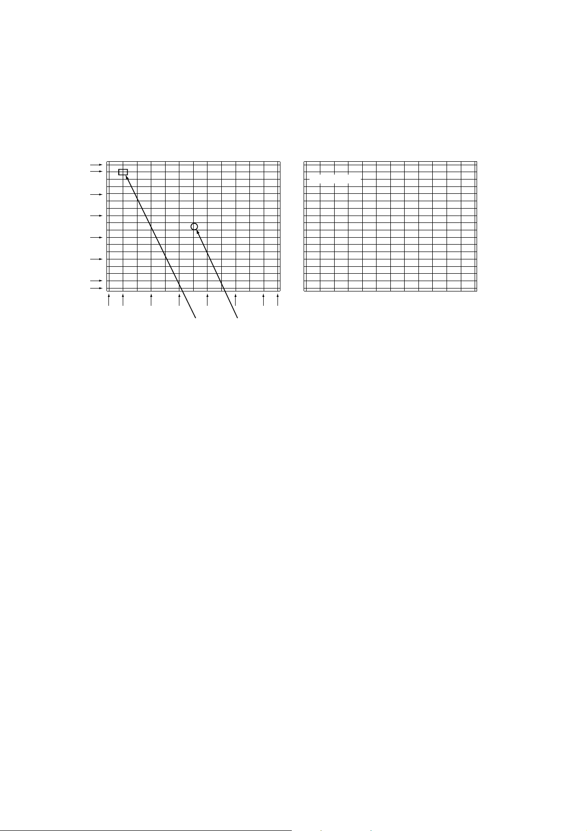
2. Picture
a) 50 Hz mode (PAL) . . . . Correcting point: Horizontal 8 x Vertical 8 (Arrow marks denote correcting point)
The first picture
Screen centerCursor (red)
(Blinking)
The first picture
Crosshatch pattern. Pattern colors are three color display. Cursor is blinking in red. When changed, condition is last memory
state.
Cursor is .......... Data change mode in lighting,
Cursor shifting mode in blinking.
Display color shows the color that data change is possible.
(Note: Red is displayed in yellow.)
The second picture
When entering from the first picture to the second picture, correcting wave of convergence is muted for one second.
During this period, the changed data is transferred from RAM
Q701 to E2PROM Q711, and saved.
The second picture
Data display
The second picture is indicated with data on top left of the first
picture, therefore, convergence cannot be adjusted by this picture.
Caution:
, Receive suitable signal for adjustment. Centering of
green picture can be done in 50 Hz mode (PAL).
, Centering of 60 Hz mode (NTSC) can be adjusted by
convergence adjustment. Besides, decide the center
by cross pattern of static convergence in menu, and
adjust convergence from center to circumference.
-
20
-
Page 21

b) 60 Hz mode (NTSC) . . . . Correcting point: Horizontal 8 x Vertical 7 (Arrow marks denote correcting point)
The first picture
Cursor (red)
(Blinking)
Screen center
The first picture
Crosshatch pattern. Pattern colors are three color display. Cursor is blinking in red. When changed, condition is last memory
state.
Cursor is .......... Data change mode in lighting,
Cursor shifting mode in blinking.
Display color shows the color that data change is possible.
The second picture
When entering from the first picture to the second picture, correcting wave of convergence is muted for one second.
The second picture
Data display
During this period, the changed data is transferred from RAM
Q701 to E
2
PROM Q711, and saved.
The second picture is indicated with data on top left of the first
picture, therefore, convergence cannot be adjusted by this picture.
Caution:
, Receive suitable signal for adjustment. Decide the center
by cross pattern of static convergence in menu, and adjust
convergence from center to circumference.
-
21
-
Page 22

3. ADJUSTING PICTURE DIMENSION (GREEN PICTURE)
[4:3]
1. 50 Hz mode (PAL)
Screen center
310.
(318.0)
(63.5)
(63.5)
(318.0)
310.5
5
17mm
274
164.5
55
0
55
164.5
274
17mm
(360.0)
(191.0)
(191.0)
(360.0)
2. 60Hz mode (NTSC)
B
A
8.5mm 8.5mm
(496.0) (496.0)
372.5
(431.5) (431.5)(259.0) (259.0)(86.3) (86.3)
428.
5 428.5
74.5223.5
43 inches 4:3 Screen size: Horizontal 874mm, Vertical 655mm
Dimension A: 74.5mm, Dimension B: 36.5mm
372.5223.574.50
mark:
(H span) (V span)
center
( ): 50VJ33Q
Screen
center
(353.5)
306(353.5)
(151.5)
(303.0)
306
262(303.0)
131(151.5)
0
131
262
8.5mm 8.5mm
21.6mm
(496.0) (496.0)
327.5
(431.5) (431.5)(259.0) (259.0)(86.3) (86.3)
428.5
43 inches 4:3 Screen size: Horizontal 874mm, Vertical 655mm
Dimension A: 74.5mm, Dimension B: 43.7mm
Screen
center
327.5223.574.5074.5223.5
428.5
-
22
-
Page 23

4. ADJUSTING PICTURE DIMENSION (GREEN PICTURE)
[16:9]
1. 50 Hz mode (PAL)
Screen center
17mm
232.(270.2)
9
205.(238.4)
5
(143.2)
123.4
(47.9)
41.3
0
(47.9)
41.3
(143.2)
123.4
(238.4)
205.5
(270.2)
232.9
Screen
center
B
A
17mm
2. 60Hz mode (NTSC)
229.5
(265.2)
196.5
(227.3)
(113.6)
98.3
0
(113.6)
98.3
8.5mm 8.5mm
372.
5
(431.5) (431.5)(259.0) (259.0)(86.3) (86.3)
428.
5 428.5
(496.0) (496.0)
43 inches 4:3 Screen size: Horizontal 874mm, Vertical 655mm
Dimension A: 74.5mm, Dimension B: 27.4mm
(H span) (V span)
372.5223.574.5074.5223.5
mark:
( ): 50VJ33Q
center
Screen
center
(265.2)
(227.3)
229.5
196.5
8.5mm 8.5mm
21.6mm
(496.0) (496.0)
327.5
(431.5) (431.5)(259.0) (259.0)(86.3) (86.3)
428.5
327.5223.574.5074.5223.5
43 inches 4:3 Screen size: Horizontal 874mm, Vertical 655mm
Dimension A: 74.5mm, Dimension B: 32.7mm
-
23
-
428.5
Page 24

5. Deflection amplitude setting (HIT/WID adjusting method under muted convergence)
* Green pattern under the muted convergence
B
A
0 point
1st flag
2nd flag
Castration border line
C
Screen edge
A
Horizontal amplitude: Left and right register marks of Philips pattern C + D = 8 (See A of the upper figure.)
Vertical amplitude: The point where the 3rd vertical line outer from the upper and lower register marks of Philips
pattern is overlapped with flags contacts the screen edge. If the amplitude is uneven horizontally
and vertically, make HIT adjustment so that B shown in the upper left of the upper figure comes to
contact the screen edge.
Next, pay attention to the C point. Check and confirm that the castration border line contacts
through 2nd line to 4th line outer from the lower register mark.
-
24
-
Page 25

SCREEN AND MIRROR ALIGNMENTS
ASSEMBLING AND MOUNTING OF
FRONT SCREEN
* Please refer to MECHANICAL DISASSEMBLY page 32.
CLEANING OF LENS AND MIRROR
CAUTION : Do not hold the optical system parts (lens and
mirror) with bare hand to avoid finger-prints on
the surface of those parts.
HOW TO CLEAN LENS AND MIRROR
1. Be sure to remove sand dust with an air brush, etc.
2. When it is stained slightly, breathe upon it and wipe away
with the specified cleaning cloth.
For other stains than the above, wipe the stains away with
the specified cloth into which a cleaning liquid has been
soaked.
Cleaning liquid ................... LENS LUSTER (Manufactured
by Edmund Scientific Co.), etc.
HOW TO CLEAN SCREEN
When cleaning the screen, use a soft cloth so as not to damage the screen.
1. Wipe the stain away with a diluted neutral detergent soaked
cloth.
2. Wipe the detergent away with a water soaked cloth.
3. Wipe the screen with a dry cloth to remove moisture on the
screen.
Note : Absolutely do not use alcohol, benzine, thinner, etc.
for cleaning in order not to wipe away the black print
on the surface.
-
25
-
Page 26

CIRCUIT CHECKS
HIGH VOLTAGE CHECK
CAUTION: There is no HIGH VOLTAGE ADJUSTMENT on this chassis. Checking should be done following the steps below.
1. Connect an accurate high voltage meter to the anode of the picture tube.
2. Turn on the receiver. Set the BRIGHTNESS and CONTRAST to minimum (zero beam current).
3. High voltage must be measured below (B) kV.
Refer to table-1 for high voltage (B).
(See SETTING & ADJUSTING DATA on page 27)
4. Vary the BRIGHTNESS to both extremes to be sure the high voltage does not exceed the limit under any conditions.
CAUTION:
When the following parts fail, check the High Voltage after replacing.
Location
No.
T461
C440
C443
C444
C467
C468
ANODE VOLTAGE MEASURING METHOD
CAUTION: Take extra precaution when measuring this high voltage. High voltages are also present in surrounding circuit
boards (CRT DRIVE assembly, DEFLECTION assembly, and POWER SUPPLY assembly).
1. Disconnect the FBT anode cable as outlined below. Measure high voltage at the point where the cable enters the FBT.
2. Holding the rubber cover firmly, turn it counterclockwise and check that the lock has been disengaged. (See Fig. b on page
8.)
3. Determine the extent of the rubber cover before disconnecting the cable.
4. Pull straight up the anode cable to disconnect.
5. When reconnecting the cable, proceed in the reverse order.
After reconnecting, tug on the cable to check that it is secure.
Name
Flyback Trans.
Capacitor
Capacitor
Capacitor
Capacitor
Capacitor
Name
TFB3091AD
1500pF, ±3%
4700pF, ±3%
3600pF, ±3%
12000pF, ±5%
12000pF, ±5%
-
26
-
Page 27

CHAPTER 2 SPECIFIC INFORMATIONS
SETTING & ADJUSTING DATA
SAFETY INSTRUCTIONS
HIGH VOLTAGE AT ZERO BEAM:
MAX HIGH VOLTAGE:
AC VOLTAGE
Table-1
SERVICE MODE
ADJUSTING ITEMS AND DATAS IN THE SERVICE MODE:
(A)
(B)
(C)
43"/50"
31.3 kV
33.3 kV
220~240 V
Item
RCUT
GCUT
BCUT
RDRV
BDRV
BRTC
COLP
COLS
SCNT
SRY
SBY
HIT
VLIN
WID
VCEN
DESIGN MODE
ADJUSTING ITEMS AND DATAS IN THE DESIGN MODE:
Item Name of adjustment Preset Data (43"/50") Remarks
R CUTOFF (B/W)
G CUTOFF (B/W)
B CUTOFF (B/W)
R DRIVE
B DRIVE
BRIGHT CEN
COLOR CEN PAL
COLOR CEN SECAM
SUB CONTRAST FOR RF
SECAM R-Y BLACK LEVEL
SECAM B-Y BLACK LEVEL
PICTUR HEIGHT (Full)
V-LINEARITY (Full)
PICTURE WIDTH
V-CENTERING (Full)
Adjustment
Reference data
40H
40H
40H
40H
40H
40H
3CH
3CH
F0H
08H
08H
5CH
07H
22H
2AH
Table-2
OPT0 OPTION 0 80H
OPT1 OPTION 1 4AH
OPT2 OPTION 2 20H
OPT4 OPTION 4 01H
Table-3
-
27
-
Page 28

LOCATION OF CONTROLS
43VJ33Q 50VJ33Q
Power Button
RED-Power On
RED-Power On
Power Button
-
28
-
Page 29

To mute the sound
Teletext control buttons
To exit Menus
Bass Boost
No function on this model
To bring up on-screen information and
for the teletext initial/index function
To select input from external sources
To access sub-pages when in teletext
mode
To select mode
On-screen Menus
Selectable picture preferences
Aspect ratio (16:9 or 4:3)
Number buttons
To return to the previous programme
For On/Standby mode
To display teletext
When in VCR or DVD mode:
press
m
to PAUSE
press
w
to EJECT
press
l
q
to SKIP-REWIND
press
s
l
to SKIP-FORWARD
press
r
to PLAY
press
p
to STOP
press
q
to REWIND
press
s
to FAST FORWARD
To change programme positions and
teletext pages
To alter the volume
When using menus the arrows move the
cursor on the screen up, down, left or
right. OK to confirm your selection
When in TV mode:
u
No function on this model
O
I/II
Stereo/bilingual reception
8/9
Time display
When in Teletext mode:
r
To reveal concealed text
q
To hold a wanted page
s
To enlarge teletext display size
8/9
To select a page whilst viewing a
normal picture
Remote Control Key
-
29
-
Page 30

PROGRAMMING CHANNEL MEMORY
Auto tune
Before running Auto tune put your decoder and video
recorder to Standby. To set up the TV use the buttons
on the remote control.
To choose the required language, press MENU and
1
use
to select Set up from the top bar.
Press
2
Press or to select.
3
Choose your country from the options available.
4
Press
The TV will now tune the stations for your country.
Now press
5
select.
Your System will have been selected, if there is a
6
choice, please select from the systems displayed.
For UK only: Press OK to start and go to step 8.
B/G
D/K
Press to select your System. Press to highlight
7
START and then
to highlight Language.
to highlight Country. Then or to select.
to highlight Auto tuning, then to
-
Continental Europe, I - UK
-
Eastern Europe, L1, L2 - France
.
Programm skip
To prevent certain programmes from being viewed, the
programme position can be skipped and the remote
control removed. The television can then be watched as
normal using the controls on the side/front, but the set will
not show the skipped programme position.
Select Manual tuning from the Set up menu.
1
Use
2
3
4
5
or to highlight the programme position to
be skipped and press OK to select.
to select Programme skip.
Press
Use or to turn Programme skip on. Press OK.
*on the screen indicates a skipped programme
position.
Press MENU and repeat from Step 2 or press EXIT.
Each programme position has to be individually
selected. To turn Programme skip off, repeat the
procedure for each position.
Skipped programme positions cannot be selected
by P
( ) and P ( ) or by the controls on the side/
front of the TV, but can still be accessed by the
number buttons on the remote control.
The search will begin for all available stations.
8
will flash and the bullet will move along the line
as the search progresses.
You must allow the television to complete the search.
When the search is complete the TV will automati-
9
cally return to programme position 1.
This may not be a clear picture or the signal may be
weak, so the station order may be changed by using Programme sorting.
If the television cannot be connected to a video/decoder with a Scart lead or if a station on another
system is required, use Manual tuning to allocate a
programme position.
-
30
-
Page 31

K501
MECHANICAL DISASSEMBLY
K502
K601
Labels
A004
(A420)
A424
A225
A258
A201
K101
K102
K103
-
31
-
Page 32

CHASSIS AND CABINET REPLACEMENT PARTS LIST
WARNING: BEFORE SERVICING THIS CHASSIS, READ THE “X-RAY RADIATION PRECAUTION”, “SAFETY
PRECAUTION” AND “PRODUCT SAFETY NOTICE” ON PAGE 3 OF THIS MANUAL.
CAUTION: The international hazard symbols " " in the schematic diagram and the parts list designate com-ponents
which have special characteristics important for safety and should be replaced only with types identical to those in
the original circuit or specified in the parts list. The mounting position of replacements is to be identical with originals.
Before replacing any of these components, read carefully the PRODUCT SAFETY NOTICE. Do not degrade the
safety of the receiver through improper servicing.
NOTICE:
•
The part number must be used when ordering parts, in order to assist in processing, be sure to include the
Model number and Description.
•
The PC board assembly with ∗ mark is no longer available after the end of the production.
Model : 43VJ33Q / 50VJ33Q
Capacitors ............. CD : Ceramic Disk PF : Plastic Film EL : Electrolytic
Resistors ............... CF : Carbon Film CC : Carbon Composition MF : Metal Film
OMF : Oxide Metal Film VR : Variable Resistor FR : Fusible Resistor
(All CD and PF capacitors are ±5%, 50V and all resistors, ±5%, 1/6W unless otherwise noted.)
–
Location
Parts No. Description
No.
#1:[43VJ]
#2:[50VJ]
CAPACITORS
C101 24794470 ELECTROLYTIC, 16V 47UF M
C102 24109103 CERAMIC CHIP, 50V B 0.01UF K
C103 24762221 ELECTROLYTIC, 10V 220UF M
C104 24109103 CERAMIC CHIP, 50V B 0.01UF K
C105 24797100 ELECTROLYTIC, 50V 10UF M
C106 24109102 CERAMIC CHIP, 50V B 1000PF K
C107 24109103 CERAMIC CHIP, 50V B 0.01UF K
C108 24794101 ELECTROLYTIC, 16V 100UF M
C109 24109103 CERAMIC CHIP, 50V B 0.01UF K
C110 24109103 CERAMIC CHIP, 50V B 0.01UF K
C111 24109103 CERAMIC CHIP, 50V B 0.01UF K
C112 24503049 PLASTIC FILM, 63V 0.47UF J
C113 24109103 CERAMIC CHIP, 50V B 0.01UF K
C114 24109103 CERAMIC CHIP, 50V B 0.01UF K
C115 24109103 CERAMIC CHIP, 50V B 0.01UF K
C116 24109103 CERAMIC CHIP, 50V B 0.01UF K
C117 24105470 CERAMIC CHIP, 50V CH 47PF J
C118 24794101 ELECTROLYTIC, 16V 100UF M
C119 24793101 ELECTROLYTIC, 10V 100UF M
C120 24109103 CERAMIC CHIP, 50V B 0.01UF K
C122 24109103 CERAMIC CHIP, 50V B 0.01UF K
C123 24100102 CERAMIC CHIP, 50V F 1000PF Z
C124 24797478 ELECTROLYTIC, 50V 0.47UF M
C125 24669479 ELECTROLYTIC, 50V 4.7UF M 3A
C126 24590472 PLASTIC FILM, 50V 4700PF J
C127 24797478 ELECTROLYTIC, 50V 0.47UF M
C128 24794100 ELECTROLYTIC, 16V 10UF M
C129 24794100 ELECTROLYTIC, 16V 10UF M
C130 24109103 CERAMIC CHIP, 50V B 0.01UF K
C140 24109103 CERAMIC CHIP, 50V B 0.01UF K
C160 24567224 PLASTIC FILM, 50V 0.22UF J
C170 24567104 PLASTIC FILM, 50V 0.1UF J
C202 24109103 CERAMIC CHIP, 50V B 0.01UF K
C204 24797010 ELECTROLYTIC, 50V 1UF M
C205 24092538 CERAMIC CHIP, 10V F 1UF Z
C206 24794470 ELECTROLYTIC, 16V 47UF M
C214 24503047 PLASTIC FILM, 63V 0.33UF J
C307 24503049 PLASTIC FILM, 63V 0.47UF J
C309 24591102 PLASTIC FILM, 50V 1000PF J
C310 24667101 ELECTROLYTIC CE04Q, 25V 100UF M 3A
Location
Parts No. Description
No.
C311 24567103 PLASTIC FILM, 50V 0.01UF J
C314 24092730 CERAMIC CHIP, 16V B 0.1UF K
C320 24669101 ELECTROLYTIC, 50V 100UF M 3A
C321 24669101 ELECTROLYTIC, 50V 100UF M 3A
C324 24669101 ELECTROLYTIC, 50V 100UF M 3A
C325 24503045 PLASTIC FILM, 63V 0.22UF J
C327 24503045 PLASTIC FILM, 63V 0.22UF J
C329 24669100 ELECTROLYTIC, 50V 10UF M 3A
C330 24085946 ELECTROLYTIC, NONPOLAR, 16V 10UF M 3A
C332 24669221 ELECTROLYTIC, 50V 220UF M 3A
C333 24693473 PLASTIC FILM, 100V 0.047UF J
C335 24503041 PLASTIC FILM , 63V 0.1UF J
C338 24666330 ELECTROLYTIC, 16V 33UF M 3A
C340 24666330 ELECTROLYTIC, 16V 33UF M 3A
C370 24669229 ELECTROLYTIC, 50V 2.2UF M 3A
C371 24092730 CERAMIC CHIP, 16V B 0.1UF K
C401 24214821 CERAMIC DISC, 500V B 820PF K
C402 24214391 CERAMIC DISC, 500V B 390PF K
C404 24212152 CERAMIC DISC, 50V B 1500PF K
C405 24567124 PLASTIC FILM, 50V 0.12UF J
C406 24678100 ELECTROLYTIC, 200V 10UF M 3A
C410 24667102 ELECTROLYTIC, 25V 1000UF M 3A
C412 24828104 PLASTIC FILM, 200V 0.1UF J
C415 24092484 CERAMIC DISC, 2KV B 1500PF K
C416 24828333 PLASTIC FILM, 200V 33000PF J
C417 24679229 ELECTROLYTIC, 250V 2.2UF M 3A
C423 24503293 PLASTIC FILM CF92 T 400V R39UF J
C426 24211222 CERAMIC DISC, 2KV B 2200PFK
C432 24567223 PLASTIC FILM, 50V 0.022UF J
C433 24567473 PLASTIC FILM, 50V 47000PF J
C440 24503063 PLASTIC FILM, 1800VH 1500PF H
C443 24503146 PLASTIC FILM, 1500VH 4700PF H
C444 24082943 PLASTIC FILM, 1500VH 3600PF H
C445 24828473 PLASTIC FILM, 200V 0.047UF J
C446 24679330 ELECTROLYTIC, 250V 33UF M 3A
C448 24073118 ELECTROLYTIC, 160V 33UF M
C449 24214221 CERAMIC DISC, 500V B 220PF K
C460 24679479 ELECTROLYTIC, 250V 4.7UF M 3A
C463 24567333 PLASTIC FILM, 50V 33000PF J
C464 24503343 PLASTIC FILM, 100V 3.3UF K
C465 24567103 PLASTIC FILM, 50V 0.01UF J
C466 24591472 PLASTIC FILM, 50V 4700PF J
C467 24820123 PLASTIC FILM, 630V 0.012UF J
C468 24820123 PLASTIC FILM, 630V 0.012UF J
-
32
-
Page 33

Location
No.
Parts No. Description
Location
No.
Parts No. Description
C481 24666101 ELECTROLYTIC 04Q, 16V 100UF M 3A
C482 24591223 PLASTIC FILM, 50V 0.022UF J
C483 24591223 PLASTIC FILM, 50V 0.022UF J
C484 24591102 PLASTIC FILM, 50V 1000PF J
C491 24666100 ELECTROLYTIC, 10V 10UF M 3A
C497 24503049 PLASTIC FILM, 63V 0.47UF J
C498 24669479 ELECTROLYTIC, 50V 4.7UF M 3A
C501 24100104 CERAMIC CHIP, 25V F 0.1UF Z
C502 24092743 CERAMIC CHIP, 10V F 0.47UF Z
C503 24794470 ELECTROLYTIC, 16V 47UF M
C504 24109103 CERAMIC CHIP, 50V B 0.01UF K
C511 24100104 CERAMIC CHIP, 25V F 0.1UF Z
C512 24100104 CERAMIC CHIP, 25V F 0.1UF Z
C513 24100104 CERAMIC CHIP, 25V F 0.1UF Z
C514 24794470 ELECTROLYTIC, 16V 47UF M
C516 24105110 CERAMIC CHIP, 50V CH 11PF J
C517 24092734 CERAMIC CHIP, 16V F 0.22UF Z
C522 24109103 CERAMIC CHIP, 50V B 0.01UF K
C524 24109103 CERAMIC CHIP, 50V B 0.01UF K
C526 24109222 CERAMIC CHIP, 50V B 2200PF K
C540 24100104 CERAMIC CHIP, 25V F 0.1UF Z
C541 24100104 CERAMIC CHIP, 25V F 0.1UF Z
C542 24100104 CERAMIC CHIP, 25V F 0.1UF Z
C601 24669010 ELECTROLYTIC, 50V 1UF M 3A
C602 24669010 ELECTROLYTIC, 50V 1UF M 3A
C603 24591102 PLASTIC FILM, 50V 1000PF J
C604 24591102 PLASTIC FILM, 50V 1000PF J
C605 24669010 ELECTROLYTIC, 50V 1UF M 3A
C606 24669010 ELECTROLYTIC, 50V 1UF M 3A
C607 24667470 ELECTROLYTIC CE04Q, 25V 47UF M 3A
C608 24667470 ELECTROLYTIC CE04Q, 25V 47UF M 3A
C609 24667470 ELECTROLYTIC CE04Q, 25V 47UF M 3A
C610 24669479 ELECTROLYTIC, 50V 4.7UF M 3A
C612 24669102 ELECTROLYTIC, 50V 1000UF M 3A
C613 24503042 PLASTIC FILM, 63V 0.12UF J
C614 24503042 PLASTIC FILM, 63V 0.12UF J
C615 24669102 ELECTROLYTIC, 50V 1000UF M 3A
C616 24669102 ELECTROLYTIC, 50V 1000UF M 3A
C617 24669220 ELECTROLYTIC, 04Q 50V 22UF M 3A
C618 24669478 ELECTROLYTIC, 50V 0.47UF M 3A
C619 24794471 ELECTROLYTIC, 16V 470UF M
C621 24669229 ELECTROLYTIC, 50V 2.2UF M 3A
C622 24591223 PLASTIC FILM, 50V 0.022UF J
C623 24797479 ELECTROLYTIC, 50V 4.7UF M
C624 24795101 ELECTROLYTIC, 25V 100UF M
C625 24795221 ELECTROLYTIC CE04G, 25V 220UF M
C639 24793101 ELECTROLYTIC, 10V 100UF M
C701 24105330 CERAMIC CHIP, 50V CH 33PF J
C702 24105330 CERAMIC CHIP, 50V CH 33PF J
C703 24105330 CERAMIC CHIP, 50V CH 33PF J
C704 24105330 CERAMIC CHIP, 50V CH 33PF J
C706 24100104 CERAMIC CHIP, 25V F 0.1UF Z
C707 24100104 CERAMIC CHIP, 25V F 0.1UF Z
C708 24100104 CERAMIC CHIP, 25V F 0.1UF Z
C710 24100104 CERAMIC CHIP, 25V F 0.1UF Z
C712 24105330 CERAMIC CHIP, 50V CH 33PF J
C713 24105330 CERAMIC CHIP, 50V CH 33PF J
C714 24100104 CERAMIC CHIP, 25V F 0.1UF Z
C715 24092730 CERAMIC CHIP, 16V B 0.1UF K
C716 24092730 CERAMIC CHIP, 16V B 0.1UF K
C719 24794101 ELECTROLYTIC, 16V 100UF M
C721 24105070 CERAMIC CHIP, 50V CH 7PF D
C724 24100104 CERAMIC CHIP, 25V F 0.1UF Z
C725 24100104 CERAMIC CHIP, 25V F 0.1UF Z
C726 24100104 CERAMIC CHIP, 25V F 0.1UF Z
C727 24100104 CERAMIC CHIP, 25V F 0.1UF Z
C730 24100104 CERAMIC CHIP, 25V F 0.1UF Z
C731 24100104 CERAMIC CHIP, 25V F 0.1UF Z
C732 24109103 CERAMIC CHIP, 50V B 0.01UF K
C735 24092730 CERAMIC CHIP, 16V B 0.1UF K
C736 24100104 CERAMIC CHIP, 25V F 0.1UF Z
C739 24100104 CERAMIC CHIP, 25V F 0.1UF Z
C740 24100104 CERAMIC CHIP, 25V F 0.1UF Z
C741 24794470 ELECTROLYTIC, 16V 47UF M
C742 24794470 ELECTROLYTIC, 16V 47UF M
C743 24100104 CERAMIC CHIP, 25V F 0.1UF Z
C744 24100104 CERAMIC CHIP, 25V F 0.1UF Z
C745 24794470 ELECTROLYTIC, 16V 47UF M
C746 24794470 ELECTROLYTIC, 16V 47UF M
C747 24100104 CERAMIC CHIP, 25V F 0.1UF Z
C748 24100104 CERAMIC CHIP, 25V F 0.1UF Z
C749 24794470 ELECTROLYTIC, 16V 47UF M
C750 24794470 ELECTROLYTIC, 16V 47UF M
C761 24105102 CERAMIC CHIP, 25V CH 1000PF J
C762 24590562 PLASTIC FILM, 50V 5600PF J
C763 24105391 CERAMIC CHIP, 50V CH 390PF J
C765 24105102 CERAMIC CHIP, 25V CH 1000PF J
C766 24590562 PLASTIC FILM, 50V 5600PF J
C767 24105391 CERAMIC CHIP, 50V CH 390PF J
C769 24105102 CERAMIC CHIP, 25V CH 1000PF J
C770 24590562 PLASTIC FILM, 50V 5600PF J
C771 24105391 CERAMIC CHIP, 50V CH 390PF J
C772 24761221 ELECTROLYTIC, 6.3V 220UF M
C773 24105102 CERAMIC CHIP, 25V CH 1000PF J
C774 24590562 PLASTIC FILM, 50V 5600PF J
C775 24105391 CERAMIC CHIP, 50V CH 390PF J
C777 24105102 CERAMIC CHIP, 25V CH 1000PF J
C778 24590562 PLASTIC FILM, 50V 5600PF J
C779 24105391 CERAMIC CHIP, 50V CH 390PF J
C781 24105102 CERAMIC CHIP, 25V CH 1000PF J
C782 24590562 PLASTIC FILM, 50V 5600PF J
C783 24105391 CERAMIC CHIP, 50V CH 390PF J
C784 24105821 CERAMIC CHIP, 25V CH 820PF J
C785 24105821 CERAMIC CHIP, 25V CH 820PF J
C786 24105821 CERAMIC CHIP, 25V CH 820PF J
C787 24105821 CERAMIC CHIP, 25V CH 820PF J
C788 24105821 CERAMIC CHIP, 25V CH 820PF J
C789 24105821 CERAMIC CHIP, 25V CH 820PF J
C795 24761221 ELECTROLYTIC, 6.3V 220UF M
C798 24763101 ELECTROLYTIC, 16V 100UF M
C799 24763101 ELECTROLYTIC, 16V 100UF M
C801 24503055 PLASTIC FILM, AC275V 0.22UF M
C802 24092569 CERAMIC DISC, AC250V E 2200PF M
C803 24092569 CERAMIC DISC, AC250V E 2200PF M
C804 24092570 CERAMIC DISC, AC250V E 3300PF M
C805 24092569 CERAMIC DISC, AC250V E 2200PF M
C806 24092569 CERAMIC DISC, AC250V E 2200PF M
C808 24503506 PLASTIC FILM, AC275V 0.1UF K
C810 24073121 400V 560M 20KH LLQ2G561MHSGTL
C811 24092281 CERAMIC DISC, AC250V E 4700PF
C813 24092281 CERAMIC DISC, AC250V E 4700PF
C814 24503115 PLASTIC FILM, 800V 0.022UF J
C820 24503055 PLASTIC FILM, AC275V 0.22UF M
C821 24073098 ELECTROLYTIC, 450V 4.7UF M 3A
C823 24667221 ELECTROLYTIC CE04Q, 25V 220UF M 3A
C824 24667221 ELECTROLYTIC CE04Q, 25V 220UF M 3A
C829 24214103 CERAMIC DISC, 500V B 0.01UF K
C830 24669100 ELECTROLYTIC, 50V 10UF M 3A
C831 24073037 ELECTROLYTIC, 16V 47UF M 3A @U902
24503041 PLASTIC FILM , 63V 0.1UF J @U903
C834 24669100 ELECTROLYTIC, 50V 10UF M 3A
C835 24073015 ELECTROLYTIC, 10V 47UF M 3A
C840 24667101 ELECTROLYTIC CE04Q, 25V 100UF M 3A
C841 24617026 ELECTROLYTIC 04CP, 16V 820UF M
C842 24669220 ELECTROLYTIC, 04Q 50V 22UF M 3A
C857 24667332 ELECTROLYTIC, 25V 3300UF M 3A
C858 24667332 ELECTROLYTIC, 25V 3300UF M 3A
C863 24503045 PLASTIC FILM, 63V 0.22UF J
-
33
-
Page 34

Location
No.
Parts No. Description
Location
No.
Parts No. Description
C864 24092474 CERAMIC DISC, 2KV B 220PF K
C866 24503049 PLASTIC FILM, 63V 0.47UF J
C867 24591682 PLASTIC FILM, 50V 6800PF J
C868 24668470 ELECTROLYTIC, 35V 47UF M 3A
C869 24678229 ELECTROLYTIC, 200V 2.2UF M 3A
C870 24503122 PLASTIC FILM CQ92 T 800V 82000PF J
C871 24092484 CERAMIC DISC, 2KV B 1500PF K
C872 24092474 CERAMIC DISC, 2KV B 220PF K
C873 24503045 PLASTIC FILM, 63V 0.22UF J
C875 24212471 CERAMIC DISC, 50V B 470PF K
C876 24503049 PLASTIC FILM, 63V 0.47UF J
C879 24073081 ELECTROLYTIC, 50V 1.OUF M 3A
C880 24092338 CERAMIC DISC, 2KV R 270PF K
C881 24092338 CERAMIC DISC, 2KV R 270PF K
C884 24086939 ELECTROLYTIC, 200V 330UF M22B
C890 24669222 ELECTROLYTIC, 50V 2200UF M 3A
C891 24082229 PLASTIC FILM, 250V 0.1UF D
C894 24666222 ELECTROLYTIC, 04Q 16V 2200UF M 3A
C898 24503041 PLASTIC FILM , 63V 0.1UF J
C900 24214101 CERAMIC DISC, 500V B 100PF K
C901 24211102 CERAMIC DISC, 2KV B 1000PF K
C902 24794100 ELECTROLYTIC, 16V 10UF M
C903 24232103 CERAMIC DISC, 50V F 0.01UF Z
C904 24436471 CERAMIC DISC, 50V SL 470PF J
C905 24214101 CERAMIC DISC, 500V B 100PF K
C911 24211102 CERAMIC DISC, 2KV B 1000PF K
C912 24794100 ELECTROLYTIC, 16V 10UF M
C913 24232103 CERAMIC DISC, 50V F 0.01UF Z
C914 24436471 CERAMIC DISC, 50V SL 470PF J
C915 24679330 ELECTROLYTIC, 250V 33UF M 3A
C916 24794101 ELECTROLYTIC, 16V 100UF M
C921 24211102 CERAMIC DISC, 2KV B 1000PF K
C922 24794100 ELECTROLYTIC, 16V 10UF M
C924 24232103 CERAMIC DISC, 50V F 0.01UF Z
C926 24436471 CERAMIC DISC, 50V SL 470PF J
C961 24666101 ELECTROLYTIC 04Q, 16V 100UF M 3A
C962 24203100 ELECTORLYTIC, 16V 10UF M 7L 3A
C4401 24109153 CERAMIC CHIP, 50V B 0.015UF K
C4402 24797229 ELECTROLYTIC, 50V 2.2UF M
C4403 24092730 CERAMIC CHIP, 16V B 0.1UF K
C4404 24763102 ELECTROLYTIC, 16V 1000UF M
C4406 24092730 CERAMIC CHIP, 16V B 0.1UF K
C4408 24794101 ELECTROLYTIC, 16V 100UF M
C4409 24092730 CERAMIC CHIP, 16V B 0.1UF K
C4410 24797229 ELECTROLYTIC, 50V 2.2UF M
C4411 24105101 CERAMIC CHIP, 50V CH 100PF J
C4413 24092730 CERAMIC CHIP, 16V B 0.1UF K
C4451 24763101 ELECTROLYTIC, 16V 100UF M
C5070 24109103 CERAMIC CHIP, 50V B 0.01UF K
C5100 24794470 ELECTROLYTIC, 16V 47UF M
C7102 24105101 CERAMIC CHIP, 50V CH 100PF J
C7144 24109103 CERAMIC CHIP, 50V B 0.01UF K
C7167 24073053 ELECTROLYTIC, 25V 100UF M 3A
C7169 24109103 CERAMIC CHIP, 50V B 0.01UF K
C7174 24105331 CERAMIC CHIP, 50V CH 330PF J
C7176 24073053 ELECTROLYTIC, 25V 100UF M 3A
C7347 24667470 ELECTROLYTIC CE04Q, 25V 47UF M 3A
C7349 24503041 PLASTIC FILM , 63V 0.1UF J
C7350 24667101 ELECTROLYTIC CE04Q, 25V 100UF M 3A
C7351 24100104 CERAMIC CHIP, 25V F 0.1UF Z
C7718 24667101 ELECTROLYTIC CE04Q, 25V 100UF M 3A
C7719 24667101 ELECTROLYTIC CE04Q, 25V 100UF M 3A
C7720 24667101 ELECTROLYTIC CE04Q, 25V 100UF M 3A
C7721 24212331 CERAMIC DISC, 50V B 330PF K
C7722 24212101 CERAMIC DISC, 50V B 100PF K
C7724 24667101 ELECTROLYTIC CE04Q, 25V 100UF M 3A
C7725 24667101 ELECTROLYTIC CE04Q, 25V 100UF M 3A
C7726 24212331 CERAMIC DISC, 50V B 330PF K
C7727 24212101 CERAMIC DISC, 50V B 100PF K
C7729 24212331 CERAMIC DISC, 50V B 330PF K
C7730 24212101 CERAMIC DISC, 50V B 100PF K
C7731 24667101 ELECTROLYTIC CE04Q, 25V 100UF M 3A
C7732 24212331 CERAMIC DISC, 50V B 330PF K
C7733 24212101 CERAMIC DISC, 50V B 100PF K
C7735 24667101 ELECTROLYTIC CE04Q, 25V 100UF M 3A
C7736 24667101 ELECTROLYTIC CE04Q, 25V 100UF M 3A
C7737 24212331 CERAMIC DISC, 50V B 330PF K
C7738 24212101 CERAMIC DISC, 50V B 100PF K
C7740 24212331 CERAMIC DISC, 50V B 330PF K
C7741 24212101 CERAMIC DISC, 50V B 100PF K
C7751 24667101 ELECTROLYTIC CE04Q, 25V 100UF M 3A
C7753 24503041 PLASTIC FILM , 63V 0.1UF J
C7754 24667101 ELECTROLYTIC CE04Q, 25V 100UF M 3A
C7756 24667470 ELECTROLYTIC CE04Q, 25V 47UF M 3A
C7757 24567104 PLASTIC FILM, 50V 0.1UF J
C7766 24669100 ELECTROLYTIC, 50V 10UF M 3A
C7796 24073034 ELECTROLYTIC, 16V 10UF M 3A
C9602 24794100 ELECTROLYTIC, 16V 10UF M
CA01 24100104 CERAMIC CHIP, 25V F 0.1UF Z
CA02 24100104 CERAMIC CHIP, 25V F 0.1UF Z
CA03 24100104 CERAMIC CHIP, 25V F 0.1UF Z
CA04 24100104 CERAMIC CHIP, 25V F 0.1UF Z
CA06 24100104 CERAMIC CHIP, 25V F 0.1UF Z
CA07 24105560 CERAMIC CHIP, 50V CH 56PF J
CA08 24105560 CERAMIC CHIP, 50V CH 56PF J
CA09 24109103 CERAMIC CHIP, 50V B 0.01UF K
CA10 24100104 CERAMIC CHIP, 25V F 0.1UF Z
CA11 24794100 ELECTROLYTIC, 16V 10UF M
CA12 24793470 ELECTROLYTIC CE04G 10V 47UF M
CA13 24109103 CERAMIC CHIP, 50V B 0.01UF K
CA14 24794100 ELECTROLYTIC, 16V 10UF M
CA15 24100104 CERAMIC CHIP, 25V F 0.1UF Z
CA16 24794100 ELECTROLYTIC, 16V 10UF M
CA17 24793470 ELECTROLYTIC CE04G 10V 47UF M
CA18 24793470 ELECTROLYTIC CE04G 10V 47UF M
CB01 24794470 ELECTROLYTIC, 16V 47UF M @U906B
24797010 ELECTROLYTIC, 50V 1UF M @U902
CB02 24105181 CERAMIC CHIP, 50V CH 180PF J
CB03 24794330 ELECTROLYTIC, 04G 16V 33UF M
CB04 24109472 CERAMIC CHIP, 50V B 4700PF K
CB05 24105561 CERAMIC CHIP, 50V CH 560PF J
CB06 24092538 CERAMIC CHIP, 10V F 1UF Z
CB07 24100104 CERAMIC CHIP, 25V F 0.1UF Z
CC08 24109102 CERAMIC CHIP, 50V B 1000PF K
CC09 24109103 CERAMIC CHIP, 50V B 0.01UF K
CC10 24212221 CERAMIC DISC, 50V B 220PF K
CC26 24109103 CERAMIC CHIP, 50V B 0.01UF K
CC27 24109103 CERAMIC CHIP, 50V B 0.01UF K
CC30 24105470 CERAMIC CHIP, 50V CH 47PF J
CC31 24105470 CERAMIC CHIP, 50V CH 47PF J
CC40 24109103 CERAMIC CHIP, 50V B 0.01UF K
CC47 24212332 CERAMIC DISC, 50V B 3300PF K
CC48 24212332 CERAMIC DISC, 50V B 3300PF K
CC51 24232103 CERAMIC DISC, 50V F 0.01UF Z
CC52 24232103 CERAMIC DISC, 50V F 0.01UF Z
CC60 24109223 CERAMIC CHIP, 25V B 0.022UF K
CC61 24109223 CERAMIC CHIP, 25V B 0.022UF K
CC62 24109102 CERAMIC CHIP, 50V B 1000PF K
CC63 24109102 CERAMIC CHIP, 50V B 1000PF K
CC64 24109223 CERAMIC CHIP, 25V B 0.022UF K
CC65 24109223 CERAMIC CHIP, 25V B 0.022UF K
CC66 24109102 CERAMIC CHIP, 50V B 1000PF K
CC67 24109102 CERAMIC CHIP, 50V B 1000PF K
CC68 24109102 CERAMIC CHIP, 50V B 1000PF K
CC69 24109102 CERAMIC CHIP, 50V B 1000PF K
CC70 24109102 CERAMIC CHIP, 50V B 1000PF K
CC71 24109102 CERAMIC CHIP, 50V B 1000PF K
CR01 24794100 ELECTROLYTIC, 16V 10UF M
-
34
-
Page 35

Location
No.
Parts No. Description
Location
No.
Parts No. Description
CR02 24092538 CERAMIC CHIP, 10V F 1UF Z
CR03 24092538 CERAMIC CHIP, 10V F 1UF Z
CR04 24092538 CERAMIC CHIP, 10V F 1UF Z
CR05 24092538 CERAMIC CHIP, 10V F 1UF Z
CR06 24092538 CERAMIC CHIP, 10V F 1UF Z
CR07 24092538 CERAMIC CHIP, 10V F 1UF Z
CR09 24109103 CERAMIC CHIP, 50V B 0.01UF K
CR99 24100104 CERAMIC CHIP, 25V F 0.1UF Z
CS01 24797229 ELECTROLYTIC, 50V 2.2UF M
CS02 24797229 ELECTROLYTIC, 50V 2.2UF M
CS03 24797229 ELECTROLYTIC, 50V 2.2UF M
CS04 24797229 ELECTROLYTIC, 50V 2.2UF M
CS05 24797229 ELECTROLYTIC, 50V 2.2UF M
CS06 24797229 ELECTROLYTIC, 50V 2.2UF M
CS07 24797229 ELECTROLYTIC, 50V 2.2UF M
CS08 24797229 ELECTROLYTIC, 50V 2.2UF M
CS11 24794100 ELECTROLYTIC, 16V 10UF M
CS12 24794100 ELECTROLYTIC, 16V 10UF M
CS18 24794100 ELECTROLYTIC, 16V 10UF M
CS19 24794100 ELECTROLYTIC, 16V 10UF M
CS20 24797478 ELECTROLYTIC, 50V 0.47UF M
CV02 24100104 CERAMIC CHIP, 25V F 0.1UF Z
CV03 24100104 CERAMIC CHIP, 25V F 0.1UF Z
CV04 24100104 CERAMIC CHIP, 25V F 0.1UF Z
CV05 24109103 CERAMIC CHIP, 50V B 0.01UF K
CV06 24100104 CERAMIC CHIP, 25V F 0.1UF Z
CV08 24763221 ELECTROLYTIC, 16V 220UF M
CV12 24100104 CERAMIC CHIP, 25V F 0.1UF Z
CV23 24203101 ELECTROLYTIC, 16V 100UF M 7L 3A
CV24 24100104 CERAMIC CHIP, 25V F 0.1UF Z
CV25 24794220 ELECTROLYTIC, 16V 22UF M
CV26 24109473 CERAMIC CHIP, 25V B 0.047UF K
CV35 24109103 CERAMIC CHIP, 50V B 0.01UF K
CV65 24203101 ELECTROLYTIC, 16V 100UF M 7L 3A
CV66 24203101 ELECTROLYTIC, 16V 100UF M 7L 3A
CW04 24591822 PLASTIC FILM, 50V 8200PF J
CW05 24212103 CERAMIC DISC, 50V B 10000PF K
CW07 24666470 ELECTORLYTIC CE04Q, 16V 47UF M 3A
CW12 24666470 ELECTORLYTIC CE04Q, 16V 47UF M 3A
CW13 24709100 ELECTROLYTIC, 200V 10UF M
CW14 24436101 CERAMIC DISC, 50V SL 100PF J
CW15 24214472 CERAMIC DISC, 500V B 4700PF K
CW16 24436101 CERAMIC DISC, 50V SL 100PF J
CW17 24214472 CERAMIC DISC, 500V B 4700PF K
CW18 24666470 ELECTORLYTIC CE04Q, 16V 47UF M 3A
CW19 24435560 CERAMIC DISC, 500V SL 56PF J
CW20 24709100 ELECTROLYTIC, 200V 10UF M
CW21 24794470 ELECTROLYTIC, 16V 47UF M
CW26 24212102 CERAMIC DISC, 50V B 1000PF K
RESISTORS
R101 24382333 OXIDE METAL FILM, 1W 33K OHM J
R102 24011103 CHIP, METAL FILM, 1/20W 10K OHM J
R103 24011433 CHIP, METAL FILM, 1/20W 43K OHM J
R104 24011271 CHIP, 1/20W 270 OHM J
R105 24000445 CHIP JUMPER, 1608TYPE
R106 24011682 CHIP, METAL FILM, 1/20W 6.8K OHM J
R107 24011122 CHIP, METAL FILM, 1/20W 1.2K OHM J
R108 24011471 CHIP, METAL FILM, 1/20W 470 OHM J
R109 24011102 CHIP, METAL FILM, 1/20W 1K OHM J
R110 24872360 CHIP, METAL FILM, 1/16W 36 OHM J
R112 24011562 CHIP, METAL FILM, 1/20W 5.6K OHM J
R113 24011102 CHIP, METAL FILM, 1/20W 1K OHM J
R114 24011471 CHIP, METAL FILM, 1/20W 470 OHM J
R115 24011472 CHIP, METAL FILM, 1/20W 4.7K OHM J
R116 24011681 CHIP, METAL FILM, 1/20W 680 OHM J
R117 24872360 CHIP, METAL FILM, 1/16W 36 OHM J
R118 24011103 CHIP, METAL FILM, 1/20W 10K OHM J
R119 24011472 CHIP, METAL FILM, 1/20W 4.7K OHM J
R121 24011103 CHIP, METAL FILM, 1/20W 10K OHM J
R122 24011221 CHIP, METAL FILM, 1/20W 220 OHM J
R123 24011101 CHIP, METAL FILM, 1/20W 100 OHM J
R124 24011331 CHIP, METAL FILM, 1/20W 330 OHM J
R125 24011101 CHIP, METAL FILM, 1/20W 100 OHM J
R126 24011101 CHIP, METAL FILM, 1/20W 100 OHM J
R127 24011122 CHIP, METAL FILM, 1/20W 1.2K OHM J
R128 24011821 CHIP, 1/20W 820 OHM J
R129 24011272 CHIP, 1/20W 2.7K OHM J
R130 24011101 CHIP, METAL FILM, 1/20W 100 OHM J
R131 24011221 CHIP, METAL FILM, 1/20W 220 OHM J
R132 24011684 CHIP, METAL FILM, 1/20W 680K OHM J
R135 24000445 CHIP JUMPER, 1608TYPE
R140 24011472 CHIP, METAL FILM, 1/20W 4.7K OHM J
R141 24011472 CHIP, METAL FILM, 1/20W 4.7K OHM J
R151 24011330 CHIP, 1/20W 33 OHM J
R204 24011224 CHIP, METAL FILM, 1/20W 220K OHM J
R205 24011101 CHIP, METAL FILM, 1/20W 100 OHM J
R206 24366221 CARBON FILM, 1/6W 220 OHM J
R208 24011224 CHIP, METAL FILM, 1/20W 220K OHM J
R209 24011472 CHIP, METAL FILM, 1/20W 4.7K OHM J
R213 24872681 CHIP, 1/16W 680 OHM J
R214 24872681 CHIP, 1/16W 680 OHM J
R215 24872681 CHIP, 1/16W 680 OHM J
R216 24872103 CHIP, 1/16W 10K OHM J
R218 24011101 CHIP, METAL FILM, 1/20W 100 OHM J
R219 24011101 CHIP, METAL FILM, 1/20W 100 OHM J
R220 24011101 CHIP, METAL FILM, 1/20W 100 OHM J
R241 24367333 CARBON FILM, 1/6W 33K OHM G
R242 24367333 CARBON FILM, 1/6W 33K OHM G
R243 24367273 CARBON FILM, 1/6W 27K OHM G
R244 24366823 CARBON FILM, 1/6W 82K OHM J
R245 24366123 CARBON FILM, 1/6W 12K OHM J
R246 24366103 CARBON FILM, 1/6W 10K OHM J
R247 24366102 CARBON FILM, 1/6W 1K OHM J
R271 24011103 CHIP, METAL FILM, 1/20W 10K OHM J
R272 24011103 CHIP, METAL FILM, 1/20W 10K OHM J
R273 24011223 CHIP, METAL FILM, 1/20W 22K OHM J
R274 24011273 CHIP, 1/20W 27K OHM J
R305 24323129 OXIDE METAL FILM, 2W 1.2 OHM J
R312 24366103 CARBON FILM, 1/6W 10K OHM J
R314 24366473 CARBON FILM, 1/6W 47K OHM J
R315 24366821 CARBON FILM, 1/6W 820 OHM J
R316 24011102 CHIP, METAL FILM, 1/20W 1K OHM J
R321 24011332 CHIP, METAL FILM, 1/20W 3.3K OHM J
R322 24000525 METAL FILM, 1/4W 4.7K OHM F
R323 24000525 METAL FILM, 1/4W 4.7K OHM F
R324 24366100 CARBON FILM, 1/6W 10 OHM J
R325 24011222 CHIP, METAL FILM, 1/20W 2.2K OHM J
R326 24366101 CARBON FILM, 1/6W 100 OHM J
R332 24000525 METAL FILM, 1/4W 4.7K OHM F
R333 24011470 CHIP, METAL FILM, 1/20W 47 OHM J
R334 24000525 METAL FILM, 1/4W 4.7K OHM F
R337 24321129 OXIDE METAL FILM, 1/2W 1.2 OHM J
R338 24366103 CARBON FILM, 1/6W 10K OHM J
R339 24366563 CARBON FILM, 1/6W 56K OHM J
R340 24366824 CARBON FILM, 1/6W 820K OHM J
R341 24366393 CARBON FILM, 1/6W 39K OHM J
R342 24366153 CARBON FILM, 1/6W 15K OHM J
R343 24366102 CARBON FILM, 1/6W 1K OHM J
R344 24382271 OXIDE METAL FILM, 1W 270 OHM J
R347 24366103 CARBON FILM, 1/6W 10K OHM J
R348 24366103 CARBON FILM, 1/6W 10K OHM J
R349 24366392 CARBON FILM, 1/6W 3.9K OHM J
R350 24366472 CARBON FILM, 1/6W 4.7K OHM J
R355 24011223 CHIP, METAL FILM, 1/20W 22K OHM J
R370 24011102 CHIP, METAL FILM, 1/20W 1K OHM J
R371 24011823 CHIP, METAL FILM, 1/20W 82K OHM J
R372 24011332 CHIP, METAL FILM, 1/20W 3.3K OHM J
-
35
-
Page 36

Location
No.
Parts No. Description
Location
No.
Parts No. Description
R373 24011823 CHIP, METAL FILM, 1/20W 82K OHM J
R374 24011104 CHIP, METAL FILM, 1/20W 100K OHM J
R375 24011153 CHIP, METAL FILM, 1/2OW 15K OHM J
R376 24011333 CHIP, METAL FILM, 1/20W 33K OHM J
R377 24000445 CHIP JUMPER, 1608TYPE
R378 24011332 CHIP, METAL FILM, 1/20W 3.3K OHM J
R390 24382561 OXIDE METAL FILM, 1W 560 OHM J
R391 24382561 OXIDE METAL FILM, 1W 560 OHM J
R392 24382561 OXIDE METAL FILM, 1W 560 OHM J
R401 24366222 CARBON FILM, 1/6W 2.2K OHM J
R402 24366102 CARBON FILM, 1/6W 1K OHM J
R403 24553272 OXIDE METAL FILM, 1W 2.7K OHM J
R404 24366332 CARBON FILM, 1/6W 3.3K OHM J
R405 24366101 CARBON FILM, 1/6W 100 OHM J
R406 24382472 OXIDE METAL FILM, 1W 4.7K OHM J
R407 24381100 OXIDE METAL FILM, 1/2W 10 OHM J
R408 24366222 CARBON FILM, 1/6W 2.2K OHM J
R409 24555220 OXIDE METAL FILM, 3W 22 OHM J
R410 24555220 OXIDE METAL FILM, 3W 22 OHM J
R411 24383270 OXIDE METAL FILM, 2W 27 OHM J
R412 24366222 CARBON FILM, 1/6W 2.2K OHM J
R413 24366332 CARBON FILM, 1/6W 3.3K OHM J
R414 24366100 CARBON FILM, 1/6W 10 OHM J
R415 24366102 CARBON FILM, 1/6W 1K OHM J
R416 24384682 OXIDE METAL FILM, 3W 6.8K OHM J
R417 24019292 FUSIBLE, 1/2W 68 OHM J
R418 24382104 OXIDE METAL FILM, 1W 100K OHM J
R419 24942102 CARBON COMPOSITION, 1/2W 1K OHM J
R420 24366103 CARBON FILM, 1/6W 10K OHM J
R421 24366223 CARBON FILM, 1/6W 22K OHM J
R422 24366223 CARBON FILM, 1/6W 22K OHM J
R431 24383102 OXIDE METAL FILM, 2W 1K OHM J
R432 24376274 CARBON FILM, 1/2W 270K OHM J
R433 24376274 CARBON FILM, 1/2W 270K OHM J
R434 24376274 CARBON FILM, 1/2W 270K OHM J
R435 24366562 CARBON FILM, 1/6W 5.6K OHM J
R441 24383102 OXIDE METAL FILM, 2W 1K OHM J
R442 24383102 OXIDE METAL FILM, 2W 1K OHM J
R443 24310109 OXIDE METAL FILM, 1/2W 1 OHM J
R444 24338398 OXIDE METAL FILM, 1W 0.39 OHM J
R445 24366103 CARBON FILM, 1/6W 10K OHM J
R446 24366103 CARBON FILM, 1/6W 10K OHM J
R447 24382473 OXIDE METAL FILM, 1W 47K OHM J
R448 24366334 CARBON FILM, 1/6W 330K OHM J
R449 24366821 CARBON FILM, 1/6W 820 OHM J
R460 24366103 CARBON FILM, 1/6W 10K OHM J
R461 24366103 CARBON FILM, 1/6W 10K OHM J
R462 24366103 CARBON FILM, 1/6W 10K OHM J
R463 24366562 CARBON FILM, 1/6W 5.6K OHM J
R464 24366472 CARBON FILM, 1/6W 4.7K OHM J
R465 24366474 CARBON FILM, 1/6W 470K OHM J
R466 24366103 CARBON FILM, 1/6W 10K OHM J
R467 24366683 CARBON FILM, 1/6W 68K OHM J
R469 24366101 CARBON FILM, 1/6W 100 OHM J
R470 24366224 CARBON FILM, 1/6W 220K OHM J @U904
24322568 OXIDE METAL FILM, 1W 0.56 OHM J @U903
R471 24552271 OXIDE METAL FILM, 1/2W 270 OHM J
R472 24552151 OXIDE METAL FILM, 1/2W 150 OHM J
R473 24327223 METAL FILM, 1/4W 22K OHM F
R474 24327223 METAL FILM, 1/4W 22K OHM F
R475 24366103 CARBON FILM, 1/6W 10K OHM J @U904
24366102 CARBON FILM, 1/6W 1K OHM J @U903
R476 24366223 CARBON FILM, 1/6W 22K OHM J
R477 24366332 CARBON FILM, 1/6W 3.3K OHM J
R478 24366474 CARBON FILM, 1/6W 470K OHM J
R479 24366103 CARBON FILM, 1/6W 10K OHM J
R480 24366223 CARBON FILM, 1/6W 22K OHM J
R481 24366472 CARBON FILM, 1/6W 4.7K OHM J
R482 24366681 CARBON FILM, 1/6W 680 OHM J
R483 24366103 CARBON FILM, 1/6W 10K OHM J
R484 24552821 OXIDE METAL FILM, 1/2W 820 OHM J
R488 24366392 CARBON FILM, 1/6W 3.9K OHM J
R489 24366222 CARBON FILM, 1/6W 2.2K OHM J
R490 24366103 CARBON FILM, 1/6W 10K OHM J
R491 24366102 CARBON FILM, 1/6W 1K OHM J
R492 24000370 METAL FILM, 1/4W 3.3K OHM F
R493 24000137 METAL FILM, 1/4W 150 OHM F
R494 24000364 METAL FILM, 1/4W 1.8K OHM F
R495 24366333 CARBON FILM, 1/6W 33K OHM J
R496 24366103 CARBON FILM, 1/6W 10K OHM J
R497 24366331 CARBON FILM, 1/6W 330 OHM J
R498 24366101 CARBON FILM, 1/6W 100 OHM J
R503 24366331 CARBON FILM, 1/6W 330 OHM J
R506 24011473 CHIP, METAL FILM, 1/20W 47K OHM J
R511 24011102 CHIP, METAL FILM, 1/20W 1K OHM J
R512 24011102 CHIP, METAL FILM, 1/20W 1K OHM J
R513 24366101 CARBON FILM, 1/6W 100 OHM J
R514 24011102 CHIP, METAL FILM, 1/20W 1K OHM J
R515 24366103 CARBON FILM, 1/6W 10K OHM J @U904
24011102 CHIP, METAL FILM, 1/20W 1K OHM J @U902
R516 24011102 CHIP, METAL FILM, 1/20W 1K OHM J
R517 24011102 CHIP, METAL FILM, 1/20W 1K OHM J
R520 24011103 CHIP, METAL FILM, 1/20W 10K OHM J
R521 24011222 CHIP, METAL FILM, 1/20W 2.2K OHM J
R522 24011222 CHIP, METAL FILM, 1/20W 2.2K OHM J
R523 24011222 CHIP, METAL FILM, 1/20W 2.2K OHM J
R601 24011222 CHIP, METAL FILM, 1/20W 2.2K OHM J
R602 24011222 CHIP, METAL FILM, 1/20W 2.2K OHM J
R603 24011123 CHIP, METAL FILM, 1/20W 12K OHM J
R604 24011123 CHIP, METAL FILM, 1/20W 12K OHM J
R605 24011123 CHIP, METAL FILM, 1/20W 12K OHM J
R606 24011123 CHIP, METAL FILM, 1/20W 12K OHM J
R607 24011223 CHIP, METAL FILM, 1/20W 22K OHM J
R608 24011223 CHIP, METAL FILM, 1/20W 22K OHM J
R609 24366229 CARBON FILM, 1/6W 2.2 OHM J
R610 24366229 CARBON FILM, 1/6W 2.2 OHM J
R611 24011104 CHIP, METAL FILM, 1/20W 100K OHM J
R613 24011223 CHIP, METAL FILM, 1/20W 22K OHM J
R614 24011223 CHIP, METAL FILM, 1/20W 22K OHM J
R618 24011103 CHIP, METAL FILM, 1/20W 10K OHM J
R619 24011224 CHIP, METAL FILM, 1/20W 220K OHM J
R620 24552122 OXIDE METAL FILM, 1/2W 1.2K OHM J
R621 24011393 CHIP, 1/20W 39K OHM J
R622 24011123 CHIP, METAL FILM, 1/20W 12K OHM J
R623 24011123 CHIP, METAL FILM, 1/20W 12K OHM J
R636 24872822 CHIP, 1/16W 8.2K OHM J
R637 24872822 CHIP, 1/16W 8.2K OHM J
R646 24872822 CHIP, 1/16W 8.2K OHM J
R647 24872822 CHIP, 1/16W 8.2K OHM J
R688 24552391 OXIDE METAL FILM, 1/2W 390 OHM J
R690 24552391 OXIDE METAL FILM, 1/2W 390 OHM J
R699 24011101 CHIP, METAL FILM, 1/20W 100 OHM J
R701 24011221 CHIP, METAL FILM, 1/20W 220 OHM J
R702 24011221 CHIP, METAL FILM, 1/20W 220 OHM J
R703 24011472 CHIP, METAL FILM, 1/20W 4.7K OHM J
R704 24011472 CHIP, METAL FILM, 1/20W 4.7K OHM J
R711 24011100 CHIP, METAL FILM, 1/20W 10 OHM J
R712 24011100 CHIP, METAL FILM, 1/20W 10 OHM J
R713 24011100 CHIP, METAL FILM, 1/20W 10 OHM J
R714 24011100 CHIP, METAL FILM, 1/20W 10 OHM J
R718 24011221 CHIP, METAL FILM, 1/20W 220 OHM J
R720 24011103 CHIP, METAL FILM, 1/20W 10K OHM J
R721 24011103 CHIP, METAL FILM, 1/20W 10K OHM J
R722 24011561 CHIP, METAL FILM, 1/20W 560 OHM J
R723 24011102 CHIP, METAL FILM, 1/20W 1K OHM J
R724 24011102 CHIP, METAL FILM, 1/20W 1K OHM J
R725 24011102 CHIP, METAL FILM, 1/20W 1K OHM J
R727 24011272 CHIP, 1/20W 2.7K OHM J
-
36
-
Page 37

Location
No.
Parts No. Description
Location
No.
Parts No. Description
R728 24011221 CHIP, METAL FILM, 1/20W 220 OHM J
R729 24011221 CHIP, METAL FILM, 1/20W 220 OHM J
R732 24011473 CHIP, METAL FILM, 1/20W 47K OHM J
R733 24011473 CHIP, METAL FILM, 1/20W 47K OHM J
R734 24011221 CHIP, METAL FILM, 1/20W 220 OHM J
R735 24011911 CHIP, METAL FILM, 1/20W 910 OHM J
R736 24011911 CHIP, METAL FILM, 1/20W 910 OHM J
R737 24998102 CHIP, 1/16W 1K OHM
R738 24998392 CHIP, 1/16W 3.9K OHM
R739 24998562 CHIP, METAL FILM, 1/16W 5.6K OHM
R740 24011911 CHIP, METAL FILM, 1/20W 910 OHM J
R741 24011911 CHIP, METAL FILM, 1/20W 910 OHM J
R742 24998102 CHIP, 1/16W 1K OHM
R743 24998392 CHIP, 1/16W 3.9K OHM
R744 24998562 CHIP, METAL FILM, 1/16W 5.6K OHM
R745 24011911 CHIP, METAL FILM, 1/20W 910 OHM J
R746 24011911 CHIP, METAL FILM, 1/20W 910 OHM J
R747 24998102 CHIP, 1/16W 1K OHM
R748 24998392 CHIP, 1/16W 3.9K OHM
R749 24998562 CHIP, METAL FILM, 1/16W 5.6K OHM
R750 24011911 CHIP, METAL FILM, 1/20W 910 OHM J
R751 24011911 CHIP, METAL FILM, 1/20W 910 OHM J
R752 24998102 CHIP, 1/16W 1K OHM
R753 24998392 CHIP, 1/16W 3.9K OHM
R754 24998562 CHIP, METAL FILM, 1/16W 5.6K OHM
R755 24011911 CHIP, METAL FILM, 1/20W 910 OHM J
R756 24011911 CHIP, METAL FILM, 1/20W 910 OHM J
R757 24998102 CHIP, 1/16W 1K OHM
R758 24998392 CHIP, 1/16W 3.9K OHM
R759 24998562 CHIP, METAL FILM, 1/16W 5.6K OHM
R760 24011911 CHIP, METAL FILM, 1/20W 910 OHM J
R761 24011911 CHIP, METAL FILM, 1/20W 910 OHM J
R762 24998102 CHIP, 1/16W 1K OHM
R763 24998392 CHIP, 1/16W 3.9K OHM
R764 24998562 CHIP, METAL FILM, 1/16W 5.6K OHM
R786 24011472 CHIP, METAL FILM, 1/20W 4.7K OHM J
R787 24011472 CHIP, METAL FILM, 1/20W 4.7K OHM J
R790 24011101 CHIP, METAL FILM, 1/20W 100 OHM J
R796 24011101 CHIP, METAL FILM, 1/20W 100 OHM J
R801 24005015 METAL GLAZE, 1W 8.2M OHM J
R810 24510152 CERAMIC COVERED, 5W 1.5K OHM J
R819 24009954 METAL FILN, 1/2W 2.2M OHM J
R820 24327153 METAL FILM, 1/4W 15K OHM J
R821 24327123 METAL FILM, 1/4W 12K OHM F
R822 24327123 METAL FILM, 1/4W 12K OHM F
R823 24327123 METAL FILM, 1/4W 12K OHM F
R824 24366122 CARBON FILM, 1/6W 1.2K OHM J
R825 24510150 CERAMIC COVERED, 5W 15 OHM J
R830 24366472 CARBON FILM, 1/6W 4.7K OHM J
R831 24366334 CARBON FILM, 1/6W 330K OHM J
R832 24366471 CARBON FILM, 1/6W 470 OHM J
R833 24366681 CARBON FILM, 1/6W 680 OHM J
R834 24366102 CARBON FILM, 1/6W 1K OHM J
R835 24366102 CARBON FILM, 1/6W 1K OHM J
R836 24366102 CARBON FILM, 1/6W 1K OHM J
R841 24321189 OXIDE METAL FILM, 1/2W 1.8 OHM J
R842 24321229 OXIDE METAL FILM, 1/2W 2.2 OHM J
R861 24555333 OXIDE METAL FILM, 3W 33K OHM J
R862 24321689 OXIDE METAL FILM, 1/2W 6.8 OHM J
R864 24552102 OXIDE METAL FILM, 1/2W 1K OHM J
R865 24545109 FUSIBLE, 1/4W 1 OHM J
R866 24552470 OXIDE METAL FILM, 1/2W 47 OHM J
R867 24367563 CARBON FILM, 1/6W 56K OHM G
R868 24552560 OXIDE METAL FILM, 1/2W 56 OHM J
R870 24552121 OXIDE METAL FILM, 1/2W 120 OHM J
R871 24553680 OXIDE METAL FILM, 1W 68 OHM J
R872 24377224 CARBON FILM, 1W 220K OHM J
R883 24381683 OXIDE METAL FILM, 1/2W 68K OHM J
R884 24366102 CARBON FILM, 1/6W 1K OHM J
R891 24366152 CARBON FILM, 1/6W 1.5K OHM J
R901 24366101 CARBON FILM, 1/6W 100 OHM J
R903 24942102 CARBON COMPOSITION, 1/2W 1K OHM J
R905 24366470 CARBON FILM, 1/6W 47 OHM J
R906 24366561 CARBON FILM, 1/6W 560 OHM J
R908 24366560 CARBON FILM, 1/6W 56 OHM J
R909 24366221 CARBON FILM, 1/6W 220 OHM J
R911 24366101 CARBON FILM, 1/6W 100 OHM J
R913 24942102 CARBON COMPOSITION, 1/2W 1K OHM J
R915 24366390 CARBON FILM, 1/6W 39 OHM J
R916 24366561 CARBON FILM, 1/6W 560 OHM J
R918 24366470 CARBON FILM, 1/6W 47 OHM J
R921 24366101 CARBON FILM, 1/6W 100 OHM J
R923 24942102 CARBON COMPOSITION, 1/2W 1K OHM J
R925 24366470 CARBON FILM, 1/6W 47 OHM J
R926 24366561 CARBON FILM, 1/6W 560 OHM J
R928 24366560 CARBON FILM, 1/6W 56 OHM J
R931 24555153 OXIDE METAL FILM, 3W 15K OHM J
R932 24555153 OXIDE METAL FILM, 3W 15K OHM J
R933 24000892 FUSIBLE, 1W 1.2 OHM J
R934 24323688 OXIDE METAL FILM, 2W 0.68 OHM J
R941 24555153 OXIDE METAL FILM, 3W 15K OHM J
R942 24555153 OXIDE METAL FILM, 3W 15K OHM J
R949 24366181 CARBON FILM, 1/6W 180 OHM J
R951 24555153 OXIDE METAL FILM, 3W 15K OHM J
R952 24555153 OXIDE METAL FILM, 3W 15K OHM J
R953 24366221 CARBON FILM, 1/6W 220 OHM J
R956 24366102 CARBON FILM, 1/6W 1K OHM J
R961 24366102 CARBON FILM, 1/6W 1K OHM J
R962 24366241 CARBON FILM, 1/6W 240 OHM J
R963 24366222 CARBON FILM, 1/6W 2.2K OHM J
R964 24366332 CARBON FILM, 1/6W 3.3K OHM J
R965 24366471 CARBON FILM, 1/6W 470 OHM J
R967 24366122 CARBON FILM, 1/6W 1.2K OHM J
R4403 24011682 CHIP, METAL FILM, 1/20W 6.8K OHM J
R4404 24011101 CHIP, METAL FILM, 1/20W 100 OHM J
R4406 24011333 CHIP, METAL FILM, 1/20W 33K OHM J
R4407 24011223 CHIP, METAL FILM, 1/20W 22K OHM J
R4408 24011102 CHIP, METAL FILM, 1/20W 1K OHM J
R4409 24011471 CHIP, METAL FILM, 1/20W 470 OHM J
R4411 24011103 CHIP, METAL FILM, 1/20W 10K OHM J
R4412 24011222 CHIP, METAL FILM, 1/20W 2.2K OHM J
R4415 24011103 CHIP, METAL FILM, 1/20W 10K OHM J
R4416 24011152 CHIP, METAL FILM, 1/20W 1.5K OHM J
R4417 24011682 CHIP, METAL FILM, 1/20W 6.8K OHM J
R4419 24011470 CHIP, METAL FILM, 1/20W 47 OHM J
R4420 24011222 CHIP, METAL FILM, 1/20W 2.2K OHM J
R4421 24011271 CHIP, 1/20W 270 OHM J
R4422 24011223 CHIP, METAL FILM, 1/20W 22K OHM J
R4423 24011223 CHIP, METAL FILM, 1/20W 22K OHM J
R4424 24011223 CHIP, METAL FILM, 1/20W 22K OHM J
R4425 24011223 CHIP, METAL FILM, 1/20W 22K OHM J
R4426 24011223 CHIP, METAL FILM, 1/20W 22K OHM J
R4427 24011103 CHIP, METAL FILM, 1/20W 10K OHM J
R4428 24011101 CHIP, METAL FILM, 1/20W 100 OHM J
R4429 24011102 CHIP, METAL FILM, 1/20W 1K OHM J
R4451 24011472 CHIP, METAL FILM, 1/20W 4.7K OHM J
R4452 24011103 CHIP, METAL FILM, 1/20W 10K OHM J
R4453 24011272 CHIP, 1/20W 2.7K OHM J
R4454 24011102 CHIP, METAL FILM, 1/20W 1K OHM J
R4471 24366681 CARBON FILM, 1/6W 680 OHM J
R7166 24011223 CHIP, METAL FILM, 1/20W 22K OHM J
R7167 24011153 CHIP, METAL FILM, 1/2OW 15K OHM J
R7173 24011224 CHIP, METAL FILM, 1/20W 220K OHM J
R7179 24011102 CHIP, METAL FILM, 1/20W 1K OHM J
R7180 24011102 CHIP, METAL FILM, 1/20W 1K OHM J
R7181 24011333 CHIP, METAL FILM, 1/20W 33K OHM J
R7195 24011100 CHIP, METAL FILM, 1/20W 10 OHM J
R7196 24011100 CHIP, METAL FILM, 1/20W 10 OHM J
-
37
-
Page 38

Location
No.
Parts No. Description
Location
No.
Parts No. Description
R7197 24011100 CHIP, METAL FILM, 1/20W 10 OHM J
R7198 24011221 CHIP, METAL FILM, 1/20W 220 OHM J
R7316 24011102 CHIP, METAL FILM, 1/20W 1K OHM J
R7707 24366472 CARBON FILM, 1/6W 4.7K OHM J
R7708 24366472 CARBON FILM, 1/6W 4.7K OHM J
R7709 24366102 CARBON FILM, 1/6W 1K OHM J
R7710 24383680 OXIDE METAL FILM, 2W 68 OHM J
R7711 24547189 FUSIBLE, 1W 1.8 OHM J
R7712 24366472 CARBON FILM, 1/6W 4.7K OHM J
R7713 24366472 CARBON FILM, 1/6W 4.7K OHM J
R7714 24366102 CARBON FILM, 1/6W 1K OHM J
R7715 24383680 OXIDE METAL FILM, 2W 68 OHM J
R7716 24547189 FUSIBLE, 1W 1.8 OHM J
R7717 24366472 CARBON FILM, 1/6W 4.7K OHM J
R7718 24366472 CARBON FILM, 1/6W 4.7K OHM J
R7719 24366102 CARBON FILM, 1/6W 1K OHM J
R7720 24383680 OXIDE METAL FILM, 2W 68 OHM J
R7721 24547189 FUSIBLE, 1W 1.8 OHM J
R7722 24366472 CARBON FILM, 1/6W 4.7K OHM J
R7723 24366472 CARBON FILM, 1/6W 4.7K OHM J
R7724 24366102 CARBON FILM, 1/6W 1K OHM J
R7725 24383680 OXIDE METAL FILM, 2W 68 OHM J
R7726 24547189 FUSIBLE, 1W 1.8 OHM J
R7727 24366472 CARBON FILM, 1/6W 4.7K OHM J
R7728 24366472 CARBON FILM, 1/6W 4.7K OHM J
R7729 24366102 CARBON FILM, 1/6W 1K OHM J
R7730 24383680 OXIDE METAL FILM, 2W 68 OHM J
R7731 24547189 FUSIBLE, 1W 1.8 OHM J
R7732 24366472 CARBON FILM, 1/6W 4.7K OHM J
R7733 24366472 CARBON FILM, 1/6W 4.7K OHM J
R7734 24366102 CARBON FILM, 1/6W 1K OHM J
R7735 24383680 OXIDE METAL FILM, 2W 68 OHM J
R7736 24547189 FUSIBLE, 1W 1.8 OHM J
R7777 24366103 CARBON FILM, 1/6W 10K OHM J
R7799 24366222 CARBON FILM, 1/6W 2.2K OHM J
R7845 24366221 CARBON FILM, 1/6W 220 OHM J
R7846 24366472 CARBON FILM, 1/6W 4.7K OHM J
R7847 24366103 CARBON FILM, 1/6W 10K OHM J
R7848 24366103 CARBON FILM, 1/6W 10K OHM J
R7849 24366103 CARBON FILM, 1/6W 10K OHM J
R7850 24366224 CARBON FILM, 1/6W 220K OHM J
R7851 24366183 CARBON FILM, 1/6W 18K OHM J
R7852 24366752 CARBON FILM, 1/6W 7.5K OHM J
R7853 24366154 CARBON FILM, 1/6W 150K OHM J
R7854 24366154 CARBON FILM, 1/6W 150K OHM J
R7863 24366222 CARBON FILM, 1/6W 2.2K OHM J
R7864 24366222 CARBON FILM, 1/6W 2.2K OHM J
R7866 24366154 CARBON FILM, 1/6W 150K OHM J
R7867 24366154 CARBON FILM, 1/6W 150K OHM J
R7890 24366222 CARBON FILM, 1/6W 2.2K OHM J
R7891 24366222 CARBON FILM, 1/6W 2.2K OHM J
R7895 24366222 CARBON FILM, 1/6W 2.2K OHM J
R9601 24366471 CARBON FILM, 1/6W 470 OHM J
R9602 24366332 CARBON FILM, 1/6W 3.3K OHM J
R9603 24366392 CARBON FILM, 1/6W 3.9K OHM J
R9604 24366272 CARBON FILM, 1/6W 2.7K OHM J
R9605 24366682 CARBON FILM, 1/6W 6.8K OHM J
R9606 24366392 CARBON FILM, 1/6W 3.9K OHM J
R9613 24366680 CARBON FILM, 1/6W 68 OHM J
R9614 24366820 CARBON FILM, 1/6W 82 OHM J
R9615 24366101 CARBON FILM, 1/6W 100 OHM J
R9616 24366102 CARBON FILM, 1/6W 1K OHM J
R9801 24327180 RESISTER, METAL FILM, 1/4W 180 OHM F
RA02 24011102 CHIP, METAL FILM, 1/20W 1K OHM J
RA03 24011102 CHIP, METAL FILM, 1/20W 1K OHM J
RA04 24011102 CHIP, METAL FILM, 1/20W 1K OHM J
RA05 24011103 CHIP, METAL FILM, 1/20W 10K OHM J
RA06 24011102 CHIP, METAL FILM, 1/20W 1K OHM J
RA07 24011103 CHIP, METAL FILM, 1/20W 10K OHM J
RA08 24011472 CHIP, METAL FILM, 1/20W 4.7K OHM J
RA09 24011103 CHIP, METAL FILM, 1/20W 10K OHM J
RA10 24011103 CHIP, METAL FILM, 1/20W 10K OHM J
RA11 24011103 CHIP, METAL FILM, 1/20W 10K OHM J
RA12 24011102 CHIP, METAL FILM, 1/20W 1K OHM J
RA13 24011102 CHIP, METAL FILM, 1/20W 1K OHM J
RA14 24011331 CHIP, METAL FILM, 1/20W 330 OHM J
RA15 24011472 CHIP, METAL FILM, 1/20W 4.7K OHM J
RA16 24011331 CHIP, METAL FILM, 1/20W 330 OHM J
RA17 24011102 CHIP, METAL FILM, 1/20W 1K OHM J
RA18 24000594 CHIP, 1/16W 12K OHM F
RA20 24000594 CHIP, 1/16W 12K OHM F
RA21 24011102 CHIP, METAL FILM, 1/20W 1K OHM J
RA22 24011224 CHIP, METAL FILM, 1/20W 220K OHM J
RA23 24011182 CHIP, METAL FILM, 1/20W 1.8K OHM J
RA24 24011182 CHIP, METAL FILM, 1/20W 1.8K OHM J
RA25 24011182 CHIP, METAL FILM, 1/20W 1.8K OHM J
RA26 24011103 CHIP, METAL FILM, 1/20W 10K OHM J
RA27 24011102 CHIP, METAL FILM, 1/20W 1K OHM J
RA28 24011102 CHIP, METAL FILM, 1/20W 1K OHM J
RA29 24011333 CHIP, METAL FILM, 1/20W 33K OHM J
RA30 24011103 CHIP, METAL FILM, 1/20W 10K OHM J
RA31 24011102 CHIP, METAL FILM, 1/20W 1K OHM J
RA32 24011101 CHIP, METAL FILM, 1/20W 100 OHM J
RA33 24011102 CHIP, METAL FILM, 1/20W 1K OHM J
RA34 24011101 CHIP, METAL FILM, 1/20W 100 OHM J
RA35 24011333 CHIP, METAL FILM, 1/20W 33K OHM J
RA36 24011472 CHIP, METAL FILM, 1/20W 4.7K OHM J
RA37 24011102 CHIP, METAL FILM, 1/20W 1K OHM J
RA38 24011472 CHIP, METAL FILM, 1/20W 4.7K OHM J
RA39 24011102 CHIP, METAL FILM, 1/20W 1K OHM J
RA40 24011222 CHIP, METAL FILM, 1/20W 2.2K OHM J
RA41 24011103 CHIP, METAL FILM, 1/20W 10K OHM J
RA42 24011101 CHIP, METAL FILM, 1/20W 100 OHM J
RA43 24011222 CHIP, METAL FILM, 1/20W 2.2K OHM J
RA44 24011222 CHIP, METAL FILM, 1/20W 2.2K OHM J
RA45 24011222 CHIP, METAL FILM, 1/20W 2.2K OHM J
RA46 24011222 CHIP, METAL FILM, 1/20W 2.2K OHM J
RA47 24011101 CHIP, METAL FILM, 1/20W 100 OHM J
RA48 24011101 CHIP, METAL FILM, 1/20W 100 OHM J
RA49 24011222 CHIP, METAL FILM, 1/20W 2.2K OHM J
RA50 24011102 CHIP, METAL FILM, 1/20W 1K OHM J
RA61 24011103 CHIP, METAL FILM, 1/20W 10K OHM J
RA62 24011103 CHIP, METAL FILM, 1/20W 10K OHM J
RA63 24011472 CHIP, METAL FILM, 1/20W 4.7K OHM J
RA71 24366272 CARBON FILM, 1/6W 2.7K OHM J
RA72 24366512 CARBON FILM, 1/6W 5.1K OHM J
RA73 24366113 CARBON FILM, 1/6W 11K OHM J
RA84 24011223 CHIP, METAL FILM, 1/20W 22K OHM J
RA85 24011103 CHIP, METAL FILM, 1/20W 10K OHM J
RA86 24011332 CHIP, METAL FILM, 1/20W 3.3K OHM J
RA87 24011332 CHIP, METAL FILM, 1/20W 3.3K OHM J
RB01 24011182 CHIP, METAL FILM, 1/20W 1.8K OHM J
RB02 24011474 CHIP, METAL FILM, 1/20W 470K OHM J
#2 24366471 RESISTOR, CARBON FILM, 1/6W 470 OHM J
RB03 24011333 CHIP, METAL FILM, 1/20W 33K OHM J
RB04 24011123 CHIP, METAL FILM, 1/20W 12K OHM J
RB05 24011392 CHIP, 1/20W 3.9K OHM J
RB06 24011392 CHIP, 1/20W 3.9K OHM J
RB07 24011223 CHIP, METAL FILM, 1/20W 22K OHM J
RB08 24366471 CARBON FILM, 1/6W 470 OHM J
RB09 24366470 CARBON FILM, 1/6W 47 OHM J @906B
24011103 CHIP, METAL FILM, 1/20W 10K OHM J @U902
RB10 24011152 CHIP, METAL FILM, 1/20W 1.5K OHM J
RB11 24011103 CHIP, METAL FILM, 1/20W 10K OHM J
RB12 24366471 CARBON FILM, 1/6W 470 OHM J
RB20 24366101 CARBON FILM, 1/6W 100 OHM J
RB21 24366103 CARBON FILM, 1/6W 10K OHM J
RB22 #1 24366471 RESISTOR, CARBON FILM, 1/6W 470 OHM J
-
38
-
Page 39

Location
No.
Parts No. Description
Location
No.
Parts No. Description
RB96 24011472 CHIP, METAL FILM, 1/20W 4.7K OHM J
RB97 24011472 CHIP, METAL FILM, 1/20W 4.7K OHM J
RC01 24011681 CHIP, METAL FILM, 1/20W 680 OHM J
RC02 24011681 CHIP, METAL FILM, 1/20W 680 OHM J
RC03 24011681 CHIP, METAL FILM, 1/20W 680 OHM J
RC04 24011681 CHIP, METAL FILM, 1/20W 680 OHM J
RC05 24011681 CHIP, METAL FILM, 1/20W 680 OHM J
RC06 24011681 CHIP, METAL FILM, 1/20W 680 OHM J
RC60 24366681 CARBON FILM, 1/6W 680 OHM J
RC61 24366681 CARBON FILM, 1/6W 680 OHM J
RR01 24011103 CHIP, METAL FILM, 1/20W 10K OHM J
RR02 24011103 CHIP, METAL FILM, 1/20W 10K OHM J
RR03 24011332 CHIP, METAL FILM, 1/20W 3.3K OHM J
RR06 24011332 CHIP, METAL FILM, 1/20W 3.3K OHM J
RR13 24011151 CHIP, METAL FILM, 1/20W 150 OHM J
RR14 24011151 CHIP, METAL FILM, 1/20W 150 OHM J
RR15 24011151 CHIP, METAL FILM, 1/20W 150 OHM J
RR62 24011100 CHIP, METAL FILM, 1/20W 10 OHM J
RR63 24011362 CHIP, 1/20W 3.6K OHM J
RR64 24011911 CHIP, METAL FILM, 1/20W 910 OHM J
RR65 24011102 CHIP, METAL FILM, 1/20W 1K OHM J
RR66 24011510 CHIP, METAL FILM, 1/20W 51 OHM J
RR67 24011100 CHIP, METAL FILM, 1/20W 10 OHM J
RR68 24011362 CHIP, 1/20W 3.6K OHM J
RR69 24011911 CHIP, METAL FILM, 1/20W 910 OHM J
RR70 24011102 CHIP, METAL FILM, 1/20W 1K OHM J
RR71 24011510 CHIP, METAL FILM, 1/20W 51 OHM J
RR84 24011100 CHIP, METAL FILM, 1/20W 10 OHM J
RR85 24011102 CHIP, METAL FILM, 1/20W 1K OHM J
RR86 24011911 CHIP, METAL FILM, 1/20W 910 OHM J
RR87 24011362 CHIP, 1/20W 3.6K OHM J
RR88 24011510 CHIP, METAL FILM, 1/20W 51 OHM J
RS01 24011271 CHIP, 1/20W 270 OHM J
RS02 24011271 CHIP, 1/20W 270 OHM J
RS03 24011562 CHIP, METAL FILM, 1/20W 5.6K OHM J
RS04 24011562 CHIP, METAL FILM, 1/20W 5.6K OHM J
RS05 24011562 CHIP, METAL FILM, 1/20W 5.6K OHM J
RS06 24011562 CHIP, METAL FILM, 1/20W 5.6K OHM J
RS07 24011562 CHIP, METAL FILM, 1/20W 5.6K OHM J
RS08 24011562 CHIP, METAL FILM, 1/20W 5.6K OHM J
RS09 24011562 CHIP, METAL FILM, 1/20W 5.6K OHM J
RS10 24011562 CHIP, METAL FILM, 1/20W 5.6K OHM J
RS13 24011101 CHIP, METAL FILM, 1/20W 100 OHM J
RS14 24011101 CHIP, METAL FILM, 1/20W 100 OHM J
RS15 24011104 CHIP, METAL FILM, 1/20W 100K OHM J
RS16 24011104 CHIP, METAL FILM, 1/20W 100K OHM J
RS17 24011223 CHIP, METAL FILM, 1/20W 22K OHM J
RS18 24011223 CHIP, METAL FILM, 1/20W 22K OHM J
RS23 24011223 CHIP, METAL FILM, 1/20W 22K OHM J
RS24 24011223 CHIP, METAL FILM, 1/20W 22K OHM J
RS25 24011223 CHIP, METAL FILM, 1/20W 22K OHM J
RS26 24011223 CHIP, METAL FILM, 1/20W 22K OHM J
RS49 24011271 CHIP, 1/20W 270 OHM J
RS50 24011271 CHIP, 1/20W 270 OHM J
RS51 24011104 CHIP, METAL FILM, 1/20W 100K OHM J
RS52 24011104 CHIP, METAL FILM, 1/20W 100K OHM J
RS53 24011223 CHIP, METAL FILM, 1/20W 22K OHM J
RS54 24011223 CHIP, METAL FILM, 1/20W 22K OHM J
RS55 24011103 CHIP, METAL FILM, 1/20W 10K OHM J
RS56 24011104 CHIP, METAL FILM, 1/20W 100K OHM J
RV07 24011103 CHIP, METAL FILM, 1/20W 10K OHM J
RV08 24011103 CHIP, METAL FILM, 1/20W 10K OHM J
RV09 24011101 CHIP, METAL FILM, 1/20W 100 OHM J
RV10 24011101 CHIP, METAL FILM, 1/20W 100 OHM J
RV23 24552101 OXIDE METAL FILM, 1/2W 100 OHM J
RV25 24011101 CHIP, METAL FILM, 1/20W 100 OHM J
RV26 24011471 CHIP, METAL FILM, 1/20W 470 OHM J
RV27 24872750 CHIP, METAL FILM, 1/16W 75 OHM J
RV28 24011562 CHIP, METAL FILM, 1/20W 5.6K OHM J
RV29 24011103 CHIP, METAL FILM, 1/20W 10K OHM J
RV30 24872750 CHIP, METAL FILM, 1/16W 75 OHM J
RV32 24872750 CHIP, METAL FILM, 1/16W 75 OHM J
RV33 24011562 CHIP, METAL FILM, 1/20W 5.6K OHM J
RV34 24011562 CHIP, METAL FILM, 1/20W 5.6K OHM J
RV37 24872750 CHIP, METAL FILM, 1/16W 75 OHM J
RV38 24872750 CHIP, METAL FILM, 1/16W 75 OHM J
RV43 24011222 CHIP, METAL FILM, 1/20W 2.2K OHM J
RV61 24552101 OXIDE METAL FILM, 1/2W 100 OHM J
RV62 24011101 CHIP, METAL FILM, 1/20W 100 OHM J
RV63 24011471 CHIP, METAL FILM, 1/20W 470 OHM J
RV64 24872750 CHIP, METAL FILM, 1/16W 75 OHM J
RV65 24552101 OXIDE METAL FILM, 1/2W 100 OHM J
RV66 24872750 CHIP, METAL FILM, 1/16W 75 OHM J
RV67 24011471 CHIP, METAL FILM, 1/20W 470 OHM J
RV68 24011101 CHIP, METAL FILM, 1/20W 100 OHM J
RV81 24872750 CHIP, METAL FILM, 1/16W 75 OHM J
RV85 24872750 CHIP, METAL FILM, 1/16W 75 OHM J
RV86 24872750 CHIP, METAL FILM, 1/16W 75 OHM J
RV87 24872750 CHIP, METAL FILM, 1/16W 75 OHM J
RV88 24872151 CHIP, 1/16W 150 OHM J
RV89 24872151 CHIP, 1/16W 150 OHM J
RW02 24366271 CARBON FILM, 1/6W 270 OHM J
RW09 24366563 CARBON FILM, 1/6W 56K OHM J
RW13 24366393 CARBON FILM, 1/6W 39K OHM J
RW14 24552121 OXIDE METAL FILM, 1/2W 120 OHM J
RW15 24366473 CARBON FILM, 1/6W 47K OHM J
RW16 24366273 CARBON FILM, 1/6W 27K OHM J
RW17 24366333 CARBON FILM, 1/6W 33K OHM J
RW18 24366101 CARBON FILM, 1/6W 100 OHM J
RW19 24366100 CARBON FILM, 1/6W 10 OHM J
RW20 24366392 CARBON FILM, 1/6W 3.9K OHM J
RW22 24366102 CARBON FILM, 1/6W 1K OHM J
RW23 24366101 CARBON FILM, 1/6W 100 OHM J
RW24 24366331 CARBON FILM, 1/6W 330 OHM J
RW25 24366182 CARBON FILM, 1/6W 1.8K OHM J
RW30 24552100 OXIDE METAL FILM, 1/2W 10 OHM J
RW31 24552331 OXIDE METAL FILM, 1/2W 330 OHM J
RW32 24366820 CARBON FILM, 1/6W 82 OHM J
RW33 24366683 CARBON FILM, 1/6W 68K OHM J
RW34 24366820 CARBON FILM, 1/6W 82 OHM J
RW35 24366683 CARBON FILM, 1/6W 68K OHM J
RW36 24366330 CARBON FILM, 1/6W 33 OHM J
RW37 24366152 CARBON FILM, 1/6W 1.5K OHM J
RW38 24366102 CARBON FILM, 1/6W 1K OHM J
RW39 24366152 CARBON FILM, 1/6W 1.5K OHM J
RW40 24366330 CARBON FILM, 1/6W 33 OHM J
RW41 24366279 CARBON FILM, 1/6W 2.7 OHM J
RW42 24366279 CARBON FILM, 1/6W 2.7 OHM J
RW43 24554221 OXIDE METAL FILM, 2W 220 OHM J
RW44 24366122 CARBON FILM, 1/6W 1.2K OHM J
RW45 24366122 CARBON FILM, 1/6W 1.2K OHM J
COIL & TRANSFORMERS
L101 23238562 COIL, PEAKING, TRF4109AJ
L102 23238561 COIL, PEAKING-0.82MMHK COLTRF4R82AJ
L103 23238554 COIL, PEAKING, TRF4R22AJ
L104 23248035 COIL, CHOKE, TLN3278D
L106 23289846 COIL, PEAKING, TRF4101AT
L110 23238711 COIL, PEAKING, TRF4180AJ
L111 23238715 COIL, PEAKING, TRF4829AJ
L112 23289100 COIL, PEAKING, TRF4100AF
L113 23289100 COIL, PEAKING, TRF4100AF
L302 23248073 COIL, CHOKE, TLN3299D
L303 23248073 COIL, CHOKE, TLN3299D
L304 23103859 FILTER, FERRITE CHOKE, TEM2011
L310 23237975 COIL, PEAKING, TRF4101AC
L401 23289560 COIL, PEAKING, TRF4560AF
L402 23248244 COIL, CHOKE, TLN3497AH
-
39
-
Page 40

Location
No.
Parts No. Description
Location
No.
Parts No. Description
L404 23248242 COIL, CHOKE, TLN3495AH
L405 23221076 COIL, CHOKE, TLN1015R
L406 23248243 COIL, CHOKE, TLN3496AH
L407 23103775 COIL, FERRITE CHOKE, TEM2014
L408 23103775 COIL, FERRITE CHOKE, TEM2014
L409 23237975 COIL, PEAKING, TRF4101AC
L441 23233977 COIL, TLN2203AG
L442 23248196 COIL, CHOKE, TLN3457AD
L462 23231359 DEFLECTION YOKE, MIX YOKE TDY707JTA
L463 23231359 DEFLECTION YOKE, MIX YOKE TDY707JTA
L464 23231359 DEFLECTION YOKE, MIX YOKE TDY707JTA
L472 23102457 VM COIL, 29.1VM4T3PLEAD, MAG-1102
L473 23102457 VM COIL, 29.1VM4T3PLEAD, MAG-1102
L474 23102457 VM COIL, 29.1VM4T3PLEAD, MAG-1102
L502 23289844 COIL, PEAKING, TRF4470AT
L701 23103828 INDUCTOR, BEAD, TEM2121M
L702 23103828 INDUCTOR, BEAD, TEM2121M
L711 23238562 COIL, PEAKING, TRF4109AJ
L712 23238562 COIL, PEAKING, TRF4109AJ
L713 23238562 COIL, PEAKING, TRF4109AJ
L714 23238562 COIL, PEAKING, TRF4109AJ
L720 23289102 COIL, PEAKING, TRF4102AF
L721 23237805 COIL, PEAKING, TRF4222AC
L722 23289102 COIL, PEAKING, TRF4102AF
L723 23237805 COIL, PEAKING, TRF4222AC
L724 23289102 COIL, PEAKING, TRF4102AF
L725 23237805 COIL, PEAKING, TRF4222AC
L726 23289102 COIL, PEAKING, TRF4102AF
L727 23237805 COIL, PEAKING, TRF4222AC
L728 23289102 COIL, PEAKING, TRF4102AF
L729 23237805 COIL, PEAKING, TRF4222AC
L730 23289102 COIL, PEAKING, TRF4102AF
L731 23237805 COIL, PEAKING, TRF4222AC
L737 23289560 COIL, PEAKING, TRF4560AF
L738 23289560 COIL, PEAKING, TRF4560AF
L739 23289560 COIL, PEAKING, TRF4560AF
L740 23289560 COIL, PEAKING, TRF4560AF
L750 23103887 INDUCTOR, CHIP BEAD, TEM2130AM
L753 23103828 INDUCTOR, BEAD, TEM2121M
L754 23103828 INDUCTOR, BEAD, TEM2121M
L778 23103828 INDUCTOR, BEAD, TEM2121M
L779 23103828 INDUCTOR, BEAD, TEM2121M
L780 23103828 INDUCTOR, BEAD, TEM2121M
L781 23103828 INDUCTOR, BEAD, TEM2121M
L782 23103828 INDUCTOR, BEAD, TEM2121M
L783 23103828 INDUCTOR, BEAD, TEM2121M
L793 23248288 COIL, CHOKE, TLN3299GH
L794 23248288 COIL, CHOKE, TLN3299GH
L802 23103880 COIL, CHOKE, TEM2011Y
L803 23103880 COIL, CHOKE, TEM2011Y
L804 23103880 COIL, CHOKE, TEM2011Y
L823 23248288 COIL, CHOKE, TLN3299GH
L824 23248288 COIL, CHOKE, TLN3299GH
L840 23248288 COIL, CHOKE, TLN3299GH
L842 23103880 COIL, CHOKE, TEM2011Y
L853 23248288 COIL, CHOKE, TLN3299GH
L856 23103859 FILTER, FERRITE CHOKE, TEM2011
L857 23103859 FILTER, FERRITE CHOKE, TEM2011
L858 23103859 FILTER, FERRITE CHOKE, TEM2011
L859 23103859 FILTER, FERRITE CHOKE, TEM2011
L861 23103859 FILTER, FERRITE CHOKE, TEM2011
L862 23248288 COIL, CHOKE, TLN3299GH
L863 23103859 FILTER, FERRITE CHOKE, TEM2011
L866 23248288 COIL, CHOKE, TLN3299GH
L868 23103859 FILTER, FERRITE CHOKE, TEM2011
L869 23103859 FILTER, FERRITE CHOKE, TEM2011
L871 23280019 COIL, PEAKING, TRF4330AZ
L961 23289100 COIL, PEAKING, TRF4100AF
L963 23237975 COIL, PEAKING, TRF4101AC
L4401 23289840 COIL, PEAKING, TRF4100AT
L4471 23289840 COIL, PEAKING, TRF4100AT
LA02 23103828 INDUCTOR, BEAD, TEM2121M
LA04 23103828 INDUCTOR, BEAD, TEM2121M
LA05 23103828 INDUCTOR, BEAD, TEM2121M
LA39 23103828 INDUCTOR, BEAD, TEM2121M
LC01 23103828 INDUCTOR, BEAD, TEM2121M
LC02 23103828 INDUCTOR, BEAD, TEM2121M
LC03 23103828 INDUCTOR, BEAD, TEM2121M
LC04 23103828 INDUCTOR, BEAD, TEM2121M
LC05 23103828 INDUCTOR, BEAD, TEM2121M
LC06 23103828 INDUCTOR, BEAD, TEM2121M
LC07 23238562 COIL, PEAKING, TRF4109AJ
LC08 23238562 COIL, PEAKING, TRF4109AJ
LC11 23103852 COIL, FILTER, TEM2028AH
LC12 23238562 COIL, PEAKING, TRF4109AJ
LC15 23103828 INDUCTOR, BEAD, TEM2121M
LC16 23103828 INDUCTOR, BEAD, TEM2121M
LC17 23103828 INDUCTOR, BEAD, TEM2121M
LR01 23289840 COIL, PEAKING, TRF4100AT
LR22 23103146 EMI FILTER, TEM2030AA
LR23 23103146 EMI FILTER, TEM2030AA
LV09 23289840 COIL, PEAKING, TRF4100AT
LV43 23289840 COIL, PEAKING, TRF4100AT
LV46 23103852 COIL, FILTER, TEM2028AH
LW02 23261974 COIL, FERRITE BEAD, HC5-035
LW04 23103859 FILTER, FERRITE CHOKE, TEM2011
LW05 23103859 FILTER, FERRITE CHOKE, TEM2011
T400 23224364 TRANSFORMER, FOCUS, TLN2168AH
T401 23224367 TRANSFORMER, HORIZ DRIVER, TLN1098AH
T461A 23192961 ANODE CAP ASSY, TCC5605AU
T801 23211736 COIL, LINE FILTER, TRF3231AL
T802 23217603
T862 23217643 TRANSFORMER, CONVERTER TPW3447BS
TRANSFORMER, CHOKE 52MH 1.05 TPW2049AT
SEMICONDUCTORS
Q101 23114815 TRANSISTOR, 2SC388ATM(FA)
Q102 23114815 TRANSISTOR, 2SC388ATM(FA)
Q104 23114497 TRANSISTOR, RN1406
Q105 23314993 TRANSISTOR, 2SC4081 Q
Q106 23314993 TRANSISTOR, 2SC4081 Q
Q107 23314994 TRANSISTOR, 2SA1576A106
Q120 23114497 TRANSISTOR, RN1406
Q121 70114396 TRANSISTOR, 2SC3326B
Q201 23114433 TRANSISTOR, 2SC1815-Y
Q202 23314994 TRANSISTOR, 2SA1576A106
Q203 23314994 TRANSISTOR, 2SA1576A106
Q204 23314994 TRANSISTOR, 2SA1576A106
Q241 23114755 TRANSISTOR, 2SC2482FA-1
Q274 23314993 TRANSISTOR, 2SC4081 Q
Q301 23009294 IC, VERT. DEF. OUT TO-220-7H LA78040
Q304 70119059 IC, OP AMP, TA75902P(J)
Q330 23009439 IC, QUAD OPERATIONAL AMP. TA75902F(EL)
Q370 23205116 TRANSISTOR, 2SC5343UF-Y(B
Q371 23205112 TRANSISTOR, 2SA1980UF-Y(
Q372 23205116 TRANSISTOR, 2SC5343UF-Y(B
Q400 23205079 TRANSISTOR, 2SC4686A
Q402 23114755 TRANSISTOR, 2SC2482FA-1
Q404 23314955 TRANSISTOR, 2SD2553(FA)
Q405 23114437 TRANSISTOR, 2SC752GTM-Y
Q406 23114437 TRANSISTOR, 2SC752GTM-Y
Q407 23114433 TRANSISTOR, 2SC1815-Y
Q408 23114425 TRANSISTOR, 2SA1015-Y(TE
Q409 23114433 TRANSISTOR, 2SC1815-Y
Q420 23114756 TRANSISTOR, 2SC2482
Q425 23205031 TRANSISTOR, FET, 2SK2920
Q426 23119747 IC, OPE AMP, TA75358P
Q427 70128158 IC, BA10393
Q482 23114433 TRANSISTOR, 2SC1815-Y
-
40
-
Page 41

Location
No.
Parts No. Description
Location
No.
Parts No. Description
Q492 23114541 TRANSISTOR, 2SA1320
Q501 23009660 IC, PAL/NTSC/SECAM 1CHIP TB1262AF(DRY)
Q504 23205112 TRANSISTOR, 2SA1980UF-Y
Q505 23205112 TRANSISTOR, 2SA1980UF-Y
Q610 23000269 IC, TA8216H
Q611 70114396 TRANSISTOR, 2SC3326B
Q612 70114396 TRANSISTOR, 2SC3326B
Q614 23114499 TRANSISTOR, RN1404
Q616 23205112 TRANSISTOR, 2SA1980UF-Y
Q617 23906596 IC, BA4558
Q701 23000380 IC, TC190C060AF-301(Z)
Q703 23319396 IC, UPD6376GS
Q704 23319396 IC, UPD6376GS
Q707 23905013 IC, TLC2932IPW
Q709 23906597 IC, BA4558F
Q711 23009647 IC, AT24C16A-10PI
Q712 23009647 IC, AT24C16A-10PI
Q715 23906597 IC, BA4558F
Q717 23906597 IC, BA4558F
Q719 23906597 IC, BA4558F
Q735 23000140 IC, MM1437AS
Q750 23000928 IC, SLA4501M @U904
Q751 23000928 IC, SLA4501M
Q753 23000928 IC, SLA4501M
Q755 23319888 IC, NJM7809FA
Q756 23319897 IC, NJM79M09FA
Q761 70128158 IC, BA10393
Q762 23000044 IC, TC4066BP(N)
Q798 23114433 TRANSISTOR, 2SC1815-Y
Q801 23906540 IC, STR-Z4267
Q830 23905977 IC, PQ09RD11 @U902
Q831 23114433 TRANSISTOR, 2SC1815-Y
Q832 23905976 IC, PQ05RD11 @U902
Q833 23114433 TRANSISTOR, 2SC1815-Y
Q834 23114425 TRANSISTOR, 2SA1015-Y(TE
Q862 23906427 IC, PHOTO COUPLER, TLP721F(D4-GR
Q863 23319305 IC, SE140N
Q901 23314971 TRANSISTOR, 2SC5360(FA)
Q902 23114433 TRANSISTOR, 2SC1815-Y
Q911 23314971 TRANSISTOR, 2SC5360(FA)
Q913 23114433 TRANSISTOR, 2SC1815-Y
Q921 23314971 TRANSISTOR, 2SC5360(FA)
Q922 23114433 TRANSISTOR, 2SC1815-Y
Q962 23114422 TRANSISTOR, 2SA562TM-Y
Q4451 23205116 TRANSISTOR, 2SC5343UF-Y(B
Q4452 23114497 TRANSISTOR, RN1406
Q4453 23114497 TRANSISTOR, RN1406
Q4454 23114497 TRANSISTOR, RN1406
Q4471 23114733 TRANSISTOR, 2SC2655-Y
Q7164 23319720 IC, TC74HC14AF
Q9601 23114425 TRANSISTOR, 2SA1015-Y(TE
Q9602 23114425 TRANSISTOR, 2SA1015-Y(TE
Q9605 23114433 TRANSISTOR, 2SC1815-Y
Q9606 23114425 TRANSISTOR, 2SA1015-Y(TE
QA01 23009442
QA02 23009767 IC, SERIAL EEPROM 16K M24C16-WBN6
QA03 23000283 IC, R1121N
QA05 23009291 IC, RESET 4.0V SMP5 BD4740G-TR
QA06 23205112 TRANSISTOR, 2SA1980UF-Y
QA07 23205112 TRANSISTOR, 2SA1980UF-Y
QA08 23205112 TRANSISTOR, 2SA1980UF-Y
QA09 23114499 TRANSISTOR, RN1404
QA10 70114402 TRANSISTOR, 2SC3437-Y
QA11 23114501 TRANSISTOR, RN1402
QA12 23205112 TRANSISTOR, 2SA1980UF-Y
QA13 23205112 TRANSISTOR, 2SA1980UF-Y
23319396 IC, UPD6376GS @U902
23114458 TRANSISTOR, RN1206 @U903
23114433 TRANSISTOR, 2SC1815-Y @U903
IC, 8BIT TV/TEXT MCU 64K SAA5563PS/M3/1026
QA61 23114497 TRANSISTOR, RN1406
QB01 23205112 TRANSISTOR, 2SA1980UF-Y
QB02 23114433 TRANSISTOR, 2SC1815-Y @U906D
23314993 TRANSISTOR, 2SC4081 Q @U902
QB03 23205112 TRANSISTOR, 2SA1980UF-Y
QR01 70128711 IC, SW 2IN 1OUT 3CIRCUIT ALLCLP BA7603F
QR03 23314993 TRANSISTOR, 2SC4081 Q
QR04 23114501 TRANSISTOR, RN1402
QR36 23205116 TRANSISTOR, 2SC5343UF-Y
QR38 23205116 TRANSISTOR, 2SC5343UF-Y
QR40 23205116 TRANSISTOR, 2SC5343UF-Y
QS01 70114396 TRANSISTOR, 2SC3326B
QS02 70114396 TRANSISTOR, 2SC3326B
QS05 70114396 TRANSISTOR, 2SC3326B
QS06 70114396 TRANSISTOR, 2SC3326B
QS09 23114493 TRANSISTOR, RN2404
QV01 23000368 IC, MM1495XF
QV03 23314993 TRANSISTOR, 2SC4081 Q
QV09 23114433 TRANSISTOR, 2SC1815-Y
QV12 23114433 TRANSISTOR, 2SC1815-Y
QV14 23114433 TRANSISTOR, 2SC1815-Y
QW06 23114433 TRANSISTOR, 2SC1815-Y
QW07 23114437 TRANSISTOR, 2SC752GTM-Y
QW09 23114433 TRANSISTOR, 2SC1815-Y
QW10 23114425 TRANSISTOR, 2SA1015-Y(TE
QW19 23114433 TRANSISTOR, 2SC1815-Y
QW20 23114433 TRANSISTOR, 2SC1815-Y
QW51 23314909 TRANSISTOR, 2SA1837
QW52 23314912 TRANSISTOR, 2SC4793
D101 23357219 DIODE, 1SS400
D102 23316755 DIODE, ZENER, MTZJ33C
D104 23118138 DIODE, MA77
D201 23316231 DIODE, 1SS355
D301 23316678 DIODE, ZENER, MTZJ6.8B
D302 23357365 DIODE, 1N4004A-B5
D304 23316794 DIODE, SC570A
D308 23316583 DIODE, ZENER, MA8039-H
D310 23118859 DIODE, 1SS133
D370 23357219 DIODE, 1SS400
D401 23357365 DIODE, 1N4004A-B5
D401 23118094 DIODE, EU2A
D402 23118094 DIODE, EU2A
D403 23316254 DIODE, ERC06-15
D405 23316254 DIODE, ERC06-15
D406 23115910 DIODE, S5295G
D410 23357365 DIODE, 1N4004A-B5
D412 23118707 DIODE, RP-1H
D413 23118707 DIODE, RP-1H
D420 23118859 DIODE, 1SS133
D421 23357365 DIODE, 1N4004A-B5
D425 23118094 DIODE, EU2A
D426 23316731 DIODE, ZENER, MTZJ18B
D461 23316969 DIODE, ERD29-06
D490 23115599 DIODE, 1N4148 @U903
23316675 DIODE, ZENER, MTZJ6.2B @U904
D491 23118859 DIODE, 1SS133 @904
23316758 DIODE, ZENER, MTZJ36B @U903
D492 23316690 DIODE, ZENER, MTZJ10B
D505 23118859 DIODE, 1SS133
D511 23357037 DIODE, ZENER, UDZS5.6B
D512 23357037 DIODE, ZENER, UDZS5.6B
D513 23357037 DIODE, ZENER, UDZS5.6B
D601 23357219 DIODE, 1SS400
D602 23357219 DIODE, 1SS400
D603 23357219 DIODE, 1SS400
D604 23357219 DIODE, 1SS400
D608 23357219 DIODE, 1SS400
D609 23357219 DIODE, 1SS400
D610 23357219 DIODE, 1SS400
-
41
-
Page 42

Location
No.
Parts No. Description
Location
No.
Parts No. Description
D611 23357219 DIODE, 1SS400
D628 23118269 DIODE, ZENER, RD22MB2
D701 23357219 DIODE, 1SS400
D702 23357219 DIODE, 1SS400
D703 23357219 DIODE, 1SS400
D704 23357219 DIODE, 1SS400
D705 23316675 DIODE, ZENER, MTZJ6.2B
D706 23316675 DIODE, ZENER, MTZJ6.2B
D707 23316675 DIODE, ZENER, MTZJ6.2B
D802 23357041 DIODE, LN6SB60-F05
D816 24000656 VARISTOR, TNR15G471K
D820 23357328 DIODE, ZV=32.14-33.79 DZ36 BS A
D821 23118859 DIODE, 1SS133
D829 23316711 DIODE, S1WBA60
D830 23357365 DIODE, 1N4004A-B5 @U902
23118859 DIODE, 1SS133 @U903
D832 23357365 DIODE, 1N4004A-B5 @U902
23357267 DIODE, DZ5.6 BS B @U903
D841 23357272 DIODE, ZV=6.32-6.59 DZ6.8 BS A
D845 23357215 DIODE, D4SBS6
D854 23357214 DIODE, D4SBS4
D856 23357216 DIODE, D4SBL20U
D858 23115599 DIODE, 1N4148
D860 23357217 DIODE, D4SBL40
D862 23118057 DIODE, AG01A
D863 23316689 DIODE, ZENER, MTZJ10A
D864 23118060 DIODE, AL01Z
D873 23357318 DIODE, ZV=25.63-26.95 DZ27 BS C
D875 23357283 DIODE, DZ9.1 BS C
D876 23357324 DIODE, ZV=29.68-31.22 DZ33 BS A
D877 23357318 DIODE, ZV=25.63-26.95 DZ27 BS C
D878 23357281 DIODE, DZ9.1 BS A
D879 23357250 DIODE, ZV=3.01-3.22 DZ3.0 BS B
D880 23118633 DIODE, ZENER, RD3.0ES B2
D901 23118859 DIODE, 1SS133
D902 23118859 DIODE, 1SS133
D911 23118859 DIODE, 1SS133
D912 23118859 DIODE, 1SS133
D921 23118859 DIODE, 1SS133
D922 23118859 DIODE, 1SS133
D923 23118859 DIODE, 1SS133
D924 23118859 DIODE, 1SS133
D961 23118859 DIODE, 1SS133
D965 23118859 DIODE, 1SS133
D966 23118859 DIODE, 1SS133
D4401 23357219 DIODE, 1SS400
D4402 23357219 DIODE, 1SS400
D4420 23357219 DIODE, 1SS400
D4451 23357365 DIODE, 1N4004A-B5
D4452 23316585 DIODE, ZENER, MA8082-M
D4453 23357219 DIODE, 1SS400
D4471 23316690 DIODE, ZENER, MTZJ10B
D7105 23357219 DIODE, 1SS400
D7106 23357219 DIODE, 1SS400
D7107 23357219 DIODE, 1SS400
D7108 23357219 DIODE, 1SS400
D7303 23357270 DIODE, ZENER, DZ6.2 BS B
D7304 23118618 DIODE, ZENER, RD20ES B3
D7710 23316716 DIODE, ZENER, MTZJ11B
D7711 23316716 DIODE, ZENER, MTZJ11B
D7713 23118859 DIODE, 1SS133
D7736 23118859 DIODE, 1SS133
D7743 23357365 DIODE, 1N4004A-B5
D7744 23357365 DIODE, 1N4004A-B5
DA04 23357219 DIODE, 1SS400
DA05 23357219 DIODE, 1SS400
DA06 23357037 DIODE, ZENER, UDZS5.6B
DB01 #2 23358564 DIODE, LED, SLR-56VC3FPQ
DB21 #1 23358564 DIODE, LED, SLR-56VC3FPQ
DR06 23357219 DIODE, 1SS400
DR07 23357219 DIODE, 1SS400
DR08 23357219 DIODE, 1SS400
DR09 23357219 DIODE, 1SS400
DR70 23357037 DIODE, ZENER, UDZS5.6B
DW04 23115599 DIODE, 1N4148
DW05 23115599 DIODE, 1N4148
DW21 23115599 DIODE, 1N4148
DW22 23115599 DIODE, 1N4148
KB01 23000852
IC, REMOTE PHOTO RECEIVER, PIC-37043TE2
MISCELLANEOUS
B222 23974994 BAND, KESSOKU
B233 #2 23845856 WIRE CLAMP, POF COAT) L=70MM
B231 23845856 WIRE CLAMP, POF COAT) L=70MM
B238 23845856 WIRE CLAMP, POF COAT) L=70MM
BB21A 23713013 CONNECTOR, SOCKET, B-B 16P 1.5
BB21B 23713014 CONNECTOR, BRIDGE PLUG 16P 1.5
BB23A 23903022 CONNECTOR, BASE B-B 8P 2.5 JST
BB23B 23903022 CONNECTOR, BASE B-B 8P 2.5 JST
BB23C 23368627
BB24A 23713013 CONNECTOR, SOCKET, B-B 16P 1.5
BB24B 23713014 CONNECTOR, BRIDGE PLUG 16P 1.5
BB71A 23713013 CONNECTOR, SOCKET, B-B 16P 1.5
BB71B 23713014 CONNECTOR, BRIDGE PLUG 16P 1.5
BB80A 23713013 CONNECTOR, SOCKET, B-B 16P 1.5
BB80B 23713014 CONNECTOR, BRIDGE PLUG 16P 1.5
BB82A 23713013 CONNECTOR, SOCKET, B-B 16P 1.5
BB82B 23713014 CONNECTOR, BRIDGE PLUG 16P 1.5
BB85A 23903022 CONNECTOR, BASE B-B 8P 2.5 JST
BB85B 23903022 CONNECTOR, BASE B-B 8P 2.5 JST
BB85C 23368627
D845B 70391355
E921 23964147 COOLANT, COOLANT
E929 23969684
E951 23964147 COOLANT, COOLANT
E959 23969684
E981 23964147 COOLANT, COOLANT
E989 23969684
F801 23144507 FUSE, CARTRIDGE 5.2X20 250V 3.15A
F801A 23165102 FUSE HOLDER, CLIP, PC-BOARD D=5.2
G101 24011123 CHIP, METAL FILM, 1/20W 12K OHM J
G103 23103828 INDUCTOR, BEAD, TEM2121M
G104 23103828 INDUCTOR, BEAD, TEM2121M
G105 24000445 CHIP JUMPER, 1608TYPE
G601 24000445 CHIP JUMPER, 1608TYPE
G602 24000445 CHIP JUMPER, 1608TYPE
G603 24000445 CHIP JUMPER, 1608TYPE
G604 24000445 CHIP JUMPER, 1608TYPE
G7173 24000445 CHIP JUMPER, 1608TYPE
G7174 24000445 CHIP JUMPER, 1608TYPE
GA26 23103828 INDUCTOR, BEAD, TEM2121M
GC01 24000445 CHIP JUMPER, 1608TYPE
GC02 24000445 CHIP JUMPER, 1608TYPE
GC03 24000445 CHIP JUMPER, 1608TYPE
GC15 24000445 CHIP JUMPER, 1608TYPE
GC16 24000445 CHIP JUMPER, 1608TYPE
GC17 24000445 CHIP JUMPER, 1608TYPE
GJ101 24000445 CHIP JUMPER, 1608TYPE
GJ21 24000445 CHIP JUMPER, 1608TYPE
GJ22 24000445 CHIP JUMPER, 1608TYPE
GJ23 24000445 CHIP JUMPER, 1608TYPE
GJ24 24000445 CHIP JUMPER, 1608TYPE
GJ30 24000445 CHIP JUMPER, 1608TYPE
GJ31 24000824 CHIP JUMPER, 2125TYPE
GJ32 24000824 CHIP JUMPER, 2125TYPE
GJ33 24000445 CHIP JUMPER, 1608TYPE
GJ34 24000445 CHIP JUMPER, 1608TYPE
GJ35 24000445 CHIP JUMPER, 1608TYPE
CONNECTOR, BRIDGE B-B 8P 2.5JST 08TM-2.5FJ-E
CONNECTOR, BRIDGE B-B 8P 2.5JST 08TM-2.5FJ-E
SCREW, BIND HEAD TAP-TITE B, BITTB 3X8 SZN
TAPE, GLASS-CLOTH, W/ADHESIVE W=90 T=0.18
TAPE, GLASS-CLOTH, W/ADHESIVE W=90 T=0.18
TAPE, GLASS-CLOTH, W/ADHESIVE W=90 T=0.18
-
42
-
Page 43

Location
No.
Parts No. Description
Location
No.
Parts No. Description
GJ440 24000824 CHIP JUMPER, 2125TYPE
GJ62 24000445 CHIP JUMPER, 1608TYPE
GJ63 24000445 CHIP JUMPER, 1608TYPE
GJ68 24000445 CHIP JUMPER, 1608TYPE
GJ705 24000445 CHIP JUMPER, 1608TYPE
GJ707 24000445 CHIP JUMPER, 1608TYPE
GJ708 24000445 CHIP JUMPER, 1608TYPE
GJ712 24000445 CHIP JUMPER, 1608TYPE
GJ713 24000445 CHIP JUMPER, 1608TYPE
GJ714 24000445 CHIP JUMPER, 1608TYPE
GJ718 24000445 CHIP JUMPER, 1608TYPE
H002 23148745 MODULE, NICAM/IGR A-PRO MPSN11C
J501B 23960136 ADHESIVE, SILICONE, TSE3843-W
P605A 23368579
P661 #1 23365444 EARPONE JACK, D3.5 HOSIDEN
#2 23363607 JACK, HEAD PHONE, 3.5MM
P703 23164786 CONNECTOR, PLUG 6P
P706A 23368578
P706B 23368579
P713 23164787 CONNECTOR, PLUG, 7P
P714 23164787 CONNECTOR, PLUG, 7P
P715 23164787 CONNECTOR, PLUG, 7P
P800 23368013 CONNECTOR, PLUG, 2P 11.88MM W VT-JST
P801 23372052 POWER CORD, 250V2.5A
23372151
P902A 23367068
P914A 23367070 PLUG , NP 2.5MM G JST-EH B10B-EH-F1A
P914B 23367070 PLUG , NP 2.5MM G JST-EH B10B-EH-F1A
P915A 23367069
P915B 23367069
P917A 23368578
P917B 23368578
PA01A 23368580
PA02A 23368577
PA03A 23368578
PB11B#1 23368578
PB12B#2 23368584
PB12C#1 23368584
PH02 23365598 CONNECTOR, 21 PIN, 2100RFT
PV15B 23368581
PV40 #2 23023169 JACK, 1S+PIN(1E+1L+1R) KARI2222
Q301B 70391355
Q404B 72471082 SCREW, 3X10MM
Q610B 70391355
Q830B 70391355
Q832B 70391355
Q901B 70391355
Q911B 70391355
Q921B 70391355
QW51B 70391355
QW52B 70391355
S801 23344482 SWITCH, ESB92S NAE ESB92S28B
SA01 23145430 SWITCH, PUSH, SKHHLMA010
SA02 23145430 SWITCH, PUSH, SKHHLMA010
SA03 23145430 SWITCH, PUSH, SKHHLMA010
SA04 23145430 SWITCH, PUSH, SKHHLMA010
SA06 23145430 SWITCH, PUSH, SKHHLMA010
SA07 #2 23145430 SWITCH, PUSH, SKHHLMA010
SR81 23146574 RELAY, DLS5D1-O(M) 0.15W
V901A 23903148 SOCKET, ISH-44S-E ICE #5 ISH-44S-E #5
V902A 23903148 SOCKET, ISH-44S-E ICE #5 ISH-44S-E #5
V903A 23903148 SOCKET, ISH-44S-E ICE #5 ISH-44S-E #5
V911R #1 23587158 SERVICE KIT, SERVICE KIT CRT-R 42WH46P
#2 23587161 SERVICE KIT, SERVICE KIT CRT-R 51WH46P
V912B #1 23587159 SERVICE KIT, SERVICE KIT CRT-B 42WH46P
#2 23587162 SERVICE KIT, SERVICE KIT CRT-B 51WH46P
V913G #1 23587160 SERVICE KIT, SERVICE KIT CRT-G 42WH46P
#2 23587163 SERVICE KIT, SERVICE KIT CRT-G 51WH46P
W661 23351237 SPEAKER, 120X120 8-OHM 15W SPK-1390AN
CONNECTOR, PLUG 5P, 2.5MM G JST-EH, B5B-EH-F1-TV4
CONNECTOR, PLUG 4P, 2.5MM G JST-EH, B4B-EH-F1-TV4
CONNECTOR, PLUG 5P, 2.5MM G JST-EH, B5B-EH-F1-TV4
POWER CORD, AC250V3A L/FUSE13A GB13F1 FUSE13A
CONNECTOR, PLUG 8P, 2.5MM G JST-EH B8B-EH-F1-TV4
CONNECTOR, PLUG, NP 2.5MM G JST-EH, B9B-EH-F1A
CONNECTOR, PLUG, NP 2.5MM G JST-EH, B9B-EH-F1A
CONNECTOR, PLUG 4P, 2.5MM G JST-EH, B4B-EH-F1-TV4
CONNECTOR, PLUG 4P, 2.5MM G JST-EH, B4B-EH-F1-TV4
CONNECTOR, PLUG 6P, 2.5MM G JST-EH B6B-EH-F1-TV4
CONNECTOR, PLUG, 3P 2.5MM G JST-EH, B3B-EH-F1-TV4
CONNECTOR, PLUG 4P, 2.5MM G JST-EH, B4B-EH-F1-TV4
CONNECTOR, PLUG 4P, 2.5MM G JST-EH, B4B-EH-F1-TV4
CONNECTOR, PLUG, 3P2.5MM W EH-JST S3B-EH
CONNECTOR, PLUG, 3P2.5MM W EH-JST S3B-EH
CONNECTOR, PLUG 7P, 2.5MM G JST-EH B7B-EH-F1-TV4
SCREW, BIND HEAD TAP-TITE B, BITTB 3X8 SZN
SCREW, BIND HEAD TAP-TITE B, BITTB 3X8 SZN
SCREW, BIND HEAD TAP-TITE B, BITTB 3X8 SZN
SCREW, BIND HEAD TAP-TITE B, BITTB 3X8 SZN
SCREW, BIND HEAD TAP-TITE B, BITTB 3X8 SZN
SCREW, BIND HEAD TAP-TITE B, BITTB 3X8 SZN
SCREW, BIND HEAD TAP-TITE B, BITTB 3X8 SZN
SCREW, BIND HEAD TAP-TITE B, BITTB 3X8 SZN
SCREW, BIND HEAD TAP-TITE B, BITTB 3X8 SZN
W662 23351237 SPEAKER, 120X120 8-OHM 15W SPK-1390AN
X501 23153979 CRYSTAL, 4.43MHZ PAL-APC
XA01 23153930 CRYSTAL
Z101 23303295 FILTER, FILTER, VIDEO 38.9M K3958M
Z102 23303296 FILTER, FILTER, FOR AUDIO 33.9 K9650M
Z104 23303189 CERAMIC TRAP, TCF1114
Z410 23110852 FOCUS PACK, TPA6031BG
Z410A 23505177 CABLE, FOCUS
Z450 24083013 COMPOSITE PARTS, CR-BLOCK, TPA5010AH
Z7001 24019400 CHIP BLOCK, 1/16W 100 OHM J P-8
Z7002 24019400 CHIP BLOCK, 1/16W 100 OHM J P-8
Z702 23103823 COIL, FILTER, TEM2027D
Z703 23103823 COIL, FILTER, TEM2027D
Z704 23103823 COIL, FILTER, TEM2027D
Z705 23103823 COIL, FILTER, TEM2027D
Z706 23103823 COIL, FILTER, TEM2027D
Z707 23103823 COIL, FILTER, TEM2027D
Z711 23103823 COIL, FILTER, TEM2027D
Z712 23103823 COIL, FILTER, TEM2027D
Z803 23148029 MODULE, DC/DC CONVERTER UPM0508SA
Z831 23144603
Z853 23144608
Z856 23144605
Z857 23144607
Z858 23144609
Z859 23144609
Z860 23144480 PROTECT0R, CURRENT, AC125V 3.15A
PROTECTOR, PRT SERIES, DC60V/AC90V 1000MA
PROTECTOR, PRT SERIES, DC60V/AC90V 4000MA
PROTECTOR, PRT SERIES, DC60V/AC90V 2000MA
PROTECTOR, PRT SERIES, DC60V/AC90V 3150MA
PROTECTOR, PRT SERIES, DC60V/AC90V 5000MA
PROTECTOR, PRT SERIES, DC60V/AC90V 5000MA
PC BOARD ASSEMBLIES
U901A 23762056 PC BOARD ASSY, CRT-D/R PU PD1439C1
*
U901B 23762057 PC BOARD ASSY, CRT-D/G PU PD1439C2
*
U901C 23762058 PC BOARD ASSY, CRT-D/B PU PD1439C3
*
U901F 23762059 PC BOARD ASSY, SVM PU PD1439C4
*
U902 23762053 PC BOARD ASSY, SIGNAL PU PD0817E
*
U903 23762055 PC BOARD ASSY, POWER PU PD0819B
*
U904 23762054 PC BOARD ASSY, DEF/CONV PU PD0818B
*
U906A #1 23762060 PC BOARD ASSY, FRONT IN PU PD1103E1
*
*
*
*
*
*
#2 23762063
U906B #1 23762061 PC BOARD ASSY, RMT IN PU PD1103E2
#2 23762064 PC BOARD ASSY, RMT PU PD1440C2
U906C #1 23762389 PC BOARD ASSY, IND-DUMMY PU PD1103E3
U906D #1 23762062 PC BOARD ASSY, IND PU PD1103E4
PC BOARD ASSY, LED/KEY/F-AV PU PD1440C1
TUNER
H001 23321449
TUNER, HYP.EMULT ICPL D-J ALPS TEDE9-243A
ACCESSORIES
A701 #1 23064552 CARTON, CASE
#2 23067379 CARTON, CASE(HRC)
A702 #1 23935878 PACKING, BOTTOM PACKING
A703 #1 23935880 PACKING, TOP PACKING
#2 23946588 PACKING, TOP PACKING
A708 #2 23946589 PACKING, BOTTOM PACKING
Y101A 23566135 OWNER’S MANUAL, ENGLISH MANUAL ENG
Y101E 23566136 OWNER’S MANUAL, EURO O/M EURO
23566135 OWNER’S MANUAL, ENGLISH MANUAL ENG
CABINET PARTS
A001 #1 23429066
A004 #2 23540930 COVER, MIRROR COVER
A125 23560038 LABEL, ATTENTION SERVICE
A160 #2 23437802
A167 #2 23436776 HANDLE, CABINET HANDLE PJTV COMMON
A201 #1 23532205 COVER, BEZEL ASSY
#2 23530641 COVER, FRONT PANEL ASSY
A203 #2 23532155 COVER, FRONT COVER ASSY
A204 #2 23532149 COVER, FRONT GRILLE ASSY
A205 #2 23532348 COVER, COVER SW ASSY
A207 #2 23532151 COVER, FRONT ASSY
CABINET, WOOD CABINET 43VJ33Q WOOD CABINET ASSY
CASTER, CASTOR ASSEMBLY DIP35 3787DB;CASTOR ASSY
-
43
-
Page 44

Location
Parts No. Description
No.
A225 #1 23445723 BUTTON, POWER BUTTON
A241 #2 23445724 BUTTON, BUTTON POWER
A258 #1 23530905 COVER, GRILLE ASSEY
A263 #2 23451868 PUSH CATCH
A266 #1 23450677 PANEL, POLE SPK GRILLE (RIGHT)
A268 #1 23450678 PANEL, POLE SPK GRILLE (LEFT)
A420 #1 23532167 COVER, BACK COVER PROPER
A424 #1 23411739 CABINET, BACK BOARD
#2 23532294 COVER, VENTED BACK BOARD
A431 #2 23845800 WIRE HOLDER, NYLON66 D6.8
A505 72471068 SCREW, 4X12
A543 72471068 SCREW, 4X12
A547 23035010 SCREW, PBI 4X16
A726 23974753 POLYPROPYLENE BAND, 3327DB
A727 23974753 POLYPROPYLENE BAND, 3327DB
K101 #1 23405101 LENS, DELTA71-A/B DELTA71-A/B
#2 23430111 LENS, DELTA 77-A/B ASSEMBLY
K102 #1 23405101 LENS, DELTA71-A/B DELTA71-A/B
K103 #1 23405101 LENS, DELTA71-A/B DELTA71-A/B
#2 23430111 LENS, DELTA 77-A/B ASSEMBLY
K501 #1 23311036
#2 23311058
K502 #1 23311037
#2 23311059
K601 #1 23430758
#2 23405121 MIRROR, MIRROR 50LE 50VJ23P
K902 23306435 REMOCON HAND UNIT IR, CTVPAL CT-90101
23306435 REMOCON HAND UNIT IR, CTVPAL CT-90101
SCREEN, 43KNE LENTICULAR SHEET SCREEN43KNEL
SCREEN, 50KNAL LENTICULAR SHEET SCREEN50KNAL
SCREEN, 43KNE FRESNEL SHEET SCREEN43KNEF
SCREEN, 50KNA FRESNEL SHEET SCREEN50KNAF
MIRROR, 43KE 860/580*600/75*2.3 MIRROR43KE
-
44
-
Page 45

SIGNAL BOARD PD0817E (U902)
BOTTOM (FOIL) SIDE
45
-
46
-
--
Page 46

DEF/CONV BOARD PD0818B (U904)
BOTTOM (FOIL) SIDE
47
-
48
-
--
Page 47

POWER BOARD PD0819B (U903)
BOTTOM (FOIL) SIDE
49
-
50
-
--
Page 48

CRT-D/R BOARD PD1439C1 (U901A)
23547450
R-8500
CRT-B
Q9601
P910
R9605
C9602
R9606
P927
P926
B
E
R9801
R956
C900
R926
Q9605
D922
Q9606
C921
D924
C926
Q921
D923
R9615
L973
R9602
R9613
R9604
R921
R952
R925
R928
R9601
Q9602
R923
R924
R9616
Q922
R951
R953
V903A
D921
R9603
C922
P915B
C924
R9617
R9614
G1
E
B
9
B
E
7
8
4
6
5
3
1
2
E
B
E
B
C
B
E
G2
K
H
H
BOTTOM (FOIL) SIDE
CRT-D/G BOARD PD1439C2 (U901B)
BOTTOM (FOIL) SIDE
CRT-D/B BOARD PD1439C3 (U901C)
BOTTOM (FOIL) SIDE
R965
B
Q962
E
R967
D965
10
9
8
7
5
4
3
2
1
R-8500
23547450
D962
R963
L961
D966
6
P914B
C962
R964
D961
R961
R901
R962
R935
R906
C905
C961
R909
R908
R905
C901
C904
V901A
D902
G2
G1
C902
CRT-R
C903
L970
B
Q902
E
P907
P908
P906
H
K
23547450
PV14B
PV16A
8
7
6
5
4
3
2
1
L972
R-8500
V902A
P912
CRT-G
G2
G1
H
H
K
P916
P917
P909
H
R904
R903
P917A
R932
R931
C
R9803
Q901
E
D901
B
4
3
2
1
L963
C915
C911
R933
+
P915A
C916
L971
10
1
9
2
8
3
7
4
6
5
5
4
6
3
7
8
2
9
P914A
1
C913
R915
R918
R916
C912
R913
R941
R942
C
Q911
B
R911
R949
C914
Q911A
E
D912
R914
B
E
R9802
D911
Q913
SVM BOARD PD1439C4 (U901F)
BOTTOM (FOIL) SIDE
RW37
123
QW51
CE
B
3
2
1
P496
P706B
RW14
RW31
CW13
CW18
RW43
RW41
RW36
CW20
RW44
DW04
CW19
++
+
PW04
5
4
51
-
3
2
1
PW03
LW04
R-8500
LW02
QW52
RW45
DW05
ECB
RW39
LW05
23547450
SVM
CW22
QW20
RW19
E
RW02
B
DW20
B
CW07
E
QW07
RW24
32 1
RW17
RW20
CW05
RW25
RW16
B
RW18
RW15
QW06
1
E
2
3
CW04
PW05
-
52
--
RW23
RW22
PV16B
RW40
RW42
CW21
RW38
RW35
CW17
RW33
CW14
CW15
RW29
CW16
RW34
QW10
RW03
RW30
E
B
DW22
C
RW32
BCE
QW09
CW12
RW09
RW13
DW21
+
E
+
B
CW26
QW19
Page 49

FRONT IN BOARD PD1103E1 (U906A:43VJ33Q)
BOTTOM (FOIL) SIDE
RMT IN BOARD PD1103E2 (U906B:43VJ33Q)
BOTTOM (FOIL) SIDE
R-8500
23547451
SA01
RA73
SA02
RA72
PB13B
SA03
FRONT IN BOARD PD1440C1 (U906A:50VJ33Q)
BOTTOM (FOIL) SIDE
SA04
RA76
RA71
4321
5
SA06
RA77
SA07
PB12B
RB02
2
RA78
DB01
DB01A
31
RB20
RB21
E
QB02
B
RB10
E
QB01
B
RB01
RB11
R690
LC13
P605B
DB02
DB02A
CC49
CC51
CC52
P661
CC50
LC15
32
2
65431
RMT IN BOARD PD1440C2 (U906B:50VJ33Q)
BOTTOM (FOIL) SIDE
R688
4
LC14
P660
IND BOARD PD1103E4 (U906D:43VJ33Q)
BOTTOM (FOIL) SIDE
PV40
CV47
LC11
RV45
RV47
234
1
LV46
RC61
765
RV46
PV15A
LC12
RC60
CC48
CC47
53
23547451
CB01
RB09
+
DB10
KB01
R-8500
RB12
-
PB11B
4
3
2
1
-
54
--
Page 50

TERMINAL VIEW OF TRANSISTORS
2SD2253
(old)
2SC5243
C
E
RN2203
RN2201
RN2004
RN1203
RN1204
RN2204
RN1205
RN1202
RN1201
B
C
E
2SC3852
2SD1763A
2SC1569
2SC4544
2SC752GTM
2SC2482
2SC2655
2SC4721P
2SA1788
2SA1306
B
2SD1554
2SA1186A
B
C
E
C
B
ON4409
E
2SC752
2SA562TM
2SA1015
2SC1815
2SC2878
2SC1740S
2SC2120
2SA9335
E
C
B
2SA1788
B
C
E
2SD2253
2SD1556
2SC5143
2SD2553
B
C
B
C
E
E
-
55
-
Page 51

SCHEMATIC DIAGRAM
MODEL : 43VJ33Q/50VJ33Q
WARNING: BEFORE SERVICING THIS CHASSIS, READ THE "X-RAY RADIATION PRECAUTION", "SAFETY
PRECAUTION" AND "PRODUCT SAFETY NOTICE" ON THE MANUAL FOR THIS MODEL.
CAUTION: The international hazard symbols "*" in the schematic diagram and the parts list designate components
which have special characteristics important for safety and should be replaced only with types identical to those in the
original circuit or specified in the parts list. The mounting position of replacements is to be identical with originals.
Before replacing any of these components, read carefully the PRODUCT SAFETY NOTICE on the MANUAL for this
model. Do not degrade the safety of the receiver through improper servicing.
NOTE:
1. RESISTOR Resistance is shown in ohm [K = 1.000, M = 1.000.000]. All resistors are 1/6W and 5%
tolerance carbon resistor, unless otherwise noted as the following marks.
1/2R = Metal or Metal oxide of 1/2 watt 1/2S = Carbon compsistion of 1/2 watt
1RF = Fuse resistor of 1 watt 10W = Cement of 10 watt
K = ±10% G = ±2% F = ± 1%
2. CAPACITOR Unless otherwise noted in schematic, all capacitor values less than 1 are expressed in
?F, and the values more than 1 in pF.
All capacitors are ceramic 50V, unless otherwise noted as the following marks.
Electolytic capacitor Mylar capacitor
3. The parts indicated with " * " have special characteristics, and should be replaced with identical parts only.
4. Voltages read with DIGITAL MULTI-METER from point indicated to chassing ground, using a color bar signal with all
controls at normal, line voltage 220 volts.
5. Waveforms are taken receiving color bar signal with enough sensitivity.
6. Voltage reading shown are nominal values and may vary ±20% except H.V.
SCHEMATIC DIAGRAM STRUCTURE:
SIGNAL Circuit ( MAICON / OTHER ) [ SHEET - 1/4 ] .................. 1/10
POWER Circuit .......................................................................................................... 5/10
DEF / CONV Circuit ( DEF ) [ SHEET - 1/2 ] .................. 6/10
CRT-D / SVM Circuit ..................................................................................................
FRONT IN / RMT IN IND Circuit (43VJ33Q) ...............................................................
FRONT IN / RMT IN Circuit (50VJ33Q) .....................................................................
( VCD / IF / V.OUT ) [ SHEET - 2/4 ] .................. 2/10
( AV / AUDIO ) [ SHEET - 3/4 ] .................. 3/10
( D-CONVER ) [ SHEET - 4/4 ] .................. 4/10
( CONV ) [ SHEET - 2/2 ] .................. 7/10
8/10
9/10
10/10
-
56
-
Page 52

RL
CRT.R
CRT.GCRT.B
FBT
AFC
GRAM
Main AMP
Q610
L,R
OSD
QR01
RGB
MIXER
RGB
RGB
BACK END PROCESSOR
Q510
SYNC-OUT
DY
Q
YM
Y1 in
DY
SVMSVM
VIDEO OUT
SVM OUT
Q
RGB
Y2/U/Vin
YCbCr->YUV
VIDEO OUT
SVM OUT
Q
Q
BLK/CP/B-MASK
DY
SVM
VIDEO OUT
SVM OUT
Q
Q
ADC
Q301
E/W
Q330
ADC
RGBYs
OUT
CONVER
D CONVER
H OUT
V OUT
Q404
Q751,Q750, Q753
CORRECTION
VP
DFS
PLL
H
TC90A61F
PLL
M
SGRA
EM626327Q
Euro PJTV CIRCUIT BLOCK DIAGRAM
EEP-ROM
RGB Ys
QA02
CIRCUIT BLOCK DIA
MICRO&TEXT
PROCESSOR
QA01
SDA,SCL
L,R
MAA
H002
SYNC-AV
L,R OUT-1
TV-L,R
TIF
H001
TV-V
EPG SW
Y-OUT
I/O3
#8
E3
n
COMBi
AV SWQV01
S2
V,L ,R
Yvi out
SYNCin
CVBSout
1in
CVBS/Y1in
MULTI COLOR DECODER
Q501
C-OUT C
S1
I/O2
#8
Y/V,C,L,R
E2
YCbCr
HD/VD
CVBS/Y2in
YCbCr1in
RGB1in
V,L,R OUT-2
#8
I/O1
MPX
NVERTER
AMP
UP CO
Y
U
V
VD
HD
TV-L, R out
V1
RGBYs
V,L ,R
E1
E4(YCbCr)
DIGITAL
AUDIO IN
AUDIO O UT
FIX
ANT
FRONT
S+AV
-
57
-
Page 53

V
Specifications
Broadcast systems/channels
PAL- I UHF UK21-UK69
PAL-B/G UHF E21-E69
SECAM-L UHF F21-F69
SECAM-D/K UHF R21-R69
ideo Input PAL, SECAM, NTSC 3.58/4.43
External connections
EXT1 Input 21-pin Scart RGB, A/V
EXT2 Input/Output 21-pin Scart A/V, S-video,
EXT3 Input (back) 21-pin Scart A/V, S-video
VHF E2-E12, S1- S41
VHF F1-F10, B- Q
VHF R1-R12
Selectable output
Input (side/front) 4-pin S-video
Phono jack Video
Phono jacks Audio L + R
Programme Positions 100
Stereo Nicam
2 carrier system
Visible Screen Size (approx.) 43ins 109cm
50ins 126cm
Display 4:3
Sound output (at 10% distortion) Main 14W + 14W
Power consumption 43ins 130W
as specified in EN60107-1 : 1997 50ins 130W
Standby 43ins <1W
50ins <1W
Dimensions 43ins 116cm (H) 96cm (W) 45cm (D)
(approx.) 50ins 134cm (H) 110cm (W) 58cm (D)
Weight (approx.) 43ins 49kg
50ins 74kg
Headphone socket 3.5mm stereo
Accessories Remote control
2 batteries
(UM-4, AAA, IEC R03 1.5V)
-
58
-
Page 54

Page 55

SCHEMATIC DIAGRAM
MODEL : 43VJ33Q/50VJ33Q
WARNING: BEFORE SERVICING THIS CHASSIS, READ THE "X-RAY RADIATION PRECAUTION", "SAFETY
PRECAUTION" AND "PRODUCT SAFETY NOTICE" ON THE MANUAL FOR THIS MODEL.
CAUTION: The international hazard symbols "*" in the schematic diagram and the parts list designate components
which have special characteristics important for safety and should be replaced only with types identical to those in the
original circuit or specified in the parts list. The mounting position of replacements is to be identical with originals.
Before replacing any of these components, read carefully the PRODUCT SAFETY NOTICE on the MANUAL for this
model. Do not degrade the safety of the receiver through improper servicing.
NOTE:
1. RESISTOR Resistance is shown in ohm [K = 1.000, M = 1.000.000]. All resistors are 1/6W and 5%
tolerance carbon resistor, unless otherwise noted as the following marks.
1/2R = Metal or Metal oxide of 1/2 watt 1/2S = Carbon compsistion of 1/2 watt
1RF = Fuse resistor of 1 watt 10W = Cement of 10 watt
K = ±10% G = ±2% F = ± 1%
2. CAPACITOR Unless otherwise noted in schematic, all capacitor values less than 1 are expressed in
?F, and the values more than 1 in pF.
All capacitors are ceramic 50V, unless otherwise noted as the following marks.
Electolytic capacitor Mylar capacitor
3. The parts indicated with " * " have special characteristics, and should be replaced with identical parts only.
4. Voltages read with DIGITAL MULTI-METER from point indicated to chassing ground, using a color bar signal with all
controls at normal, line voltage 220 volts.
5. Waveforms are taken receiving color bar signal with enough sensitivity.
6. Voltage reading shown are nominal values and may vary ±20% except H.V.
SCHEMATIC DIAGRAM STRUCTURE:
SIGNAL Circuit ( MAICON / OTHER ) [ SHEET - 1/4 ] .................. 1/10
POWER Circuit .......................................................................................................... 5/10
DEF / CONV Circuit ( DEF ) [ SHEET - 1/2 ] .................. 6/10
CRT-D / SVM Circuit ..................................................................................................
FRONT IN / RMT IN IND Circuit (43VJ33Q) ...............................................................
FRONT IN / RMT IN Circuit (50VJ33Q) .....................................................................
( VCD / IF / V.OUT ) [ SHEET - 2/4 ] .................. 2/10
( AV / AUDIO ) [ SHEET - 3/4 ] .................. 3/10
( D-CONVER ) [ SHEET - 4/4 ] .................. 4/10
( CONV ) [ SHEET - 2/2 ] .................. 7/10
8/10
9/10
10/10
Page 56

RL
CRT.R
CRT.GCRT.B
FBT
AFC
GRAM
Main AMP
Q610
L,R
OSD
QR01
RGB
MIXER
RGB
RGB
BACK END PROCESSOR
Q510
SYNC-OUT
DY
Q
YM
Y1 in
DY
SVMSVM
VIDEO OUT
SVM OUT
Q
RGB
Y2/U/Vin
YCbCr->YUV
VIDEO OUT
SVM OUT
Q
Q
BLK/CP/B-MASK
DY
SVM
VIDEO OUT
SVM OUT
Q
Q
ADC
Q301
E/W
Q330
ADC
RGBYs
OUT
V OUT
H OUT
Q404
Q751,Q750, Q753
CONVER
D CONVER
CORRECTION
VP
DFS
PLL
H
TC90A61F
PLL
M
SGRA
EM626327Q
Euro PJTV CIRCUIT BLOCK DIAGRAM
EEP-ROM
RGB Ys
QA02
CIRCUIT BLOCK DIA
MICRO&TEXT
PROCESSOR
QA01
SDA,SCL
L,R
MAA
H002
SYNC-AV
L,R OUT-1
TV-L,R
TIF
H001
TV-V
EPG SW
Y-OUT
I/O3
#8
E3
n
COMBi
AV SWQV01
S2
V,L ,R
Yvi out
SYNCin
CVBSout
1in
CVBS/Y1in
MULTI COLOR DECODER
Q501
C-OUT C
I/O2
S1
#8
Y/V,C,L,R
E2
YCbCr
HD/VD
CVBS/Y2in
YCbCr1in
RGB1in
V,L,R OUT-2
#8
I/O1
MPX
NVERTER
AMP
UP CO
Y
U
V
VD
HD
TV-L, R out
V1
RGBYs
V,L ,R
E1
E4(YCbCr)
DIGITAL
AUDIO IN
AUDIO O UT
FIX
ANT
FRONT
S+AV
Page 57

DEF/CONVER
4-F1
4-E5
4-E4
4-E4
RESET_CONV
R_CONV
G_CONV
B_CONV
SET BACK
CONV_RESET
BB20A
OPEN
6P_2.5mm_1.5A_Beige
CONVER YS
RR67
RR68
RR84
RR87
3.6K
PA01A
GND
3.6K
10
CONVER B
CONVER G
34265 1
10
RR69
910
RR71
RR86
910
RR88
51
SCART_MUTE
MUTE
1342
+5V-1
MICRO GND
POWER LED
FRONT-LED
CONVER R
RR62
10
RR63
3.6K
RR64
910
RR66
51
51
GND(MAIN)
CR99
25V0.1
QR36
2SC4081-Q
RR65
1k
QR38
2SC4081-Q
RR70
1k
QR40
2SC4081-Q
RR85
1k
YS_CONV
DA05
1SS400TE61
DA04
1SS400TE61
13
2
NC
KEY-1
POS/VOL
FRONT-KEY
MENU
KEY-2
45
BB 16P SOCKET
R_CNV
G_CNV
B_CNV
YS_CONV
RA11
10k
RA16
330
RA14
330
QA13
2SA1576A
RA26
10k
RA22
220k
6
GND(MAIN)
GND(MICON)
BB71A
2-E3
2-E3
2-F3
4-E4
RA10
10k
RA29
33k
PA0 3A
4P_2.5mm_1.5A_Beige
GND(MAIN)
RA07
10k
RA05
10k
3-E4
V_AV
GV2RV1BV
RV
GV
QA12
2SA1576A
RA12
1k
RA13
1k
L_SW
ITT_RESET
IIC_STOP
3
RA15
4.7k
BG_SW
RGB_DET_E1
AGND
+9V
BH
RH
GH
47108956 151412 1311
BV
BH
RH
GH
RA42
RA20
12k_F
RA09
RA48
RA47
RA50
CA03
CA02
CA01
RA17
100
RA04
RA06
1k
1k
RA37
1k
RA30
10k
RA33
1k
RA35
33k
RA18
12k_F
100
1k
10k
25V0.1
25V0.1
25V0.1
100
1k
9V2
QA01A
OPEN
0
AGND
-9V
+9V
-9V
-9V
IREF
BLANK
CVBS1
24 25 26
EXT
CVBS0
23
INT
VSSA/GND VDDA
21 22
L'/L SW
20
19
POWER LED
OTHER/BG
SCART
17 18
MUTE
MUTE
RGB
15 16
DISABLE
FULL
14
RGB DET
13
VSSC/GND
AFT(NC)
12
11
10
KEY-1 IN
9
KEY-2 IN
8
N.C.
7
N.C.
ABL-SW
ITT
RESET
456
POWER
3
DETECT
2
DEF CENTRE
DAC OUT
1
IIC STOP
D_GND
+5V
+5V
5V3
D_GND
QA01
SAA5563/1026
ODD/EVEN
VPE/GND
H-SYNC
V-SYNC
VSSP
12MHz
12MHz
RESET
CONV
RESET IN
TV-SYNC
RMT IN
MAIN SYNC
0
0
3412
0
0
QA02
AT24C16A-2.7\\
M24C16-WBN6
OCR
N.C
/GND
VDDC
XTAL
VDDP
SCL1
SDA1
SCL0
SDA0
A_GND
A_GND
16
A_GND
B
G
R
YS
BB24A
BB 16P SOCKET
27
0
0
5.00
CA04
25V0.1
CA05
OPEN
3536 333437 293132 30 2839 384045 44495152 50 4648 47 414243
0
5.0
XA01
12MHz
5.0
RA21
RA03
RA31
RA02
4.5
RA32
4.5
RA34
4.5
4.5
5678
0
5.0
CA13
B25V0.01
TEM2121M
RA28
1k
CA09
B25V0.01
CA10
25V0.1
1k
1k
1k
1k
100
100
LA04
RR13
150
RR14
150
RA27
1k
CA06
25V0.1
CA07
56p
CA08
56p
SYNC_AV
SYNC_VCD
RA36
4.7k
RA38
4.7k
+
CA14
16V10
H-DRIVE
GND
H-DRIVE
GA26
TEM2121M
+
RA39
1k
LA02
PA02A
3P
IIC-STOP
45213
EW
CA16
16V10
TEM2121M
EW
3-B4
+5V-1
RMT
TEXT_VD
RR15
150
HD
VD
21
ABL
AFC
7
6
ABL
AFC
YS_MICON
TEXT_HD
TEXT_VD
LA39
TEM2121M
+
CA11
16V10
UDZS TE-17 5.6B
LA05
TEM2121M
3
GND
IR-IN
GND
ABL-SW
BEND_EHT
9
8
GND
BEND_EHT
DA06
SCL
111012
SDA
RB91
RN1404
RB90
OPEN
OPEN
CB90
OPEN
+9V-1
RA23
1.8k
RA24
1.8k
RA25
1.8k
QA09
H_Vcc
141315
H_VCC
RA40
2.2k
RA43
2.2k
RA44
2.2k
RA41
10k
15V
+15V
QB92
OPEN
OPEN
RB98
OPEN
QB95
OPEN
15V
16
BB23A
8P 2.5PJ-P
CA17
10V47
QB93
RB93
OPEN
RA45
2.2k
QA06
2SA1576A
RA46
2.2k
QA07
2SA1576A
RA49
2.2k
QA08
2SA1576A
R1121N331B-TR
1CEVDD
+
CA12
10V47
+
RB92
OPEN
RB94
OPEN
RB95
OPEN
QB96
OPEN
-15V
-15V
-15V
2-A6
B_MICON
G_MICON
R_MICON
QA03
54
NC
VOUT
GND
2
RA08
4.7k
4
GVou
SUB
321
V_out
V_out
V_NF
V_NF
V_NF
2-B8
V_out
2-B8
GND
13578642
M
1N4004A-FL\\FR105-FL\\ERB12-01
3-B5
9V
+
CA18
10V47
3-B4
5V2
2-D3
3
CA15
25V0.1
5
VCC
QA05
BD4740G\\PST9140N
NC
RB96
4.7k
QB94
OPEN
RB97
4.7k
+32V
C170
50V0.1
32V
C831
16V47
1N4004A-FL\\
FR105-FL\\
ERB12-01
C835
10V47
SCL
SDA
+
+
4-F2
D830
2
4
D832
Q832
PQ05RD11
2
4
+11V
Q830
PQ09RD11
+9V-1
3
+5V-2
3
4-E1
4-E1
Q830A
23877470A
1
1
+11V
1
Q832A
23476935
+
+11V2
+
C830
50V10
C834
50V10
GND
3
GJ34
GJ35
CHIP JP
4
GND
+7V5
CHIP JP
GND
+7V
GND
STANDBY GND
968
7
POWER
AUDIO GND
+5V-1
NC
1210111513
14
5V1
4-E1
AUDIO GND
AUDIO VCC
GND_A
3-B8
SET FRONT
AUDIO VCC
16
BB21A
BB 16P SOCKET
AUDIO-VCC
3-B8
1P
TLA0123
P805A
43VJ33Q/50VJ33Q
SIGNAL (MAICON/OTHER)
SHEET-1/4
(1/10)
Page 58

(H)
0.8V(p-p)
(H)
(H)
0.6V(p-p)
(H)
0.7V(p-p)
(H)
0.53V(p-p)
(H)
0.75V(p-p)
(H)
0.9V(p-p)
0.78V(p-p)
in
out
21
5ms/DIV.
0.5V/DIV.
5ms/DIV.
20V/DIV.
9.0
9.0
-15.0
15.0
5.0
32.0
4.1
4.1
2.4
3.5
3.5
3.5
9.0
2.3
4.5
5.0
4.5
9.0
3.0
2.4
2.4
1
5ms/DIV.
R332
R334
-15V
TLN3299D
+15V
R370
0.6V(p-p)
2SA1576A
2SA1576A
2SA1576A
4.7K F
4.7K F
L302
C320
50V100
L303
TLN3299D
R371
82k
1k
C370
50V2.2
Q202
Q203
Q204
0.5V/DIV.
2
5ms/DIV.
20V/DIV.
1
Q301A
+
+
C324
50V100
C321
50V100
Q370
2SC4081Q
+
R372
3.3k
(H)
1N4004A-FL\\FR105FL\\EBR12-01\\EU2A
R213
680
R214
680
D211
OPEN
R215
680
D212
OPEN
(H)
CB07
25V0.1
RB11
QB03
2SA1576A
CB06
10V1u
5V2
TEXT_HD
QA10
2SC3437Y-L
QA11
RN1402
100
R4404
16V47
C503
+
C504
B25V0.01
+
C206
16V47
CC30
+
L502
47u TRF4470AT
C5100
16V47
10k
1-C4
R204
R205
100
C218
TPG02
TP46B
R503
63V0.33
OPEN
1P
1P
0.53V(p-p)
SYNC_VCD
C4408
16V100
RA87
3.3k
1/6P330
R4407
22k
C4412
OPEN
D201
MA111
220k
M
C214
47p
47p
CC31
TEM2121M
R240
OPEN
TEM2030AA\\
TEM2030AY
GJ90
GJ91
GJ92
GJ93
R4411
L4401
10u COLTRF4100AT
C4409
0.1uF
+
R4415
10k
1SS400TE61
D4401
D4402
1SS400TE61
D241
5.1B
LC15
TEM2121M
LC16
Q201
2SC1815-Y
VM
R206
1/6P220
LR22
OPEN
OPEN
OPEN
OPEN
D240
MA111
P902A
10k
C4413
0.1uF
R4417
C4411
100p
8P
R4427
10k
R4409
470
C314
0.1uF
R333
47
6.8k
R4416
1.5k
M
C210
63V0.10
BGR
26758341
TA75902F(EL)
C4410
50V2.2
R216
10k
R321
3.3k
G
TO CRT-DRIVE
3645 712
R325
2.2k
R9VB
Q330
CC08
B1000p
R4426
22k
1112 910 81314
+
MA8039-H
GND
GND
R4420
270
R4421
D308
GND
2.2k
22k
R4423
GND
R4428
100
R4422
22k
R4424
VM
D4420
1SS400TE61
R4425
22k
22k
1k
R4429
R4419
47
GJ64
GJ65
GJ66
GJ67
GJ68
LR23
TEM2030AA\\
TEM2030AY
OPEN
OPEN
OPEN
OPEN
SHORT
TEXT_VD
H-DRIVE
AFC
BEND_EHT
GND
R_VCD
G_VCD
B_VCD
1-B5
+15V
EW
ABL
C202
B25V0.01
C219
C222
C221
R218
100
R219
R220
100
10p
1-B5
-15V
10p
100
10p
0
2.2k
R523
0.78V(p-p)
TP02
1P
Q4471
CHIP JP
GJ440
L4471
C4404
16V1000
R273
22k
R274
27k
Cr3 in
Dig GND
YS_SW
1SS400TE61
10u
+
C307
0.47
V OUT
Cb3 in
YC GND
VM OUT
0
4.7k
R209
DR07
(H)
J501A
SHORT
R4412
2.2k
2SC2655-Y(C)\\
2SC2236-Y(C)
D4472
OPEN
D4471
MTZJ10B\\
RD10ESAB2
R4403
6.8k
+
0.1uF
C4403
C4402
50V2.2
C4401
M
9.0
H.AFC
V RAMP
H VCC(9V)
Y3/CVBS3 in
DAC 1
Ysm
EXT.R IN
EXT.G IN
21 2322 24
G_SW
R_SW
YS_SW
RB09
10k
R4406
33k
C4405
OPEN
OPEN
B25V0.015
R4405
OUT
VD
HD SCP
Sync out
H OUT
FBP IN
DAC 2
Dig VDD
CW OUT
EW OUT
BEDpin
ABCL IN
EHT in
SDA
SCL
RGB
VCC(9V)
EXT.B IN
C5070
B25V0.01
C541
25V0.1
C540
25V0.1
GJ31
B_SW
CHIP JP
H_VCC
CC40
B25V0.01
R4471
1/6P680
RB10
1.5k
RA86
3.3k
RA84
22k
RA85
10k
40
39
38
37
36
35
34
33
32
31
30
29
28
27
26
25
9.0
C542
25V0.1
9.0
4.5
4.5
(H)
SIF
+
3.3k
GND for C_AV
R512
1k
R511
MONO
R132
680k
+
C_AV
R515
1k
R516
CC02
22p
1k
R130
100
C122
B25V0.01
R135
JP
+
C125
50V4.7
RR02
10k
1SS400TE61
RR03
3.3k
QR03
2SC4081-Q
DR06
1SS400TE61
0.75V(p-p)
GND for RGB
TPG03
BL_E1
YS_E1
RD_E1
GR_E1
RD_E1
YS_E1
GR_E1
BL_E1
25V0.1
25V0.1
B25V0.01
C511
C512
C522
5.6B
5.6B
5.6B
D511
D513
D512
C501
25V0.1
2.4
3.5
3.5
3.5
C in
Cr2/R in
Cb2/B in
Ys(YCbCr)
TB1262FAF(DRY\\TB1262F(FA1)
X'tal
S-filter
APC Filter
1012 4 6 89753
5.0
47k
X501
C502
11P
R506
C526
B2200p
C516
C517
0.22uF
L501
OPEN
GJ32
CHIP JP
CR09
B25V0.01
+
16V10
CR03
1314 11 10 9121516
VCC GND
2
1
SWb
GND
G_SW
B_SW
1P
50V1.0
C204
+
Y2/CVBS2/G in
11
0.47uF
10V1u
SWcSWa
R517
1k
Q505
2SA1576A
1k
R514
1k
Q504
2SA1576A
CC01
B1000p
M
C126
50V4700p
C205
10V1u
64 63 61 5758 5455 535660 5962 52 51 50 4243 414549 48 4647 44
3.0
DE-EMP.
65
AUDIO OUT
DAC 3
66
IF VCC(9V)
67
IF DET OUT
68
LOOP Filter
69
DC NF/AM AGC
70
SIF OUT
71
0
IF GND
72
SIF IN
73
IF VCC(5V)
74
SIF IN
75
SIF IN/SW
76
77
RF AGC
78
PIF IN
79
PIF IN
80
AGC
IF
++
C127
50V0.47
C128
16V10
C129
16V10
LR01
10u COLTRF4100AT
CR06
10V1u
CR04
GND
1
QR01
2
BA7603F-E2[
CR05
DR09
DR08
1SS400TE61
QR04
RN1402
DC Restor
PIF filter
3645 8712
R_SW
Y/CVBS 1 in
Ripple F
+
CR01
9.0
10V1u
10V1u
TP01
1P
25V0.1
C513
220k
R208
2.4
2.4
2.3
Cb out
Cr out
BLACK Det
Y/MON out
Q501
R OUT
YC VCC(5V)
B OUT
G OUT
1312 1514 1716 1918 20
B_VCD
G_VCD
R_VCD
2.2k
2.2k
R521
R522
C524
B25V0.01
+
C514
16V47
R520
10k
CR02
10V1u
1
2
CR07
10V1u
(H)
0.7V(p-p)
GND for Y_AV
0.8V(p-p)
(H)
TUNER
H001
TEDE9-243A
R114
470
R106
6.8k
R107
1.2K
6
R117
R108
NC
L104
470
Q105
7
5.0
+
TLN3278D
Q101
B25V0.01
1/16W36
+5V
C105
50V/10u
R102
10k
R103
43K
R116
680
C114
B25V0.01
R109
C109
R110
NC
8
32.0
C104
C115
B25V0.01
1k
R121
10k
C117
47p
G105
SHORT
+32V
9
C106
B1000p
B25V0.01
+
A
A
Q102
2SC388ATM(FA)
L110
18
R122
220
ADD
SDA
SCL
AGC
TV
3
54
SCL
SDA
16V47u
RN1406
5V2
5V1
BG_SW
C101
9V
Q120
21
4.1
R140
L106
4.1
GND
R101
OPEN
AGC
+
C102
B25V0.01
4.7k
TRF4101AT
G104
SL2
C140
B25V0.01
R115
4.7k
16V100u
B25V0.01
RA62
10k
RA61
10k
TEM2121M
1SS400TE61
R112
5.6k
Q104
RN1406
C108
C107
C103
10V220
TEM2121M
G103
G101
12K
D101
2SC388ATM(FA)
C113
B25V0.01
R113
1k
1/16W36
+9V_AFTER_L110
+
2SC4081-Q
RA63
4.7k
QA61
RN1406
1
GND_TUNER
4-E1
4-E1
L_SW
3-B5
3-B4
NC
1110
C116
B25V0.01
L102
TRF4R82AJ
R119
4.7k
D104
MA77
L101
TRF4109AJ
C110
B25V0.01
A
L111
8.2
IF
IF
SL1
R104
270
C130
B25V0.01
M
C111
B25V0.01
R123
100
Q106
2SC4081-Q
R124
330
2SA1576A
A
R125
Z104
TCF1114
D102
MTZJ33C
R118
10k
C112
M0.47
Q107
100
R126
32V
100
R128
A
820
R105
SHORT
L103
TRF4R22AJ
23
1
1
R127
1.2K
Z102
K9650M
2
L105
OPEN
GJ101
SHORT
R141
4.7k
2SC4081-Q
RV43
2.2k
GJ33
CHIP JP
0.9V(p-p)
4
QV03
A
R120
OPEN
IF_GND
GND for V_TV
5543
TV_OUT
(H)
R151
33
Z103
TCF1094
Q121
2SC3326B
Z101
K3958M
R111
OPEN
IF_GND
V_TV
3-E3
3-E3
R129
2.7k
CC09
R_CNV
B_CNV
YS_CONV
L112
10V100
B25V0.01
OPEN
L113
10u
C118
16V100
C123
1000p
C4406
0.1uF
10u
C119
C121
B_MICON
G_MICON
G_CNV
R_MICON
3-A4
RR01
10k
3-A4
+
Y_AV
R131
220
C124
50V0.47
C120
B25V0.01
LC17
TEM2121M
RR06
YS_MICON
Q301
VEE
PUMP UP
SAW IN
VCC
2467531
15.0
-15.0
C334
OPEN
R316
1k
C331
OPEN
C332
50V220
+
D302
1N4004A-FL\\
FR105FL\\EBR12-01\\EU2A
R374
100k
R373
C371
0.1uF
Q371
2SA1576Q
R375
82k
15k
R376
33k
D4451
R
D210
OPEN
Q4452
RN1406
G
Q4453
RN1406
B
Q4454
RN1406
OUT
+
1
in
1
0
5
out
2
0
Q301
OUTPUT Vcc
C326
B25V0.01
LA78040
REF
R337
1/2W 1R2J
R378
3.3k
R377
JP
Q372
2SC4081Q
D304
SC570ALFE2
C325
TF0.22u100V
R322
4.7K F
R323
4.7K
R324
1/6P10
D370
1SS400TE61
R379
OPEN
2
M
TEM2011
L304
M
C333
100V0.047u
R344
R305
2R1.2
1W 271J
V-FB
+11V
+
C4451
16V100
1k
R4408
+
C4452
OPEN
2SC4081Q
R4454
1k
D4453
1SS400TE61
R4453
2.7k
Q4451
D4452
MA8082-M
R4451
4.7k
R4452
10k
43VJ33Q/50VJ33Q
SIGNAL (VCD/IF/V.OUT)
B503B502B501
R355
22k
C338
16V33
V_out
V_NF
1P
TPV01
+
TPG01
1P
SHEET-2/4
(2/10)
Page 59

GND
9.0
5.0
13.0
30.0
8.8
12.9
1.9
1.9
1.9
1.9
4.5
4.5
4.1
4.1
8.3
2.1
6.9
4.1
9.0
4.1
5.2
5.2
5.2
5.2
5.2
6.6
4.1
4.1
3.9
4.1
5.2
5.2
5.2
5.2
5.2
5.2
5.2
5.2
EXT-3
EXT-1
PH02
SOCKET 21P
EXT-2
PH01
ISA07-R
MA
MA
21
19
17
15
13
11
9
7
5
3
1
51
49
47
45
43
41
39
37
35
33
31
21
19
17
15
13
11
9
7
5
3
1
20
18
16
14
12
10
8
RC05
6
4
2
LC05
TEM2121M
50
48
46
44
42
40
RV87
38
1/16W75
36
34
32
RC02
LC01
TEM2121M
MA
MA
20
18
16
14
12
10
8
6
4
2
GC02
SHORT
RV64
1/16W75
RV38
1/16W75
CC71
B1000p
RV81
1/16W75
RV66
680
RV32
1/16W75
680
1/16W75
RV85
1/16W75
1/16W75
RC01
CC63
B1000p
GC01
SHORT
RV37
1/16W75
LC06
TEM2121M
CC69
B1000p
RV86
680
TEM2121M
RV27
TEM2121M
RC04
680
CC68
B1000p
RV88
1/16W150
LV1
CC62
B1000p
RS24
22k
LC02
CC60
B25V0.022
RV30
1/16W75
1/16W75
LC03
RC06
680
#8 EXT1
LC04
TEM2121M
CC64
B0.022
CC67
B1000p
RC03
680
E3-YE3-Y
E3-C
E3-8
E3-L
E3-R
CC70
B1000p
GC03
SHORT
TVout-GND
RV89
1/16W150
UDZS5.6B
RS23
22k
CC61
B25V0.022
RS26
22k
CC66
B1000p
TVout1
TVOUT-R
TVOUT-L
CC65
B0.022
E1-V
DR70
E1-8
E1-L
E1-R
RS25
22k
TVout3
TVout3-GND
LC07
1.0
LC08
YS_E1
R_SCART
E2-Y
E2-C
GND
E2-8
L
R
E2-R
E2-L
1.0
G_SCART
B_SCART
A
A
RS51
100k
RS52
100k
TVOUT-L
RS15
100k
TVOUT-R
RS16
R_SCART
G_SCART
B_SCART
GND
100k
2SC3326B
QS06
2SC3326B
R271
10k
QS05
YS_E1
LV2 0
OPEN
RS49
RS53
22k
RS50
RS54
22k
CS11
16V10
2SC3326B
16V10
2SC3326B
R272
10k
E2-V-out
270
270
QS01
CS12
QS02
RS17
22k
RS18
22k
CS18
16V10
+
+
CS19
16V10
RS02
270
RS01
270
YS_E1
RGB_DET_E1
Q274
2SC4081-Q
GJ21
GJ22
GJ23
GJ24
+
E2-L-out
+
E2-R-out
CV65
16V100u
TVout3
QS09
RN2404
SHORT
SHORT
SHORT
SHORT
RD_E1
GR_E1
BL_E1
GND for RGB
GND(C-S2)
C S2 1
2
E3-C
CV66
16V100u
TVout1
+
RS56
100k
TO FRONT
S S2
3
E3-Y
GND(S-S2) 4
RV65
1/2R100
QV12
RV67
470
R S2 6
L S2 5
E3-L
RV61
1/2R100
+
RV63
470
2SC1815-Y
RV68
100
+
CS20
50V0.47
GND
7
PV15B
E3-R
E2-8
E2-C
E2-R
E2-Y
E2-L
E1-V
QV14
2SC1815-Y
RS55
10k
RB08
RV62
100
7P
1/6P470
TV_OUT
GND for V_TV
E1-8
E1-R
E1-L
E3-8
RV07
E3-C
E3-R
E3-Y
E3-L
RB01
1.8k
RS08
CV04
RS07
RV29
10k
RV08
10k
RS10
5.6k
RB02
470k
CB01
50V1u
RV34
5.6k
25V0.1
5.6k
CV03
H002
MPSN11A
RESET)
(ITT
NC
NC
NC
NC
NC
NC
MONO(AM)IN
SIF IN
SW0
GJ63
SHORT
GND_TUNER
GJ62
M
SHORT
MONO
SIF
+
CB03
CB02
RB03
33k
+
2SA1576A
DV12
OPEN
RV28
5.6k
RV33
5.6k
10k
B25V0.01
CV35
50V2.2
CS08
+
25V0.1
CV06
5.6k
RS09
5.6k
CV05
B25V0.01
+
CS06
50V2.2
CS05
50V2.2
+
GC15
25V0.1
RS06
5.6k
RS05
5.6k
CS02
180p
QB01
50V2.2
CS01
50V2.2
RB04
12k
CV11
RV18
OPEN
GC17
SHORT
GC16
SHORT
+
+
DV01
OPEN
SHORT
RS04
RS03
5.6k
RB05
3.9k
OPEN
CS04
CS03
SDA
CS07
CV02
16V33
+
5.6k
CB05
CB04
B4700p
DV06
OPEN
DV02
OPEN
50V2.2
DV07
OPEN
DV03
OPEN
DV04
OPEN
DV05
OPEN
50V2.2
+
50V2.2
+
25V0.1
560
RV35
OPEN
V_TV
QB02
2SC4081-Q
8.3
22
Sync out
04
21
2.1
I/0 3
20
VinV
19
RinV2
18
17
LinV2
6.9
16
I/0 2
0
15
CinS2
5.2
14
RinS2
5.2
13
Y/VinS2
5.2
12
LinS2
6.6
I/0 1
11
0
CinS1
10
5.2
RinS1
9
5.2
Y/VinS1
8
5.2
LinS1
7
5.2
VinV1
6
5.2
RinV1
5
5.2
LinV1
4
5.2
VinTV
5.2
RinTV
2
5.2
LinTV
1
RB06
3.9k
GJ11
SHORT
Address
RoutTV
LoutTV
QV01
MM1495XF
CLAMP
Vout2
Rout2
Lout2
Rout1
Vout1
Lout1
RB07
22k
BIAS
GND
Yin2
Cin2
Yin1
Vcc
Cin1
You t
Cout
RV09
4.5
100
23
SCL
4.5
100
RV10
24
SDA
05
4.1
25
26
27
4.1
28
29
5.2
30
0
31
32
4.1
33
34
4.1
35
36
9.0
37
38
4.1
39
40
4.1
41
4.1
423
43
3.9
44
CV26
DS04
DS03
E2-R-out
E2-L-out
RS13
100
RS14
100
C_AV
2-A3
CV25
25V0.1
B25V0.047
+
16V22
OPEN
OPEN
CV12
GND for C_AV
Y_AV
SYNC_AV
5V2
+
16V220
GND for Y_AV
SCL
RV25
CV08
2SC1815-Y
100
LV09
10u
V_AV
2-D1
RV23
1/2R100
QV09
RV26
GND for V_AV
C160
470
L601
OPEN
50V0.22
GJ29
OPEN
C637
OPEN
A
G601
SHORT
LV4 3
10u
CV23
7L16V100u
+
E2-V-out
9V
SCL
2-D1
CV24
25V0.1
G602
SHORT
4-E1
SDA
C638
OPEN
SCL
0
GJ30
A
L602
OPEN
SDA
GND
ADR SEL
SW1
TV-L
+5V
76108913542 121416182022 2426272523211917151311
SHORT
+
G603
SHORT
C639
10V100
4-E1
SHORT
G604
TV-R
GND
B25V0.01
CC26
L IN
R IN
CC27
B25V0.01
005.0
GND
+9V
C624
+
ITT_RESET
L OUT
25V100
2
D628
RD22MB2
R OUT
50V2.2
R646
8.2k
3
C621
1
R623
R637
8.2k
R636
GND
09.0
12k
8.2k
W OUT
+
1SS400TE61
R647
NC
R648
OPEN
R621
8.2k
25V220
39k
C625
D601
GJ601
GND_A
+
R699
100
OPEN
C623
50V4.7
C622
50V0.022u
R622
12k
SCART_MUTE
50V1.0
C602
+
M
765
-
+
+
243
1SS400TE61
D602
1SS400TE61
MUTE
C601
-
D603
+
50V1.0
+
8
1
C620
OPEN
R601
2.2k
R602
2.2k
Q617
BA4558
R618
R605
12k
R606
12k
C604
50V1000p
R620
1/2R1.2k
Q616
2SA1576A
+
10k
25V47
C603
50V1000p
M
M
R604
12k
16V470
D604
1SS400TE61
R619
220k
+11V
C607
C619
+
TA8216H
Q610
NF(R)
IN (R)
13587129
1.9
++
+
C605
50V1.0
R603
12k
2SC3326B
R607
22k
R611
100k
50V1.0
Q612
R608
+
50V0.47u
01.9
C606
22k
C618
GND
IN (L)
1.9
1.9
C608
+
25V47
Q611
2SC3326B
R612
OPEN
NF(L)
++
8.8
C609
25V47
MUTE T.C
OUT(L)
FILTER
642
0 30.0
12.9
C610
50V4.7
R614
22k
Q614
RN1404
Q613
OPEN
C617
50V22
VCC
10
C611
OPEN
+
11
00 13.0
+5V-1
R613
22k
63V0.12
5V1
4-E1
OUT (R)
Q610A
HEAT SINK
D608
1SS400TE61
R610
1/6P2.2
M
C613
63V0.12
1SS400TE61
R609
1/6P2.2
M
C614
L
5
GND
4
3
R
2
C615
D609
50V1000
1SS400TE61
D610
C616
50V1000
++
D611
1SS400TE61
GND
1
P605A
5P
+
C612
50V1000
GND_A
AUDIO-VCC
Q610B
SCREW3x8
MUTE
GND
43VJ33Q/50VJ33Q
SIGNAL (AV/AUDIO)
SHEET-3/4
(3/10)
Page 60

GND
1
R7181
33k
C7169
B25V0.01
D7119
GND
R7179
OPEN
CNT
GND
SCLU
I2CS
SDAU
P703
6P
D705
MTZJ6.2B
D706
MTZJ6.2B
D707
MTZJ6.2B
C704
33p
C703
1k
1k
220
33p
R734
R724
R723
220
220
220
R718
1k
D7109
OPEN
R7180
1k
G7173
SHORT
L702
33p
C702
C7167
25V100
220
220
R701
R702
R729
R728
L701
TEM2121M
TEM2121M
33p
33p
33p
C713
C712
C701
D7117
OPEN
SHORT
G7174
2465317
11/O
Vcc
+
2C
20/I
10/I
21/O
40/I
41/O
4C
1C
Q7167
OPEN
Q711
AT24C16A-2.7\\CAT24C16P
A2
A1
A0
25V0.1
C706
VCCWPSCL
8765
R703
4.7k
R704
4.7k
47K
R733
R732
47K
R731
OPEN
R730
OPEN
D7118
OPEN
3C
GND
31/O
OPEN
R791
30/I
98111314 12 10
AT24C16A0-2.7\\CAT24C16P
4321
25V0.1
A0
C707
VCCWPSCL
SDA GND
8765
R787
4.7k
1k
R7316
R716
OPEN
++
C719
16V100
C736
25V0.1
L752
OPEN
R790
100
C721
7p
Q712
4321
A2
A1
SDA GND
R786
4.7k
OPEN
C711
OPEN
L751
OPEN
L-Vdd
V-Vd d
SEL
RBIAS
VCOO
F1-A
V-GND
F1-B
PFDO
L-GND
7654321
Q707
TLC2932IPW
C709
C714
VCIN
VIHB
PIHB
NC
25V0.1
GJ713
SHORT
11 12 13 14
10
89
50
49
48
47
46
45
44
43
42
41
40
39
38
37
36
35
34
33
32
31
30
29
28
27
26
5251 5453 55 655756 63 6461 625958 60
TB9
TB8
UF01
UF00
SDAE1
SCLE1
SDAE0
SCLE0
SDAM
SCLM
SDAU
SCLU
VSS
I2CS
RSTN
VSS
OSI
OSO
VSS
NSH
NSCV
VSS
VD
THD
VDD
TC1
PDF
SCH
VSS
24
25
C715
0.1uF
R727
2.7k
C731
25V0.1
R725
1k
G728
OPEN
SHORT
GJ707
SHORT
L742
OPEN
GJ708
VDD
R722
C708
25V0.1
EXCP
560
L750
TB10
VSS
TB14
TB11
TB12
TB13
TC190C060AF-301
EXHR
YSIN
BIN
GIN
C732
B25V0.01
C735
0.1uF
TEM2130AM
R720
10k
TB17
TB16
TB15
TB18
Q701
RINYSBGR
VSS
Q709
BA4558F-E2
1
-
+
243
VEE
C716
0.1uF
R721
10k
TB19
+
68 696766
VSS
TB20
11131517192123 22 20 18 16 14 12 10 135798642
VCC
-
NDT
TB21
TB25
TB24
TB22
TB23
DCTH
TB7
TB6
TB5
TB4
TB3
TB2
TB1
TB0
C710
25V0.1
Z712
TEM2027D
C730
25V0.1
Z711
6758
TEM2027D
DCTL
VDD
C724
25V0.1
757473727170
MODN
TSTN
ADCK
DFA5
VDD
DFA4
VSS
DFA3
DFA2
DFA1
DFA0
VDD
RH
RV
GH
GV
VSS
DCK
BCK
WCK
VDD
BH
BV
VSS
VPA
HPA
INM
DIP
DAP
D702
D704
1SS400TE61
76
77
78
79
80
81
82
83
84
85
86
87
88
89
90
91
92
93
94
95
96
97
98
99
100
SHORT
GJ706
OPEN
D701
1SS400TE61
TEM2121M
D703
1SS400TE61
1SS400TE61
TEM2121M
R796
C727
25V0.1
GJ705
L754
L753
C756
OPEN
C725
25V0.1
C726
25V0.1
100
RRA048100J
Z7001
8
7
6
5
8
7
6
5
Z7002
RRA048100J
(VDD,BUS,5)
(GND,BUS,3)
L745
C7144
B25V0.01
1
2
3
4
GJ714
OPEN
1.0
1
2
3
4
SHORT
10
R711
L711
220
R7198
1.0
10
R712
L712
10
R7197
R713
AAA
1.0
R7196
10
L713
10
10
R714
A
1.0
L714
10
R7195
L749
OPEN
GJ712
SHORT
C718
OPEN
C739
25V0.1
GJ718
SHORT
L746
OPEN
C743
25V0.1
C747
25V0.1
L737
Q715
BA4558F-E2
R743
3.9K
R744
5.6K
243
1
-
VEE
+
-
6758
R739 L721
R738
Q717
BA4558F-E2
1K
243
VEE
+
-
6758
R749
5.6K
1K
Q719
BA4558F-E2
243
VEE
+
-
6758
R764
5.6K
+
-
+
-
+
R754
5.6k
R748
R763
3.9K
3.9K
1
1
VCC
3.9K
R753
3.9K
VCC
R758
3.9K
R759
VCC
5.6K
L739
50V5600p
5.6K
+
56u
R741
910
C766
R736
910
R751
910
R746
910
R756
910
R761
910
C798
16V100
C774
50V5600p
M
C770
50V5600p
M
C778
50V5600p
C782
50V5600p
L723
2200u
M
C765
1000p
C762
50V5600p
M
C761
1000p
2200u
L727
2200u
C773
1000p
C769
1000p
L725
2200u
L729
2200u
M
M
L731
2200u
C777
C781
1000P
1000p
C788
C789
L726
1000u
C786
820p
C787
820p
L724
1000u
L728
1000u
820p
820p
L730
1000u
C775
390p
C771
390p
C784
820p
C785
L722
1000u
820p
L720
1000u
C767
390p
C779C783
390p
390p
R755
C763
390p
910910
R760
L778
R750
910
R745
910
TEM2121M
TEM2121M
L779
R740
910
R735
910
L783
TEM2121M
L782
TEM2121M
L781
TEM2121M
TEM2121M
L780
L738
Z702
TEM2027D
Z703
TEM2027D
Z704
TEM2027D
Z705
TEM2027D
Z706
TEM2027D
Z707
TEM2027D
+
C772
6.3V220
56u
+
C795
6.3V220
4/8 fs SEL
CLK
4/8 fs SEL
CLK
4/8 fs SEL
CLK
Q703
u PD6376
3645 8712
D.GND
SI/LSI
Q704
u PD6376
3645 8712
D.GND
SI/LSI
Q750
u PD6376
3645 8712
D.GND
SI/LSI
NC
LRSEL/RSI
NC
LRSEL/RSI
NC
LRSEL/RSI
D.VDD
LRCK/WDCK
1314 11 10 9121516
D.VDD
LRCK/WDCK
1314 11 10 9121516
D.VDD
LRCK/WDCK
1314 11 10 9121516
A.GND
A.GND
A.GND
A.GND
A.GND
A.GND
C742
16V47
C746
C750
16V47
A.VDD
R.OUT
L.OUT
L.REF
++
A.VDD
R.OUT
L.OUT
L.REF
A.VDD
R.OUT
L.OUT
L.REF
R.REF A.VDD
16V47
R.REF A.VDD
++
16V4716V47
R.REF A.VDD
++
C749
16V47
C740
25V0.1
C741
C744
25V0.1
C745
C748
25V0.1
56u
L740
R742
1K
R737
1k
R752
R747
R757
1K
R762
1K
+
C799
16V100
56u
3-E5
SCL
3-E5
B701
SHIELD CASE
-9V
B_CONV
R_CONV
G_CONV
R7166
22k
R7173
220k
AFC
2-C6
YS_CONV
TEXT_VD
2-C6
5V1
SDA
IIC_STOP
Q735
1-D3
3-B8
5V3
C7353
OPEN
D7303
RD6.2ESAB2
C7347
25V47
R7301
+
OPEN
C7354
OPEN
C7351
25V0.1
+
C7311
OPEN
RESET_CONV
C7349
63V0.10
1354 2
MM1437AS
C7350
25V100
M
+
C7352
OPEN
D7304
RD20ESA B3
+11V
Q7164
TC74HC14AF
2465317
21/O
C7176
25V100
10/I
11/O
Vcc
1C
+
C7102
100p
3C
2C
20/I
41/O
30/I
4C
40/I
98111314 12 10
GND
31/O
C7174
330p
D7107
1SS400TE61
D7108
1SS400TE61
D7106
1SS400TE61
R7167
15k
D7105
1SS400TE61
D_GND
A_GND
9V2
43VJ33Q/50VJ33Q
BV
AGND
RV
GV
BH
RH
GH
SIGNAL (D-CONVER)
SHEET-4/4
(4/10)
Page 61

S801
14
50V
50V
s
10
10
DC
DC
AC
AC
1 AC 0V
50
50
mV
mV
BWL
5.4
119.7
120.7
85.4
78.3
0.8
17.8
3.6
0.3
5.9
5.8
2.3
156.7
7.7
23344482
21
P802A
156.7
MTZJ33A
D876
L803
Z860
400V560u
24073121
PLUG 3P_5mm
C803
CD12-E2GA222MYGS
C804
VIN
13
0
MTZJ27C
TF0.47
++
C876
D873
R872
1P220k
P
PRF3150
+
C810
R819
RS08B3F202J
C802
CONT
GND
5.8
2.3
1.0
C879
C811
250V4700P
CSS
564
5.9
MMM
TF0.22
C873
CD
DT
7911108
3.6
0.3
M
6800p
C867
R866
1/2R47
+-
VCC
DRIVCCOCRC
17.8
7.7
1/2R560
R868
R870
1/2R120
SW GND
S GND
R861
3R33k
C813
250V4700P
D802
LN6SB60-F05
0.8
Q801A
C829
B470p
C875
23477379A
COMVBOUT
13 1514
122
0
78.3
10000
R862
1/2W 6R8J
TEM2011Y
C871
2KV1500P
C864
220
C870
800V0.082u
C868
35V47
R864
L804
+
1/2R1k
1
85.4
C863
M
TF0.22
D862
AG01A
D875
MTZJ9.1C
C872
2KV220P
2
R871
1R68
D864
AL01Z
Q862
TLP721F(D4-G)\\
TLP421(GR)\\
TLP621(GRL-F\\
TLP621(GR-F2)
T862
TPW3447AS
4
4
5
2
1
R801
5.4
41
0
P801
H001
\U+00D1\U+00F3\U+00D1\U+00BE\U+00D1\U+00E3\U+00D1\U+2569GND
LIVE AREA
250V_3.15A_23144507
BRN
1
2
BLU
P800
Lock 2P_11.88mm_S
P805B
1P
BLU
3.5mm
3.0mm
F801
1P-GAP
BRN
JP
GJ826
231
1P-GAP
MTZJ9.1A
D878
231
D816
INR15G471K
CF99M2E224M
C807
KETUE
MTZJ27C
TF0.47
C866
D877
COLTRF3231AQ
T801
C801
CD12-E2GA222MYGS
CD14-E2GA332MYGS
Q801
STR-Z4267
200V2.2
1/6P56k
R867
C869
S GND
TEM2011Y
SW GND
BRN
12
1
2
11
9
T802
TPW2049AT/TPW2046AS
8
76
R810
3
5W1.5K
4
C814
800V 0.22
5
BLU
2322
1
5 s
50V
2
5 s
50V
5 s sBWL
10
DC
551
V
10
DC
2
3 50
4 50
V
AC
mV
AC
mV
1 AC 0V
Q801
14
1
T862
5
2
0
4
C820
AC275V0.22u
C808
AC275V0.1u
R825
5W15
D829
S1WBA60/LN1WBA60
SR81
DLS5DI-0(M)
BLU
STANDBY
Z831
+
C821
450V 4.7u
Z803
P
1
5
C805
PRF10005PRT
CD12-E2GA222MYGS
UPM0508SA
23148029
L802
TEM2011Y
L861
TEM2011Y
10
L863
TEM2011Y
12
L856
TEM2011Y
8
L857
TEM2011Y
6
7
L864
TEM2011Y
11
L865
TEM2011Y
9
13
L858
TEM2011Y
D845A
17
L859
TEM2011Y
15
16
L869
TEM2011Y
L868
TEM2011Y
14
1R8.2M
120.7
D858
1N4148
R884
1/6P1k
23
119.7
C891
250V0.1
R891
1/6P1.5k
Q831
2SC1815Y
D830
1N4148
Q830
RN1206
L840
TLN3299GH
9
R841
1/2W 1R8J
8
+
7
C841
6
16V820
1/2W 2R2J
24617026E
C806
CD12-E2GA222MYGS
C880
R883
1/6P330k
R842
C881
2KV270pF
MTZJ10A
R831
Z853
PRF40005PRT
D856
D4SBL20U
Z857
PRF31505PRT
D854
D4SBS4
D859A
HEST SINK
PRF31505PRT
D859 C895
FMB-26L
Z858
PRF50005PRT
D845
D4SBS6
Z859
PRF50005PRT
2KV270pF
D860
D4SBL40
200V33Ou
24086939
1/2R68k
D863
BC
G
Q863
SE140N
D832
MTZJ5.6B
Q832
2SC1815Y
+
C840
25V100
1/6P47k
R845
P
P
Z854
P
P
P
C884
GND
+
C890
50V2200
+
C894
16V2200
+
16V1000
+
C857
25V3300
+
C858
25V3300
+
GND
R820
RN14K2E153F
R821
RN14K2E123F
R822
RN14K2E123F
R823
RN14K2E123F
R830
1/6P4.7k
Q833
2SC1815Y
L842
TEM2011Y
C898
TF0.1
R832
1/6P470
C842
50V22u
M
C498
4.7
R833
1/6P680
+
R470
1R0.56
R472
1/2R150
R473
RN14K2E223F
D491
MTZJ36B
+
R474
RN14K2E223F
D820
MTZJ36C
R834
1/6P1k
MTZJ6.8A
L862
TLN3299GH
L866
TLN3299GH
L871
TRF4330AZ
L867
33
TLN3299GH
TLN3299GH
PRF20005PRT
R471
1/2R270
M
C497
TF0.47
Q492
2SA1321 FA-1
R475
1/6P1k
R824
1/6P1.2k
Q834
2SA1015Y
D841
BB 16P SOCKET
AUDIO
CC10
B220p
GJ823
JP
L823
L824
GJ824
Z856
P
D821
1N4148
1/6P1k
R835
M
C831
TF0.1
D879
RD3.0ESAB2
D880
RD3.0ESAB2
GND
11V
GND
7V
GND
+
+
JP
D490
1N4148
BB80A
C823
25V220
C824
25V220
GJ825
JP
L853
TLN3299GH
+B +150V
GND
R836
1/6P1k
AUDIO VCC
AUDIO VCC
AUDIO GND
+16V
GND
-16V
5V-1
POWER
GND
5V-1
NC
AUDIO GND
5V-1
61423
5
GND
POWER
7
STANDBY GND
7V GND
7V GND
7V
98
7V
1210 11
X-RAY
11V GND
1413 1615
B802
WIRE CLIP
11V GND
11V
11V
11V
3
11V GND
43VJ33Q/50VJ33Q
POWER
NC
241
+150V
R865
1/4RF1.0
P706A
4P_2.5mm_1.5A_Beige
BB82A
BB 16P SOCKET
16
15
14
13
12
11
10
9
8
7
6
5
4
3
2
1
1
2
3
4
5
6
7
8
8P 2.5PJ-P
BB85A
NC
X-RAY
+16V
+16V
+16V
NC
GND
GND
GND
GND
-16V
-16V
-16V
NC
NC
NC
+150V
+150V
+150V
NC
NC
+150V GND
+150V GND
+150V GND
(5/10)
Page 62

8P 2.5PJ-P
1
0
P414
1
5
200V/DIV.
5ms/DIV.
5
1
B
Q404
1
C
Q404
50V/DIV.
1
2
20 s/DIV.
3
1
500V/DIV.
20 s/DIV.
0
2
1
0
C
B
Q402
B
C
50V/DIV.
1
1
2
20 s/DIV.
0.5V/DIV.
20 s/DIV.
1
9
T461
Heater
1
50 s/DIV.
10V/DIV.
4
4
3
2
1
0
16.0
126
-17.6
-17.6
34.4
0
0.3
GND
GND 7
GND 6
NC 5
NC 4
150V 1
+11V
+11V
GND
GND
+7V
+7V
GND
GND
SANBY GND
POWER
POWER
RESET
+5V-1
AUDIO GND
AUDIO GND
AUDIO Vcc
AUDIO Vcc
AUDIO Vcc
AUDIO Vcc
AUDIO GND
AUDIO GND
+5V-1
RESET
POWER
STANBY GND
GND
GND
7V
7V
GND
GND
11V
11V
SIGNAL
16V
H_Vcc
+9V-1
GND
ABL-SW
BEND_EHT
ABL 7
AFC 6
TEXT_VD
EW
IIC-STOP
GND12
H-DRIVE
BB85B
8
3150V
2150V
16
15
14
13
12
11
10
GND2
9
STB-GND
8
POWER
7
6
5V1
5
4
AUDIO-GND
3
2
AUDIO-Vcc
1
BB80B
BB 16P BLUG
AUDIO-Vcc
16
15
AUDIO-GND
14
13
12
RESET
11
POWER
10
STB-GND
9
8
7
6
5
4
3
2
1
BB21B
BB 16P BLUG
1616V
15
14
13
12SDA
1110SCL
9
8
5
4
3
BB24B
BB 16P BLUG
11V
GND1
7V
RESET
5V1
GND2
7V
GND1
11V
11V
SDA
SCL
ABL-SW
BEND_EHT
ABL
AFC
TEXT_VD
IIC-STOP
2-D1
5V1
ABL
2-E5
2-E5
2-C1
2-C1
2-C1
SDA
SCL
IIC-STOP
IIC-STOP
SCL
SDA
+
EW
AFC
TEXT_VD
1N4148\\
1SS133
D410
1N4004A-FL\\
FR105FL\\
ERB12-01\\
EU2A
C410
25V1000
ABL
1/6P3.3k
2SC1815Y\\
2PC1815Y
D491
L409
PL-100
Q407
2SC1815Y\\
2PC1815Y
2-E5
2-A2
-16V
SW_CONV
M
C515
OPEN
R513
1/6P100
D401
EU2A
R404
Q409
R491
1/6P1k
R415
R484
1/2R820
1/6P10k
2-A2
+16V
R246
R490
1/6P10k
1/6P1k
R402
1/6P1k
R475
1/6P10k
R476
1/6P22k
R482
1/6P680
BB82B
BB 16P BLUG
D505
1N4148\\1SS133
R515
1/6P10k
R245
1/6P12k
R406
1W 472J
D402
EU2A
D492
MTZJ10B
C491
16V10
R412
1/6P2.2k
R408
1/6P2.2k
R480
1/6P22k
NC
X-RAY
16 15
R241
1/6P33k_G
R244
1/6P33k_G
1/6P82k
Q241
2SC2482FA-1
L401
56u
R405
1/6P100
Q408
2SA1015Y\\
2PA1015Y
+
R495
1/6P33k
D490
MTZJ6.2B
R413
1/6P3.3k
Q406
2SC752GTM
R401
1/6P2.2k
Q405
2SC752GTM
R477
1/6P3.3k
R478
1/6P470k
1342
-
+
Vcc
8576
R481
1/6P4.7k
Q482
2SC1815Y\\2PC1815Y
16V
14
13 78341548672321659
R242
1N4004A-FL\\
FR105FL\\
ERB12-01\\
EU2A
M
C405
50V0.12
R407
1/2R10
R496
1/6P10k
R492
1/4W3.3kF
R493
1/4W150F
R416
3R6.8k
C406
200V10
0.3
1
Q402
2SC2482FA-1
R479
1/6P10k
+
-
TO POWER
GND
GND
16V1216V
1011
R243
1/6P27k_G
Q420
2SC2482
D421
R421
1/6P22k
R422
1/6P22k
R494
1/4W1.8kF
1P
TE482
T401
TLN1098AH
1
+
2
34.4
C401
820
R403
0
1R2.7k
R483
1/6P10k
M
C482
50V0.022u
Vee
Q427
BA10393
M
C484
50V1000p
-16V
GND
GND
R420
1/6P10k
D420
1N4148\\
1SS133
R497
1/6P330
1P
XR
TE481
R414
1/6P10
6
TLN1015R
43
C404
B1500p
C402
390
C481
16V100
R487
+
OPEN
1/6P2.2k
M
C483
50V0.022u
Q426
TA75358P
50V4700p
-16V
-16V
2SD2553(FA)
-17.6
L405
1/6P10k
R489
R488
1/6P3.9k
C466
NCNCNC
4
SL10
C446
250V33
+
D406
S5295G
R447
1W 47k
R444
1R0.39
Q404
-17.6
3
R462
R461
1/6P10k
1342
-
+
Vcc
8576
M
R465
1/6P470k
TO SIGNAL
V_NF
-15V
-15V
OPEN
R934
GJ910
SHORT
SL09
R443
1/2W1
SL03
+
SL02
C448
160V33
SL01
2
126
Q404A
C440
ERD29-36J
1800V 1500p
D461
R460
1/6P10k
R463
1/6P5.6k
Vee
+
-
M
C465
50V0.01
R464
1/6P4.7k
10
9
4
7
6
5
2
3
V_NF
R247
D403
V_out
V_out
R101
1R33k
1/6P1k
TFB3091BH
D6
D5
D4
D3
D2
D1
D405
ERC06-15L
C467
PP_630V12n_J
C432
50V0.022
1/6P10k
R448
1/6P330k
1/6P100
TUNER +32V
BB23B
8P 2.5PJ-P
T461
D7
PP_200V47n_J
C444
ERC06-15L
C468
PP_630V12n_J
C464
100V 3.3u
MM
C433
50V0.047
R445
R470
1/6P220k
R469
D426
MTZJ18B\\
RD18ESAB2
R467
1/6P68k
HV
Eo
SL08
81
C445
C443
1500VH3600p
1500VH4700p
R446
1/6P10k
R409
3R22
R449
1/6P820
G
M
C463
50V0.033
TPA5010AH
L402
TLN3497AH
3
2
1
L406
TLN3496AH
C449
L408
TEM2014
Q425
SD
2SK2920
R466
1/6P10k
4
Z450
R440
OPEN
1
50 s/DIV.
4
6
R410
3R22
500V220
10V/DIV.
9
Heater
T461
1
L310
PL-100
R498
L404
TLN3495AH
C416
200V0.033
C423
400V0.39u
R418
1R100k
M
C309
50V1000p
8914 101213 11
M
R340
1/6P820k
R342
1/6P15k
+
C329
50V10
B
1
0
C
2
0
1/6P100
C335
63V0.10
250V2.2
C417
D310
1N4148\\1SS133
D301
MTZJ6.8B\\RD6.8ESAB2
R315
1/6P820
R339
1/6P56k
NP
C330
16V10
GJ43
+
GJ42
L442
TLN3457AD
R442
R411
2R27
C412
200V0.068
C423Z
0.39u
2
1
20 s/DIV.
50V/DIV.
3
1
20 s/DIV.
500V/DIV.
R314
1/6P47k
M
1357642
R341
1/6P39k
1/6P4.7k
+
L441
TLN2203AG
R441
2R1k
R312
1/6P10k
Q304
Q402
EH-FB
16.0
TA75902P(J)
0
R349
R417
1/2RF68
1/6P3.9k
+16V
+
C310
25V100
R326
1/6P100
C311
50V0.01
EHT
M
C327
63V0.22
R338
1/6P10k
V-DF
R343
1/6P1k
R350
C340
R347
16V33
1/6P10k
L407
TEM2014
D425
EU2A
+
C460
250V4.7
C426
2kV2200B
1/6P5.6k
1/6P10k
R431
2R1k
D413
PR-1H
D412
PR-1H
R435
R348
R432
1/2R270k
R433
1/2R270k
R434
1/2R270k
Q400
2SC4686A
1
1
20 s/DIV.
0.5V/DIV.
B
2
20 s/DIV.
50V/DIV.
C
OPEN
OPEN
2R1k
T400
TLN2168AH
2k1500
C415
Q404
Q404
B405B406B302B301
Z401
OPEN
4
DEF-GND
3
HEATER
2
NC
1
200V
P917B
4P
P403
6P_5mm_5A
2
3
4
R392
1W 561J
5
6
6P_5mm_5A
P402
1
2
3
4
5
5
R419
1/2S1k
P414
PLUG 3P_5mm
1W 561J
B
C
5
1
5ms/DIV.
200V/DIV.
1
1
6
R391
1
1W 561J
2
3
5
6
R390
P401
6P_5mm_5A
P414
43VJ33Q/50VJ33Q
12
Blue
12
12
12
Green
12
12
12
Red4
12
12
TO CRT DRIVE
L464
TDY707MS1
12
(23231300)
L463
12
TDY707MS
(23231300)
L462
12
TDY707MS
(23231300)
1
0
DEF/CONV (DEF)
SHEET-1/2
(6/10)
Page 63

1-A1
-16
-16
-16
16
-16
16.0
-16
-16
-16
16.0
-16
-9
5.0
5.0
-16
-16
-16
16
-16
16.0
5.0
5.0
1-A2
1-A2
1-A2
SCL
SDA
IIC-STOP
5V1
D7703
OPEN
D7710
MTZJ11B\\
RD11ESAB2
MTZJ11B\\
RD11ESAB2
C7747
OPEN
D7711
R7781
OPEN
+
C7751
25V100
R7001
OPEN
+
OUT
Q754
OPEN
2
1
(+5V)
4
3
C7749
Q754A
OPEN
NJM7809FA\\AN7809
Q755
IN
+15V
+9V
3
1
GND
2
Q755A
C7753
63V0.10
Q756
NJM79M09FA\\AN79M09F
OUT IN
32
C7756
25V47
GJ779
OPEN
GJ780
OPEN
GJ781
OPEN
C7769
OPEN
-9V
OPEN
D7719
-15V
1
GND
Q756A
D7713
1N4148\\
1SS133
R7780
OPEN
+
OPEN
D7709
+11V
M
M+
M
C7757
50V0.1
OPEN
C7767
+
+
C7754
25V100
C7750
OPEN
D7743
ERB12-01E
D7744
ERB12-01E
+
C7766
50V10
GJ773
OPEN
1564372
11V
Z794
GJ84
SHORT
L794
TLN3299GH
R7777
1/6P10k
D7717
OPEN
GJ774
OPEN
RD14G2C103JH
05.0
OPEN
GJ775
OPEN
GJ776
OPEN
+
C7735
25V100
D7718
OPEN
RD14G2C103JH
1-A2
-16V
P
C7736
25V100
1-A2
+16V
P
L793
TLN3299GH
+
1/6P4.7k
891213 101114
Q767
OPEN
Z793
GJ83
SHORT
OPEN
R7728
C7734
OPEN
BLUE
+
-
+IN
GND
pre +Vcc
OUT
OUT
-Vcc
Mute
pre -Vcc
+Vcc
-IN
16.0
1 18171615141312111098765432
+
C7738
R7729
1/6P1k
B100p
C7732
B330p
R7722
1/6P4.7k
R7890
1/6P2.2k
BH
916160-16
+
C7731
25V100
Q764
Vcc
OPEN
14 8101213 11 9
5.0
+
C7776
OPEN
16
C7741
B100p
2467531
C7702
+Vcc
VH
OPEN
-IN
C7737
B330p
+IN
Q750
R7734
1/6P1k
R7727
+
-
Pre -Vcc
0-16
1/6P4.7k
BV
R7733
1/6P4.7k
SLA4501M
GND
Mute
-16
R7864
1/6P2.2k
0
GND
pre +Vcc
-16
-Vcc
Pre+Vcc
+Vcc
-Vcc
Pre-Vcc
D7707
OPEN
D7708
OPEN
C7774
OPEN
GREEN
H
+
-
+IN
GND
Mute
pre -Vcc
+Vcc
-IN
16.0
R7766
OPEN
R7773
OPEN
C7743
OPEN
C7733
B100p
1 18171615141312111098765432
+
R7724
R7732
1/6P2.2k
1/6P4.7k
C7740
B330p
1/6P1k
C7742
R7723
1/6P4.7k
R7799
GH
0
C7724
C7725
25V100
25V100
+
+
R7767
OPEN
D7705
OPEN
D7706
OPEN
pre +Vcc
916160-16
+
OPEN
-Vcc
OUT
R7845
1/6P220
V
+Vcc
OUT
B100p
C7727
R7713
1/6P4.7k
D7736
1N4148\\1SS133
-IN
1/6P4.7k
R7863
GV
R7846
Q751
+IN
C7721
B330p
1/6P2.2k
+
-
GND
Pre -Vcc
01616-16
Q798
2PC1815Y
R7847
1/6P10k
R7848
1/6P10k
SLA4501M
Q751AQ750A Q753A
pre +Vcc
-Vcc
Mute
0
-16
-16
Pre+Vcc
+Vcc
-Vcc
Pre-Vcc
R7714
1/6P1k
R7707
1/6P4.7k
C7720
C7719
25V100
25V100
++
+
C7718
C7730
B100p
25V100
Q753
16.0
1 18171615141312111098765432
+Vcc
R7718
-IN
R7891
SLA4501M
+
-
+IN
1/6P4.7k
C7726
1/6P2.2k
B330p
RH
R7866
1/6P150k
R7867
1/6P150k
1564372
R7853
1/6P10k
R7849
+
1342
Vcc
8576
5.0
C7796
16V10
0
-
+
1/6P220k
-
R7850
-9-90
Vee
Q762
Q761
+
BA10393
R7852
1/6P7.5k
R7851
1/6P18k
TC4066BP
5.0
GND
pre -Vcc
R7712
1/6P150k
Mute
R7719
1/6P1k
1/6P4.7k
-9
891213 101114
R7854
1/6P150k
H
pre +Vcc
C7717
RED
-Vcc
916160-16
OPEN
+
V
+
-
OUT
+Vcc
+IN
GND
pre +Vcc
-Vcc
Mute
Pre -Vcc
-IN
OUT
16
B100p
C7722
R7708
1/6P2.2k
1/6P4.7k
R7895
-16
0 -16
C7729
B330p
RV
R7717
1/6P4.7k
-16
R7709
1/6P1k
0
P713
7P
1
R7710
2
R7711
1RF1.8
R7721
1RF1.8
R7726
1RF1.8
R7716
1RF1.8
R7736
1RF1.8
R7731
1RF1.8
SHORT
SHORT
SHORT
GJ47
SHORT
SHORT
GJ49
SHORT
2R68
GJ44
Z7711
P
OPEN
R7720
2R68
GJ45
Z7721
P
OPEN
R7725
2R68
GJ46
Z7726
P
OPEN
R7715
2R68
P
Z7716
OPEN
R7735
2R68
GJ48
Z7736
P
OPEN
R7730
2R68
P
Z7731
OPEN
P714
V
3
4
5
6
7
7P
1
2
3
4
5
6
7
P715
RED
CONVER
YOKE
H
V
GREEN
CONVER
YOKE
H
1
V
2
3
BLUE
4
CONVER
YOKE
5
H
6
7
7P
BB701
OPEN
CONV-R
TO SIGNAL
AFC
TEXT_VD
SW_CONV
GJ777
JP
GJ778
364512
CONV-G
OPEN
GND
CONV_RESET
CONV-B
CONV-YS
RV
BB71B
2468101512 14 16131197531
BB 16P BLUG
AGRVBVGVGH
RH
-9V+9V
+9V
BH
-9V
-9V
+9V
+9V
GND
GND
+5V
+5V
P708
OPEN
GND
L7701
RV
OPEN
GJ73
OPEN
BV
GV
OPEN
OPEN
L7703
L7702
BV
RV
GV
D-CONV
GH
RH
OPEN
L7704
OPEN
L7705
546132978
GH
GJ74
OPEN
BH
OPEN
L7706
BHAGRH
12 1310 11
-9V
+5V
+5V
+9V
R7795
OPEN
R7798
R7797
R7796
OPEN
OPEN
OPEN
15R1
14
VD
DG
HD
AG
43
B
G
C7744
OPEN
68752
OPEN
GIN
GJ75
OPEN
R7779
12
11
BINYSRIN
SCLU
DFAI
I2CS
YSIN
GJ76
OPEN
GH
BV
BH
RH
GV
1-A2
P709
OPEN
14 1513109
SCLM
SDAM
SDAU
VGND
1
ZC01
OPEN
43VJ33Q/50VJ33Q
DEF/CONV (CONV)
SHEET-2/2
(7/10)
Page 64

NC
9.2
8.3
9.5
2.6
167.0
2.1
220V
1H
110V
0V
220V
50V
0V
1H
9.2
9.5
148
8.
2.9
2.3
1H
220V
10V
0V
114
9.3
8.9
8.6
2.7
3.2
6.1
10.6
10.6
5.4
6.0
119.3
61.9
119.1
0.8
61.9
0.5
5.4
10.6
5.1
5.4
4.8
5.0
0
0.8
6.0
0.1
8.9
0.8
1.5
R IN
GND
Vref
GND
+9V
HEATER
DEF GND
NC
200V
P914B
10P_2.5mm_1.5A_Beige
10
9
8
7
6
5
4
3
C905
100
2
1
CRT-D/R
L961
10u
C961
16V100
1/6P390
OPEN
R962
R935
+
R961
1/6P820
SHORT
L970
OPEN
SHORT
R963
OPEN
G006
G001
R901
1/6P100
A
C903
0.01
R909
1/6P120
D961
OPEN
D962
OPEN
+
G007
C962
SHORT
7L16V10u
R931
15k
D901
1SS133\\
1SS120-7
+
C902
16V10
GR903
SHORT
D902
1SS133\\1SS120-7
R905
1/6P91
R908
C904
1/6P43
560
R964
1/6P3.3k
9.5
R904
1/6P1k
R965
1/6P470
167.0
2.6
R967
1/6P1.2k
15k
9.2
R9803
OPEN
8.3
KTC3198Y\\
2.1
2SC1740S\\
2SC1815Y
1/6P470
R932
Q901
2SC5360(FA)
Q901A
Q901B
Q902
R906
D965
1SS133\\1SS120-7
Q962
2SA562TM-Y
D966
1SS133\\1SS120-7
R903
1/2S1k
220V
110V
0V
V901
P16LXQ10(RFA)
K
H
H
G1
G2
C901
1000
FOCUS
GND
V901A
CRT SOCKET 29 ICE
1
N910
N911
N912
N913
P991
UA11
G4
P908
P906
1P
1P
Fo
Sc
P907
1P
1H
TO FOCUS
PAC K
TO SHIELD
TO CRT-D RED
HEATER
DEF GND
TO SVM
TO SIGNAL
HEATER
DEF GND
TO BLUE CRT-D (P915B)
NC
R OUT
GND
Vref
GND
+9V
NC
200V
GND
VM
GND
+9V
R IN
G IN
B IN
B OUT
GND
V ref
GND
+9V
+200V
VM
VM
GND
GND
NC
UA11
1
P914A
10P_2.5mm_1.5A_Beige
10
9
8
7
6
5
4
3
2
1
PV16A
3P_2.5mm_1.5A
3
2
1
8
L972
OPEN
7
6
G908
5
SHORT
4
3
2
1
PV14B
8P
1
2
3
4
5
6
7
8
9
P915A
9P_2.5mm_1.5A_Beige
L963
100u
220V
DEF GND
HEATER
NC
200V
4
132
P917A
4P_2.5mm_1.5A_Beige
G004
OPEN
R933
2W1.2
C915
250V33
G011
SHORT
A
+
L971
OPEN
C916
C912
16V100
16V10
2SC5360(FA)
+
C913
0.01
R914
1/6P1k
R911
1/6P100
R949
1/6P91
R915
1/6P82
R918
1/6P43
CRT-D/G
R941
3R15K
R942
+
3R15K
Q911
148
Q911A
9.5
Q911B
9.2
D912
1SS133\\
1SS120-7
R9802
G013
OPEN
SHORT
8.
2.9
Q913
D911
2.3
KTC3198Y\\
1SS133\\
2SC1740S\\
1SS120-7
2SC1815Y
R916
C914
1/6P470
680
R913
1/2S1k
V902
P16LXQ10(HKA)
K
H
H
G2G1
C911
1000P2KV
FOCUS
GND
V902A
CRT SOCKET 29 ICE
P916
1P
CRT-D/B
220V
50V
0V
1H
1
B IN
2
GND
3
Vref
4
GND
5
G4
Fo
Sc
P917
P912
1P
1P
P909
1P
M922
TO SHIELD
PAC K
TO FOCUS
+9V
HEATER
DEF GND
NC
200V
6
7
8
9
OPEN
P915B
G021
9P_2.5mm_1.5A_Beige
SHORT
C900
100
R9615
1/6P100
L973
KTA1266Y\\
2SA933AS\\
2SA1015Y
C922
A
16V10
+
1SS133\\
1SS120-7
KTC3198Y\\
2SC1740S\\
2SC1815Y
R9616
1/6P1k
R956
1/6P270
Q9606
KTA1266Y\\
2SA933AS\\
2SA1015Y
D923
Q9602
C924
0.01
R9617
OPEN
D924
1SS133\\
1SS120-7
R921
1/6P100
1SS133\\
1SS120-7
R925
1/6P82
Q9605
D922
1/6P43
R9601
R951
3R15K
D921
1SS133\\
1SS120-7
G023
OPEN
R928
1/6P68
R9614
1/6P470
1/6P39
Q9601
KTA1266Y\\
2SA933AS\\
2SA1015Y
9.3
R924
1/6P1k
3.2
1/6P91
C926
R9613
R953
680
114
8.9
8.6
2.7
R9604
R952
3R15K
Q921
2SC5360(FA)
Q921A
Q921B
R9801
1/4W180F
Q922
KTC3198Y\\
2SC1740S\\
2SC1815Y
R926
1/6P470
1/6P2.7k
R9606
1/6P3.9k
R9605
1/6P6.8k
+
R923
1/2S1k
R9602
1/6P3.6k
C9602
16V10
R9603
1/6P3.9k
10V
0V
UA11
1
V903
P16LXQ10(BMB)
K
H
H
FOCUS
V903A
CRT SOCKET 29 ICE
1H
G4G2G1
Fo
Sc
C921
1000P2KV
P926
1P
GND
P927
1P
TO FOCUS
PAC K
TO SHIELD
P910
1P
MAG-1094
(R)
L474
MAG-1094
TO VM COIL
(B)
L473
MAG-1094
TO VM COIL
(G)
TO CRT-D/G
L472
150V
NC
GND
GND
11V 5
GND
Y
Y
1
2
33
4
3
2
1
1
2
12
3
12
1
2
12
3
SVM
1
UA11
P706B
5P_2.5mm_1.5A_Beige
PV16B
3P_2.5mm_1.5A
PW05
3P
PW04
3P
PW03
3P
RW31
1/2R330
CW13
200V10
CW12
16V47
QW09
KTC3198Y\\
2SC1740S\\
2SC1815Y
RW32
1/6P82
RW30
1/2R10
RW34
1/6P82
RW43
2R220
+
1SS133\\
1SS120-7
CW17
CW16
100
RW39
1/6P1.5k
DW05
+
DW04
RW37
1/6P1.5k
CW14
100
RW35
1/6P68k
4700
CW15
4700
+
CW19
56
CW20
200V10
1/6P1.2k
RW33
1/6P68k
RW45
1/6P1.2k
LW02
COLHC5-035
+
CW07RW14
CW04
50V8200p
16V47
KTC3198Y\\
2SC1740S\\
2SC1815Y
M
RW18
1/6P100
RW15
1/6P47k
QW06
1.5
RW22
1/6P1k
8.9
0.8
RW16
1/6P27k
RW25
1/6P1.8k
QW20
KTC3198Y\\
2SC1740S\\
2SC1815Y
0.8
RW23
1/6P100
CW22
OPEN
6.0
6.0
0.1
CW05
B10000p
1/6P33k
10.6
RW19
1/6P10
5.4
RW20
1/6P3.9k
QW07
2SC752GTM
RW24
1/6P330
RW17
CW26
1/6P39k
B1000p
DW20
OPEN
RW09
1/6P56k
1SS133\\1SS120-7
1SS133\\1SS120-7
RW13
10.6
6.1
5.4
DW21
DW22
QW10
KTA1266Y\\
2SA933AS\\
2SA1015Y
RW03
OPEN
QW19
KTC3198Y\\
2SC1740S\\
2SC1815Y
5.4
RW29
OPEN
4.8
RW02
1/6P270
10.6
5.1
5.0
0
1SS133\\1SS120-7
1/2R120
1/6P33
RW44
119.1
RW38
1/6P1k
1/6P33
RW36
0.8
RW40
QW51
2SA1837
119.3
QW51A
QW51B
61.9
LW04
TEM2011AA\\
TEM2011Y\\TEM2011
LW05
TEM2011AA\\
TEM2011Y\\TEM2011
61.9
QW52A
QW52B
2SC4793
0.5
+
CW18
16V47
RW41
1/6P2.7
QW52
RW42
1/6P2.7
+
CW21
16V47
43VJ33Q/50VJ33Q
CRT-D/SVM
(8/10)
Page 65

R4
GND
L2
GND
3
LC14
1
P660
PLUG 4P-L
EARPHONE J D3.5
GC11
SHORT
LC15
COLTRF4220AC
COLTRF4220AC
P661
GC10
SHORT
3
25 576 346
1
GND
HP MUTE
4
1/2R390
R
R688
GND
CC52
P605B
PLUG 6P-L
L
CC51
0.01
0.01
1/2R390
CC50
0.01
CC49
0.01
R690
GC09
SHORT
LC13
TEM2028AH
PV40
JACK 1S3P
CC48
B3300p
LC12
PL-1
A
RC60
680
CC47
B3300p
GJ02
LV46
TEM2028AH
GND
(RED) (GREEN)
POWER TIMER
RA72
1/6P22k
GJ75
JP
NC
SA02
POS DN
PB13B
PLUG 5P-L
MAIN GND
SA01
POS UPVOL DN VOL UP
RA73
1/6P10k
U916A
U916B
PIC-37043TE2
CB01
16V47
KB01
Vcc
GND
321
+
GND
to signal
VOUT
RB12
470
OUT
243
1
NC
RB09
47
PB11B
4P_2.5mm_1.5A_Beige
Vcc
U916C
RB02
470
DB01
SLR_56VC3FPQ
RB02
470
RB11
10k
1
3
2
GND
LED
+5V-1
POWER
(RED)
DB21 DB22
SLR_56VC3FPQ
QB02
2SC1815-Y
RB21
RB20
10k
100
PB12C
132
PLUG 3P
QB01
2SA1015-Y
RB10
100
PB12B
PLUG 3P
SA04 SA03SA06
MENU
GJ01
JP
21
E5 C
GND(E5 C)
RV47
1/6P75
CV47
0.01
GJ03
JP
LC11
TEM2028AH
PV15A
PLUG 7P
GJ05
JP
RA75
10k
GJ73
JP
1/6P68k
24531
MICRO GND
RA71
GJ72
JP
KEY-A
GJ74
JP
KEY-B
RC61
680
RV45
1/6P68k
GJ04
JP
RV46
1/6P75
JP
E5 L
E5 R
E5 Y
GND(E5 Y)
ON TIMERSTAND-BY
DB02
SLR_56MC3FPQR
RB01
270
SLR_56VC3FPQ
+5V-1
GND MICRO
POWER LED
43VJ33Q/50VJ33Q
FRONT IN/RMT IN/IND (43VJ33Q)
(9/10)
Page 66

QB01
2SA1015-Y
RB01
270
DB02
SLR_56MC3FPQR
TIMER
ON TIMER
(GREEN)
RB10
100
GND
PB12B
PLUG 3P
RB20
RB11
100
10k
QB02
2SC1815-Y
DB01
SLR_56VC3FPQ
POWER
STAND-BY
(RED)
LED
RB21
10k
to signal
GND
E5 C
E5 Y
GND
GJ74
JP
SHIFT
4523
+5V-1
132
GJ70
JP
PB13B
PLUG 5P
GJ73
CH UP VOL UP VOL DNCH DN
SA01
SA03
SA04SA02
MAICRO GND
KEY-A
KEY-B
1
RA76
1/6P10k
GJ72
JP
JP
OPEN
EXITMENU
SA06 SA07
PV15A
PLUG 7P
LC11
TEM2028AH
GJ03
JP
GND(E5 C)
GJ04
JP
JP
GJ01
RB02
470
RA73
1/6P10k
1/6P22k
RA71RA72
1/6P68k
GJ71
RA78
1/6P68k
JP
RA77
1/6P22k
GJ05
JP
CV47
0.01
RV47
1/6P75
RV45
1/6P68k
RV46
1/6P75
E5 L
GND(E5 Y)
45132
LV46
TEM2028AH
RC60
JP
GJ02
E5 R
680
CC48
B3300p
RC61
680
CC47
B3300p
PB11B
PLUG 4P
DB10
RB12
1/6P470
GND
4
KB01
PIC-37043TE2
R
GND
L
GND
LC13
CC52
PL-1
0.01
A
GC09
SHORT
CC51
CC49
0.01
CC50
0.01
0.01
R690
1/2R390
R688
1/2R390
A
LC12
PL-1
24667 5 3
GC10
SHORT
HP MUTE
1
P605B
PLUG 6P-L
PLUG 4P-L
LC14
PL-1
LC15
PL-1
GC11
SHORT
P660
1 GND
A
2
3
GND
A
4
MTZJ5.1B
L
R
3
16V47
VOUT
CB01
GND
5V-1
RMT-OUT21RMT-IN
RB09
1/6P47
+
321
Vcc
IR AMP
DB02ADB01A
SOLDERING SUB-MATERIAL
NB01
NB02
NB04
NB05
PV40
AV JA CK
LRVS
PV40A
P661
H/P JACK 3.5
43VJ33Q/50VJ33Q
FRONT IN/RMT IN/ (50VJ33Q)
(10/10)
 Loading...