

Page 1

FILE NO. 023-200023
SERVICE MANUAL
COLOR TELEVISION
N0NSP Chassis
43A10, 43AX60
(TAC0054)
(TAC0057)
– SUMMAR Y –
43A10, 43AX60 are the same as 50A60 except for the parts and bus data of micro-processor, Convergence ajustment and Mechanical disassembly tabled on back of this sheet.
Use this service manual together with the service manual of 50A60, 50A50, 55A60, 61A60
(File No. 020-200012).
PUBLISHED IN JAPAN. Jul., 2000 So
Page 2
SETTING & ADJUSTING DATA DIFFERENCES
SERVICE MODE
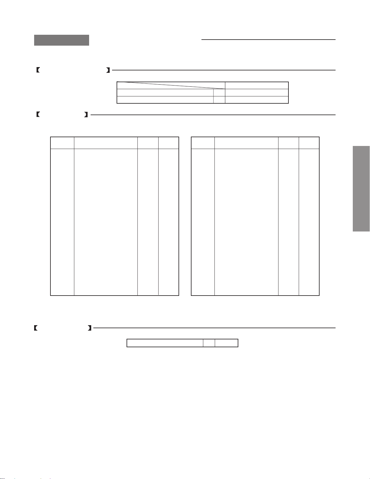
ADJUSTING ITEMS AND DATA IN THE SERVICE MODE:
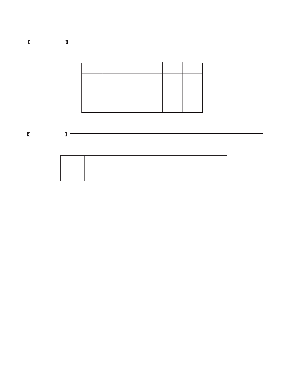
Item
HIT
VSC
WID
LIN
PARA
TRAP
DESIGN MODE
ADJUSTING ITEMS AND DATA IN THE DESIGN MODE:
Item Name of adjustment Preset Data Data
OPT1
OPT2
OPTION 1
OPTION 2
Name of adjustment Preset
V-HEIGHT
V-S CORRECTION
PICTURE WIDTH
V -LINEARITY
E-W PARABOLA(DPC)
TRAPEZIUM
Table-2
Table-3
64H
10H
28H
12H
29H
10H
80H
00H
Data
5EH
0EH
29H
11H
26H
20H
C1H
03H
– 2 –
Page 3
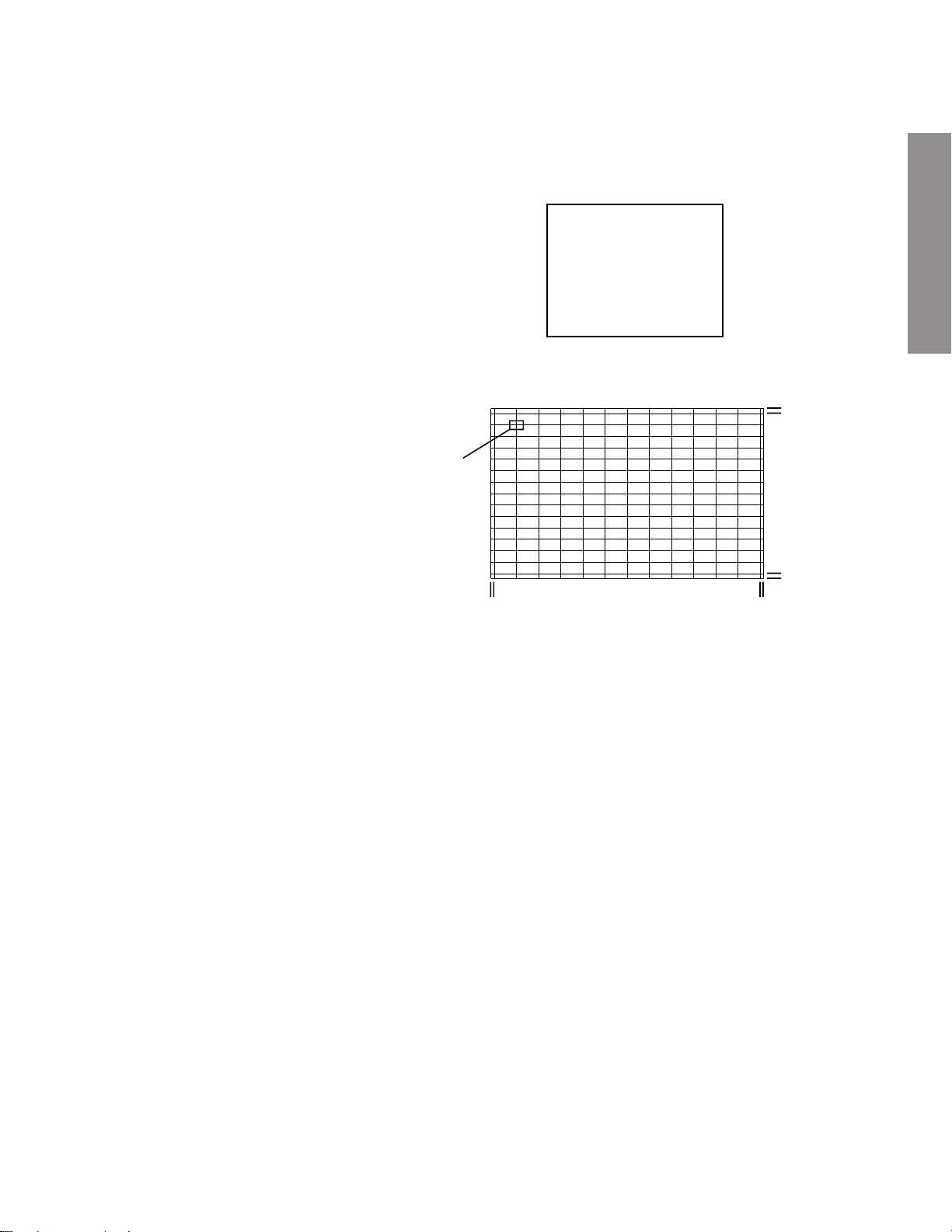
CONVERGENCE ADJUSTMENT
Adjust convergence from center to circumference in order.
1. Select the adjustment mode following the steps on page 9 of original
service manual.
KEY FUNCTION IN THE
CONVERGENCE ADJUSTMENT:
Up : 2 button
Selet Green color: 3 button
Left : 4 button
Blinking of cursor ON/OFF: 5 button
Right: 6 button
Adjust mode ON/OFF: 7 button
Down: 8 button
Erase Green line: 0 button
Erase Red line: 100 button
Erase Blue line: CHRTN (ENT) button
2. Press “7” button to display the built-in cross-hatch pattern.
RCUT
40H
21.5 (43")
26.5 (50")
28.5 (55")
31.0 (61")
Cursor
P = 43.7 x14 (43")
50.5 x14 (50")
55.8 x14 (55")
62 x14 (61")
Note:
Adjusting procedure in replacing convergence board.
1. User convergence center check. Make
sure the best convergence setting is
about the center of adjustable range.
2. CENTERING ADJUSTMENT
3. PICTURE POSITION ADJUSTMENT
4. HIT, WID ADJUSTMENT
5. CONVERGENCE ADJUSTMENT
21.5 (43")
3.5 (43", 50")
4.0 (55")
5.0 (61")
P = 72.2 x12 (43")
84 x12 (50")
92.5 x12 (55")
102.5 x12 (61")
3.5 (43", 50")
4.0 (55")
5.0 (61")
26.5 (50")
28.5 (55")
31.0 (61")
The pattern includes three colors (R, G, B).
The cursor should be blinking in Red.
This means that the Red color is adjustable.
Adjustment around cursor can be done.
3. Press “3” button to select Green color to be adjusted.
4. Press “5” button to stop the blinking of cursor.
5. Press “2 (up)”, “8 (down)”, “4 (left)” or “6 (right)” to obtain the correct
cross-hatch pattern as above.
If necessary, the specified color line can be erased from the screen.
100 button .................. to erase Red line
0 button .................. to erase Green line
RTN (ENT) button .................. to erase Blue line
6. Press “5” button to make the cursor blinking.
7. Press “2”, “8”, “4”, “6” buttons to move the cursor to other point to be
adjusted.
8. Repeat steps 4 to 7.
9. Repeat steps 3 to 8 to adjust Red and Blue colors.
Converge the selected color line into the Green line.
10. Press “7” button to enter the adjusted states.
At this time, picture changes for about 1 second.
11. Press “7” button again to return to the normal picture.
– 3 –
Page 4
K501
K503
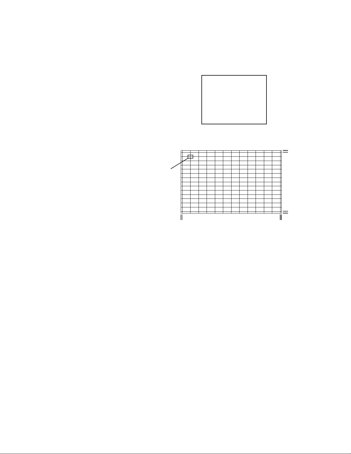
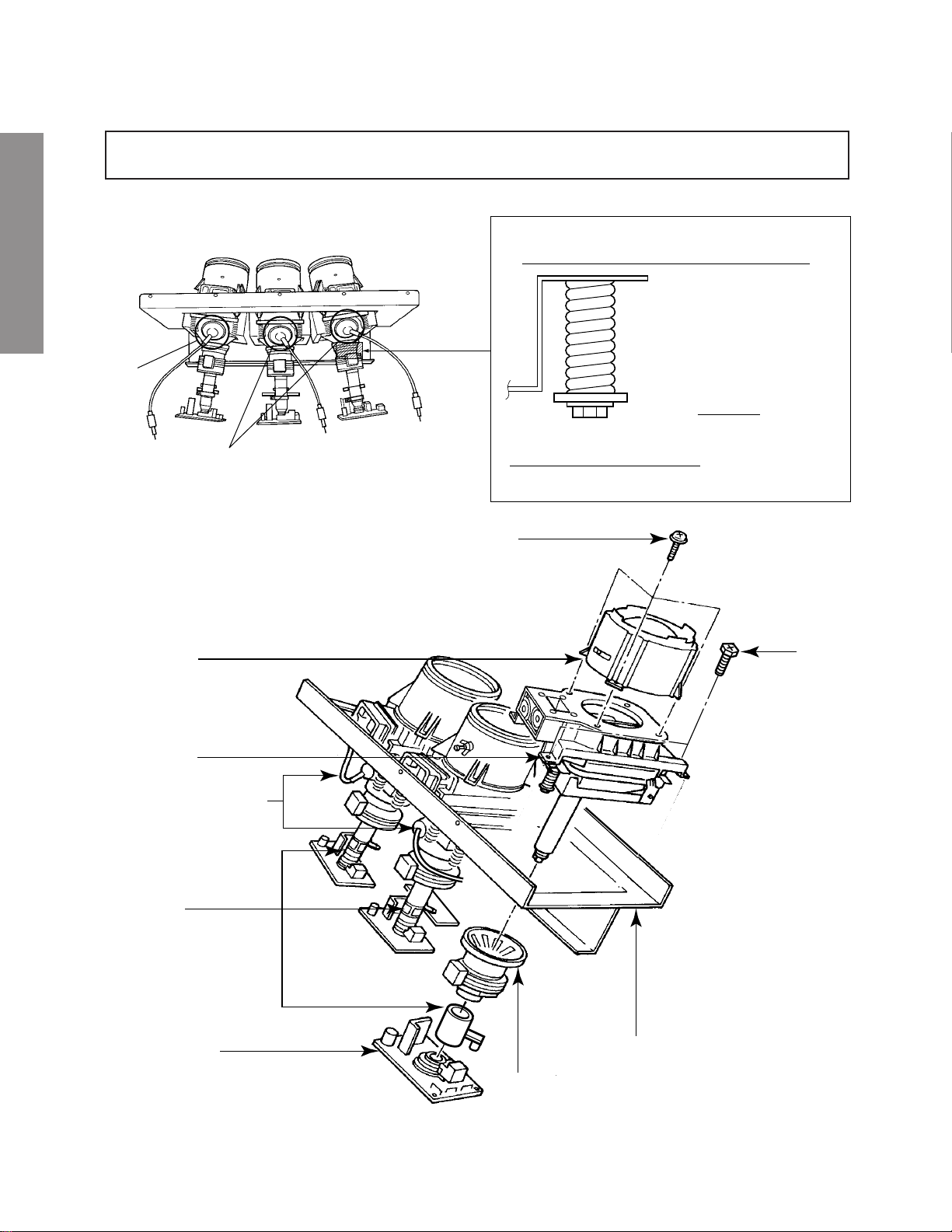
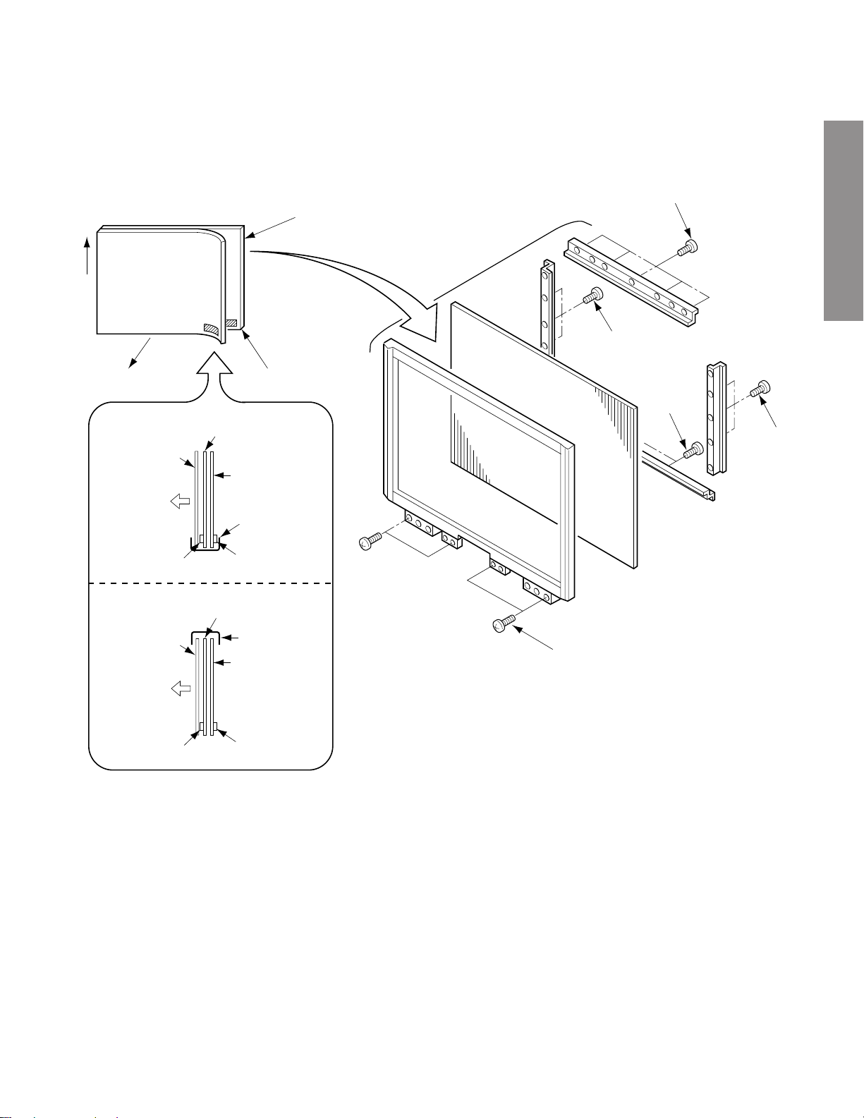
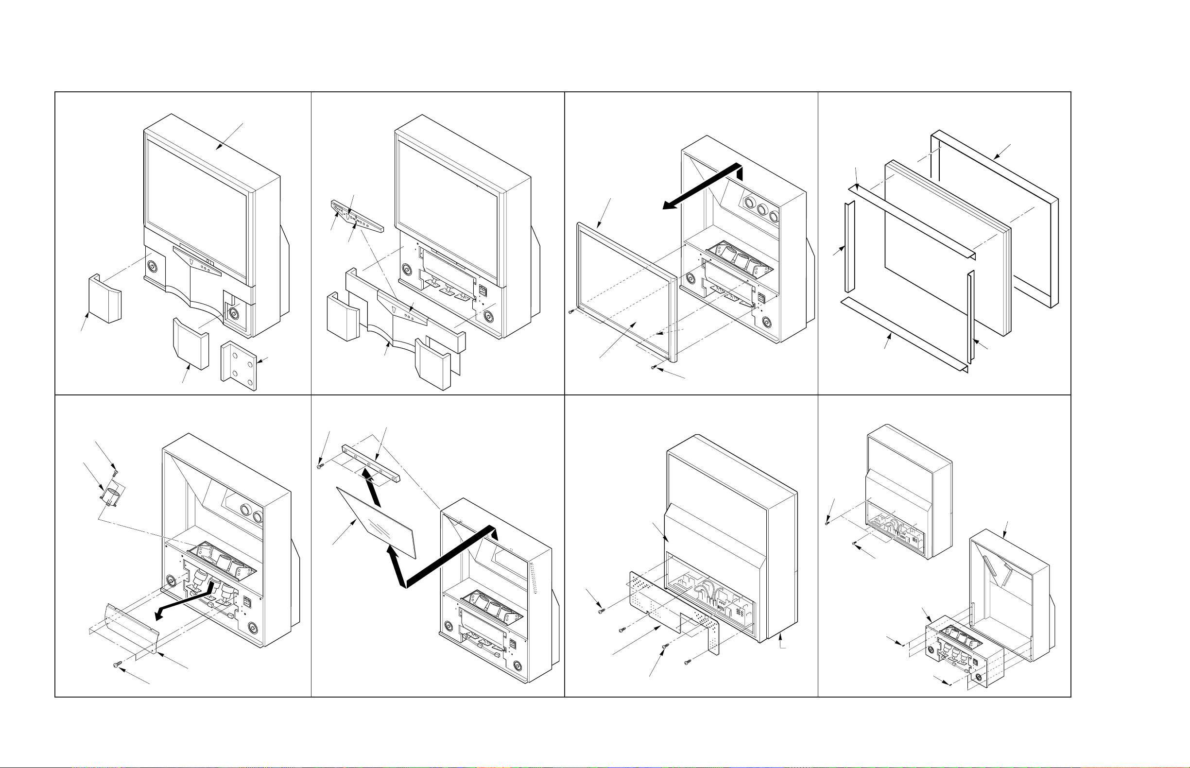
MECHANICAL DISASSEMBLY
K502
20 SCREWS
K601
LABELS
SCREWS
SCREWS
4 SCREWS
A103
A202
A102
A201
A251
A254
(A257) (A258)
11 SCREWS
9 SCREWS
A420
A424
4 SCREWS
A101
K111
K112
K113
6 SCREWS
– 4 –
Page 5

REPLACEMENT PARTS LIST DIFFERENCES
Location
No.
A101 23465852 Wood Cabinet
A102 23519892 Speaker Grille, R (43A10)
A102 23527147 Speaker Grille, R (43AX60)
A103 23519893 Speaker Grille, L (43A10)
A103 23527148 Speaker Grille, L (43AX60)
A201 23510392 Bezel (43A10)
A201 23540142 Bezel (43AX60)
A202 23450265 Control Panel (43A10)
A202 23450274 Control Panel (43AX60)
A251 23427384 Door (43A10)
A251 23427844 Door (43AX60)
A254 23445157 Knob, Power (43A10)
A254 23445424 Knob, Power (43AX60)
A255 23564376 Label
A257 23836492 Spring
A258 23451976 Push Catch
A420 23427355 Back Cover
A424 23540128 Back Board
A701 23525619 Case (43A10)
A701 23525654 Case (43AX60)
A703 23935778 Packing, Top
A708 23935779 Packing, Bottom
C477 24082943 PF, 3600pF, ±3%, 1500V
C621 24085960 EL, 4.7?F, ±20%, 50V,
C636 24085960 EL, 4.7?F, ±20%, 50V,
C646 24815223 Chip, 0.022?F, ±10%
C647 24815473 Chip, 0.047?F, ±10%
C648 24815333 Chip, 0.033?F, ±10%
C664 24669479 EL, 4.7?F, ±20%, 50V
CV10 24794100 EL, 10?F, ±20%, 16V
CV11 24232103 CD, 0.01?F, +80%, _20%, 50V
CV12 24232103 CD, 0.01?F, +80%, _20%, 50V
CZ01 24797478 EL, 0.47?F, ±20%, 50V
CZ02 24794101 EL, 100?F, ±20%, 16V (43A10)
CZ03 24092398 CD, 0.01?F, +80%, _20%, 25V
CZ04 24476103 CD, 0.01?F, ±30%, 16V
CZ05 24476103 CD, 0.01?F, ±30%, 16V
CZ06 24476103 CD, 0.01?F, ±30%, 16V
CZ07 24794101 EL, 100?F, ±20%, 16V (43A10)
CZ09 24567103 PF, 0.01?F (43A10)
CZ11 24567103 PF, 0.01?F (43A10)
CZ12 24474181 Chip, 180pF, ±10% (43A10)
CZ13 24476103 CD, 0.01?F, ±30%, 16V
CZ14 24476103 CD, 0.01?F, ±30%, 16V
CZ15 24473560 CD, 56pF (43A10)
CZ16 24473470 CD, 47pF (43A10)
CZ18 24092398 CD, 0.01?F, +80%, _20%, 25V
CZ19 24794330 EL, 33?F, ±20%, 16V (43A10)
CZ23 24092398 CD, 0.01?F, +80%, _20%, 25V
CZ27 24436080 CD, 8pF, ±0.25pF (43A10)
Part No. Description
Non-Polar (43A10)
Non-Polar (43A10)
(43A10)
(43A10)
(43A10)
(43A10)
(43A10)
(43A10)
(43A10)
(43A10)
(43A10)
Location
No.
CZ28 24436151 CD, 150pF, ±0.25pF (43A10)
CZ29 24436151 CD, 150pF, ±0.25pF (43A10)
CZ30 24436101 CD, 10pF, ±0.25pF (43A10)
DB11 23358501 Diode (LED), SCL003URC5F
DB14 23118859 Diode, 1SS133
E031Z CRT-D/R Board, PB9454C1
*
E031Z CRT-D/R Board, PB9454F1
*
E032Z CRT-D/G Board, PB9454C2
*
E032Z CRT-D/G Board, PB9454F2
*
E033Z CRT-D/B Board, PB9454C3
*
E033Z CRT-D/B Board, PB9454F3
*
E034Z FRONT-CON Board, PB9454C8
*
E034Z FRONT-CON Board, PB9454F8
*
E035Z FRONT-IN Board, PB9454C9
*
E035Z FRONT-IN Board, PB9454F9
*
E036Z SVM Board, PB9454C6
*
E036Z SVM Board, PB9454F6
*
E037Z 2L-COMB Board, PB9454C7
*
E040Z REM Board, PB9454C10
*
E040Z REM Board, PB9454F10
*
K111 23430512 Delta, 67-A/B Assembly
K112 23430512 Delta, 67-A/B Assembly
K113 23430512 Delta, 67-A/B Assembly
K501 23430786 Lenti Sheet, SCREEN43KK-L
K502 23837526 Fresnel Sheet, SCREEN43KH-F
K503 23430776 CONT-SCR43DK
K601 23430514 Mirror, MIRROR43H (43A10)
K601 23430601 Mirror, MIRROR43J (43AX60)
K912 23306359 Remote Hand Unit, CT-90037
K912 23306370 Remote Hand Unit, CT-90047
K912A 23101998 Battery, R6KGT SP-2T (43A10)
L407 23248196 Coil, Choke, TLN3457AD
LV19 23238705 Coil, Peaking, TRF4560AJ
LZ01 23289330 Coil, Peaking, TRF4330AF
LZ02 23103880 Coil (Ferrite Bead), TEM2011Y
LZ03 23289339 Coil, Peaking, TRF43R3AF
LZ04 23103880 Coil (Ferrite Bead), TEM2011Y
LZ05 23289100 Coil, Peaking, TRF4100AF
Part No. Description
(43A10)
(43AX60)
(43A10)
(43AX60)
(43A10)
(43AX60)
(43A10)
(43AX60)
(43A10)
(43AX60)
(43A10)
(43AX60)
(43A10)
(43A10)
(43AX60)
(43A10)
(43AX60)
(43A10)
(43A10)
(43A10)
(43A10)
(43A10)
– 5 –
Page 6

Location
No.
Part No. Description
Location
No.
Part No. Description
LZ06 23289270 Coil, Peaking, TRF4270AF
LZ08 23289159 Coil, Peaking, TRF41R5AF
LZ09 23289339 Coil, Peaking, TRF43R3AF
PB21 23368580 Plug, 6P
PV04 23365819 Jack, 1S3P
PV59 23367069 Plug, 9P
PZ01 23368006 Plug, 8P (43A10)
PZ02 23902064 Socket, 8P (43A10)
QA01 23000443 IC, MN102L35GFC (43AX60)
QB11 23114528 Transistor, 2SC1740S-Q
QZ01 23906207 IC, TC90A45P (43A10)
QZ02 23114528 Transistor, 2SC1740S-Q
QZ03 23114528 Transistor, 2SC1740S-Q
QZ04 23114528 Transistor, 2SC1740S-Q
R416 24533102 FR, 1k ohm, 2W
R435 24322278 MF, 0.27 ohm, 1W (43AX60)
R601 24872682 Chip, 6800 ohm, 1/16W
R602 24872682 Chip, 6800 ohm, 1/16W
R603 24872562 Chip, 5600 ohm, 1/16W
R604 24872562 Chip, 5600 ohm, 1/16W
R611 24872332 Chip, 3300 ohm, 1/16W
R612 24872332 Chip, 3300 ohm, 1/16W
R900 24000945 FR, 1.8 ohm, 2W (43AX60)
RA81 24366683 CF, 68k ohm
RA82 24366223 CF, 22k ohm
RA83 24366103 CF, 10k ohm
RA86 24366822 CF, 8200 ohm
RA87 24366153 CF, 15k ohm
RA88 24366273 CF, 27k ohm
RB11 24366271 CF, 270 ohm
RB14 24366103 CF, 10k ohm
RV16 24366750 CF, 75 ohm
RV17 24366750 CF, 75 ohm
RV18 24366750 CF, 75 ohm
RV19 24366332 CF, 3300 ohm
RZ01 24366101 CF, 100 ohm (43A10)
RZ02 24366221 CF, 220 ohm (43A10)
RZ03 24366102 CF, 1k ohm (43A10)
RZ04 24366102 CF, 1k ohm (43A10)
RZ05 24366821 CF, 820 ohm (43A10)
RZ08 24366102 CF, 1k ohm (43A10)
RZ09 24366221 CF, 220 ohm (43A10)
RZ10 24366101 CF, 100 ohm (43A10)
RZ11 24366680 CF, 68 ohm (43A10)
SA11 23145226 Switch, Push, 1C1P
SA12 23145226 Switch, Push, 1C1P
SA13 23145226 Switch, Push, 1C1P
SA14 23145226 Switch, Push, 1C1P
SA15 23145226 Switch, Push, 1C1P
SA16 23145226 Switch, Push, 1C1P
SA17 23145226 Switch, Push, 1C1P
SA18 23145226 Switch, Push, 1C1P
U701 23784783 DIGI-CONV Board, PB9453D
*
U801 DEF/Power Board, PB9451C
*
U801 DEF/Power Board, PB9451D
*
(43A10)
(43A10)
(43A10)
(43A10)
(43A10)
(43A10)
(43A10)
(43AX60)
U901 Signal/CON Board, PB9450E
*
U901 Signal/CON Board, PB9450H
*
UV01 A/V Board, PB9452C (43A10)
*
UV01 A/V Board, PB9452E (43AX60)
*
UY01 23148736 Module, MKMU31 (43AX60)
UZ01 23148718 Module, YMCJ31 (43AX60)
* V901R 23003591 Coupling, R43 (43A10)
* V901R 23005446 Coupling, R (43AX60)
* V902G 23005423 Coupling, G43 (43A10)
* V902G 23005447 Coupling, G (43AX60)
* V903B 23003593 Coupling, B43 (43A10)
* V903B 23005448 Coupling, B (43AX60)
W661 23351131 Speaker, SPK-1390
W662 23351131 Speaker, SPK-1390
Y101 23563954 Owner's Manual, English,
Y101 23563956 Owner's Manual, English,
Y101F 23563955 Owner's Manual, French,
Y101F 23563957 Owner's Manual, French,
Z410 23110842 Focus Pack, TPA6031
(43A10)
(43AX60)
43A10
43AX60
43A10
43AX60
(43AX60)
– 6 –
Page 7

MEMO
........................................................................................................................................
........................................................................................................................................
........................................................................................................................................
........................................................................................................................................
........................................................................................................................................
........................................................................................................................................
........................................................................................................................................
........................................................................................................................................
........................................................................................................................................
........................................................................................................................................
........................................................................................................................................
........................................................................................................................................
........................................................................................................................................
........................................................................................................................................
........................................................................................................................................
........................................................................................................................................
........................................................................................................................................
........................................................................................................................................
........................................................................................................................................
........................................................................................................................................
........................................................................................................................................
........................................................................................................................................
........................................................................................................................................
........................................................................................................................................
........................................................................................................................................
........................................................................................................................................
........................................................................................................................................
........................................................................................................................................
– 7 –
Page 8

TOSHIBA CORPORATION
1-1, SHIBAURA 1- CHOME, MINATO-KU, TOKYO 105-8001, JAPA N
Page 9

FILE NO. 020-200012
SERVICE MANUAL
COLOR TELEVISION
N0NSP Chassis
50A60, 50A50
(TAC0050)
55A60
(TAC0052)
(TAC0051)
,
61A60
(TAC0053)
PUBLISHED IN JAPAN, May., 2000 S
Page 10

CHAPTER 1 GENERAL ADJUSTMENTS
SAFETY INSTRUCTIONS........................................................................................................................................3
CRT ASSEMBLY REPLACEMENT AND MOUNTING ............................................................................................. 4
PICTURE TUBE COMPONENTS ADJUSTMENT.................................................................................................... 6
REPLACEMENT OF THE CRT.................................................................................................................................8
SERVICE MODE ......................................................................................................................................................9
ELECTRICAL ADJUSTMENT ................................................................................................................................11
GENERAL ADJUSTMENTSSPECIFIC INFORMATIONS
CONVERGENCE ADJUSTMENT ..........................................................................................................................13
SCREEN AND MIRROR ALIGNMENTS ................................................................................................................15
CIRCUIT CHECKS .................................................................................................................................................16
CHAPTER 2 SPECIFIC INFORMATIONS
SETTING & ADJUSTING DATA ..............................................................................................................................17
LOCATION OF CONTROLS ...................................................................................................................................18
PROGRAMMING CHANNEL MEMORY................................................................................................................. 20
CIRCUIT BLOCK DIAGRAM ..................................................................................................................................21
TABLE OF CONTENTS
MECHANICAL DISASSEMBLY ..............................................................................................................................23
CHASSIS REPLACEMENT PARTS LIST ............................................................................................................... 25
PC BOARDS BOTTOM VIEW.................................................................................................................................41
TERMINAL VIEW OF TRANSISTORS ...................................................................................................................51
SPECIFICA TIONS .................................................................................................................................................. 53
APPENDIX:
CIRCUIT DIAGRAM
– 2 –
Page 11
CHAPTER 1 GENERAL ADJUSTMENTS
SAFETY INSTRUCTIONS
WARNING: BEFORE SERVICING THIS CHASSIS, READ THE “X-RAY RADIATION PRECAUTION”, “SAFETY PRECAU-
TION” AND “PRODUCT SAFETY NOTICE” INSTRUCTIONS BELOW.
X-RAY RADIATION PRECAUTION
1. Excessive high voltage can produce potentially hazardous
X-RAY RADIATION. To avoid such hazards, the high voltage must not be above the specified limit. The nominal
value of the high voltage of this receiver is (A) kV at zero
beam current (minimum brightness) under a 120V AC
power source. The high voltage must not, under any circumstances, exceed (B) kV.
Refer to table-1 for high voltage (A), (B).
(See SETTING & ADJUSTING DATA on page 17)
Each time a receiver requires servicing, the high voltage
should be checked f ollowing the HIGH VOLT AGE CHECK
procedure in this manual. It is recommended that the reading of the high voltage be recorded as a part of the service
record. It is important to use an accurate and reliable high
voltage meter.
SAFETY PRECAUTION
WARNING : Service should not be attempted by any one unf amiliar with the necessary precautions on this receiver. The following are the necessary precautions to be observed before
servicing this chassis.
1. An isolation Transformer should be connected in the power
line between the receiver and the AC line bef ore any service is performed on the receiver.
2. Always discharge the picture tube anode to the CRT conductive coating before handling the picture tube . The picture tube is highly evacuated and if broken, glass fr agments
will be violently expelled. Use shatter proof goggles and
keep picture tube away from the unprotected body while
handling.
3. When replacing a chassis in the cabinet, always be certain that all the protective devices are put back in place,
such as; non-metallic control knobs, insulating covers,
shields, isolation resistor-capacitor network etc.
4. Before returning the set to the customer, always perform
an AC leakage current check on the exposed metallic parts
of the cabinet, such as antennas, terminals, screwheads,
metal overlays, control shafts etc. to be sure the set is saf e
to operate without danger of electrical shock. Plug the A C
line cord directly into a 120V AC outlet (do not use a line
isolation transformer during this check). Use an AC voltmeter having 5000 ohms per volt or more sensitivity in the
following manner:
PRODUCT SAFETY NOTICE
2. This receiver is equipped with a F ail Safe (FS) circuit which
prevents the receiver from producing an excessively high
voltage ev en if the B+ voltage increases abnormally. Each
time the receiver is serviced, the FS circuit must be checked
to determine that the circuit is properly functioning, following the FS CIRCUIT CHECK procedure in this manual.
3. The only source of X-RAY RADIATION in this TV receiver
is the picture tube. F or contin ued X-RAY RADIATION protection, the replacement tube must be exactly the same
type tube as specified in the parts list.
4. Some part in this receiver have special safety-related characteristics for X-RAY RADIATION protection. For continued safety, parts replacement should be undertaken only
after referring to the PRODUCT SAFETY NO TICE below.
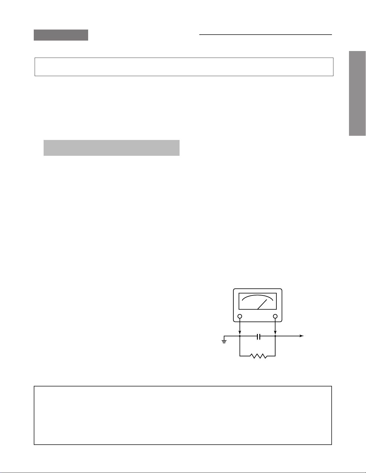
Connect a 1500 ohm 10 watt resistor , paralleled b y a 0.15
µF, AC type capacitor, between a known good earth ground
(water pipe, conduit, etc.) and the exposed metallic parts,
one at a time. Measure the AC voltage across the combination of 1500 ohm resistor and 0.15 µF capacitor. Reverse the AC plug at the AC outlet and repeat AC voltage
measurements for each exposed metallic part. Voltage
measured must not exceed 0.3 volts rms. This corresponds
to 0.2 milliamp. AC. Any value exceeding this limit constitutes a potential shock hazard and must be corrected immediately.
AC VOLTMETER
0.15µF
Place this probe on
Good earth ground
such as a water
pipe, conduit, etc.
1500 ohm
10 watt
each exposed
metallic part.
GENERAL ADJUSTMENTSSPECIFIC INFORMATIONS
Many electrical and mechanical parts in this chassis have special safety-related characteristics. These characteristics are
often passed unnoticed by a visual inspection and the protection afforded by them cannot necessarily be obtained b y using
replacement components rated for higher voltage, w attage, etc. Replacement parts which have these special saf ety characteristics are identified in this manual and its supplements; electrical components having such features are identified by the
international hazard symbols on the schematic diagram and the parts list.
Before replacing any of these components, read the parts list in this manual carefully. The use of substitute replacement
parts which do not have the same safety characteristics as specified in the parts list may create shock, fire, X-ray radiation or other hazards.
– 3 –
Page 12
CRT ASSEMBLY REPLACEMENT AND MOUNTING
CAUTION : DO NOT LOOSEN THE HEX HEAD BOLTS WITH SPRINGS (12 PCS), BECAUSE THOSE ARE FOR
SEALING OF CRT COOLANT.
GENERAL ADJUSTMENTSSPECIFIC INFORMATIONS
8 o’clock
4 o’clock
Lens Assembly
R
GB
Attention Serviceman
The Hex Head
Bolts with
Springs. (see
sketch) used on
CRT assembly,
are “NOT”
Adjustment Screws
DO NOT LOOSEN-FLUID
LEAKAGE WILL OCCUR.
4 Screws
4 Screws
CRT Assembly
CRT Anode Cap Assembly
S.V.M. Coil
CRT DRIVE Board
CRT Mounting
Deflection Yoke and Conver Yoke
Lens and Neck Components View
– 4 –
Page 13
TO REMOVE CRT (Same procedure for R, G, B)
1. Remove CRT DRIVE Board, S. V. M. COIL and
DEF. YOKE from CRT.
2. Remove Lens Assembly.
3. Detach CRT Anode Cap from CRT.
4. Remove CRT Assembly from CRT Mounting.
CRT REPLACEMENT (Same procedure for R, G, B)
Reverse the removal procedures except the followings.
1. Anode Cable should be replaced with new one.
See “SERVICING PRECAUTIONS” shown below.
2. Install silicon (T461B) to the CRT, replace the Anode
cable and put enough silicon again on around the Anode Cap as illustrated.
CAUTION: Align the Anode cable as illustrated on page
4.
ADJUSTING PROCEDURE IN REPLACING CRT
1. R.G.B. FOCUS ADJUSTMENT (page 6.)
2. PICTURE TILT ADJUSTMENT (page 6.)
3. USER CONVERGENCE CENTER CHECK
(See owner's manual.)
4. CENTERING ADJUSTMENT (page 6.)
5. CONVERGENCE ADJUSTMENT (page 13.)
6. WHITE BALANCE ADJUSTMENT (page 12.)
Adjustments are complete.
Anode Cap
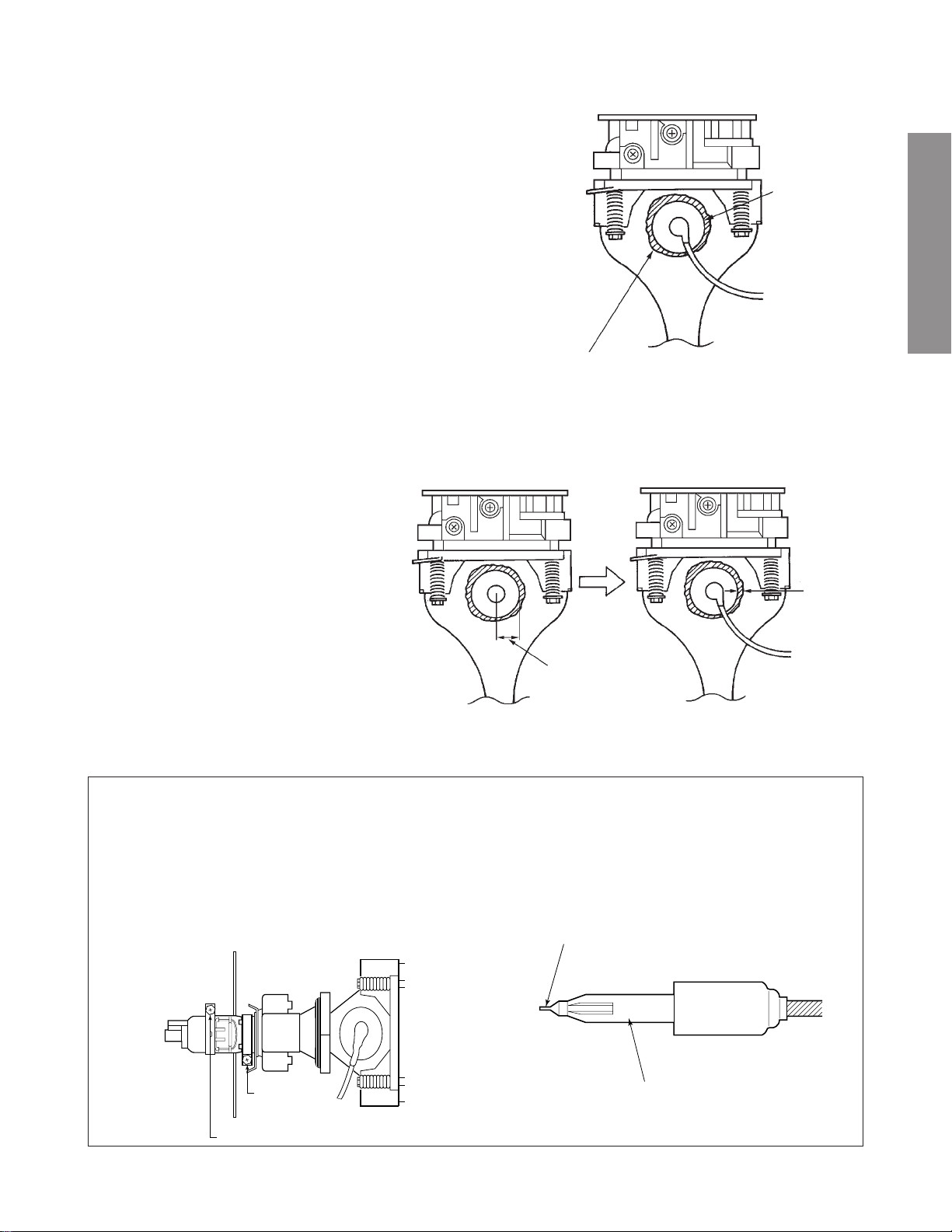
GENERAL ADJUSTMENTSSPECIFIC INFORMATIONS
Silicon
(On shaded area)
TSE3843W #23960136
SERVICING PRECAUTIONS
■ Do not use a magnetized screw driver for screws
of Deflection Yoke and Velocity Modulation Coil to
avoid magnetization of electron gun.
Magnetization of electron gun will degrade basic
function and result in unbalance of right and left
shift of user static convergence, and result in no
variable quantity.
2 ~ 5 mm
15 ~ 25 mm
■ When replacing the anode cap assembly (CRT) or
anode lead assembly (F.B.T.), remove the anode
lead holder from old one and attach the holder
again to new anode lead.
■ Check the point of anode lead in a straight
line, if it is winding, please revise it.
Screw for
D.Y
Screw for SVM coil
Anode lead holder
– 5 –
Page 14
WARNING : BEFORE SERVICING THIS CHASSIS , READ THE “X-RAY RADIA TION PRECA UTION”, “SAFETY PRECAUTION” AND “PRODUCT SAFETY NOTICE” ON PAGE 3 OF THIS MANUAL.
DESCRIPTION OF NECK COMPONENTS TILT ADJUSTMENT
GENERAL ADJUSTMENTSSPECIFIC INFORMATIONS
1 Deflection yoke and convergence yoke
The position on the neck is required most front
(CRT funnel side) and the screw is fastened after
rotating yoke adjusting picture tilt.
2 Centering magnet
After adjusting picture tilt, picture position is finally
fixed by this magnet.
In order to get maximum margin of user convergence control for center of screen, this magnet
have to be used for center convergence adjustment.
PICTURE TUBE COMPONENTS ADJUSTMENT
2
1
Rotate R, G, B deflection yoke so that picture becomes
horizon, then fasten screw.
CENTERING ADJUSTMENT
1. Stretch a thread between two center slots of screen
edge (top and bottom, left and right).
2. Select the adjustment mode.
3. Press TV/VIDEO button on the Remote Control to display the white cross-bar.
PREPARATION
Operate the receiver for at least 5 minutes.
R, G, B FOCUS ADJUSTMENT
1. Before adjusting the R, G, B FOCUS, remove the 4
screws of Lens Assembly which is fixed on the CRT
Assembly. (See page 4.)
Then turn around the Lens Assembly by 180˚ to adjust
the fastening screw (Fig. a) and f asten the 4 scre ws to
secure Lens Assembly.
2. Select the adjustment mode. (See page 9.)
3. Press “7” button to display the built-in cross-hatch.
4. Press “0” and “R TN” buttons to mak e the picture a single Red color.
100 button ............... to erase Red color
0 button ............... to erase Green color
RTN button ............... to erase Blue color
5. Loosen the fasten screw and adjust Red lense focus
to best focusing point of picture center. Then fasten
the screw. (See Fig. a.)
4. Perform VCEN adjustment. (See page 11.)
5. Adjust G centering magnet so that the cross-bar pattern center comes to screen center.
6. Perform HEIGHT adjustment . (See page 12.)
7. Perform VERT. LINEARITY adjustment.
8. Perform WIDTH adjustment. (See page 12.)
9. Check whole quality of green line.
10
. Adjust R, B centering magnet so that the cross-bar pat-
tern center comes to screen center.
Fig. a
6. Adjust FOCUS VR “R” of FOCUS PACK to find best
focusing point of picture center.
7. Repeat steps 3 to 5 for Green and Blue colors.
– 6 –
Page 15
LOCATION OF SCREEN AND FOCUS VR’S
RGB
SCREEN VR
GENERAL ADJUSTMENTSSPECIFIC INFORMATIONS
FOCUS VR
– 7 –
Page 16
Service parts are provided for each R, G and B.
The contents of the parts are as follows.
HITACHI
CRT
GENERAL ADJUSTMENTSSPECIFIC INFORMATIONS
REPLACEMENT OF THE CRT
RGB
50A50 23796001 23005397 23796003
50A60 23005114 23005115 ↑
55A60 23005242 ↑↑
61A60 23005249 ↑ 23796486
REPLACEMENT OF HIGH VOLTAGE CABLE
ANODE LEAD
RUBBER BOOT
LEAD HOLDER
Fig. a
Z450 TP A5007
1. When replacing Anode Lead or Anode Cap with new
one, remove Lead Holder from old lead as shown in
figure below, and put it on ne w lead. Do not throw awa y
Lead Holder.
NOTE : THE LEAD HOLDER IS ATTACHED TO
TP A5007 (Z450), BUT IS NO T A TTACHED T O
ANODE LEAD AND ANODE CAP. RUBBER
BOOT IS ATTA CHED TO ANODE LEAD AND
ANODE CAP.
2. Detaching Lead Holder
RUBBER BOOT
LOCK LEAD HOLDER
Fig. b
Cut here rubber boot
and lead together to
detach Lead Holder.
OLD
ANODE LEAD
or
ANODE CAP
– 8 –
Page 17
1. ENTERING TO SERVICE MODE
1) Press MUTE button once
on Remote Control.
MUTE
SERVICE MODE
2) Press MUTE button
again to keep pressing.
3) While pressing the MUTE button,
press MENU button on TV set.
S
(Service mode display)
2. DISPLAYING THE ADJUSTMENT MENU
1) Press MENU button on TV.
Service mode
S
Press
Press
Adjustment mode
3. KEY FUNCTION IN THE SERVICE MODE
The following key entry during display of adjustment menu provides special functions.
Screen adjustment mode ON/OFF: TV (ANT)/VIDEO button (on TV)
Selection of the adjustment items : Channel s/t (on TV or Remote)
Change of the data value : Volume s/t (on TV or Remote)
Adjustment menu mode ON/OFF : MENU button (on TV)
Initialization of the memory (QA02) : RECALL+Channel button on TV (s)
Initialization of the self diagnostic data: RECALL+Channel button on TV (t)
“RCUT” selection : 1 button
“GCUT” selection : 2 button
“BCUT” selection : 3 button
“SCNT” selection : 4 button
“SCOL” selection : 5 button
“TNTC” selection : 6 button
Convergence adj : 7 button
Test audio signal ON/OFF (1kHz) : 8 button
Self diagnostic display : 9 button
GENERAL ADJUSTMENTSSPECIFIC INFORMATIONS
Item
Data
– 9 –
Page 18
4. SELECTING THE ADJUSTING ITEMS
1) Every pressing of CHANNEL s button in the service mode changes the adjustment items in the order of table-2.
(t button for reverse order)
Refer to table-2 for preset data of adjustment mode.
(See SETTING & ADJUSTING DATA on page 17)
5. ADJUSTING THE DATA
1) Pressing of VOLUME s or t button will cahnge the value of data in the range from 00H to FFH. The variable range
depends on the adjusting item.
6. EXIT FROM SERVICE MODE
1) Pressing POWER button to turn off the TV once.
■ INITIALIZATION OF MEMORY DATA OF QA02
GENERAL ADJUSTMENTSSPECIFIC INFORMATIONS
After replacing QA02, the following initialization is required.
1. Enter the service mode, then select any register item.
2. Press and hold the RECALL button on the Remote, then press the CHANNEL s button on the TV . The initialization of QA02
has been complated.
3. Check the picture carefully. If necessary, adjust any adjustment item above.
Perform “Programming Channel Memory” on the owner's manual.
CAUTION: Never attempt to initialize the data unless QA02 has been replaced.
7. SELF DIAGNOSTIC FUNCTION
1) Press “9” button on Remote Control during display of adjustment menu in the service mode.
The diagnosis will begin to check if interface among IC’s are executed properly.
2) During diagnosis, the following displays are shown.
SELF CHECK
1
2
3
4
5
1 Part number of microprocessor (QA01)
2 Operation number of protection circuit (current limiter) . . . . “000” is normal.
3 BUS line check “OK” ................... Normal
4 BUS line ACK (acknowledge) check
5 Sync. signal check Green display..... Normal
NO. 23XXXXXX
POWER : 000
BUS LINE : OK
BUS CONT : OK
BLOCK : MAIN SUB
“SCL-GND” or “NG” ........... SCL-GND short circuit
“SDA-GND” or “NG” ........... SDA-GND short circuit
“SCL-SDA” or “NG” ............ SCL-SDA short circuit
“OK” ..................... Normal
Display of Location Number . . . . NG
(Display example)
“QA02 NG”, “H001 NG”, “Q501 NG” etc.
Note: The indication of failure place is only one place though failure places are plural. When
repair of a failure place finishes, the next failure place is indicated. (The order of priority of
indication is left side.)
Red display ........ NG
MAIN ........ Main sync
SUB .......... Sub sync (when turn on the PIP)
– 10 –
Page 19
ELECTRICAL ADJUSTMENT
ITEM ADJUSTMENT PROCEDURE
VERTICAL POSITION (VCEN)
SUB-BRIGHTNESS
(BRTC)
SUB-COLOR
(SCOL)
SUB-TINT
(TNTC)
1. Call up the adjustment mode display, then select item VCEN.
2. Press the VOLUME s or t button to get the voltage +30 ±10 mV.
3. Measuring method of voltage as follows.
TP-V
(on SIGNAL board)
TP-G C
(on SIGNAL board)
DIGITAL
VOLT METER
1. Constrict the picture height until the
vertical retrace line appears adjusting
the HEIGHT control on the MAIN board.
2. Adjust the CONTRAST to the minimum
and BRIGHTNESS to the center.
3. Enter the service mode, then select
“BRTC” register.
4. Adjust the data value so the belt of
vertical retrace line just disappear.
5. Adjust the HEIGHT control.
* Adjust the SUB-BRIGHTENESS after
adjusting the WHITE BALANCE.
Vertical retrace line
1. Receive color-bar signal from color-bar generator.
2. Adjust the BRIGHTNESS and CONTRAST to the center (RESET status).
3. Connect oscilloscope to TP501on the MAIN board.
4. Enter the service mode, then select “SCOL”.
5. Temporarily adjust the data value to
achieve about 1V0-p of blue bar.
6. Select “TNTC” register.
Magenta
Blue
7. Adjust the data value to obtain the blue
bar to magenta bar ratio of 3:2 as
shown.
0
2
8. Select “SCOL” register.
9. Adjust the data value to achieve 1.8V
of blue bar on scope.
0-p
10. Check the picture with off-air signal.
3 (1.8V
0-P
GENERAL ADJUSTMENTSSPECIFIC INFORMATIONS
)
SUB-CONTRAST
(SCNT)
1. Tune in a color program and adjust the BRIGHTNESS and CONTRAST to
normal mode(RESET).
2. Enter the service mode, then select "SCNT" register.
3. Change "SCNT" data to13H.
4. Check the picture contrast.
PICTURE POSITION 1. Receive the pattern signal which shows it's center
on the screen.
2. Adjust the picture position alternately by turning
CENTERING MAGNETS for proper picture position.
3. Check the picture with off-air signal.
– 11 –
Page 20
ITEM ADJUSTMENT PROCEDURE
HEIGHT
(HIT)
WIDTH
(WID)
GENERAL ADJUSTMENTSSPECIFIC INFORMATIONS
VERTICAL LINEARITY
(VLIN)
WHITE BALANCE
(RCUT)
(GCUT)
(BCUT)
(RDRV)
(BDRV)
1. Call up the adjustment mode display, then select the item HIT.
2. Press the VOLUME s or t button to get the picture so the top of raster begins
to lack.
3. Press the VOLUME s button to advance the data by 10 steps.
Note : Check the vertical picture position is correct.
1. Call up the adjustment mode display, then select the item WID.
2. Press the VOLUME s or t button to get the picture so the left and right edges
of raster begins to lack.
3. Press the VOLUME s or t button to advance the data by 10 steps.
Note : Check the horizontal picture position is correct.
1. Call up the adjustment mode display, then select the item VLIN.
2. Receive cross-hatch pattern signal.
3. Press the VOLUME s or t
button to obtain the picture of
the best linearity.
4. Then readjust the item HIT.
Center
1. Press RESET button on TV or remote hand set.
2. Call up the adjustment mode display, then adjust the data of items RCUT, GCUT
and BCUT to “40”.
3. Press TV (ANT)/VIDEO button on TV.
4. Gradually rotate R, G and B SCREEN volume of FOCUS PAC (page 7) clockwise or counterclockwise until the raster appears slightly on the CRT through
the each lens, and leave them.
(Look into the lens in order to check the raster.)
5. Press TV (ANT)/VIDEO button on TV again.
6. Exit from service mode.
7. Receive white laster pattern signal, and adjust the contrast to the minimum to
make white picture to low light.
8. Adjust the data of items RCUT, GCUT and BCUT for low light area.
9. Adjust the contrast to the maximum to make white picture to high light.
10. Adjust the data of items GDRV and BDRV Controls for proper white-balanced
picture in high light area.
11. Check the white balance in both low and high light areas. If necessary, perform
again steps from 7 to 9.
The data of item GDRV changes red drive actually.
*
– 12 –
Page 21
CONVERGENCE ADJUSTMENT
Adjust convergence from center to circumference in order.
1. Select the adjustment mode following the steps on page 9.
KEY FUNCTION IN THE
CONVERGENCE ADJUSTMENT:
RCUT
40H
Up : 2 button
Selet Green color: 3 button
Left : 4 button
Blinking of cursor ON/OFF: 5 button
Right: 6 button
Adjust mode ON/OFF: 7 button
Down: 8 button
Erase Green line: 0 button
Erase Red line: 100 button
Erase Blue line: CHRTN (ENT) button
Note:
Adjusting procedure in replacing convergence board.
1. User convergence center check. Make
sure the best convergence setting is
about the center of adjustable range.
2. CENTERING ADJUSTMENT
3. PICTURE POSITION ADJUSTMENT
4. HIT, WID ADJUSTMENT
5. CONVERGENCE ADJUSTMENT
2. Press “7” button to display the built-in cross-hatch pattern.
27.5
Cursor
P = 50.5 x14 (50")
55.8 x14 (55")
62 x14 (61")
27.5
44
P = 84 x12 (50")
92 x12 (55")
103 x12 (61")
The pattern includes three colors (R, G, B).
The cursor should be blinking in Red.
This means that the Red color is adjustable.
Adjustment around cursor can be done.
3. Press “3” button to select Green color to be adjusted.
4. Press “5” button to stop the blinking of cursor.
5. Press “2 (up)”, “8 (down)”, “4 (left)” or “6 (right)” to obtain the correct
cross-hatch pattern as above.
If necessary, the specified color line can be erased from the screen.
100 button .................. to erase Red line
0 button .................. to erase Green line
RTN (ENT) button .................. to erase Blue line
6. Press “5” button to make the cursor blinking.
7. Press “2”, “8”, “4”, “6” buttons to move the cursor to other point to be
adjusted.
8. Repeat steps 4 to 7.
9. Repeat steps 3 to 8 to adjust Red and Blue colors.
Converge the selected color line into the Green line.
10. Press “7” button to enter the adjusted states.
At this time, picture changes for about 1 second.
11. Press “7” button again to return to the normal picture.
GENERAL ADJUSTMENTSSPECIFIC INFORMATIONS
– 13 –
Page 22

NOTES
In many cases, color misconv ergence may be corrected by returning HIT and WID data in main deflection side to initial adjusting
values. Following cases will surely require readjustment of convergence.
CRT REPLACEMENT
When CRT is replaced, main deflection readjustment and color matching are required.
Perform following procedures.
1. Replace two CRT’s of blue and red.
2. Perform horizontal adjustment for blue and red yokes on base of green CRT data. Mount yoke and velocity mod. coil alignment, pushing towards CRT without gap.
3. Adjust alignment of blue and red. (Refer Alignment adjustment for details.)
4. Rotating centering magnet, adjust CRT centers of red and blue to CRT center of green.
(Picture position adjustment)
GENERAL ADJUSTMENTSSPECIFIC INFORMATIONS
5. Adjust HIT and WID data of main deflection, and decide data at the most precise screen comparing to green data.
6. Adjust convergence of each screen picture for color matching. Do not move green one at this time.
7. After convergence adjustment of each screen picture finishes, replace green CRT.
For green CRT as well, repeat steps 2 to 5 above on bases of red and blue color matching to adjust convergence.
REPLACING CONVERGENCE UNIT
When replacing convergence unit, all picture screens require readjustment basically, but the following method allo ws process be
reduced considerably.
1. Replace the memory (Q713) on defective unit with memory on new unit. Mounting the unit on the SET after the above
working realizes picture screen before replacement immediately.
2. Mount unit which has combination of old and new memories, on SET and turn it on. Screen shows whole picture looks like
straightly shifted towards vertical or horizontal direction.
3. Adjust again centers of green, red and blue with centering magnets.
4. Check each picture screen for slight disparity of color and picture size. If necessary, add some adjustments of main deflection and color matching of convergence.
– 14 –
Page 23
SCREEN AND MIRROR ALIGNMENTS
ASSEMBLING OF
FRONT SCREEN
FRONT
Protect shield
FRONT
Label with part
number
(for 50”)
Lenticular sheet
MOUNTING OF
FRONT SCREEN
5 screws
Fresnel sheet
GENERAL ADJUSTMENTSSPECIFIC INFORMATIONS
3 screws
Protect shield
3 screws
3 screws
Fresnel sheet
Stick cotton
cloth tape
Label with part
number
(for 55”, 61”)
Lenticular sheet
Protect shield
FRONT
Label with part
number
Stick contton
cloth tape
Fresnel sheet
Label with part
number
CAUTION : Do not hold the optical system parts (lens and
mirror) with bare hand to avoid finger-prints on
the surface of those parts.
HOW TO CLEAN LENS AND MIRROR
1. Be sure to remove sand dust with an air brush, etc.
2. When it is stained slightly , breathe upon it and wipe awa y
with the specified cleaning cloth.
For other stains than the above, wipe the stains away
with the specified cloth into which a cleaning liquid has
been soaked.
Cleaning liquid.................... LENS LUSTER (Manufac-
tured by Edmund Scientific
Co.), etc.
4 screws
Please refer to Mechanical Disassembly on page 23.
*
HOW TO CLEAN SCREEN
When cleaning the screen, use a soft cloth so as not to
damage the screen.
1. Wipe the screen with a dry cloth to remove moisture on
the screen.
Note : Absolutely do not use detergent, water, alcohol,
benzine, thinner, etc. for cleaning in order not to
wipe away the black print on the surface.
– 15 –
Page 24
CIRCUIT CHECKS
HIGH VOLTAGE CHECK
CAUTION: There is no HIGH VOLTAGE ADJUSTMENT on
this chassis. Checking should be done following
the steps below.
1. Connect an accurate high voltage meter to the anode of
the picture tube.
2. Turn on the receiver. Set the BRIGHTNESS and CONTRAST to minimum (zero beam current).
3. High voltage must be measured below (B) kV.
Refer to table-1 for high voltage (B).
(See SETTING & ADJUSTING DATA on page 17)
GENERAL ADJUSTMENTSSPECIFIC INFORMATIONS
4. Vary the BRIGHTNESS to both extremes to be sure the
high voltage does not exceed the limit under any conditions.
CAUTION:
When the following parts fail, check the High Voltage after
replacing.
Location
No.
T461
C447
C406
C407
ANODE VOLTAGE MEASURING METHOD
CAUTION: Take extra precaution when measuring this high
1. Disconnect the FBT anode cable as outlined below . Measure high voltage at the point where the cable enters the
FBT.
2. Holding the rubber cover firmly, turn it counterclockwise
and check that the lock has been disengaged. (See Fig. b
on page 8.)
3. Determine the extent of the rubber cover before disconnecting the cable.
4. Pull straight up the anode cable to disconnect.
5. When reconnecting the cable, proceed in the reverse order .
After reconnecting, tug on the cable to check that it is secure.
Name
Flyback Trans.
Capacitor
Capacitor
Capacitor
voltage. High voltages are also present in
surrounding circuit boards (CRT DRIVE assembly, DEFLECTION assembly, and POWER
SUPPLY assembly).
Name
TFB3078ZD
3900pF, ±3%
1500pF, ±3%
4700pF, ±3%
FS CIRCUIT CHECK
The Fail Safe (FS) circuit check is indispensable for the final
check in servicing. Checking should be done following the
steps below.
1. Turn the receiver on.
2. T emporarily short TP- (R) and TP- (X) on the DEF/POWER
Board with a jumper wire.
Raster and sound will disappear.
3. The receiver must remain in this state ev en after removing
the jumper wire. This is the evidence that the FS circuit is
functioning properly.
4. To obtain a picture again, temporarily turn the receiver off
and allow the FS circuit more than 5 seconds to reset. Then
turn the receiver on to produce a normal picture.
Troubleshooting Guide for Fail Safe Circuit
Check that the set returns to normal operation when
pin 12 of Z801 is grounded with jumper wire.
YES NO
Check the voltage across
Capacitor C471 is
approximately (
Refer to table –4 for
fall safe voltage (
YES
Defective Fail Safe Circuit
C)
volts.
C)
(See SETTING & ADJUSTING
DATA on page17)
.
NO
Faulty power
circuit or horizontal circuit.
– 16 –
Page 25
CHAPTER 2 SPECIFIC INFORMATIONS
SETTING & ADJUSTING DATA
SAFETY INSTRUCTIONS
HIGH VOLTAGE AT ZERO BEAM: (A) 31.3 kV
MAX HIGH VOLTAGE:
Table-1
SERVICE MODE
43", 50", 55", 61"
(B) 32.4 kV
ADJUSTING ITEMS AND DATA IN THE SERVICE MODE:
Item Name of adjustment
RCUT
GCUT
BCUT
GDRV
BDRV
CNTX
BRTC
COLC
TNTC
SCOL
SCNT
HPOS
VPOS
HIT
LIN
VSC
WID
VPS
R CUTOFF
G CUTOFF
B CUTOFF
G DRIVE
B DRIVE
SUB CONT MAX
SUB-BRIGHT
SUB-COLOR
SUB-TINT
SUB COLOR
SUB-CONTRAST
HORIZ. POSITION
VERT. POSITION
HEIGHT
V-LINEARITY
V-S CORRECTION
PICTURE WIDTH
V -SHIFT
Preset Date
40H
40H
40H
40H
40H
7FH
80H
50H
44H
05H
10H
19H
00H
64H
12H
10H
28H
18H
←
←
←
←
←
←
←
←
←
←
←
←
←
←
←
←
23H
←
Item Name of adjustment Preset Date
VCP
PARA
CNR
TRAP
HCP
VFC
PHUE
PCNT
PCOL
RGBB
PROF
PBOF
PGOF
STRH
STRP
VLD
VCEN
TVOP
V-COMPENSATE
E-W PARABOLA (DPC)
E-W CORNER
TRAPEZIUM
H-COMPENSATE
V-F CORRECT
PIP TINT
PIP CONT
PIP COLOR
RGB BRIGHT
PIP R OFFSET
PIP B OFFSET
PIP YG OFFSET
START H
START PTN
VLD
V POSITION
TV OPTION
0AH
29H
08H
10H
00H
00H
00H
00H
0FH
54H
00H
00H
00H
67H
8AH
41H
81H
00H
GENERAL ADJUSTMENTSSPECIFIC INFORMATIONS
←
←
←
←
←
←
←
←
←
←
←
←
←
←
←
←
←
←
CIRCUIT CHECKS
T able-2
FBT DETECTION VOLTAGE (C) 24.5V
Table-3
– 17 –
Page 26
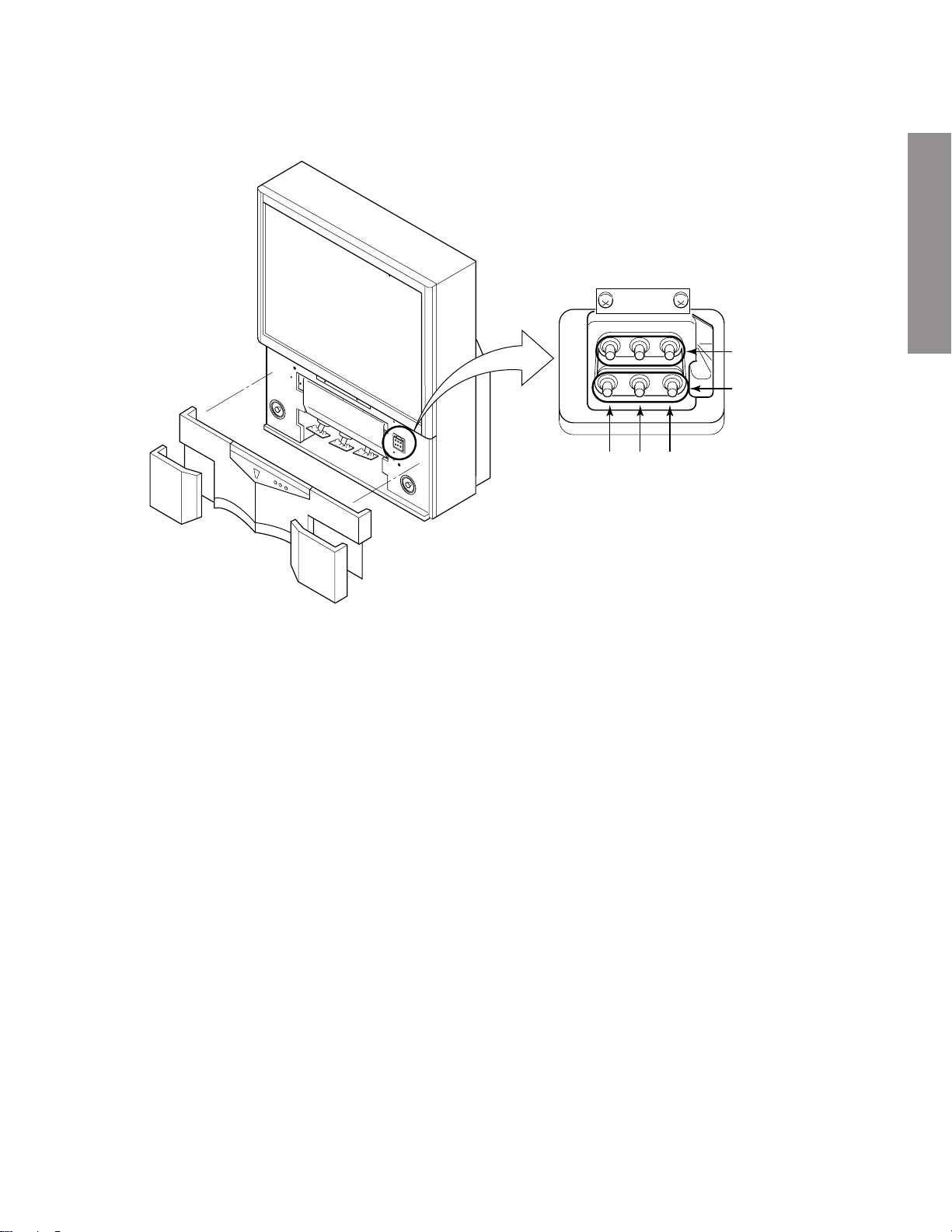
TV front
GENERAL ADJUSTMENTSSPECIFIC INFORMATIONS
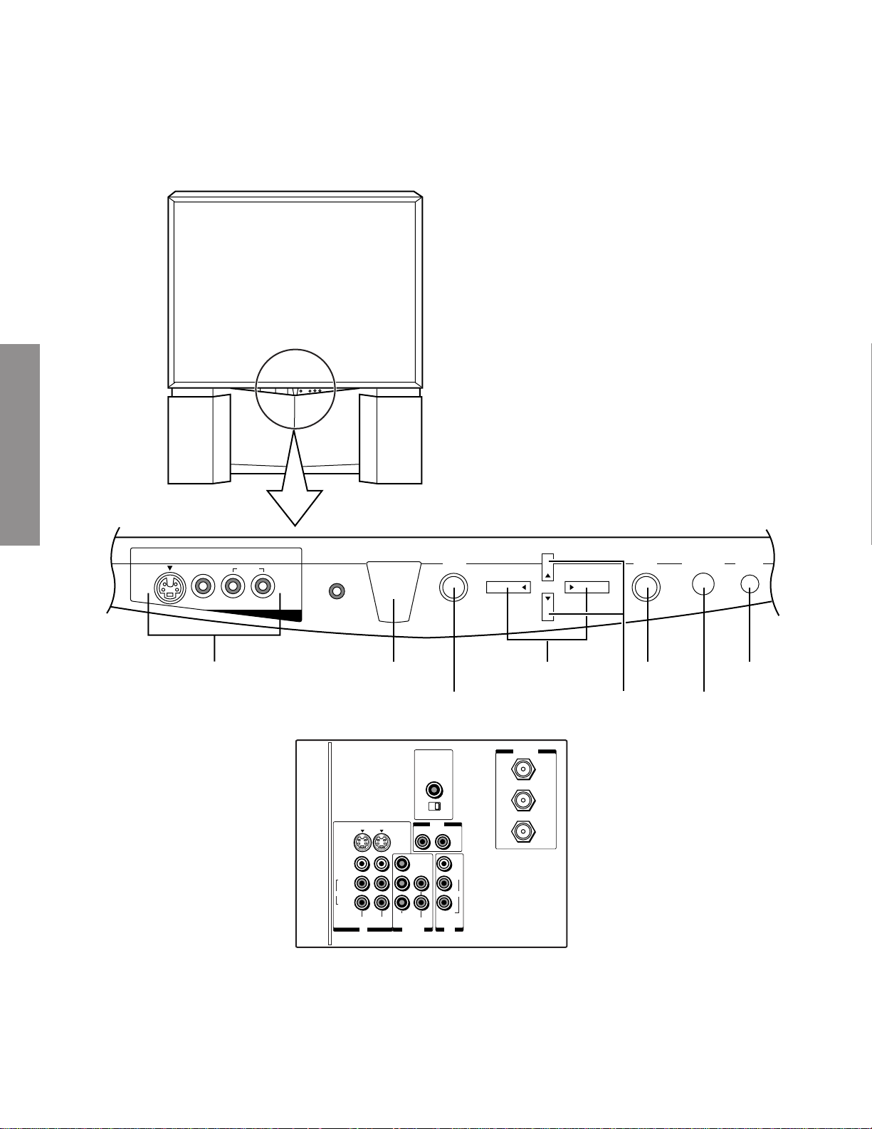
LOCATION OF CONTROLS (Representative : 50A60)
S-VIDEO
TV rear
Behind the door
AUDIO
VIDEO L/MONO
Video Audio inputs
MENU
VOL VOL
CH
EXIT DEMOTV/VIDEO
POWER
R
POWER
MENU
AUDIO CENTER
CHANNEL IN
ON OFF
OUT
R
L
S-VIDEO
VIDEO
L/
MONO
AUDIO
R
COLOR
VIDEO-2VIDEO-1
STREAM
INPUT
VAR
AUDIO
Y
VIDEO
L/
C
B
MONO
AUDIO
RLR
C
R
AUDIO
OUTDVD ININ
CH
VOLUMET S
ANT (75Ω)
ANT-1
OUT
ANT-2
EXIT DEMO
CHANNEL st
TV/VIDEO
– 18 –
Page 27
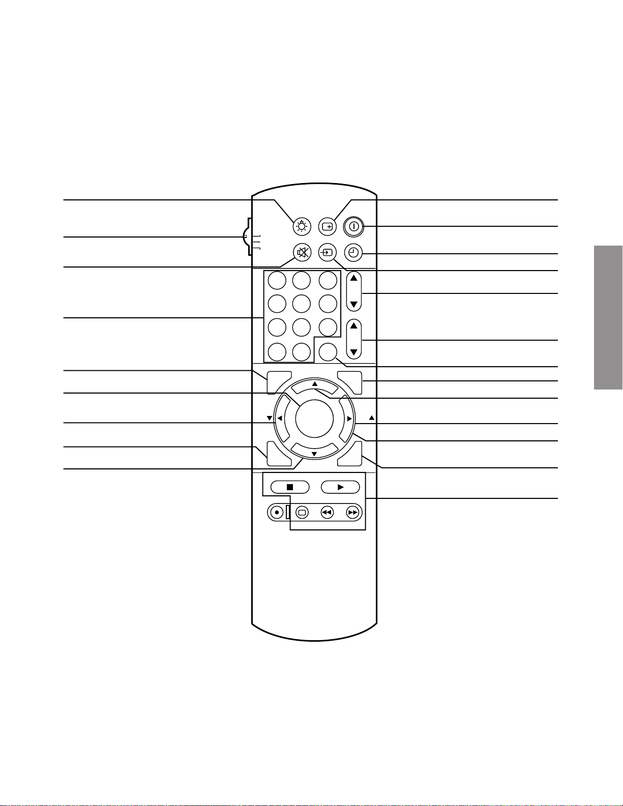
Remote Control
LIGHT
TV/CABLE/VCR switch
Set to “TV” to control the TV.
MUTE
Channel Number
C. CAPT
ENTER
FAV t
RESET
PIP CH t
TV
CABLE
VCR
1
4
7
100
C.CAPT
FAV
RESET
STOP SOURCE
REC
RECALL
3
6
9
CH RTN
ENT
PLAY PIP
POWER
TIMER
CH
VOL
MENU
EXIT
LIGHT
MUTE TV/VIDEO
2
5
8
0
ADV/
PIP CH
ENTER
ADV/
PIP CH
TV/VCR REW FF
FAV
RECALL
POWER
TIMER
TV/VIDEO
CHANNEL s/t
VOLUME s/t
CH RTN
MENU
PIP CH
s
FAV s
s/t/T/S
EXIT
PIP functions
(For “TV” and “CABLE” modes)
GENERAL ADJUSTMENTSSPECIFIC INFORMATIONS
STILL LOCATE SWAP
– 19 –
Page 28

PROGRAMMING CHANNEL MEMORY
The channel memory is the list of TV channel numbers the TV tunes in when you press the CHANNEL s or t button.
First, use the TV/CABLE and CH PROGRAM functions to preset all active channels in your area automatically.
If necessary, arrange the preset channels with the ADD/ERASE functions so that you can tune into only desired channels.
Note: If you utilize both ANT-1 and ANT-2 terminals for some model, perform programming channels for each input source.
TV/CABLE function
1 Press MENU, then press S or T until the SET UP menu
appears.
GENERAL ADJUSTMENTSSPECIFIC INFORMATIONS
2 Press t (or s) until “TV/CABLE” is highlighted.
3 Press : or ; to highlight either “TV” or “CABLE”, whichever
you use.
CH PROGRAM function
1 Select “CH PROGRAM” following steps 1 and 2 above.
2 Press : or ; to start channel programming.
The TV will automatically cycle through all the TV or
CABLE channels selected by the TV/CABLE function, and
store active channels in the channel memory.
3 When channel programming is complete, you will see the
message to the right appears.
4 Press CHANNEL s or t to make sure the channel
programming has been done properly.
ADD/ERASE function
After performing the CH PROGRAM function, you can add or
erase specific channels.
1 Select the channel you want to erase using the CHANNEL
s or t button, or select the channel you want to add using
the Channel Number buttons.
2 Press MENU, then press S or T until the SET UP menu
appears.
3 Press t (or s) until “ADD/ERASE” is highlighted.
4 Press S or T :
To erase the channel press the button until “ERASE” is
highlighted.
To add the channel press the button until “ADD” is
highlighted.
5 Repeat steps 1 to 4 for other channels.
You have now completed the channel programming.
Note: The CHANNEL t/s buttons on the TV function as the
t/s buttons while a menu is on the screen.
* Please refer to owner's manual in detail.
– 20 –
Page 29
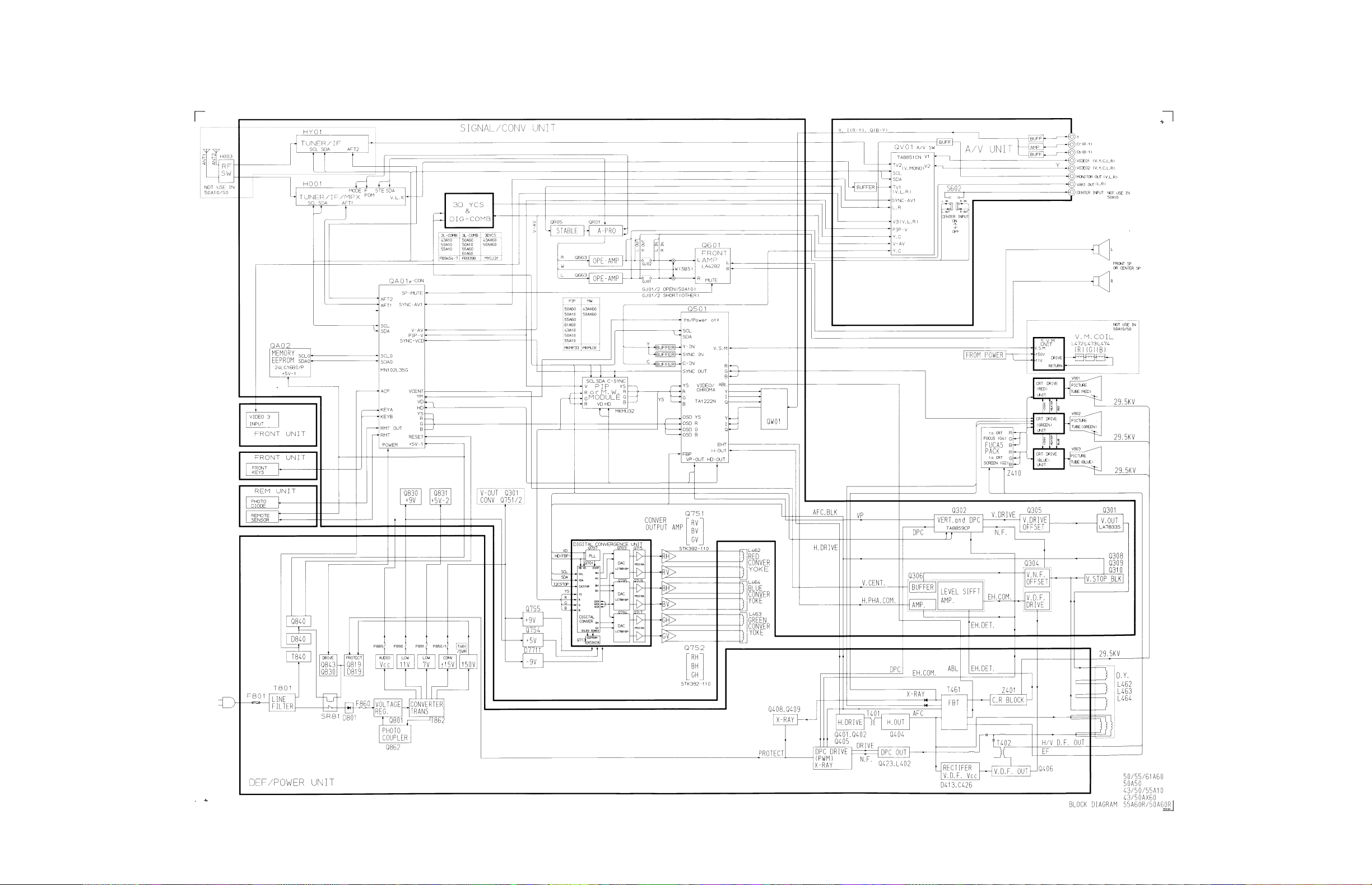
CIRCUIT BLOCK DIAGRAM
– 21 –
– 22 –
Page 30
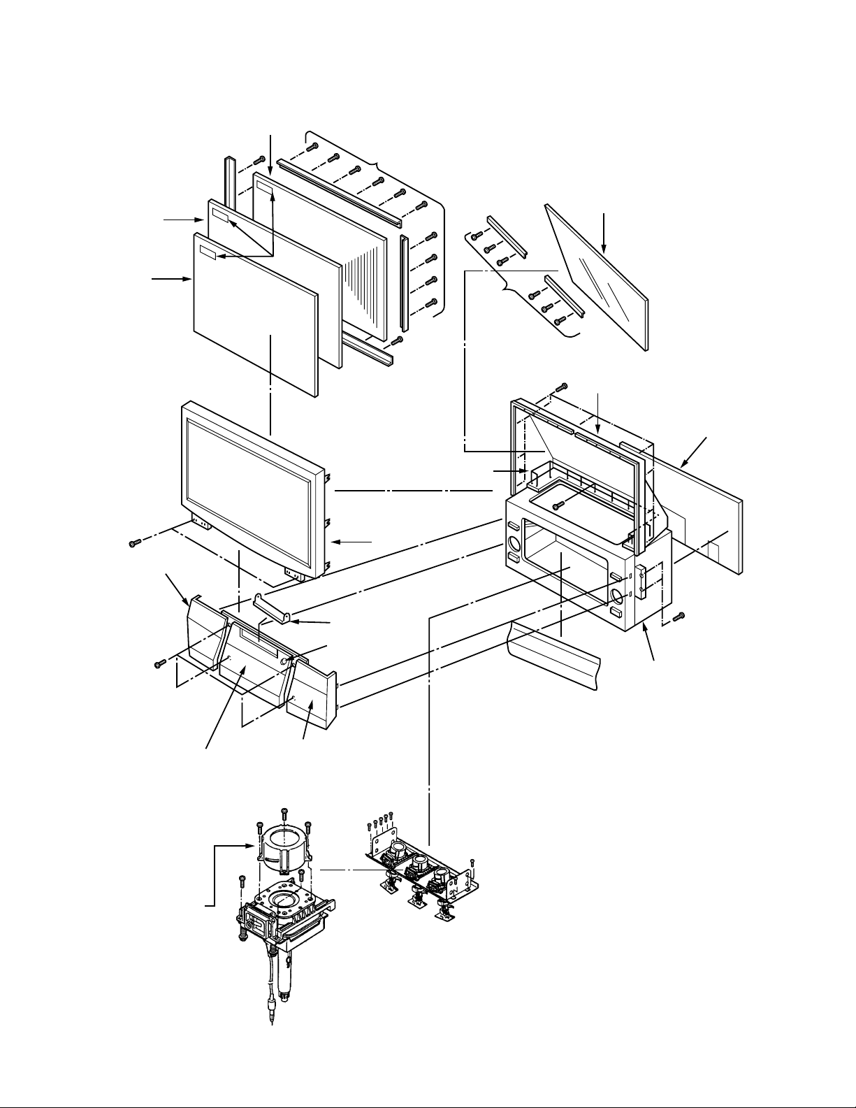
MECHANICAL DISASSEMBLY
K501
(K511)
4 screws
A201
K502
A424
A160
3 screws
5 screws
A401
3 screws
3 screws
3 screws
(A150)
(A110)
1 screw
A265
A266
A266
A267
A201
1 Speaker Grille Removal 2 Control Panel Removal
A101
A221
(A322)
A213
A224
A202
A103
A126
A127
A268
3 Front Mask Removal
4 Mask Removal
A102
5 Shield Plate, Lens Removal 6 Mirror Removal
4 screws
K111
K112
K113
4 screws
A269
5 screws
K601
– 23 –
A152
7 Back Board Removal
8 Light Box Removal
– 24 –
Page 31

CHASSIS REPLACEMENT PARTS LIST
WARNING: BEFORE SER VICING THIS CHASSIS, READ THE “X-RA Y RADIATION PRECAUTION”, “SAFETY PRE-
CAUTION” AND “PRODUCT SAFETY NOTICE” ON PAGE 3 OF THIS MANUAL.
CAUTION: The international hazard symbols “ ” in the schematic diag r am and the parts list designate components
which have special characteristics important for safety and should be replaced only with types identical to those in the
original circuit or specified in the parts list. The mounting position of replacements is to be identical with originals.
Before replacing any of these components, read carefully the PRODUCT SAFETY NOTICE. Do not degrade the
safety of the receiver through improper servicing.
NOTICE:
•
The part number must be used when ordering parts, in order to assist in processing, be sure to include the Model
number and Description.
•
The PC board assembly with * mark is no longer available after the end of the production.
Models : 50A60/50A50/55A60/61A60
Capacitors ............. CD : Ceramic Disk PF : Plastic Film EL : Electrolytic
Resistors ............... CF : Carbon Film CC : Carbon Composition MF : Metal Film
OMF : Oxide Metal Film VR : Variable Resistor FR : Fusible Resistor
(All CD and PF capacitors are ±5%, 50V and all resistors, ±5%, 1/6W unless otherwise noted.)
GENERAL ADJUSTMENTSSPECIFIC INFORMATIONS
Location
No.
CAPACITORSCAPACITORS
CAPACITORS
CAPACITORSCAPACITORS
C102 24665221 EL, 220?F, ±20%, 10V
C105 24815102 Chip, 0.001?F, ±10%
C106 24669479 EL, 4.7?F, ±20%, 50V
C107 24666221 EL, 220?F, ±20%, 16V
C112 24665221 EL, 220?F, ±20%, 10V
C115 24815102 Chip, 0.001?F, ±10%
C117 24666221 EL, 220?F, ±20%, 16V
C151 24815102 Chip, 0.001?F, ±10%
C201 24666100 EL, 10?F, ±20%, 16V
C203 24092178 Chip, 0.1?F, ±10%, 25V
C204 24669010 EL, 1?F, ±20%, 50V
C205 24206229 EL, 2.2?F, ±20%, 50V
C206 24666100 EL, 10?F, ±20%, 16V
C207 24781390 Chip, 39pF, SL
C208 24781390 Chip, 39pF, SL
C209 24781390 Chip, 39pF, SL
C212 24666100 EL, 10?F, ±20%, 16V
C213 24092616 Chip, 0.33?F, ±10%, 16V
C220 24709100 EL, 10?F, ±20%, 200V
C301 24815683 Chip, 0.068?F, ±10%
C302 24092463 Chip, 0.22?F, ±10%, 16V
C303 24666101 EL, 100?F, ±20%, 16V
C304 24092178 Chip, 0.1?F, ±10%, 25V
C305 24815103 Chip, 0.01?F, ±10%
C306 24815102 Chip, 0.001?F, ±10%
C307 24617912 EL, 2.2?F, ±10%, 50V
C309 24815102 Chip, 0.001?F, ±10%
C311 24815103 Chip, 0.01?F, ±10%
C312 24815102 Chip, 0.001?F, ±10%
C313 24092573 Chip, 0.47?F, ±10%, 16V
C314 24092178 Chip, 0.1?F, ±10%, 25V
C315 24666222 EL, 2200?F, ±20%, 16V
C316 24666101 EL, 100?F, ±20%, 16V
C317 24815222 Chip, 0.0022?F, ±10%
C318 24815182 Chip, 0.0018?F, ±10%
C319 24667101 EL, 100?F, ±20%, 25V
Part No. Description
(50A60/55A60/61A60)
(50A60/55A60/61A60)
(50A60/55A60/61A60)
(50A60/55A60/61A60)
Location
No.
C320 24667101 EL, 100?F, ±20%, 25V
C321 24667101 EL, 100?F, ±20%, 25V
C322 24815393 Chip, 0.039?F, ±10%
C323 24815563 Chip, 0.056?F, ±10%
C324 24669101 EL, 100?F, ±20%, 50V
C325 24082057 PF, 0.22?F, 100V
C326 24092463 Chip, 0.22?F, ±10%, 16V
C327 24092463 Chip, 0.22?F, ±10%, 16V
C328 24082260 PF, 4700pF, 100V
C329 24669100 EL, 10?F, ±20%, 50V
C330 24085946 EL, 10?F, ±20%, 16V,
C331 24815333 Chip, 0.033?F, ±10%
C332 24669221 EL, 220?F, ±20%, 50V
C333 24693473 PF, 0.047?F, 100V
C334 24591471 PF, 470pF
C335 24092178 Chip, 0.1?F, ±10%, 25V
C336 24815472 Chip, 0.0047?F, ±10%
C340 24092463 Chip, 0.22?F, ±10%, 16V
C350 24669229 EL, 2.2?F, ±20%, 50V
C351 24092178 Chip, 0.1?F, ±10%, 25V
C352 24669229 EL, 2.2?F, ±20%, 50V
C401 24092178 Chip, 0.1?F, ±10%, 25V
C401 24214821 CD, 820pF, ±10%, 500V
C402 24214391 CD, 390pF, ±10%, 500V
C402 24815223 Chip, 0.022?F, ±10%
C403 24678100 EL, 10?F, ±20%, 200V
C404 24212152 CD, 1500pF, ±10%
C404 24669229 EL, 2.2?F, ±20%, 50V
C405 24567124 PF, 0.12?F
* C406 24082823 PF, 1500pF, ±3%, 1800V
* C407 24082946 PF, 4700pF, ±3%, 1500V
* C408 24820123 PF, 0.012?F, ±10%, 630V
C410 24095900 PF, 3.3?F, ±10%, 100V
C412 24828473 PF, 0.047?F, 200V
C413 24214221 CD, 220pF, ±10%, 500V
* C414 24095782 PF, 0.47?F, 400V
Part No. Description
(50A60/55A60/61A60)
(50A60/55A60/61A60)
Non-Polar (50A60/55A60/61A60)
(50A60/55A60/61A60)
(50A60/55A60/61A60)
– 25 –
Page 32

Location
No.
Part No. Description
Location
No.
Part No. Description
C415 24092484 CD, 1500pF, ±10%, 2kV
C416 24828333 PF, 0.033?F, 200V
C417 24679229 EL, 2.2?F, ±20%, 250V
C418 24679330 EL, 33?F, ±20%, 250V
C419 24669479 EL, 4.7?F, ±20%, 50V
C423 24640908 EL, 33?F, ±20%, 160V
C426 24211222 CD, 2200pF, ±10%, 2kV
C427 24828473 PF, 0.047?F, 200V
C429 24591102 PF, 1000pF
C430 24567103 PF, 0.01?F
GENERAL ADJUSTMENTSSPECIFIC INFORMATIONS
C431 24567103 PF, 0.01?F
C432 24567683 PF, 0.068?F
C433 24666100 EL, 10?F, ±20%, 16V
C434 24679479 EL, 4.7?F, ±20%, 250V
C435 24820222 PF, 0.0022?F, 630V
* C447 24082944 PF, 3900pF, ±3%, 1500V
* C448 24820123 PF, 0.012?F, ±10%, 630V
C450 24815103 Chip, 0.01?F, ±10%
C451 24815222 Chip, 0.0022?F, ±10%
C452 24666101 EL, 100?F, ±20%, 16V
C481 24666101 EL, 100?F, ±20%, 16V
C482 24567223 PF, 0.022?F
C484 24501102 PF, 0.001?F
C485 24567104 PF, 0.1?F
C497 24567474 PF, 0.47?F
C498 24669479 EL, 4.7?F, ±20%, 50V
C501 24815103 Chip, 0.01?F, ±10%
C502 24815103 Chip, 0.01?F, ±10%
C503 24665101 EL, 100?F, ±20%, 10V
C504 24815222 Chip, 0.0022?F, ±10%
C505 24774120 Chip, 12pF, CH
C508 24666100 EL, 10?F, ±20%, 16V
C509 24666101 EL, 100?F, ±20%, 16V
C510 24666101 EL, 100?F, ±20%, 16V
C511 24815103 Chip, 0.01?F, ±10%
C512 24206228 EL, 0.22?F, ±20%, 50V
C513 24815103 Chip, 0.01?F, ±10%
C514 24092178 Chip, 0.1?F, ±10%, 25V
C515 24092178 Chip, 0.1?F, ±10%, 25V
C517 24774010 Chip, 1pF, ±0.25pF, CH
C520 24666101 EL, 100?F, ±20%, 16V
C531 24666101 EL, 100?F, ±20%, 16V
C532 24666100 EL, 10?F, ±20%, 16V
C601 24815102 Chip, 0.001?F, ±10%
C602 24815102 Chip, 0.001?F, ±10%
C603 24669100 EL, 10?F, ±20%, 50V
C604 24669100 EL, 10?F, ±20%, 50V
C605 24667101 EL, 100?F, ±20%, 25V
C606 24667101 EL, 100?F, ±20%, 25V
C607 24567104 PF, 0.1?F
C608 24567104 PF, 0.1?F
C609 24669102 EL, 1000?F, ±20%, 50V
C610 24669102 EL, 1000?F, ±20%, 50V
C611 24667221 EL, 220?F, ±20%, 25V
C612 24666470 EL, 47?F, ±20%, 16V
C621 24206479 EL, 4.7?F, ±20%, 50V
C622 24206108 EL, 0.1?F, ±20%, 50V
C623 24814472 Chip, 0.01?F, +80%, -20%
C624 24206479 EL, 4.7?F, ±20%, 50V
C625 24206479 EL, 4.7?F, ±20%, 50V
C626 24206479 EL, 4.7?F, ±20%, 50V
C627 24206479 EL, 4.7?F, ±20%, 50V
(50A60/55A60/61A60)
(50A60/55A60/61A60)
C628 24206100 EL, 10?F, ±20%, 50V
C629 24206100 EL, 10?F, ±20%, 50V
C630 24206108 EL, 0.1?F, ±20%, 50V
C631 24814472 Chip, 0.01?F, +80%, -20%
C632 24203470 EL, 47?F, ±20%, 16V
C633 24092178 Chip, 0.1?F, ±10%, 25V
C634 24206108 EL, 0.1?F, ±20%, 50V
C635 24206479 EL, 4.7?F, ±20%, 50V
C636 24206479 EL, 4.7?F, ±20%, 50V
C637 24206100 EL, 10?F, ±20%, 50V
C638 24794101 EL, 100?F, ±20%, 16V
C639 24815103 Chip, 0.01?F, ±10%
C640 24815273 Chip, 0.027?F, ±10%
C641 24815822 Chip, 0.0082?F, ±10%
C642 24206100 EL, 10?F, ±20%, 50V
C643 24206479 EL, 4.7?F, ±20%, 50V
C644 24206339 EL, 3.3?F, ±20%, 50V
C645 24815333 Chip, 0.033?F, ±10%
C646 24815223 Chip, 0.022?F, ±10%
C647 24815473 Chip, 0.047?F, ±10%
C648 24815333 Chip, 0.033?F, ±10%
C649 24815273 Chip, 0.027?F, ±10%
C650 24815822 Chip, 0.0082?F, ±10%
C651 24815103 Chip, 0.01?F, ±10%
C652 24815103 Chip, 0.01?F, ±10%
C653 24814103 Chip, 0.01?F, +80%, -20%
C654 24763101 EL, 100?F, ±20%, 16V
C661 24206010 EL, 1?F, ±20%, 50V
C662 24206010 EL, 1?F, ±20%, 50V
C663 24206010 EL, 1?F, ±20%, 50V
C664 24669479 EL, 4.7?F, ±20%, 50V
C665 24815103 Chip, 0.01?F, ±10%
C666 24206010 EL, 1?F, ±20%, 50V
C667 24747478 EL, 0.47?F, ±20%, 50V
C680 24669471 EL, 470?F, ±20%, 50V
C681 24666100 EL, 10?F, ±20%, 16V
C682 24092178 Chip, 0.1?F, ±10%, 25V
C690 24815103 Chip, 0.01?F, ±10%
C701 24781330 Chip, 33pF, SL
C702 24781330 Chip, 33pF, SL
C703 24781330 Chip, 33pF, SL
C704 24781330 Chip, 33pF, SL
C706 24092293 Chip, 0.1?F, +80%, -20%, 25V
C708 24092293 Chip, 0.1?F, +80%, -20%, 25V
C710 24092293 Chip, 0.1?F, +80%, -20%, 25V
C711 24203100 EL, 10?F, ±20%, 16V
C712 24781330 Chip, 33pF, SL
C713 24781330 Chip, 33pF, SL
C714 24092293 Chip, 0.1?F, +80%, -20%, 25V
C717 24774470 Chip, 47pF, CH
C718 24774470 Chip, 47pF, CH
C719 24794101 EL, 100?F, ±20%, 16V
C720 24092293 Chip, 0.1?F, +80%, -20%, 25V
C721 24774070 Chip, 7pF, ±0.25pF, CH
C724 24092293 Chip, 0.1?F, +80%, -20%, 25V
C725 24092293 Chip, 0.1?F, +80%, -20%, 25V
C726 24092293 Chip, 0.1?F, +80%, -20%, 25V
C727 24092293 Chip, 0.1?F, +80%, -20%, 25V
C728 24100104 Chip, 0.1?F, +80%, -20%, 25V
C730 24092293 Chip, 0.1?F, +80%, -20%, 25V
C731 24092293 Chip, 0.1?F, +80%, -20%, 25V
C732 24815103 Chip, 0.01?F, ±10%
C735 24092178 Chip, 0.1?F, ±10%, 25V
C736 24100104 Chip, 0.1?F, +80%, -20%, 25V
– 26 –
Page 33

Location
No.
Part No. Description
Location
No.
Part No. Description
C739 24092293 Chip, 0.1?F, +80%, -20%, 25V
C740 24092293 Chip, 0.1?F, +80%, -20%, 25V
C741 24794470 EL, 47?F, ±20%, 16V
C742 24794470 EL, 47?F, ±20%, 16V
C743 24092293 Chip, 0.1?F, +80%, -20%, 25V
C744 24092293 Chip, 0.1?F, +80%, -20%, 25V
C745 24794470 EL, 47?F, ±20%, 16V
C746 24794470 EL, 47?F, ±20%, 16V
C747 24092293 Chip, 0.1?F, +80%, -20%, 25V
C748 24092293 Chip, 0.1?F, +80%, -20%, 25V
C749 24794470 EL, 47?F, ±20%, 16V
C750 24794470 EL, 47?F, ±20%, 16V
C761 24774102 Chip, 1000pF, CH
C762 24590562 PF, 5600pF
C763 24774391 Chip, 390pF, CH
C765 24774102 Chip, 1000pF, CH
C766 24590562 PF, 5600pF
C767 24774391 Chip, 390pF, CH
C769 24774102 Chip, 1000pF, CH
C770 24590562 PF, 5600pF
C771 24774391 Chip, 390pF, CH
C772 24761221 EL, 220?F, ±20%, 6.3V
C773 24774102 Chip, 1000pF, CH
C774 24590562 PF, 5600pF
C775 24774391 Chip, 390pF, CH
C777 24774102 Chip, 1000pF, CH
C778 24590562 PF, 5600pF
C779 24774391 Chip, 390pF, CH
C781 24774102 Chip, 1000pF, CH
C782 24590562 PF, 5600pF
C783 24774391 Chip, 390pF, CH
C784 24774821 Chip, 820pF, CH
C785 24774821 Chip, 820pF, CH
C786 24774821 Chip, 820pF, CH
C787 24774821 Chip, 820pF, CH
C788 24774821 Chip, 820pF, CH
C789 24774821 Chip, 820pF, CH
C790 24092293 Chip, 0.1?F, +80%, -20%, 25V
C795 24761221 EL, 220?F, ±20%, 6.3V
C798 24763101 EL, 100?F, ±20%, 16V
C799 24763101 EL, 100?F, ±20%, 16V
C801 24082001 PF, 0.47?F, AC125V
C809 24086062 EL, 1000?F, ±20%, 200V
C810 24086062 EL, 1000?F, ±20%, 200V
C814 24092597 CD, 4700pF, ±20%, AC250V
C815 24092597 CD, 4700pF, ±20%, AC250V
C816 24073081 EL, 1.0?F, ±20%, 50V
C817 24092597 CD, 4700pF, ±20%, AC250V
C819 24567684 PF, 0.68?F
C830 24567334 PF, 0.33?F
C831 24073037 EL, 47?F, ±20%, 16V
C832 24567334 PF, 0.33?F
C833 24073037 EL, 47?F, ±20%, 16V
C840 24073072 EL, 1000?F, ±20%, 35V
C842 24073001 EL, 100?F, ±20%, 6.3V
C843 24567104 PF, 0.1?F
C857 24073060 EL, 4700?F, ±20%, 25V
C858 24073060 EL, 4700?F, ±20%, 25V
C860 24214103 CD, 0.01?F, ±10%, 500V
C863 24567104 PF, 0.1?F
C864 24092474 CD, 220pF, ±10%, 2kV
C866 24567474 PF, 0.47?F
C867 24591682 PF, 6800pF
C868 24073052 EL, 47?F, ±20%, 25V
C869 24678229 EL, 2.2?F, ±20%, 200V
C870 24082890 PF, 0.082?F, 800V
C871 24092484 CD, 1500pF, ±10%, 2kV
C872 24092474 CD, 220pF, ±10%, 2kV
C873 24567224 PF, 0.22?F
C874 24212471 CD, 470pF, ±10%
C876 24567474 PF, 0.47?F
C879 24073081 EL, 1.0?F, ±20%, 50V
C884 24086939 EL, 330?F, ±20%, 200V
C890 24073096 EL, 3300?F, ±20%, 50V
C891 24082229 PF, 0.1?F, ±10%, 250V
C894 24073043 EL, 2200?F, ±20%, 16V
C895 24073043 EL, 2200?F, ±20%, 16V
C898 24212102 CD, 1000pF, ±10%
C901 24211102 CD, 1000pF, ±10%, 2kV
C902 24794100 EL, 10?F, ±20%, 16V
C903 24232103 CD, 0.01?F, +80%, -20%
C904 24436102 CD, 1000pF
C908 24214472 CD, 4700pF, ±10%, 500V
C909 24436221 CD, 220pF
C911 24211102 CD, 1000pF, ±10%, 2kV
C912 24794100 EL, 10?F, ±20%, 16V
C914 24436102 CD, 1000pF
C915 24679330 EL, 33?F, ±20%, 250V
C916 24794101 EL, 100?F, ±20%, 16V
C918 24794470 EL, 47?F, ±20%, 16V
C919 24436221 CD, 220pF
C921 24211102 CD, 1000pF, ±10%, 2kV
C922 24794100 EL, 10?F, ±20%, 16V
C923 24794470 EL, 47?F, ±20%, 16V
C924 24232103 CD, 0.01?F, +80%, -20%
C925 24794470 EL, 47?F, ±20%, 16V
C926 24436102 CD, 1000pF
C927 24436221 CD, 220pF
C928 24214472 CD, 4700pF, ±10%, 500V
C929 24794100 EL, 10?F, ±20%, 16V
C961 24666101 EL, 100?F, ±20%, 16V
C962 24203100 EL, 10?F, ±20%, 16V
C963 24232103 CD, 0.01?F, +80%, -20%
C964 24567104 PF, 0.1?F
C7721 24815102 Chip, 0.001?F, ±10%
C7722 24781101 Chip, 100pF, SL
C7724 24667101 EL, 100?F, ±20%, 25V
C7725 24667101 EL, 100?F, ±20%, 25V
C7726 24815102 Chip, 0.001?F, ±10%
C7727 24781101 Chip, 100pF, SL
C7729 24815102 Chip, 0.001?F, ±10%
C7730 24781101 Chip, 100pF, SL
C7732 24815102 Chip, 0.001?F, ±10%
C7733 24781101 Chip, 100pF, SL
C7735 24667101 EL, 100?F, ±20%, 25V
C7736 24667101 EL, 100?F, ±20%, 25V
C7737 24815102 Chip, 0.001?F, ±10%
C7738 24781101 Chip, 100pF, SL
C7740 24815102 Chip, 0.001?F, ±10%
C7741 24781101 Chip, 100pF, SL
C7744 24815103 Chip, 0.01?F, ±10%
C7747 24667101 EL, 100?F, ±20%, 25V
C7748 24567104 PF, 0.1?F
C7749 24567104 PF, 0.1?F
C7750 24667101 EL, 100?F, ±20%, 25V
C7751 24667101 EL, 100?F, ±20%, 25V
C7752 24567104 PF, 0.1?F
C7753 24567104 PF, 0.1?F
C7754 24667101 EL, 100?F, ±20%, 25V
GENERAL ADJUSTMENTSSPECIFIC INFORMATIONS
– 27 –
Page 34

Location
No.
Part No. Description
Location
No.
Part No. Description
C7755 24667101 EL, 100?F, ±20%, 25V
C7765 24669479 EL, 4.7?F, ±20%, 50V
C7766 24669479 EL, 4.7?F, ±20%, 50V
C7767 24667470 EL, 47?F, ±20%, 25V
C7769 24815103 Chip, 0.01?F, ±10%
C7774 24781101 Chip, 100pF, SL
C7776 24667470 EL, 47?F, ±20%, 25V
CA10 24781101 Chip, 100pF, SL
CA13 24815221 Chip, 220pF, ±10%
CA18 24666470 EL, 47?F, ±20%, 16V
CA20 24774181 Chip, 180pF, CH
CA21 24092442 Chip, 0.47?F,
GENERAL ADJUSTMENTSSPECIFIC INFORMATIONS
CA22 24815103 Chip, 0.01?F, ±10%
CA23 24774181 Chip, 180pF, CH
CA24 24092442 Chip, 0.47?F,
CA25 24666100 EL, 10?F, ±20%, 16V
CA26 24092441 Chip, 1?F, +80%, -20%, 16V
CA27 24092441 Chip, 1?F, +80%, -20%, 16V
CA29 24815221 Chip, 220pF, ±10%
CA30 24774101 Chip, 100pF, CH
CA34 24781101 Chip, 100pF, SL
CA45 24666100 EL, 10?F, ±20%, 16V
CA49 24666100 EL, 10?F, ±20%, 16V
CA50 24814103 Chip, 0.01?F, +80%, -20%
CA52 24815272 Chip, 0.0027?F, ±10%
CA54 24781101 Chip, 100pF, SL
CA59 24781101 Chip, 100pF, SL
CA60 24781101 Chip, 100pF, SL
CA61 24666220 EL, 22?F, ±20%, 16V
CA64 24814103 Chip, 0.01?F, +80%, -20%
CA68 24666100 EL, 10?F, ±20%, 16V
CA69 24814103 Chip, 0.01?F, +80%, -20%
CA71 24781101 Chip, 100pF, SL
CA72 24085981 EL, 10?F, ±20%, 16V,
CA73 24666100 EL, 10?F, ±20%, 16V
CB11 24794470 EL, 47?F, ±20%, 16V
CB13 24085981 EL, 10?F, ±20%, 16V,
CB14 24781101 Chip, 100pF, SL
CB15 24794100 EL, 10?F, ±20%, 16V
CB42 24232103 CD, 0.01?F, +80%, -20%
CB61 24781221 Chip, 220pF, SL
CB90 24815103 Chip, 0.01?F, ±10%
CB91 24666100 EL, 10?F, ±20%, 16V
CD02 24591562 PF, 5600pF
CD03 24591393 PF, 0.039?F
CD04 24591393 PF, 0.039?F
CD08 24794100 EL, 10?F, ±20%, 16V
CD10 24436101 CD, 100pF
CD12 24436101 CD, 100pF
CD13 24797479 EL, 4.7?F, ±20%, 50V
CD14 24797229 EL, 2.2?F, ±20%, 50V
CD15 24794470 EL, 47?F, ±20%, 16V
CD16 24797229 EL, 2.2?F, ±20%, 50V
CR12 24092178 Chip, 0.1?F, ±10%, 25V
CR13 24092178 Chip, 0.1?F, ±10%, 25V
CR14 24092178 Chip, 0.1?F, ±10%, 25V
CR15 24092178 Chip, 0.1?F, ±10%, 25V
CR16 24092178 Chip, 0.1?F, ±10%, 25V
CR17 24092178 Chip, 0.1?F, ±10%, 25V
CS03 24436221 CD, 220pF
+80%, -20%, 16V
+80%, -20%, 16V
Non-Polar
Non-Polar
CS04 24206010 EL, 1?F, ±20%, 50V
CS07 24436221 CD, 220pF
CS08 24206010 EL, 1?F, ±20%, 50V
CS09 24436331 CD, 330pF
CS10 24206229 EL, 2.2?F, ±20%, 50V
CS11 24206010 EL, 1?F, ±20%, 50V
CS12 24436221 CD, 220pF
CS13 24206010 EL, 1?F, ±20%, 50V
CS14 24436221 CD, 220pF
CS15 24436331 CD, 330pF
CS16 24206229 EL, 2.2?F, ±20%, 50V
CS21 24436101 CD, 100pF
CS22 24436101 CD, 100pF
CS23 24206478 EL, 0.47?F, ±20%, 50V
CS24 24436331 CD, 330pF
CS25 24206229 EL, 2.2?F, ±20%, 50V
CS28 24436331 CD, 330pF
CS29 24436331 CD, 330pF
CS32 24203100 EL, 10?F, ±20%, 16V
CS33 24203100 EL, 10?F, ±20%, 16V
CS34 24436331 CD, 330pF
CS35 24206229 EL, 2.2?F, ±20%, 50V
CS36 24206229 EL, 2.2?F, ±20%, 50V
CS38 24206229 EL, 2.2?F, ±20%, 50V
CS41 24436331 CD, 330pF
CS42 24206229 EL, 2.2?F, ±20%, 50V
CS43 24436331 CD, 330pF
CS44 24206229 EL, 2.2?F, ±20%, 50V
CV01 24085981 EL, 10?F, ±20%, 16V,
Non-Polar
CV02 24232103 CD, 0.01?F, +80%, -20%
CV03 24203100 EL, 10?F, ±20%, 16V
CV04 24203100 EL, 10?F, ±20%, 16V
CV05 24203100 EL, 10?F, ±20%, 16V
CV08 24666471 EL, 470?F, ±20%, 16V
CV09 24666471 EL, 470?F, ±20%, 16V
CV13 24794100 EL, 10?F, ±20%, 16V
CV14 24232103 CD, 0.01?F, +80%, -20%
CV15 24232103 CD, 0.01?F, +80%, -20%
CV16 24085981 EL, 10?F, ±20%, 16V,
Non-Polar
CV17 24203100 EL, 10?F, ±20%, 16V
CV19 24232103 CD, 0.01?F, +80%, -20%
CV21 24203100 EL, 10?F, ±20%, 16V
CV22 24203100 EL, 10?F, ±20%, 16V
CV23 24232103 CD, 0.01?F, +80%, -20%
CV24 24232103 CD, 0.01?F, +80%, -20%
CV27 24202221 EL, 220?F, ±20%, 10V
CV28 24202221 EL, 220?F, ±20%, 10V
CV29 24203101 EL, 100?F, ±20%, 16V
CV30 24232103 CD, 0.01?F, +80%, -20%
CV31 24203100 EL, 10?F, ±20%, 16V
CV38 24203101 EL, 100?F, ±20%, 16V
CV39 24212102 CD, 1000pF, ±10%
CV40 24763101 EL, 100?F, ±20%, 16V
CV41 24232103 CD, 0.01?F, +80%, -20%
CV42 24085971 EL, 3.3?F, ±20%, 50V,
Non-Polar
CV43 24436121 CD, 120pF
CV44 24436220 CD, 22pF
CV46 24232103 CD, 0.01?F, +80%, -20%
CV48 24763101 EL, 100?F, ±20%, 16V
CV49 24232103 CD, 0.01?F, +80%, -20%
CV61 24232103 CD, 0.01?F, +80%, -20%
– 28 –
Page 35

Location
No.
Part No. Description
Location
No.
Part No. Description
CV64 24206100 EL, 10?F, ±20%, 50V
CV65 24591122 PF, 1200pF
CV66 24436561 CD, 560pF
CV67 24591102 PF, 1000pF
CV68 24206010 EL, 1?F, ±20%, 50V
CW04 24591822 PF, 8200pF
CW05 24212103 CD, 0.01?F, ±10%
CW07 24666470 EL, 47?F, ±20%, 16V
CW08 24794101 EL, 100?F, ±20%, 16V
CW09 24815103 Chip, 0.01?F, ±10%
CW12 24666470 EL, 47?F, ±20%, 16V
CW13 24709100 EL, 10?F, ±20%, 200V
CW14 24436101 CD, 100pF
CW15 24214472 CD, 4700pF, ±10%, 500V
CW16 24436101 CD, 100pF
CW17 24214472 CD, 4700pF, ±10%, 500V
CW18 24666470 EL, 47?F, ±20%, 16V
CW19 24435560 CD, 56pF, 500V
CW20 24709100 EL, 10?F, ±20%, 200V
CW21 24666470 EL, 47?F, ±20%, 16V
CW22 24436561 CD, 560pF
CW26 24212102 CD, 1000pF, ±10%
CW52 24203100 EL, 10?F, ±20%, 16V
CW53 24203100 EL, 10?F, ±20%, 16V
CW54 24203100 EL, 10?F, ±20%, 16V
CW58 24794101 EL, 100?F, ±20%, 16V
CW59 24232103 CD, 0.01?F, +80%, -20%
CY01 24665471 EL, 470?F, ±20%, 10V
CY40 24206100 EL, 10?F, ±20%, 50V
CZ03 24092442 Chip, 0.47?F,
CZ05 24814103 Chip, 0.01?F, +80%, -20%
CZ07 24092178 Chip, 0.1?F, ±10%, 25V
CZ09 24781220 Chip, 22pF, SL
CZ10 24781100 Chip, 10pF, ±0.5pF%, SL
CZ11 24781220 Chip, 22pF, SL
CZ12 24814103 Chip, 0.01?F, +80%, -20%
CZ13 24814103 Chip, 0.01?F, +80%, -20%
CZ14 24203100 EL, 10?F, ±20%, 16V
CZ17 24814103 Chip, 0.01?F, +80%, -20%
CZ19 24781181 Chip, 180pF, SL
CZ20 24814103 Chip, 0.01?F, +80%, -20%
CZ21 24781122 Chip, 1200pF, SL
CZ22 24203100 EL, 10?F, ±20%, 16V
CZ23 24814103 Chip, 0.01?F, +80%, -20%
CZ24 24814103 Chip, 0.01?F, +80%, -20%
CZ25 24203100 EL, 10?F, ±20%, 16V
CZ26 24814103 Chip, 0.01?F, +80%, -20%
CZ28 24814103 Chip, 0.01?F, +80%, -20%
CZ29 24814103 Chip, 0.01?F, +80%, -20%
CZ30 24203100 EL, 10?F, ±20%, 16V
CZ31 24092178 Chip, 0.1?F, ±10%, 25V
CZ32 24781150 Chip, 15pF, SL
CZ33 24781390 Chip, 39pF, SL
CZ34 24781150 Chip, 15pF, SL
CZ35 24781390 Chip, 39pF, SL
CZ37 24203100 EL, 10?F, ±20%, 16V
CZ38 24203100 EL, 10?F, ±20%, 16V
CZ41 24781470 Chip, 47pF, SL
CZ42 24781470 Chip, 47pF, SL
CZ45 24781100 Chip, 10pF, ±0.5pF%, SL
RESISTORSRESISTORS
RESISTORS
RESISTORSRESISTORS
R101 24383223 OMF, 22k ohm, 2W
+80%, -20%, 16V
R150 24872101 Chip, 100 ohm, 1/16W
(50A60/55A60/61A60)
R151 24872562 Chip, 5600 ohm, 1/16W
(50A60/55A60/61A60)
R152 24872103 Chip, 10k ohm, 1/16W
(50A60/55A60/61A60)
R201 24872821 Chip, 820 ohm, 1/16W
R202 24872102 Chip, 1k ohm, 1/16W
R204 24872104 Chip, 100k ohm, 1/16W
R205 24872101 Chip, 100 ohm, 1/16W
(50A60/55A60/61A60)
R206 24872102 Chip, 1k ohm, 1/16W
(50A60/55A60/61A60)
R207 24872101 Chip, 100 ohm, 1/16W
R208 24872101 Chip, 100 ohm, 1/16W
R209 24872101 Chip, 100 ohm, 1/16W
R212 24872472 Chip, 4700 ohm, 1/16W
R213 24872122 Chip, 1200 ohm, 1/16W
R214 24872222 Chip, 2200 ohm, 1/16W
R216 24872103 Chip, 10k ohm, 1/16W
R223 24872102 Chip, 1k ohm, 1/16W
R241 24367103 CF, 10k ohm, ±2%
R242 24367103 CF, 10k ohm, ±2%
R243 24381563 OMF, 56k ohm, 1/2W
R266 24872102 Chip, 1k ohm, 1/16W
R267 24872821 Chip, 820 ohm, 1/16W
R268 24872102 Chip, 1k ohm, 1/16W
R269 24872102 Chip, 1k ohm, 1/16W
R270 24872682 Chip, 6800 ohm, 1/16W
R301 24872103 Chip, 10k ohm, 1/16W
R302 24872101 Chip, 100 ohm, 1/16W
R303 24872102 Chip, 1k ohm, 1/16W
R304 24872103 Chip, 10k ohm, 1/16W
R305 24872153 Chip, 15k ohm, 1/16W
R307 24872471 Chip, 470 ohm, 1/16W
R308 24872471 Chip, 470 ohm, 1/16W
R310 24872562 Chip, 5600 ohm, 1/16W
R311 24872103 Chip, 10k ohm, 1/16W
R312 24872103 Chip, 10k ohm, 1/16W
R313 24872102 Chip, 1k ohm, 1/16W
R314 24872473 Chip, 47k ohm, 1/16W
R315 24872821 Chip, 820 ohm, 1/16W
R316 24872102 Chip, 1k ohm, 1/16W
R317 24872824 Chip, 820k ohm, 1/16W
R318 24872153 Chip, 15k ohm, 1/16W
R319 24872100 Chip, 10 ohm, 1/16W
R320 24000249 MF, 47k ohm, 1/4W
R321 24872332 Chip, 3300 ohm, 1/16W
R322 24000529 MF, 6800 ohm, 1/4W
R323 24000639 MF, 22k ohm, 1/4W
R324 24872103 Chip, 10k ohm, 1/16W
R325 24872222 Chip, 2200 ohm, 1/16W
R326 24872103 Chip, 10k ohm, 1/16W
R327 24872103 Chip, 10k ohm, 1/16W
R328 24872103 Chip, 10k ohm, 1/16W
R329 24872103 Chip, 10k ohm, 1/16W
R330 24872153 Chip, 15k ohm, 1/16W
R331 24019119 MF, 30k ohm, 1/6W
R332 24000525 MF, 4.7k ohm, 1/4W
R333 24872103 Chip, 10k ohm, 1/16W
R334 24872102 Chip, 1k ohm, 1/16W
R335 24872102 Chip, 1k ohm, 1/16W
R336 24872102 Chip, 1k ohm, 1/16W
R337 24321129 MF, 1.2 ohm, 1/2W
GENERAL ADJUSTMENTSSPECIFIC INFORMATIONS
– 29 –
Page 36

Location
No.
Part No. Description
Location
No.
Part No. Description
R338 24872682 Chip, 6800 ohm, 1/16W
R339 24872393 Chip, 39k ohm, 1/16W
R340 24872824 Chip, 820k ohm, 1/16W
R341 24872273 Chip, 27k ohm, 1/16W
R342 24872153 Chip, 15k ohm, 1/16W
R343 24872102 Chip, 1k ohm, 1/16W
R344 24382271 OMF, 270 ohm, 1W
GENERAL ADJUSTMENTSSPECIFIC INFORMATIONS
R345 24322828 MF, 0.82 ohm, 1W
R346 24382391 OMF, 390 ohm, 1W
R347 24872103 Chip, 10k ohm, 1/16W
R348 24872103 Chip, 10k ohm, 1/16W
R349 24872392 Chip, 3900 ohm, 1/16W
R350 24872822 Chip, 8200 ohm, 1/16W
R351 24366472 CF, 4700 ohm
R360 24872103 Chip, 10k ohm, 1/16W
R361 24872103 Chip, 10k ohm, 1/16W
R362 24872103 Chip, 10k ohm, 1/16W
R363 24872682 Chip, 6800 ohm, 1/16W
R364 24872103 Chip, 10k ohm, 1/16W
R370 24872102 Chip, 1k ohm, 1/16W
R371 24872823 Chip, 82k ohm, 1/16W
R372 24872332 Chip, 3300 ohm, 1/16W
R373 24872823 Chip, 82k ohm, 1/16W
R374 24872104 Chip, 100k ohm, 1/16W
R375 24872153 Chip, 15k ohm, 1/16W
R376 24872333 Chip, 33k ohm, 1/16W
R378 24872222 Chip, 2200 ohm, 1/16W
R401 24366102 CF, 1k ohm
R401 24872391 Chip, 390 ohm, 1/16W
R402 24366102 CF, 1k ohm
R403 24553272 OMF, 2700 ohm, 1W
R403 24872302 Chip, 3k ohm, 1/16W
R404 24384682 OMF, 6800 ohm, 3W
R405 24552330 OMF, 33 ohm, 1/2W
R406 24382222 OMF, 2200 ohm, 1W
R406 24872223 Chip, 22k ohm, 1/16W
R407 24552100 OMF, 10 ohm, 1/2W
R407 24872103 Chip, 10k ohm, 1/16W
R408 24366101 CF, 100 ohm
R409 24555220 OMF, 22 ohm, 3W
R410 24555220 OMF, 22 ohm, 3W
R411 24383270 OMF, 27 ohm, 2W
R412 24366223 CF, 22k ohm
R413 24366332 CF, 3300 ohm
R414 24366100 CF, 10 ohm
R415 24533102 FR, 1k ohm, 2W
R418 24019292 FR, 68 ohm, 1/2W
R419 24942102 CC, 1k ohm, 1/2W
R420 24382473 OMF, 47k ohm, 1W
R421 24382104 OMF, 100k ohm, 1W
R423 24872471 Chip, 470 ohm, 1/16W
R424 24338398 MF, 0.39 ohm, 1W
R426 24000112 FR, 10 ohm, 1/4W
(50A60/55A60/61A60)
(50A60/55A60/61A60)
(50A60/55A60/61A60)
(50A60/55A60/61A60)
(50A60/55A60/61A60)
(50A60/55A60/61A60)
(50A60/55A60/61A60)
(50A60/55A60/61A60)
(50A60/55A60/61A60)
(50A60/55A60/61A60)
(50A60/55A60/61A60)
R428 24310109 MF, 1.0 ohm, 1/2W
R431 24383102 OMF, 1k ohm, 2W
(50A60/55A60/61A60)
R432 24376274 CF, 270k ohm, 1/2W
(50A60/55A60/61A60)
R432 24552101 OMF, 100 ohm, 1/2W
R433 24376274 CF, 270k ohm, 1/2W
(50A60/55A60/61A60)
R433 24872222 Chip, 2200 ohm, 1/16W
R434 24376274 CF, 270k ohm, 1/2W
(50A60/55A60/61A60)
R435 24322228 MF, 0.22 ohm, 1W
R436 24382561 OMF, 560 ohm, 1W
R437 24382561 OMF, 560 ohm, 1W
R438 24382561 OMF, 560 ohm, 1W
R439 24366103 CF, 10k ohm
R440 24366103 CF, 10k ohm
R441 24366474 CF, 470k ohm
R442 24366103 CF, 10k ohm
R443 24366562 CF, 5600 ohm
R444 24366103 CF, 10k ohm
R445 24366472 CF, 4700 ohm
R446 24366103 CF, 10k ohm
R447 24366681 CF, 680 ohm
R448 24366334 CF, 330k ohm
R449 24366101 CF, 100 ohm
R451 24872224 Chip, 220k ohm, 1/16W
R468 24366103 CF, 10k ohm
R469 24366222 CF, 2200 ohm
R470 24338828 MF, 0.82 ohm, 1W
R471 24552271 OMF, 270 ohm, 1/2W
R472 24552151 OMF, 150 ohm, 1/2W
R473 24327223 MF, 22k ohm, ±1%, 1/4W
R474 24327223 MF, 22k ohm, ±1%, 1/4W
R475 24366102 CF, 1k ohm
R479 24366393 CF, 39k ohm
R480 24366103 CF, 10k ohm
R481 24366102 CF, 1k ohm
R482 24366331 CF, 330 ohm
R483 24366102 CF, 1k ohm
R484 24366474 CF, 470k ohm
R485 24366103 CF, 10k ohm
R486 24366103 CF, 10k ohm
* R487 24000366 MF, 2200 ohm, 1/4W
* R488 24000357 MF, 910ohm, 1/4W
R489 24366222 CF, 2200 ohm
R490 24000639 MF, 22k ohm, 1/4W
R492 24366392 CF, 3900 ohm
R493 24366224 CF, 220k ohm
* R494 24000635 MF, 12k ohm, ±1%, 1/4W
R495 24366473 CF, 47k ohm
R496 24366223 CF, 22k ohm
R497 24366103 CF, 10k ohm
R498 24366223 CF, 22k ohm
R499 24366683 CF, 68k ohm
R501 24872223 Chip, 22k ohm, 1/16W
R502 24872101 Chip, 100 ohm, 1/16W
R503 24872101 Chip, 100 ohm, 1/16W
R504 24872101 Chip, 100 ohm, 1/16W
R505 24872471 Chip, 470 ohm, 1/16W
R506 24872103 Chip, 10k ohm, 1/16W
R508 24872102 Chip, 1k ohm, 1/16W
R509 24872471 Chip, 470 ohm, 1/16W
R510 24872102 Chip, 1k ohm, 1/16W
– 30 –
Page 37

Location
No.
Part No. Description
Location
No.
Part No. Description
R512 24872101 Chip, 100 ohm, 1/16W
R514 24872122 Chip, 1200 ohm, 1/16W
R515 24872103 Chip, 10k ohm, 1/16W
R530 24872101 Chip, 100 ohm, 1/16W
R531 24872101 Chip, 100 ohm, 1/16W
R532 24872101 Chip, 100 ohm, 1/16W
R533 24872102 Chip, 1k ohm, 1/16W
R534 24872102 Chip, 1k ohm, 1/16W
R535 24872102 Chip, 1k ohm, 1/16W
R536 24872272 Chip, 2700 ohm, 1/16W
R537 24872472 Chip, 4700 ohm, 1/16W
R538 24872103 Chip, 10k ohm, 1/16W
R601 24872682 Chip, 6800 ohm, 1/16W
R602 24872682 Chip, 6800 ohm, 1/16W
R603 24872562 Chip, 5600 ohm, 1/16W
R604 24872562 Chip, 5600 ohm, 1/16W
R609 24872229 Chip, 2.2 ohm, 1/16W
R610 24872229 Chip, 2.2 ohm, 1/16W
R611 24872332 Chip, 3300 ohm, 1/16W
R612 24872332 Chip, 3300 ohm, 1/16W
R613 24872222 Chip, 2200 ohm, 1/16W
R621 24872101 Chip, 100 ohm, 1/16W
R622 24872105 Chip, 1M ohm, 1/16W
R623 24872101 Chip, 100 ohm, 1/16W
R624 24872101 Chip, 100 ohm, 1/16W
R625 24872101 Chip, 100 ohm, 1/16W
R626 24872101 Chip, 100 ohm, 1/16W
R627 24872101 Chip, 100 ohm, 1/16W
R633 24872101 Chip, 100 ohm, 1/16W
R634 24872101 Chip, 100 ohm, 1/16W
R635 24872101 Chip, 100 ohm, 1/16W
R636 24872101 Chip, 100 ohm, 1/16W
R637 24872101 Chip, 100 ohm, 1/16W
R638 24872101 Chip, 100 ohm, 1/16W
R639 24872101 Chip, 100 ohm, 1/16W
R640 24872101 Chip, 100 ohm, 1/16W
R641 24872101 Chip, 100 ohm, 1/16W
R642 24872101 Chip, 100 ohm, 1/16W
R643 24872101 Chip, 100 ohm, 1/16W
R661 24872101 Chip, 100 ohm, 1/16W
R662 24872153 Chip, 15k ohm, 1/16W
R663 24872123 Chip, 12k ohm, 1/16W
R665 24872223 Chip, 22k ohm, 1/16W
R666 24872473 Chip, 47k ohm, 1/16W
R667 24872223 Chip, 22k ohm, 1/16W
R668 24872473 Chip, 47k ohm, 1/16W
R669 24872222 Chip, 2200 ohm, 1/16W
R671 24872101 Chip, 100 ohm, 1/16W
R672 24872153 Chip, 15k ohm, 1/16W
R673 24872123 Chip, 12k ohm, 1/16W
R674 24872103 Chip, 10k ohm, 1/16W
R675 24872473 Chip, 47k ohm, 1/16W
R682 24872473 Chip, 47k ohm, 1/16W
R683 24872223 Chip, 22k ohm, 1/16W
R684 24872223 Chip, 22k ohm, 1/16W
R687 24872103 Chip, 10k ohm, 1/16W
R689 24872222 Chip, 2200 ohm, 1/16W
R690 24872103 Chip, 10k ohm, 1/16W
R701 24872221 Chip, 220 ohm, 1/16W
R702 24872221 Chip, 220 ohm, 1/16W
R703 24872472 Chip, 4700 ohm, 1/16W
R704 24872472 Chip, 4700 ohm, 1/16W
R707 24872100 Chip, 10 ohm, 1/16W
R708 24872100 Chip, 10 ohm, 1/16W
R709 24872100 Chip, 10 ohm, 1/16W
R710 24872100 Chip, 10 ohm, 1/16W
R711 24872100 Chip, 10 ohm, 1/16W
R712 24872100 Chip, 10 ohm, 1/16W
R713 24872100 Chip, 10 ohm, 1/16W
R714 24872100 Chip, 10 ohm, 1/16W
R716 24872103 Chip, 10k ohm, 1/16W
R718 24872221 Chip, 220 ohm, 1/16W
R719 24872103 Chip, 10k ohm, 1/16W
R720 24872103 Chip, 10k ohm, 1/16W
R721 24872103 Chip, 10k ohm, 1/16W
R722 24872561 Chip, 560 ohm, 1/16W
R723 24872102 Chip, 1k ohm, 1/16W
R724 24872102 Chip, 1k ohm, 1/16W
R725 24872102 Chip, 1k ohm, 1/16W
R727 24872222 Chip, 2200 ohm, 1/16W
R728 24872221 Chip, 220 ohm, 1/16W
R729 24872221 Chip, 220 ohm, 1/16W
R730 24872473 Chip, 47k ohm, 1/16W
R731 24872473 Chip, 47k ohm, 1/16W
R732 24872473 Chip, 47k ohm, 1/16W
R733 24872473 Chip, 47k ohm, 1/16W
R734 24872221 Chip, 220 ohm, 1/16W
R735 24872911 Chip, 910 ohm, 1/16W
R736 24872911 Chip, 910 ohm, 1/16W
R737 24872152 Chip, 1500 ohm, 1/16W
R738 24872332 Chip, 3300 ohm, 1/16W
R739 24872362 Chip, 3600 ohm, 1/16W
R740 24872911 Chip, 910 ohm, 1/16W
R741 24872911 Chip, 910 ohm, 1/16W
R742 24872152 Chip, 1500 ohm, 1/16W
R743 24872332 Chip, 3300 ohm, 1/16W
R744 24872362 Chip, 3600 ohm, 1/16W
R745 24872911 Chip, 910 ohm, 1/16W
R746 24872911 Chip, 910 ohm, 1/16W
R747 24872152 Chip, 1500 ohm, 1/16W
R748 24872332 Chip, 3300 ohm, 1/16W
R749 24872362 Chip, 3600 ohm, 1/16W
R750 24872911 Chip, 910 ohm, 1/16W
R751 24872911 Chip, 910 ohm, 1/16W
R752 24872152 Chip, 1500 ohm, 1/16W
R753 24872332 Chip, 3300 ohm, 1/16W
R754 24872362 Chip, 3600 ohm, 1/16W
R755 24872911 Chip, 910 ohm, 1/16W
R756 24872911 Chip, 910 ohm, 1/16W
R757 24872152 Chip, 1500 ohm, 1/16W
R758 24872332 Chip, 3300 ohm, 1/16W
R759 24872362 Chip, 3600 ohm, 1/16W
R760 24872911 Chip, 910 ohm, 1/16W
R761 24872911 Chip, 910 ohm, 1/16W
R762 24872152 Chip, 1500 ohm, 1/16W
R763 24872332 Chip, 3300 ohm, 1/16W
R764 24872362 Chip, 3600 ohm, 1/16W
R778 24872101 Chip, 100 ohm, 1/16W
R779 24872101 Chip, 100 ohm, 1/16W
R780 24872101 Chip, 100 ohm, 1/16W
R781 24872101 Chip, 100 ohm, 1/16W
R782 24872101 Chip, 100 ohm, 1/16W
R783 24872101 Chip, 100 ohm, 1/16W
R786 24872472 Chip, 4700 ohm, 1/16W
R787 24872472 Chip, 4700 ohm, 1/16W
R815 24366102 CF, 1k ohm
R816 24366102 CF, 1k ohm
R817 24366102 CF, 1k ohm
GENERAL ADJUSTMENTSSPECIFIC INFORMATIONS
– 31 –
Page 38

Location
No.
Part No. Description
Location
No.
Part No. Description
R818 24366471 CF, 470 ohm
R819 24366102 CF, 1k ohm
R820 24327153 MF, 15k ohm, ±1%, 1/4W
R821 24327123 MF, 12k ohm, ±1%, 1/4W
R822 24327123 MF, 12k ohm, ±1%, 1/4W
R823 24327123 MF, 12k ohm, ±1%, 1/4W
R824 24366102 CF, 1k ohm
R842 24366222 CF, 2200 ohm
R843 24366103 CF, 10k ohm
R861 24383473 OMF, 47k ohm, 2W
R862 24381330 OMF, 33 ohm, 1/2W
R864 24552102 OMF, 1k ohm, 1/2W
GENERAL ADJUSTMENTSSPECIFIC INFORMATIONS
R865 24552470 OMF, 47 ohm, 1/2W
R867 24366563 CF, 56k ohm
R868 24552560 OMF, 56 ohm, 1/2W
R870 24381121 OMF, 120 ohm, 1/2W
R871 24382680 OMF, 68 ohm, 1W
R872 24377224 CF, 220k ohm, 1W
R883 24381683 OMF, 68k ohm, 1/2W
R884 24366102 CF, 1k ohm
R891 24366152 CF, 1500 ohm
R898 24002000 CC, 3.9M ohm, ±10%, 1/2W
R900 24000906 FR, 2.4 ohm, 2W
R901 24366101 CF, 100 ohm
R903 24942102 CC, 1k ohm, 1/2W
R904 24366102 CF, 1k ohm
R905 24366470 CF, 47 ohm
R906 24366471 CF, 470 ohm
R908 24366330 CF, 33 ohm
R909 24366101 CF, 100 ohm
R911 24366101 CF, 100 ohm
R913 24942102 CC, 1k ohm, 1/2W
R914 24366102 CF, 1k ohm
R915 24366750 CF, 75 ohm
R916 24366471 CF, 470 ohm
R918 24366330 CF, 33 ohm
R919 24366391 CF, 390 ohm
R921 24366101 CF, 100 ohm
R923 24942102 CC, 1k ohm, 1/2W
R924 24366102 CF, 1k ohm
R925 24366101 CF, 100 ohm
R926 24366471 CF, 470 ohm
R927 24366102 CF, 1k ohm
R928 24366330 CF, 33 ohm
R931 24555153 OMF, 15k ohm, 3W
R932 24555153 OMF, 15k ohm, 3W
R940 24366102 CF, 1k ohm
R941 24555153 OMF, 15k ohm, 3W
R942 24555153 OMF, 15k ohm, 3W
R949 24366470 CF, 47 ohm
R950 24366101 CF, 100 ohm
R951 24555153 OMF, 15k ohm, 3W
R952 24555153 OMF, 15k ohm, 3W
R953 24366470 CF, 47 ohm
R954 24366102 CF, 1k ohm
R955 24366151 CF, 150 ohm
R956 24366271 CF, 270 ohm
R958 24366821 CF, 820 ohm
R959 24366390 CF, 39 ohm
R960 24366560 CF, 56 ohm
R961 24366821 CF, 820 ohm
R962 24366391 CF, 390 ohm
R963 24366222 CF, 2200 ohm
R964 24366332 CF, 3300 ohm
R965 24366471 CF, 470 ohm
R966 24366821 CF, 820 ohm
R967 24366122 CF, 1200 ohm
R968 24366680 CF, 68 ohm
R969 24366103 CF, 10k ohm
R970 24366222 CF, 2200 ohm
R971 24367152 CF, 1500 ohm, ±2%
R972 24367471 CF, 470 ohm, ±2%
R973 24367681 CF, 680 ohm, ±2%
R974 24367681 CF, 680 ohm, ±2%
R975 24366242 CF, 2400 ohm
R976 24367562 CF, 5600 ohm, ±2%
R977 24367562 CF, 5600 ohm, ±2%
R978 24367681 CF, 680 ohm, ±2%
R980 24366272 CF, 2700 ohm
R981 24366103 CF, 10k ohm
R982 24366562 CF, 5600 ohm
R983 24366562 CF, 5600 ohm
R984 24366562 CF, 5600 ohm
R986 24366102 CF, 1k ohm
R987 24366822 CF, 8200 ohm
R988 24366103 CF, 10k ohm
R989 24366103 CF, 10k ohm
R990 24366392 CF, 3900 ohm
R991 24366562 CF, 5600 ohm
R992 24366102 CF, 1k ohm
R993 24366681 CF, 680 ohm
R994 24366392 CF, 3900 ohm
R995 24366102 CF, 1k ohm
R996 24366103 CF, 10k ohm
R997 24366472 CF, 4700 ohm
R998 24366102 CF, 1k ohm
R999 24366102 CF, 1k ohm
R7707 24872472 Chip, 4700 ohm, 1/16W
R7708 24872472 Chip, 4700 ohm, 1/16W
R7710 24555680 OMF, 68 ohm, 3W
R7711 24323229 MF, 2.2 ohm, 2W
R7712 24872472 Chip, 4700 ohm, 1/16W
R7713 24872472 Chip, 4700 ohm, 1/16W
R7715 24555680 OMF, 68 ohm, 3W
R7716 24323229 MF, 2.2 ohm, 2W
R7717 24872472 Chip, 4700 ohm, 1/16W
R7718 24872472 Chip, 4700 ohm, 1/16W
R7720 24555680 OMF, 68 ohm, 3W
R7721 24323229 MF, 2.2 ohm, 2W
R7722 24872472 Chip, 4700 ohm, 1/16W
R7723 24872472 Chip, 4700 ohm, 1/16W
R7725 24555680 OMF, 68 ohm, 3W
R7726 24323229 MF, 2.2 ohm, 2W
R7727 24872472 Chip, 4700 ohm, 1/16W
R7728 24872472 Chip, 4700 ohm, 1/16W
R7730 24555680 OMF, 68 ohm, 3W
R7731 24323229 MF, 2.2 ohm, 2W
R7732 24872472 Chip, 4700 ohm, 1/16W
R7733 24872472 Chip, 4700 ohm, 1/16W
R7735 24555680 OMF, 68 ohm, 3W
R7736 24323229 MF, 2.2 ohm, 2W
R7766 24872223 Chip, 22k ohm, 1/16W
R7767 24872153 Chip, 15k ohm, 1/16W
R7773 24872224 Chip, 220k ohm, 1/16W
R7775 24872273 Chip, 27k ohm, 1/16W
R7776 24872472 Chip, 4700 ohm, 1/16W
R7777 24872273 Chip, 27k ohm, 1/16W
R7778 24872472 Chip, 4700 ohm, 1/16W
– 32 –
Page 39

Location
No.
Part No. Description
Location
No.
Part No. Description
R7779 24872102 Chip, 1k ohm, 1/16W
R7780 24872102 Chip, 1k ohm, 1/16W
R7781 24872333 Chip, 33k ohm, 1/16W
R7786 24872472 Chip, 4700 ohm, 1/16W
R7787 24872472 Chip, 4700 ohm, 1/16W
R7788 24382221 OMF, 220 ohm, 1W
R7795 24872332 Chip, 3300 ohm, 1/16W
R7796 24872332 Chip, 3300 ohm, 1/16W
R7797 24872332 Chip, 3300 ohm, 1/16W
R7798 24872221 Chip, 220 ohm, 1/16W
RA01 24872102 Chip, 1k ohm, 1/16W
RA02 24872101 Chip, 100 ohm, 1/16W
RA03 24872101 Chip, 100 ohm, 1/16W
RA04 24872102 Chip, 1k ohm, 1/16W
RA05 24872102 Chip, 1k ohm, 1/16W
RA06 24872102 Chip, 1k ohm, 1/16W
RA07 24872102 Chip, 1k ohm, 1/16W
RA09 24872103 Chip, 10k ohm, 1/16W
RA10 24872103 Chip, 10k ohm, 1/16W
RA11 24872102 Chip, 1k ohm, 1/16W
RA12 24872102 Chip, 1k ohm, 1/16W
RA13 24872102 Chip, 1k ohm, 1/16W
RA15 24872102 Chip, 1k ohm, 1/16W
RA16 24872102 Chip, 1k ohm, 1/16W
RA17 24872102 Chip, 1k ohm, 1/16W
RA18 24872103 Chip, 10k ohm, 1/16W
RA26 24872101 Chip, 100 ohm, 1/16W
RA27 24872101 Chip, 100 ohm, 1/16W
RA29 24872102 Chip, 1k ohm, 1/16W
RA30 24872102 Chip, 1k ohm, 1/16W
RA31 24872102 Chip, 1k ohm, 1/16W
RA33 24872102 Chip, 1k ohm, 1/16W
RA34 24872102 Chip, 1k ohm, 1/16W
RA35 24872102 Chip, 1k ohm, 1/16W
RA39 24872102 Chip, 1k ohm, 1/16W
RA46 24872332 Chip, 3300 ohm, 1/16W
RA47 24872332 Chip, 3300 ohm, 1/16W
RA48 24872332 Chip, 3300 ohm, 1/16W
RA49 24872332 Chip, 3300 ohm, 1/16W
RA50 24872682 Chip, 6800 ohm, 1/16W
RA51 24872151 Chip, 150 ohm, 1/16W
RA52 24872103 Chip, 10k ohm, 1/16W
RA54 24872332 Chip, 3300 ohm, 1/16W
RA55 24872102 Chip, 1k ohm, 1/16W
RA56 24872102 Chip, 1k ohm, 1/16W
RA59 24872101 Chip, 100 ohm, 1/16W
RA60 24872101 Chip, 100 ohm, 1/16W
RA71 24366683 CF, 68k ohm
RA72 24366223 CF, 22k ohm
RA72 24872332 Chip, 3300 ohm, 1/16W
RA73 24366103 CF, 10k ohm
RA73 24872332 Chip, 3300 ohm, 1/16W
RA74 24872153 Chip, 15k ohm, 1/16W
RA75 24872153 Chip, 15k ohm, 1/16W
RA76 24366822 CF, 8200 ohm
RA76 24872103 Chip, 10k ohm, 1/16W
RA77 24366153 CF, 15k ohm
RA77 24872103 Chip, 10k ohm, 1/16W
RA78 24366273 CF, 27k ohm
RA78 24872333 Chip, 33k ohm, 1/16W
RA79 24366823 CF, 82k ohm
RA79 24872333 Chip, 33k ohm, 1/16W
RA80 24872101 Chip, 100 ohm, 1/16W
RB01 24366271 CF, 270 ohm
RB03 24872101 Chip, 100 ohm, 1/16W
RB04 24366103 CF, 10k ohm
RB14 24872153 Chip, 15k ohm, 1/16W
RB15 24366471 CF, 470 ohm
RB15 24872153 Chip, 15k ohm, 1/16W
RB16 24872332 Chip, 3300 ohm, 1/16W
RB17 24872332 Chip, 3300 ohm, 1/16W
RB19 24366470 CF, 47 ohm
RB30 24366103 CF, 10k ohm
RB41 24366273 CF, 27k ohm
RB41 24366681 CF, 680 ohm
RB42 24366153 CF, 15k ohm
RB61 24872222 Chip, 2200 ohm, 1/16W
RB62 24872103 Chip, 10k ohm, 1/16W
RB63 24872472 Chip, 4700 ohm, 1/16W
RB81 24872122 Chip, 1200 ohm, 1/16W
RB82 24872123 Chip, 12k ohm, 1/16W
RB83 24872123 Chip, 12k ohm, 1/16W
RB84 24872562 Chip, 5600 ohm, 1/16W
RB90 24872392 Chip, 3900 ohm, 1/16W
RB91 24872473 Chip, 47k ohm, 1/16W
RB92 24872271 Chip, 270 ohm, 1/16W
RB93 24872271 Chip, 270 ohm, 1/16W
RB94 24872222 Chip, 2200 ohm, 1/16W
RB95 24872222 Chip, 2200 ohm, 1/16W
RB96 24872273 Chip, 27k ohm, 1/16W
RB97 24872273 Chip, 27k ohm, 1/16W
RB98 24872102 Chip, 1k ohm, 1/16W
RD09 24366101 CF, 100 ohm
RD11 24366101 CF, 100 ohm
RD13 24366222 CF, 2200 ohm
RD14 24366103 CF, 10k ohm
RD16 24366103 CF, 10k ohm
RR08 24872332 Chip, 3300 ohm, 1/16W
RR09 24872222 Chip, 2200 ohm, 1/16W
RR10 24872102 Chip, 1k ohm, 1/16W
RR12 24872151 Chip, 150 ohm, 1/16W
RR13 24872151 Chip, 150 ohm, 1/16W
RR14 24872151 Chip, 150 ohm, 1/16W
RR15 24872151 Chip, 150 ohm, 1/16W
RR16 24872151 Chip, 150 ohm, 1/16W
RR17 24872151 Chip, 150 ohm, 1/16W
RR18 24872332 Chip, 3300 ohm, 1/16W
RR40 24872101 Chip, 100 ohm, 1/16W
RR42 24872101 Chip, 100 ohm, 1/16W
RR44 24872101 Chip, 100 ohm, 1/16W
RR52 24872102 Chip, 1k ohm, 1/16W
RR53 24872471 Chip, 470 ohm, 1/16W
RR54 24872102 Chip, 1k ohm, 1/16W
RR55 24872471 Chip, 470 ohm, 1/16W
RR56 24872102 Chip, 1k ohm, 1/16W
RR57 24872471 Chip, 470 ohm, 1/16W
RR58 24872103 Chip, 10k ohm, 1/16W
RR59 24872104 Chip, 100k ohm, 1/16W
RR92 24872222 Chip, 2200 ohm, 1/16W
RR99 24872102 Chip, 1k ohm, 1/16W
RS02 24366472 CF, 4700 ohm
RS04 24366102 CF, 1k ohm
RS06 24366102 CF, 1k ohm
RS07 24366103 CF, 10k ohm
RS08 24366103 CF, 10k ohm
RS09 24366102 CF, 1k ohm
RS10 24366102 CF, 1k ohm
RS12 24366103 CF, 10k ohm
GENERAL ADJUSTMENTSSPECIFIC INFORMATIONS
– 33 –
Page 40

Location
No.
Part No. Description
Location
No.
Part No. Description
RS21 24366104 CF, 100k ohm
RS22 24366104 CF, 100k ohm
RS25 24366223 CF, 22k ohm
RS26 24366223 CF, 22k ohm
RS27 24366471 CF, 470 ohm
RS28 24366471 CF, 470 ohm
RS29 24366104 CF, 100k ohm
RS30 24366104 CF, 100k ohm
RS31 24366103 CF, 10k ohm
RS32 24366104 CF, 100k ohm
RS33 24366222 CF, 2200 ohm
RS34 24366222 CF, 2200 ohm
GENERAL ADJUSTMENTSSPECIFIC INFORMATIONS
RS35 24366103 CF, 10k ohm
RS36 24366103 CF, 10k ohm
RS37 24366101 CF, 100 ohm
RS40 24366101 CF, 100 ohm
RS42 24366101 CF, 100 ohm
RS48 24366101 CF, 100 ohm
RS49 24366103 CF, 10k ohm
RS51 24366103 CF, 10k ohm
RS52 24366103 CF, 10k ohm
RV01 24366472 CF, 4700 ohm
RV03 24366101 CF, 100 ohm
RV04 24366101 CF, 100 ohm
RV10 24366100 CF, 10 ohm
RV11 24366100 CF, 10 ohm
RV12 24366100 CF, 10 ohm
RV13 24366100 CF, 10 ohm
RV14 24366100 CF, 10 ohm
RV15 24366222 CF, 2200 ohm
RV20 24366750 CF, 75 ohm
RV21 24366750 CF, 75 ohm
RV22 24366750 CF, 75 ohm
RV23 24366332 CF, 3300 ohm
RV24 24366750 CF, 75 ohm
RV25 24366750 CF, 75 ohm
RV26 24366750 CF, 75 ohm
RV28 24366472 CF, 4700 ohm
RV31 24366332 CF, 3300 ohm
RV32 24366750 CF, 75 ohm
RV33 24366680 CF, 68 ohm
RV34 24366750 CF, 75 ohm
RV40 24366223 CF, 22k ohm
RV41 24366123 CF, 12k ohm
RV42 24366561 CF, 560 ohm
RV43 24366471 CF, 470 ohm
RV44 24366471 CF, 470 ohm
RV45 24366681 CF, 680 ohm
RV46 24366102 CF, 1k ohm
RV47 24366102 CF, 1k ohm
RV48 24366102 CF, 1k ohm
RV49 24366911 CF, 910 ohm
RV60 24366682 CF, 6800 ohm
RV63 24366102 CF, 1k ohm
RV67 24366750 CF, 75 ohm
RV74 24366680 CF, 68 ohm
RV83 24366332 CF, 3300 ohm
RV84 24366750 CF, 75 ohm
RV85 24552181 OMF, 180 ohm, 1/2W
RV89 24366750 CF, 75 ohm
RV90 24366103 CF, 10k ohm
RV91 24366302 CF, 3k ohm
RV92 24366103 CF, 10k ohm
(50A60/55A60/61A60)
RV93 24366103 CF, 10k ohm
RV94 24366392 CF, 3900 ohm
RV95 24366123 CF, 12k ohm
RV96 24366274 CF, 270k ohm
RV97 24366331 CF, 330 ohm
RV98 24366472 CF, 4700 ohm
RW02 24366821 CF, 820 ohm
RW09 24366563 CF, 56k ohm
RW10 24872102 Chip, 1k ohm, 1/16W
RW13 24366393 CF, 39k ohm
RW14 24552121 OMF, 120 ohm, 1/2W
RW14 24872101 Chip, 100 ohm, 1/16W
RW15 24366223 CF, 22k ohm
RW16 24366273 CF, 27k ohm
RW16 24872101 Chip, 100 ohm, 1/16W
RW17 24366333 CF, 33k ohm
RW18 24366101 CF, 100 ohm
RW19 24366100 CF, 10 ohm
RW20 24366392 CF, 3900 ohm
RW22 24366102 CF, 1k ohm
RW23 24366471 CF, 470 ohm
RW24 24366470 CF, 47 ohm
RW25 24366182 CF, 1800 ohm
RW30 24552100 OMF, 10 ohm, 1/2W
RW30 24872102 Chip, 1k ohm, 1/16W
RW31 24552331 OMF, 330 ohm, 1/2W
RW32 24366820 CF, 82 ohm
RW33 24366683 CF, 68k ohm
RW34 24366820 CF, 82 ohm
RW35 24366683 CF, 68k ohm
RW36 24366330 CF, 33 ohm
RW37 24366152 CF, 1500 ohm
RW38 24366102 CF, 1k ohm
RW39 24366152 CF, 1500 ohm
RW40 24366330 CF, 33 ohm
RW40 24872182 Chip, 1800 ohm, 1/16W
RW41 24366279 CF, 2.7 ohm
RW42 24366279 CF, 2.7 ohm
RW43 24554221 OMF, 220 ohm, 2W
RW44 24366122 CF, 1200 ohm
RW45 24366122 CF, 1200 ohm
RW51 24366683 CF, 68k ohm
RW52 24366473 CF, 47k ohm
RW53 24366333 CF, 33k ohm
RW54 24366153 CF, 15k ohm
RW55 24366102 CF, 1k ohm
RW57 24366222 CF, 2200 ohm
RW68 24366333 CF, 33k ohm
RW69 24366223 CF, 22k ohm
RW74 24366471 CF, 470 ohm
RW76 24366561 CF, 560 ohm
RW77 24366561 CF, 560 ohm
RW78 24366681 CF, 680 ohm
RW91 24366102 CF, 1k ohm
RW92 24366101 CF, 100 ohm
RW93 24366101 CF, 100 ohm
RW94 24366101 CF, 100 ohm
RY01 24872103 Chip, 10k ohm, 1/16W
RY80 24366331 CF, 330 ohm
RY81 24366101 CF, 100 ohm
RY82 24366102 CF, 1k ohm
RY87 24366100 CF, 10 ohm
RZ01 24872102 Chip, 1k ohm, 1/16W
RZ02 24872102 Chip, 1k ohm, 1/16W
– 34 –
Page 41

Location
No.
Part No. Description
Location
No.
Part No. Description
RZ03 24872332 Chip, 3300 ohm, 1/16W
RZ04 24872122 Chip, 1200 ohm, 1/16W
RZ05 24872471 Chip, 470 ohm, 1/16W
RZ06 24872821 Chip, 820 ohm, 1/16W
RZ08 24872122 Chip, 1200 ohm, 1/16W
RZ09 24872101 Chip, 100 ohm, 1/16W
RZ10 24872471 Chip, 470 ohm, 1/16W
RZ12 24872332 Chip, 3300 ohm, 1/16W
RZ13 24872122 Chip, 1200 ohm, 1/16W
RZ14 24872821 Chip, 820 ohm, 1/16W
RZ15 24872821 Chip, 820 ohm, 1/16W
RZ17 24872471 Chip, 470 ohm, 1/16W
RZ18 24872122 Chip, 1200 ohm, 1/16W
RZ19 24872332 Chip, 3300 ohm, 1/16W
RZ20 24872101 Chip, 100 ohm, 1/16W
RZ22 24872471 Chip, 470 ohm, 1/16W
RZ29 24872331 Chip, 330 ohm, 1/16W
RZ30 24872331 Chip, 330 ohm, 1/16W
COILS & TRANSFORMERSCOILS & TRANSFORMERS
COILS & TRANSFORMERS
COILS & TRANSFORMERSCOILS & TRANSFORMERS
L101 23289845 Coil, Peaking, TRF4680AT
L111 23289845 Coil, Peaking, TRF4680AT
L115 23103852 Coil, Filter, TEM2028AH
L121 23238562 Coil, Peaking, TRF4109AJ
L122 23238562 Coil, Peaking, TRF4109AJ
L301 23237975 Coil, Peaking, TRF4101AC
L302 23248073 Coil, Choke, TLN3299D
L303 23248073 Coil, Choke, TLN3299D
L304 23103859 Coil (Ferrite Bead), TEM2011
L400 23289840 Coil, Peaking, TRF4100AT
L401 23103775 Coil (Ferrite Bead), TEM2014
L402 23248243 Coil, Choke, TLN3496AH
* L403 23233977 Coil, Linearity, TLN2203AG
L404 23248242 Coil, Choke, TLN3495AH
L405 23221076 Coil, Choke, TLN1015R
L406 23289560 Coil, Peaking, TRF4560AF
* L408 23248244 Coil, Choke, TLN3497AH
L409 23103775 Coil (Ferrite Bead), TEM2014
* L462 23231135 Deflection Yoke, TDY707AS(R)
* L463 23231135 Deflection Yoke, TDY707AS(R)
* L464 23231135 Deflection Yoke, TDY707AS(R)
L472 23102457 Magnet, MAG-1102
L473 23102457 Magnet, MAG-1102
L474 23102457 Magnet, MAG-1102
L481 23237975 Coil, Peaking, TRF4101AC
L501 23289853 Coil, Peaking, TRF4120AT
L502 23289853 Coil, Peaking, TRF4120AT
L503 23289853 Coil, Peaking, TRF4120AT
L701 23238562 Coil, Peaking, TRF4109AJ
L702 23238562 Coil, Peaking, TRF4109AJ
L707 23238562 Coil, Peaking, TRF4109AJ
L708 23238562 Coil, Peaking, TRF4109AJ
L709 23238562 Coil, Peaking, TRF4109AJ
L710 23238562 Coil, Peaking, TRF4109AJ
L711 23238562 Coil, Peaking, TRF4109AJ
L712 23238562 Coil, Peaking, TRF4109AJ
L713 23238562 Coil, Peaking, TRF4109AJ
L714 23238562 Coil, Peaking, TRF4109AJ
L720 23289102 Coil, Peaking, TRF4102AJ
L721 23237805 Coil, Peaking, TRF4222
L722 23289102 Coil, Peaking, TRF4102AJ
L723 23237805 Coil, Peaking, TRF4222
(50A60/55A60/61A60)
(50A60/55A60/61A60)
L724 23289102 Coil, Peaking, TRF4102AJ
L725 23237805 Coil, Peaking, TRF4222
L726 23289102 Coil, Peaking, TRF4102AJ
L727 23237805 Coil, Peaking, TRF4222
L728 23289102 Coil, Peaking, TRF4102AJ
L729 23237805 Coil, Peaking, TRF4222
L730 23289102 Coil, Peaking, TRF4102AJ
L731 23237805 Coil, Peaking, TRF4222
L737 23289560 Coil, Peaking, TRF4560AF
L738 23289560 Coil, Peaking, TRF4560AF
L739 23289560 Coil, Peaking, TRF4560AF
L740 23289560 Coil, Peaking, TRF4560AF
L742 23103866 Chip (Ferrite Bead), TEM2105T
L745 23103866 Chip (Ferrite Bead), TEM2105T
L746 23103866 Chip (Ferrite Bead), TEM2105T
L748 23103866 Chip (Ferrite Bead), TEM2105T
L749 23103866 Chip (Ferrite Bead), TEM2105T
L750 23103864 Coil (Ferrite Bead), TEM2103T
L751 23103864 Coil (Ferrite Bead), TEM2103T
L752 23103795 Chip, Impeder,
MMZ2012S301A
L851 23103880 Coil (Ferrite Bead), TEM2011Y
L852 23103880 Coil (Ferrite Bead), TEM2011Y
L853 23248073 Coil, Choke, TLN3299D
L854 23248073 Coil, Choke, TLN3299D
L861 23103880 Coil (Ferrite Bead), TEM2011Y
L862 23103937 Coil (Ferrite Bead), TEM2004
L881 23103880 Coil (Ferrite Bead), TEM2011Y
L882 23103880 Coil (Ferrite Bead), TEM2011Y
L885 23248073 Coil, Choke, TLN3299D
L888 23103880 Coil (Ferrite Bead), TEM2011Y
L889 23103880 Coil (Ferrite Bead), TEM2011Y
L891 23103880 Coil (Ferrite Bead), TEM2011Y
L892 23103880 Coil (Ferrite Bead), TEM2011Y
L893 23103880 Coil (Ferrite Bead), TEM2011Y
L894 23103880 Coil (Ferrite Bead), TEM2011Y
L895 23248073 Coil, Choke, TLN3299D
L896 23248073 Coil, Choke, TLN3299D
L897 23248087 Coil, Choke, TLN3312D
L898 23248087 Coil, Choke, TLN3312D
L961 23289100 Coil, Peaking, TRF4100AF
L962 23237991 Coil, Peaking, TRF4479AC
L963 23237975 Coil, Peaking, TRF4101AC
L7701 23103859 Coil (Ferrite Bead), TEM2011
L7702 23103859 Coil (Ferrite Bead), TEM2011
L7703 23103859 Coil (Ferrite Bead), TEM2011
L7704 23103859 Coil (Ferrite Bead), TEM2011
L7705 23103859 Coil (Ferrite Bead), TEM2011
L7706 23103859 Coil (Ferrite Bead), TEM2011
LA22 23245830 Chip, Inductor, TRF4100CB
LA49 23245830 Chip, Inductor, TRF4100CB
LV01 23103852 Coil, Filter, TEM2028AH
LV02 23103852 Coil, Filter, TEM2028AH
LV05 23289560 Coil, Peaking, TRF4560AF
LV06 23289560 Coil, Peaking, TRF4560AF
LV07 23238719 Coil, Peaking, TRF4399AJ
LV11 23289100 Coil, Peaking, TRF4100AF
LV13 23289100 Coil, Peaking, TRF4100AF
LV14 23289100 Coil, Peaking, TRF4100AF
LV20 23238705 Coil, Peaking, TRF4560AJ
LV41 23289470 Coil, Peaking, TRF4470AF
LW01 23103845 Coil, TEM2030AY
LW02 23261974 Coil, Choke, HC5-035
LW04 23103859 Coil (Ferrite Bead), TEM2011
GENERAL ADJUSTMENTSSPECIFIC INFORMATIONS
– 35 –
Page 42

Location
No.
Part No. Description
Location
No.
Part No. Description
LW04 23245834 Chip, Inductor, TRF4220CB
LW05 23103859 Coil (Ferrite Bead), TEM2011
LW07 23289220 Coil, Peaking, TRF4220AF
LY01 23245832 Chip, Inductor, TRF4150CB
LY22 23103852 Coil, Filter, TEM2028AH
LZ01 23238710 Coil, Peaking, TRF4220AJ
LZ02 23238714 Coil, Peaking, TRF4100AJ
LZ03 23238714 Coil, Peaking, TRF4100AJ
LZ04 23238714 Coil, Peaking, TRF4100AJ
LZ05 23238714 Coil, Peaking, TRF4100AJ
LZ08 23238707 Coil, Peaking, TRF4390AJ
LZ11 23238710 Coil, Peaking, TRF4220AJ
GENERAL ADJUSTMENTSSPECIFIC INFORMATIONS
LZ12 23238710 Coil, Peaking, TRF4220AJ
T401 23224367 Transformer, Horiz. Drive,
T403 23224364 Transformer, Focus,
* T461 23236623 Transformer, Flyback,
* T461A 23192940 Anode Cap, TCCP5157
T801 23211698 Line Filter, TRF3218AK
T802 23211729 Line Filter, TRF3232AQ
T840 23217233 Transformer, Converter,
T862 23217463 Transformer, Converter,
SEMICONDUCTORSSEMICONDUCTORS
SEMICONDUCTORS
SEMICONDUCTORSSEMICONDUCTORS
Q151 A6541130 Transistor, 2SA1162-Y
Q152 A6335470 Transistor, 2SC2712-Y
Q201 A6335470 Transistor, 2SC2712-Y
Q202 A6335470 Transistor, 2SC2712-Y
Q203 A6361770 Transistor, 2SC3437-Y
Q261 A6335470 Transistor, 2SC2712-Y
Q262 A6541130 Transistor, 2SA1162-Y
Q263 A6541130 Transistor, 2SA1162-Y
Q301 23319787 IC, LA7833S
Q301B 70391355 Screw, BITTB3X8 SZN
Q302 B0384625 IC, TA8859CP
Q303 A6335470 Transistor, 2SC2712-Y
Q304 B0351525 IC, TA75902FB
Q305 A6541130 Transistor, 2SA1162-Y
Q306 B0351525 IC, TA75902FB
Q308 A6335470 Transistor, 2SC2712-Y
Q309 A6541130 Transistor, 2SA1162-Y
Q310 A6335470 Transistor, 2SC2712-Y
Q401 A6330069 Transistor, 2CS2482 FA-1
Q402 A6734590 Transistor, 2SC752(G)TM-Y
Q403 A6073390 Transistor, 2SK2920
Q404 A6873777 Transistor, 2SD2553
Q404B 72471082 Screw, BRDT2W3X10 SZN
Q405 A6734590 Transistor, 2SC752(G)TM-Y
Q406 23314548 Transistor, 2SC4256
Q407 B0347500 IC, TA75358P
Q408 23314962 Transistor, KTA1266 Y
Q409 23314965 Transistor, KTC3198 Y
Q430 23314965 Transistor, KTC3198 Y
Q481 B0347235 IC, TA75339AP
Q492 A6547305 Transistor, 2SA1321(FA,C)
Q501 B0385677 IC, TA1222BN
TLN1098AH
TLN2168AH
TFB3086AD
TPW1547AZ
TPW3447AS
(50A60/55A60/61A60)
(50A60/55A60/61A60)
(50A60/55A60/61A60)
(50A60/55A60/61A60)
Q502 A6335470 Transistor, 2SC2712-Y
Q503 A6541130 Transistor, 2SA1162-Y
Q520 A6541130 Transistor, 2SA1162-Y
Q521 A6541130 Transistor, 2SA1162-Y
Q522 A6541130 Transistor, 2SA1162-Y
Q523 A6335470 Transistor, 2SC2712-Y
Q524 A6004010 Transistor, RN1401
Q525 A6004010 Transistor, RN1401
Q526 A6004010 Transistor, RN1401
Q601 B0376885 IC, TA8213K
Q612 A6541130 Transistor, 2SA1162-Y
Q621 23000381 IC, CXA2021S
Q622 B01A0119 IC, TA1304F(EL)
Q661 A6359870 Transistor, 2SC3326-B
Q662 A6359870 Transistor, 2SC3326-B
Q663 23906596 IC, BA4558
Q664 A6014040 Transistor, RN2404
Q681 A6359870 Transistor, 2SC3326-B
Q682 A6359870 Transistor, 2SC3326-B
Q701 B01B4088 IC, TC190C060AFQ702 23904743 IC, LC89066M
Q703 23905014 IC, LC78816M
Q704 23905014 IC, LC78816M
Q705 23905014 IC, LC78816M
Q707 23905013 IC, TLC29321PW
Q709 23906908 IC, MC33078DR2
Q711 23904665 IC, NM24C04EN
Q715 23906908 IC, MC33078DR2
Q717 23906908 IC, MC33078DR2
Q719 23906908 IC, MC33078DR2
Q751 23905094 IC, STR392-110
Q752 23905094 IC, STR392-110
Q754 23904521 IC, AN7805
Q754B 70391356 Screw, BITTB3X10 SZN
Q755 23904525 IC, AN7809
Q755B 70391356 Screw, BITTB3X10 SZN
Q764 B0485884 IC, TC74HC14AF
Q765 A6335470 Transistor, 2SC2712-Y
Q766 A6335470 Transistor, 2SC2712-Y
Q767 B0488448 IC, TC74HC4066AF
Q801 23906540 IC, STR-Z4267
Q819 23314965 Transistor, KTC3198 Y
Q830 23905977 IC, PQ09RD11
Q830B 70391356 Screw, BITTB3X10 SZN
Q831 23905976 IC, PQ05RD11
Q831B 70391356 Screw, BITTB3X10 SZN
Q840 23318299 IC, L78MR05
Q841 70129444 IC, PST994D
Q843 23314965 Transistor, KTC3198 Y
Q862 A8643112 Photo Coupler, TLP621(GRL-L
* Q863 23319305 IC, SE140N, LF4
Q901 A6372621 Transistor, 2SC5360
Q902 A6317440 Transistor, 2SC1815-Y
Q911 A6372621 Transistor, 2SC5360
Q913 A6317440 Transistor, 2SC1815-Y
Q921 A6372621 Transistor, 2SC5360
Q922 A6317440 Transistor, 2SC1815-Y
Q961 A6317440 Transistor, 2SC1815-Y
Q962 A6509140 Transistor, 2SA562TM-Y
Q963 A6317440 Transistor, 2SC1815-Y
Q964 A6534040 Transistor, 2SA1015-Y
Q965 A6317440 Transistor, 2SC1815-Y
Q966 A6534040 Transistor, 2SA1015-Y
Q971 A6317440 Transistor, 2SC1815-Y
– 36 –
Page 43

Location
No.
Part No. Description
Location
No.
Part No. Description
Q972 A6317440 Transistor, 2SC1815-Y
Q973 A6317440 Transistor, 2SC1815-Y
Q974 A6317440 Transistor, 2SC1815-Y
Q975 A6317440 Transistor, 2SC1815-Y
Q976 A6317440 Transistor, 2SC1815-Y
Q981 A6534040 Transistor, 2SA1015-Y
Q982 A6534040 Transistor, 2SA1015-Y
Q983 A6317440 Transistor, 2SC1815-Y
Q984 A6534040 Transistor, 2SA1015-Y
QA01 23000374 IC, MN102L35GF
QA02 23905666 IC, AT24C1610PC
QA71 A6541130 Transistor, 2SA1162-Y
QB01 23114528 Transistor, 2SC1740S, Q
QB03 A6004050 Transistor, RN1405
QB14 A6541130 Transistor, 2SA1162-Y
QB30 23314965 Transistor, KTC3198 Y
QB61 A6361770 Transistor, 2SC3437-Y
QB81 A6359870 Transistor, 2SC3326-B
QB82 A6359870 Transistor, 2SC3326-B
QB83 A6541130 Transistor, 2SA1162-Y
QB84 A6335470 Transistor, 2SC2712-Y
QB85 A6541130 Transistor, 2SA1162-Y
QB86 A6541130 Transistor, 2SA1162-Y
QB87 A6541130 Transistor, 2SA1162-Y
QB88 A6541130 Transistor, 2SA1162-Y
QB92 A6335470 Transistor, 2SC2712-Y
QD01 B0377277 IC, TA8173AP
QR02 A6335470 Transistor, 2SC2712-Y
QR14 A6541130 Transistor, 2SA1162-Y
QR15 A6541130 Transistor, 2SA1162-Y
QR16 A6541130 Transistor, 2SA1162-Y
QR17 23318981 IC, MC14053BFEL
QS01 A6342200 Transistor, 2CS2878-A
QS11 A6342200 Transistor, 2CS2878-A
QS12 A6012040 Transistor, RN2204
QS13 23314965 Transistor, KTC3198 Y
QS14 23314965 Transistor, KTC3198 Y
QV01 B0384761 IC, TA8851CN
QV20 A6002040 Transistor, RN1204
QV21 23114528 Transistor, 2SC1740S, Q
QV22 23114530 Transistor, 2SA933S-Q
QV23 23114530 Transistor, 2SA933S-Q
QV40 23114528 Transistor, 2SC1740S, Q
QV41 23114528 Transistor, 2SC1740S, Q
QV42 23114530 Transistor, 2SA933S-Q
QV43 23114530 Transistor, 2SA933S-Q
QV48 23114528 Transistor, 2SC1740S, Q
QW01 23318981 IC, MC14053BFEL
QW05 A6335470 Transistor, 2SC2712-Y
QW06 A6317440 Transistor, 2SC1815-Y
QW07 A6734590 Transistor, 2SC752(G)TM-Y
QW09 23114528 Transistor, 2SC1740S, Q
QW10 23114530 Transistor, 2SA933S-Q
QW11 A6335470 Transistor, 2SC2712-Y
QW11 A6550640 Transistor, 2SA1837
QW12 A6369650 Transistor, 2SC4793
QW17 A6004010 Transistor, RN1401
QW19 A6317440 Transistor, 2SC1815-Y
QW20 A6317440 Transistor, 2SC1815-Y
QW52 23114528 Transistor, 2SC1740S, Q
QW53 23114528 Transistor, 2SC1740S, Q
QW54 23114528 Transistor, 2SC1740S, Q
QW60 23114530 Transistor, 2SA933S-Q
QW68 23114528 Transistor, 2SC1740S, Q
QY26 23114528 Transistor, 2SC1740S, Q
QZ01 B0410895 IC, TC90A49P
QZ02 A6541130 Transistor, 2SA1162-Y
QZ03 A6541130 Transistor, 2SA1162-Y
QZ04 A6541130 Transistor, 2SA1162-Y
QZ05 A6335470 Transistor, 2SC2712-Y
QZ06 A6541130 Transistor, 2SA1162-Y
QZ07 A6541130 Transistor, 2SA1162-Y
QZ08 A6335470 Transistor, 2SC2712-Y
D101 23316756 Diode, Zener, MTZJ33D
D201 23118041 Diode, MA111-(TX)
D215 23118041 Diode, MA111-(TX)
D216 23118041 Diode, MA111-(TX)
D217 23118041 Diode, MA111-(TX)
D218 23118041 Diode, MA111-(TX)
D219 23118041 Diode, MA111-(TX)
D220 23118041 Diode, MA111-(TX)
D221 23118041 Diode, MA111-(TX)
D222 23118041 Diode, MA111-(TX)
D223 23118041 Diode, MA111-(TX)
D230 23316753 Diode, Zener, MTZJ33A
D301 23316575 Diode, Zener, MA8062-H, TX
D302 23118094 Diode, EU2A, LF-F10
D303 23316610 Diode, Zener, MA8180-M, TX
D304 23316794 Diode, SC570ALFE2
D305 23118822 Diode, ERB12-02
D306 23118822 Diode, ERB12-02
D307 23118041 Diode, MA111-(TX)
D310 23118041 Diode, MA111-(TX)
D311 23118041 Diode, MA111-(TX)
D320 23316576 Diode, Zener, MA8068-L, TX
D336 23316583 Diode, Zener, MA8039-H, TX
D401 23118094 Diode, EU2A, LF-F10
D402 23118094 Diode, EU2A, LF-F10
D403 23316254 Diode, ERC06-15L
D404 23316969 Diode, ERD29-06J
D405 23316254 Diode, ERC06-15L
D406 23118094 Diode, EU2A, LF-F10
D407 23118707 Diode, RP 1H, LF-C1
(50A60/55A60/61A60)
D408 A7978850 Diode, S5295G
D412 23118094 Diode, EU2A, LF-F10
D413 23118707 Diode, RP 1H, LF-C1
(50A60/55A60/61A60)
D415 23316731 Diode, Zener, MTZJ18B
D421 23118041 Diode, MA111-(TX)
D422 23118041 Diode, MA111-(TX)
D430 23316594 Diode, Zener, MA8110-M, TX
D431 23118041 Diode, MA111-(TX)
D481 23118859 Diode, 1SS133
* D482 23115774 Diode, Zener, RD6.2E(4)
D490 23118859 Diode, 1SS133
D491 23316758 Diode, Zener, MTZJ36B
D512 23118041 Diode, MA111-(TX)
D513 23316587 Diode, Zener, MA8091-L, TX
D531 23316573 Diode, Zener, MA8062-L, TX
D532 23118822 Diode, ERB12-02
D601 23118041 Diode, MA111-(TX)
D602 23118041 Diode, MA111-(TX)
D603 23118041 Diode, MA111-(TX)
D604 23118041 Diode, MA111-(TX)
D607 23316616 Diode, Zener, MA8220-M, TX
D608 23316616 Diode, Zener, MA8220-M, TX
D611 23118041 Diode, MA111-(TX)
GENERAL ADJUSTMENTSSPECIFIC INFORMATIONS
– 37 –
Page 44

Location
No.
Part No. Description
Location
No.
Part No. Description
D661 23316570 Diode, Zener, MA8056-L, TX
D701 23115537 Diode, 1SS131
D702 23115537 Diode, 1SS131
D703 23115537 Diode, 1SS131
D704 23115537 Diode, 1SS131
D705 23316675 Diode, Zener, MTZJ6.2B
D706 23316675 Diode, Zener, MTZJ6.2B
D707 23316675 Diode, Zener, MTZJ6.2B
D801 23357041 Diode, LN6SB60-F05
D819 A7801205 SCR, SF0R3G42(N,G5H1)
D820 23316757 Diode, Zener, MTZJ36A
D821 23118859 Diode, 1SS133
GENERAL ADJUSTMENTSSPECIFIC INFORMATIONS
D840 23316962 Diode, S1WBA20 4101
D845 23118859 Diode, 1SS133
D851 23357215 Diode, D4SBS6
D862 23118094 Diode, EU2A, LF-F10
* D863 23316689 Diode, Zener, MTZJ10A
D864 23118094 Diode, EU2A, LF-F10
D873 23316747 Diode, Zener, MTZJ27C
D875 23316688 Diode, Zener, MTZJ9.1C
D876 23316747 Diode, Zener, MTZJ27C
D877 23316747 Diode, Zener, MTZJ27C
D878 23316686 Diode, Zener, MTZJ9.1A
D881 23118859 Diode, 1SS133
D884 23357217 Diode, D4SBL40
D885 23357216 Diode, D4SBL20U
D891 23357214 Diode, D4SBS4
D892 23357042 Diode, FMX-12S(023
D899 24000948 Varistor, TNR15G391K
D901 23118859 Diode, 1SS133
D902 23118859 Diode, 1SS133
D911 23118859 Diode, 1SS133
D912 23118859 Diode, 1SS133
D921 23118859 Diode, 1SS133
D922 23118859 Diode, 1SS133
D924 23118859 Diode, 1SS133
D925 23118859 Diode, 1SS133
D961 23118859 Diode, 1SS133
D965 23118859 Diode, 1SS133
D966 23118859 Diode, 1SS133
D975 23118859 Diode, 1SS133
D7703 23316675 Diode, Zener, MTZJ6.2B
D7705 23118041 Diode, MA111-(TX)
D7706 23118041 Diode, MA111-(TX)
D7707 23118041 Diode, MA111-(TX)
D7708 23118041 Diode, MA111-(TX)
D7709 23316675 Diode, Zener, MTZJ6.2B
D7710 23316716 Diode, Zener, MTZJ11B
D7711 23316687 Diode, Zener, MTZJ9.1B
D7712 23118041 Diode, MA111-(TX)
D7713 23118041 Diode, MA111-(TX)
D7717 23316675 Diode, Zener, MTZJ6.2B
D7718 23316675 Diode, Zener, MTZJ6.2B
D7719 23316675 Diode, Zener, MTZJ6.2B
DA02 23316574 Diode, Zener, MA8062-M, TX
DA11 23118859 Diode, 1SS133
DA34 23118041 Diode, MA111-(TX)
DA43 23118041 Diode, MA111-(TX)
DA44 23118041 Diode, MA111-(TX)
DA45 23118041 Diode, MA111-(TX)
DA46 23118041 Diode, MA111-(TX)
DB01 23358501 Diode (LED), SCL003URC5F
DB13 23358522 Diode (LED), SIR-56SB3F
DB30 23118859 Diode, 1SS133
DV01 23316686 Diode, Zener, MTZJ9.1A
DV02 23316686 Diode, Zener, MTZJ9.1A
DV03 23316686 Diode, Zener, MTZJ9.1A
DV07 23316686 Diode, Zener, MTZJ9.1A
DV08 23316686 Diode, Zener, MTZJ9.1A
DV09 23316686 Diode, Zener, MTZJ9.1A
DV11 23316686 Diode, Zener, MTZJ9.1A
DV12 23316686 Diode, Zener, MTZJ9.1A
DV13 23316686 Diode, Zener, MTZJ9.1A
DV17 23316686 Diode, Zener, MTZJ9.1A
DV25 23118859 Diode, 1SS133
DW04 23118859 Diode, 1SS133
DW05 23118859 Diode, 1SS133
DW21 23118859 Diode, 1SS133
MISCELLANEOUSMISCELLANEOUS
MISCELLANEOUS
MISCELLANEOUSMISCELLANEOUS
B224 23035412 Screw, BTB 4X12 SZN
B225 23035412 Screw, BTB 4X12 SZN
B230 23037312 Screw, BTBW 3X12 SZN
B233 23035412 Screw, BTB 4X12 SZN
B234 23035412 Screw, BTB 4X12 SZN
B235 23035310 Screw, BTB 3X8 SZN
BB30 23903022 Socket, 8P
BB31 23903022 Socket, 8P
BB300 23368627 Plug, 8P
F470 23144906 Fuse, 1.25A, 125V
F470A 23165433 Holder, Fuse
F801 23144481 Fuse, 7.0A, 125V
F801A 23165433 Holder, Fuse
F850 23144893 Fuse, 3.15, 125V
F850A 23165433 Holder, Fuse
F851 23144893 Fuse, 3.15, 125V
F851A 23165433 Holder, Fuse
F860 23144511 Fuse, 4.0A, 125V
F889 23144893 Fuse, 3.15, 125V
F889A 23165433 Holder, Fuse
F890 23144897 Fuse, 2.0A, 125V
F890A 23165433 Holder, Fuse
F891 23144854 Fuse, 1.6A, 125V
F891A 23165433 Holder, Fuse
G005 23118859 Diode, 1SS133
G023 24327180 MF, 18 ohm, ±1%, 1/4W
G101 24872101 Chip, 100 ohm, 1/16W
G102 24872101 Chip, 100 ohm, 1/16W
GJ01 24000824 Chip Jumper, 2125Type
GJ05 24000824 Chip Jumper, 2125Type
GJ06 24000824 Chip Jumper, 2125Type
GJ07 24000824 Chip Jumper, 2125Type
GJ31 24000824 Chip Jumper, 2125Type
GJ32 24000824 Chip Jumper, 2125Type
GJ59 24000824 Chip Jumper, 2125Type
GJ77 24000824 Chip Jumper, 2125Type
GJ701 24000824 Chip Jumper, 2125Type
GJ702 24000824 Chip Jumper, 2125Type
GJ705 24000824 Chip Jumper, 2125Type
GR01 24000824 Chip Jumper, 2125Type
GR02 24000824 Chip Jumper, 2125Type
H003 23344421 RF Switch, RSU133X6
H003A 23740989 Nut, F-Connector
K912A 23101988 Battery, LR6G R SP-2A
K912A 23101998 Battery, R6KGT SP-2T (50A50)
(50A60/55A60/61A60)
(50A60/55A60/61A60)
– 38 –
Page 45

Location
No.
Part No. Description
Location
No.
Part No. Description
KB11 23904946 Remote Sensor,
P002 23365089 F Connector(50A50)
P701 23367724 Plug, B-B,15P
P702 23367724 Plug, B-B,15P
P708 23902655 Socket, B-B, 15P
P709 23902655 Socket, B-B, 15P
P713 23164787 Plug, 7P
P714 23164787 Plug, 7P
P715 23164787 Plug, 7P
P801 23372117 Power Cord
PV02 23365819 Jack, 1S3P
PV06 23903040 Socket, 56P
PZ01 23368130 Plug, B-B,10P
PZ02 23902213 Socket, B-B, 10P
S602 23145412 Switch, Slide, 2C2P
SA01 23145226 Switch, Push, 1C1P
SA02 23145226 Switch, Push, 1C1P
SA03 23145226 Switch, Push, 1C1P
SA04 23145226 Switch, Push, 1C1P
SA05 23145226 Switch, Push, 1C1P
SA06 23145226 Switch, Push, 1C1P
SA07 23145226 Switch, Push, 1C1P
SA08 23145226 Switch, Push, 1C1P
SA09 23145226 Switch, Push, 1C1P
SR81 23146556 Relay, DC12V
UY01 23148731 Module, MKMP33,
V901A 23902019 Socket, CRT, 9P
V902A 23902019 Socket, CRT, 9P
V903A 23902019 Socket, CRT, 9P
W661 23151232 Speaker, SPK-1235,
W662 23151232 Speaker, SPK-1235,
X401 23153721 Ceramic Resonator, 503kHz,
X501 23153961 Crystal, 3.58MHz
XA01 23153533 Ceramic Resonator, 8.00MHz,
Z401 24082996 CR Block, TPA5007BH
Z402 23140203 SG-GAP, SG99B3EN
Z410 23110841 Coil, Forcus, TPA6030
Z410A 23505177 Focus Cable
Z450A 23504953 Anode Cable
Z702 23103823 Filter, TEM2027D
Z703 23103823 Filter, TEM2027D
Z704 23103823 Filter, TEM2027D
Z705 23103823 Filter, TEM2027D
Z706 23103823 Filter, TEM2027D
Z707 23103823 Filter, TEM2027D
Z711 23103823 Filter, TEM2027D
Z712 23103823 Filter, TEM2027D
ZT01 70108925 Resonator, 4MHz, TCR1071
PC BOARD ASSEMBLIESPC BOARD ASSEMBLIES
PC BOARD ASSEMBLIES
PC BOARD ASSEMBLIESPC BOARD ASSEMBLIES
E031Z CRT-D/R Board, PB9454A1
*
E031Z CRT-D/R Board, PB9454B1
*
E032Z CRT-D/G Board, PB9454A2
*
E032Z CRT-D/G Board, PB9454B2
*
RPM-676CBR-S
MULTI PICTURE PNT
160X160mm, 8 ohm
160X160mm, 8 ohm
TCR1023
TCR1082AM
(50A60/55A60/61A60)
(50A50)
(50A60/55A60/61A60)
(50A50)
E033Z CRT-D/B Board, PB9454A3
*
E033Z CRT-D/B Board, PB9454B3
*
E034Z FRONT-CON Board, PB9454A4
*
E034Z FRONT-CON Board, PB9454B4
*
E035Z FRONT-IN Board, PB9454A5
*
E035Z FRONT-IN Board, PB9454B5
*
E036Z SVM Board, PB9454A6
*
E040Z REM Board, PB9454A10
*
E040Z REM Board, PB9454B10
*
U701 23784738 DIGI-CONV Board, PB9453A
*
U701 23784777 DIGI-CONV Board, PB9453B
*
U701 23784779 DIGI-CONV Board, PB9453C
*
U801 DEF/Power Board, PB9451A
*
U801 DEF/Power Board, PB9451B
*
U901 Signal/CON Board, PB9450A
*
U901 Signal/CON Board, PB9450B
*
U901 Signal/CON Board, PB9450C
*
U901 Signal/CON Board, PB9450D
*
UV01 A/V Board, PB9452A
*
UV01 A/V Board, PB9452B
*
UZ01 23784601 DIG COM Board, PB9398
*
PICTURE TUBEPICTURE TUBE
PICTURE TUBE
PICTURE TUBEPICTURE TUBE
* V901R 23005114 Protector Coupling 50A R
* V901R 23796001 Projection Tube Ass’y, 50HR
* V901R 23005242 Protector Coupling 55A R
* V901R 23005249 Protector Coupling 61A R
* V902G 23005115 Protector Coupling 50A G
* V902G 23005397 Protector Coupling 50A50 G
* V903B 23796003 Projection Tube Ass’y, 50HB
* V903B 23796486 Projection Tube Ass’y, 61HB
TUNERTUNER
TUNER
TUNERTUNER
H001 23321374 Tuner, EL952LW
HY01 23321369 Tuner, EL953L
(50A60/55A60/61A60)
(50A50)
(50A60/55A60/61A60)
(50A50)
(50A60/55A60/61A60)
(50A50)
(50A60/55A60/61A60)
(50A60/55A60/61A60)
(50A50)
(50A60/50A50)
(55A60)
(61A60)
(50A60/55A60/61A60)
(50A50)
(50A60)
(50A50)
(55A60)
(61A60)
(50A60/55A60/61A60)
(50A50)
(50A60)
(50A50)
(55A60)
(61A60)
(50A60/55A60/61A60)
(50A50)
(50A60/50A50/55A60)
(61A60)
(50A60/55A60/61A60)
GENERAL ADJUSTMENTSSPECIFIC INFORMATIONS
– 39 –
Page 46

Location
No.
Part No. Description
Location
No.
Part No. Description
ACCESSORIESACCESSORIES
ACCESSORIES
ACCESSORIESACCESSORIES
K912 23306263 Remote Hand Unit, CT-9946
K912 23306359 Remote Hand Unit, CT-90037
AT03 23588181 Battery Cover
Y101 23563913 Owner’s Manual, English,
Y101 23563938 Owner’s Manual, English,
Y101F 23563914 Owner’s Manual, French,
GENERAL ADJUSTMENTSSPECIFIC INFORMATIONS
Y101F 23563939 Owner’s Manual, French,
CABINET PARTSCABINET PARTS
CABINET PARTS
CABINET PARTSCABINET PARTS
A101 23411115 Wood Cabinet(50A60/50A50)
A101 23411138 Wood Cabinet(55A60)
A101 23411141 Wood Cabinet(61A60)
A102 23527067 Speaker Grille R
A102 23527073 Speaker Grille R(61A60)
A103 23527068 Speaker Grille L
A103 23527074 Speaker Grille L (61A60)
A126 23445281 Button, Catch Male
A127 23445281 Button, Catch Male
A150 23411114 Light Box (50A60/50A50)
A150 23411137 Light Box (55A60)
A150 23411140 Light Box (61A60)
A160 23469228 Caster
A201 23549258 Bezel (50A60/50A50)
A201 23549323 Bezel (55A60)
A201 23549324 Bezel (61A60)
A202 23450257 Control Panel
A213 23427652 Door
A268 23450101 Front Panel
A268 23450224 Front Panel(61A60)
A322 23445282 Button, Catch Female
A401 23005351 Back Cover (50A60/50A50)
A401 23005229 Back Cover (55A60)
A401 23005247 Back Cover (61A60)
A424 23540074 Back Cover (50A60/50A50)
A424 23540075 Back Cover (55A60)
A424 23540076 Back Cover (61A60)
A505 72471068 Screw, BIDT2 4X12BZ
A510 23030815 Screw, PTD #6 X 3/4
A518 23030815 Screw, PTD #6 X 3/4
A519 23030815 Screw, PTD #6 X 3/4
A521 23030815 Screw, PTD #6 X 3/4
A533 23030815 Screw, PTD #6 X 3/4
A535 23030815 Screw, PTD #6 X 3/4
A539 23030815 Screw, PTD #6 X 3/4
A541 23030815 Screw, PTD #6 X 3/4
A543 72471068 Screw, BIDT2 4X12BZ
A544 23030815 Screw, PTD #6 X 3/4
A701 23525844 Case(50A60/50A50)
A701 23525845 Case(55A60)
A701 23525846 Case(61A60)
A703 23935847 Packing, Top(50A60/50A50)
A703 23935867 Packing, Top(55A60)
(50A60/55A60/61A60)
(50A50)
50A60/55A60/61A60
50A50
50A60/55A60/61A60
50A50
(50A60/50A50/55A60)
(50A60/50A50/55A60)
(50A60/50A50/55A60)
A703 23935868 Packing, Top(61A60)
A708 23935848 Packing, Bottom (50A60/50A50)
A708 23935866 Packing, Bottom (55A60/61A60)
A721 23943628 Cover, Poly
K111 23430111 Delta, 77-A/B Assembly
(50A60/50A50/55A60)
K111 23430160 Delta, 79-A/B Assembly
(61A60)
K112 23430432 Delta, 78-A/B Assembly
(50A60/50A50/55A60/61A60)
K113 23430111 Delta, 77-A/B Assembly
(50A60/50A50/55A60)
K113 23430160 Delta, 79-A/B Assembly
(61A60)
K501 23430783 Lenti Sheet, SCREEN50KK-L
(50A60/50A50)
K501 23430612 Lenti Sheet, SCREEN55DJ-L
(55A60)
K501 23837528 Lenti Sheet, SCREEN61DH-L
(61A60)
K502 23430784 Fresnel Sheet, SCREEN50KK-F
(50A60/50A50)
K502 23430613 Fresnel Sheet, SCREEN55DJ-F
(55A60)
K502 23837529 Fresnel Sheet, SCREEN61DH-F
(61A60)
K511 23430782 SCREEN50KK (50A60/50A50)
K511 23430611 SCREEN55DJ (55A60)
K511 23837527 SCREEN61DH (61A60)
K601 23430313 Mirror, MIRROR48(E)
(50A60/50A50)
K601 23430529 Mirror, MIRROR55H (55A60)
K601 23430528 Mirror, MIRROR61H (61A60)
– 40 –
Page 47

SIGNAL/CON BOARD PB9450
BOTTOM (FOIL) SIDE
– 41 – – 42 –
Page 48

DEF/POWER BOARD PB9451
BOTTOM (FOIL) SIDE
– 43 –
– 44 –
Page 49

BACK/AV BOARD PB9452
BOTTOM (FOIL) SIDE
GENERAL ADJUSTMENTSSPECIFIC INFORMATIONS
– 45 –
Page 50

GENERAL ADJUSTMENTSSPECIFIC INFORMATIONS
DIGI-CONV BOARD PB9453
BOTTOM (FOIL) SIDE
DIGI-COMB BOARD PB9398
BOTTOM (FOIL) SIDE
– 46 –
Page 51

R-DRIVE BOARD PB9454-1
BOTTOM (FOIL) SIDE
GENERAL ADJUSTMENTSSPECIFIC INFORMATIONS
B-DRIVE BOARD PB9454-3
BOTTOM (FOIL) SIDE
– 47 –
Page 52

B-DRIVE BOARD PB9454-2
BOTTOM (FOIL) SIDE
GENERAL ADJUSTMENTSSPECIFIC INFORMATIONS
FRONT-CONT BOARD PB9454-4
BOTTOM (FOIL) SIDE
– 48 –
Page 53

FRONT-CONV BOARD PB9454-5
BOTTOM (FOIL) SIDE
FRONT-IN BOARD PB9454-9
BOTTOM (FOIL) SIDE
GENERAL ADJUSTMENTSSPECIFIC INFORMATIONS
REM BOARD PB9454-10
BOTTOM (FOIL) SIDE
– 49 –
Page 54

SVM BOARD PB9454-6
BOTTOM (FOIL) SIDE
GENERAL ADJUSTMENTSSPECIFIC INFORMATIONS
FRONT-CON BOARD PB9454-8
BOTTOM (FOIL) SIDE
– 50 –
Page 55

TERMINAL VIEW OF TRANSISTORS
1 2SD2253
(old)
2SC5243
C
E
6 RN2203
RN2201
RN2004
RN1203
RN1204
RN2204
RN1205
RN1202
RN1201
B
C
E
2 2SC3852
2SD1763A
2SC1569
2SC4544
3 2SC752GTM
2SC2482
2SC2655
2SC4721P
2SA1788
2SA1306
B
7 2SD1554
2SA1186A
B
C
E
E
C
B
8 ON4409
4 2SC752
2SA562TM
2SA1015
2SC1815
2SC2878
2SC1740S
2SC2120
2SA9335
E
C
B
5 2SA1788
B
C
E
GENERAL ADJUSTMENTSSPECIFIC INFORMATIONS
2SD2253
2SD1556
2SD2553
2SC5143
B
C
B
C
E
E
– 51 –
Page 56

MEMO
........................................................................................................................................
........................................................................................................................................
........................................................................................................................................
........................................................................................................................................
........................................................................................................................................
GENERAL ADJUSTMENTSSPECIFIC INFORMATIONS
........................................................................................................................................
........................................................................................................................................
........................................................................................................................................
........................................................................................................................................
........................................................................................................................................
........................................................................................................................................
........................................................................................................................................
........................................................................................................................................
........................................................................................................................................
........................................................................................................................................
........................................................................................................................................
........................................................................................................................................
........................................................................................................................................
........................................................................................................................................
........................................................................................................................................
........................................................................................................................................
........................................................................................................................................
........................................................................................................................................
........................................................................................................................................
........................................................................................................................................
........................................................................................................................................
........................................................................................................................................
........................................................................................................................................
– 52 –
Page 57

SPECIFICATIONS (Representative: 50A60)
TELEVISION SYSTEM NTSC standard
CHANNEL COVERAGE VHF: 2 through 13
UHF: 14 through 69
Cable TV: Mid band (A-8 through A-1, A through I)
Super band (J through W)
Hyper band (AA through ZZ, AAA, BBB)
Ultra band (65 through 94, 100 through 125)
POWER SOURCE 120 V AC, 60 Hz
POWER CONSUMPTION 137W
AUDIO POWER 14 W + 14 W
SPEAKER TYPE Two 6-1/4 inches (16 cm) round
VIDEO/AUDIO TERMINALS S-VIDEO INPUT
Y-INPUT: 1V (p-p), 75 ohm, negative sync.
C-INPUT: 0.286 V(p-p) (burst signal), 75 ohm
VIDEO/AUDIO INPUT
VIDEO: 1 V(p-p), 75 ohm, negative sync.
AUDIO: 150 mV(rms) (30% modulation equivalent, 47 kohm)
ColorStream
Y-INPUT: 1 V(p-p), 75 ohm
Cr-INPUT: 0.7 V(p-p), 75 ohm
Cb-INPUT: 0.7 V(p-p), 75 ohm
AUDIO: 150mV(rms). 47 kohm
VIDEO/AUDIO OUTPUT
VIDEO: 1 V(p-p), 75 ohm, negative sync.
AUDIO: 150 mV(rms) (30% modulation equivalent, 4.7 kohm)
VARIABLE AUDIO OUTPUT
0-300 mV(rms) (30% modulation equivalent, 4.7 kohm)
AUDIO CENTER CHANNEL INPUT
300 mV(rms) (30% modulation equivalent, 10 kohm)
TM
(Color Difference) VIDEO, AUDIO INPUT
GENERAL ADJUSTMENTSSPECIFIC INFORMATIONS
GENERAL ADJUSTMENTS
DIMENSIONS/MASS Dimension (W/H/D) Mass
50A60 42-1/4 x 50-5/8 x 20-13/16 inches 217 lbs
(1,073 x 1,284 x 529 mm) (98.6 kg)
SUPPLIED ACCESSORIES Remote Control with 2 size “AA” alkaline batteries
*Please refer to owner's manual in detail.
– 53 –
Page 58

TOSHIBA CORPORATION
1-1, SHIBAURA 1- CHOME, MINATO-KU, TOKYO 105-8001, JAPA N
Page 59

SCHEMATIC DIAGRAM
MODEL : 50A60 Chassis No. TAC0050
50A50 Chassis No. TAC0051
55A60 Chassis No. TAC0052
61A60 Chassis No. TAC0053
WARNING: BEFORE SERVICING THIS CHASSIS, READ THE "X-RAY RADIATION PRECAUTION", "SAFETY
PRECAUTION" AND "PRODUCT SAFETY NOTICE" ON THE MANUAL FOR THIS MODEL.
CAUTION: The international hazard symbols "*" in the schematic diagram and the parts list designate components
which have special characteristics important for safety and should be replaced only with types identical to those in the
original circuit or specified in the parts list. The mounting position of replacements is to be identical with originals.
Before replacing any of these components, read carefully the PRODUCT SAFETY NOTICE on the MANUAL for this
model. Do not degrade the safety of the receiver through improper servicing.
NOTE:
1. RESISTOR Resistance is shown in ohm [K = 1.000, M = 1.000.000]. All resistors are 1/6W and 5%
tolerance carbon resistor, unless otherwise noted as the following marks.
1/2R = Metal or Metal oxide of 1/2 watt 1/2S = Carbon compsistion of 1/2 watt
1RF = Fuse resistor of 1 watt 10W = Cement of 10 watt
K = ±10% G = ±2% F = ±1%
2. CAPACITOR Unless otherwise noted in schematic, all capacitor values less than 1 are expressed in
?F, and the values more than 1 in pF.
All capacitors are ceramic 50V, unless otherwise noted as the following marks.
Electolytic capacitor Mylar capacitor
3. The parts indicated with " * " have special characteristics, and should be replaced with identical parts only.
4. Voltages read with DIGITAL MULTI-METER from point indicated to chassing ground, using a color bar signal with all
controls at normal, line voltage 120 volts.
5. Waveforms are taken receiving color bar signal with enough sensitivity.
6. Voltage reading shown are nominal values and may vary ±20% except H.V.
Page 60

SCHEMATIC DIAGRAM MODEL : 50A60 Chassis No. TAC0050 50A50 Chassis No. TAC0051
55A60 Chassis No. TAC0052 61A60 Chassis No. TAC0053
WARNING: BEFORE SERVICING THIS CHASSIS, READ THE "X-RAY RADIATION PRECAUTION", "SAFETY
PRECAUTION" AND "PRODUCT SAFETY NOTICE" ON THE MANUAL FOR THIS MODEL.
CAUTION: The international hazard symbols "*" in the schematic diagram and the parts list designate components
which have special characteristics important for safety and should be replaced only with types identical to those in the
original circuit or specified in the parts list. The mounting position of replacements is to be identical with originals.
Before replacing any of these components, read carefully the PRODUCT SAFETY NOTICE on the MANUAL for this
model. Do not degrade the safety of the receiver through improper servicing.
NOTE:
1. RESISTOR Resistance is shown in ohm [K = 1.000, M = 1.000.000]. All resistors are 1/6W and 5%
tolerance carbon resistor, unless otherwise noted as the following marks.
1/2R = Metal or Metal oxide of 1/2 watt 1/2S = Carbon compsistion of 1/2 watt
1RF = Fuse resistor of 1 watt 10W = Cement of 10 watt
K = ±10% G = ±2% F = ±1%
2. CAPACITOR Unless otherwise noted in schematic, all capacitor values less than 1 are expressed in
?F, and the values more than 1 in pF.
All capacitors are ceramic 50V, unless otherwise noted as the following marks.
Electolytic capacitor Mylar capacitor
3. The parts indicated with " * " have special characteristics, and should be replaced with identical parts only.
4. Voltages read with DIGITAL MULTI-METER from point indicated to chassing ground, using a color bar signal with all
controls at normal, line voltage 120 volts.
5. Waveforms are taken receiving color bar signal with enough sensitivity.
6. Voltage reading shown are nominal values and may vary ±20% except H.V.
Page 61

Page 62

Page 63

Page 64

Page 65

Page 66

Page 67

Page 68

Page 69

Page 70

Page 71

Page 72

Page 73

Page 74

Page 75

Page 76

Page 77

Page 78

Page 79

Page 80

Page 81

Page 82

Page 83

Page 84

Page 85

Page 86

Page 87

Page 88

Page 89

Page 90

Page 91

Page 92

Page 93

Page 94

Page 95

Page 96

Page 97

Page 98

Page 99

Page 100

 Loading...