

Page 1

SERVICE MANUAL
Plasma Display
42WP37C
FILE NO. 010-200325
42WP37E
42WP37F
42WP37H
Mar. 2004 (YC)
Page 2
42WP37
CONTENTS
1 Applicable signals 3
2 Safety Precautions
2.1. General Guidelines
3 Prevention of Electro Static Discharge (ESD) to
Electrostatically Sensitive (ES) Devices
4 About lead free solder (PbF)
5 PCB Structure sheet of GP6D chassis
6 Service Hint
7 Location of Lead Wiring
8 Adjustmen t Proce dure
8.1.DriverSet-up
8.2. Initialization Pulse Adjust
8.3. P.C.B. (Printed Circuit Board) exchange
8.4. Adjustment Volume Location
8.5. Test Point Location
9 Service mode
9.1. CAT (computer Aided Test) mode
9.2. IIC mode structure (following items value is sample data.)
10 Alignment
10.1. 625i/625p panel white balance
10.2. PC/RGB panel white balance
10.3. HD panel white balance
11 Trouble shooting guide
11.1. Self Check
11.2. No Power
11.3. No Picture
11.4. Local screen failure
12 Conductor Views
12.1. PF-Board
12.2. P-Board
12.3. HX-Board
12.4. HV-Board
12.5. HZ-Board
12.6. HT-Board
12.7. J-Board
12.8. D-Board
12.9. C1-Board
12.10. C2-Board
12.11. SC-Board
12.12. SU and SD-Board
12.13. SS, SS2 and SS3-Board
12.14. Z-Board
12.15. V1, S1 and H3-Board
Page Page
Replacement panel handling precautions and replacement
13
4
4
5
6
7
8
9
10
10
11
12
12
12
13
13
15
16
16
18
19
20
20
20
22
23
25
25
26
29
30
31
32
33
35
37
38
39
42
43
45
46
procedure
14 Parts Location
15 Chassis and Cabinet Replacement Parts List
16 Specifications
Appendix
Block and Schematic Diagrams
48
49
51
END
– 2 –
Page 3
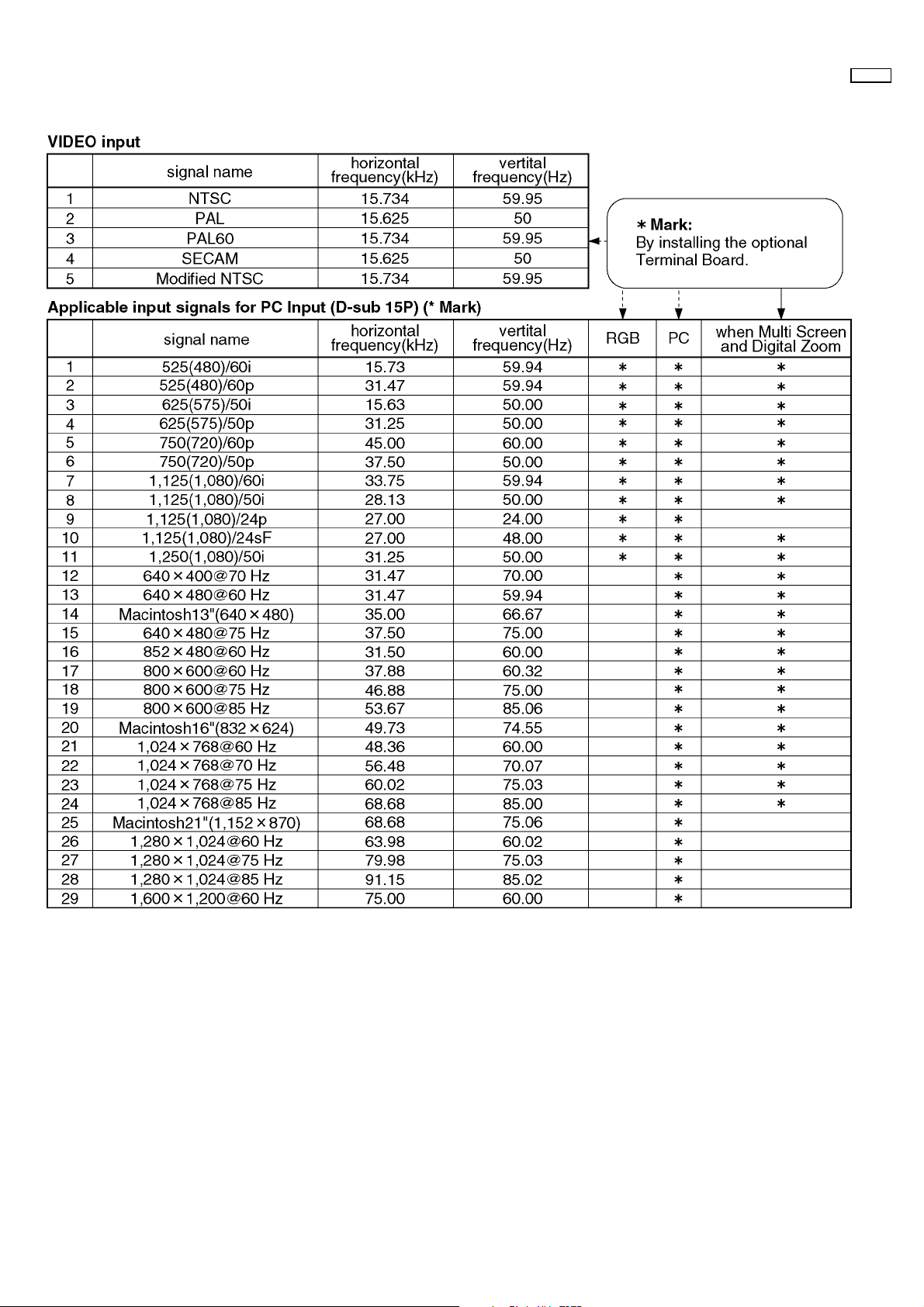
1 Applicable signals
42WP37
– 3 –
Page 4
42WP37
2 Safety Precautions
2.1. General Guidelines
1. When servicing, observe the original lead dress. If a short circuit is found, replace all parts which have been overheated or
damaged by the short circuit.
2. After servicing, see to it that all the protective devices such as insulation barriers, insulation papers shields are properly
installed.
3. After servicing, make the following leakage current checks to prevent the customer from being exposed to shock hazards.
2.1.1. Leakage Current Cold Check
1. Unplug the AC cord and connect a jumper between the two
prongs on the plug.
2. Measure the resistance value, with an ohmmeter, between
the jumpered AC plug and each exposed metallic cabinet
part on the equipment such as screwheads, connectors,
control shafts, etc. When the exposed metallic part has a
return path to the chassis, the reading should be between
1M9 and 5.2M9.
When the exposed metal does not have a return path to
the chassis, the reading must be
.
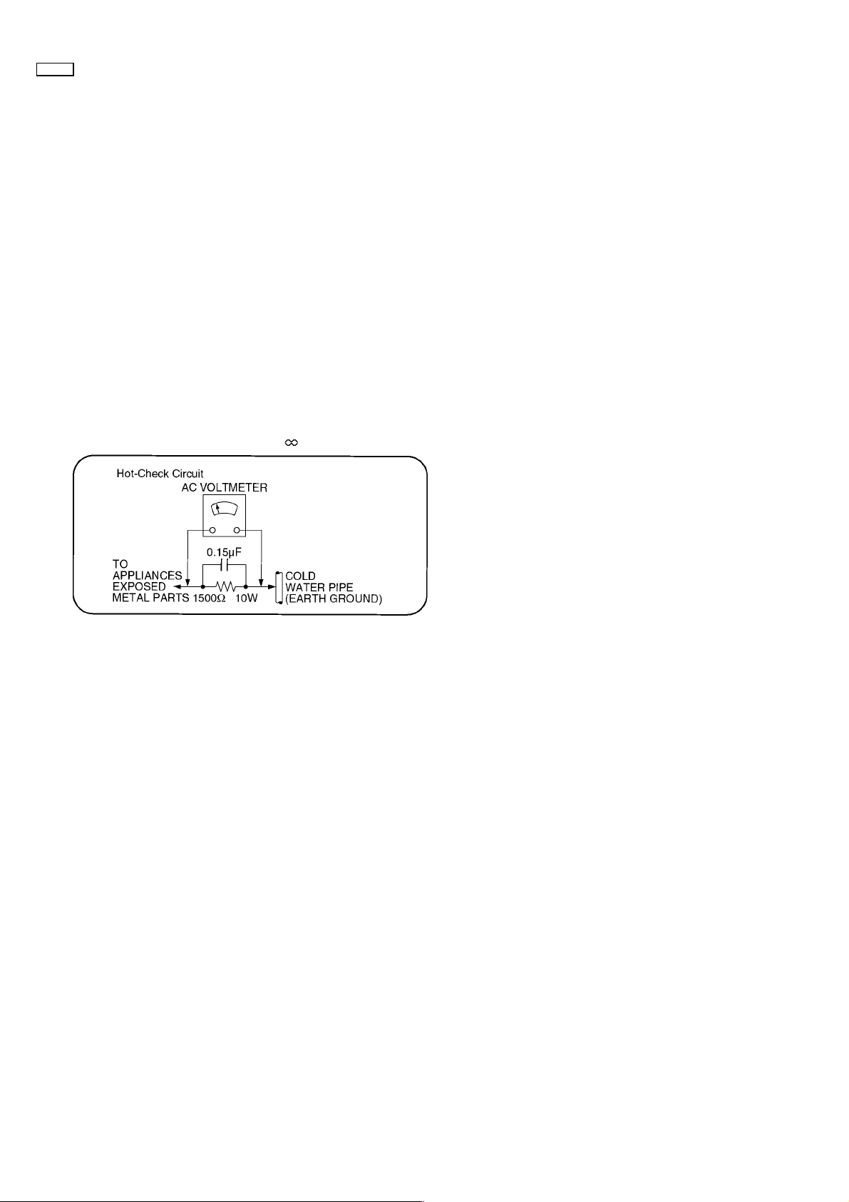
Figure 1
2.1.2. Leakage Current Hot Check (See
Figure 1.)
1. Plug the AC cord directly into the AC outlet. Do not use an
isolation transformer for this check.
2. Connect a 1.5k9, 10 watts resistor, in parallel with a 0.15µF
capacitors, between each exposed metallic part on the set
and a good earth ground such as a water pipe, as shown in
Figure 1.
3. Use an AC voltmeter, with 1000 ohms/volt or more
sensitivity, to measure the potential across the resistor.
4. Check each exposed metallic part, and measure the
voltage at each point.
5. Reverse the AC plug in the AC outlet and repeat each of the
above measurements.
6. The potential at any point should not exceed 0.75 volts
RMS. A leakage current tester (Simpson Model 229 or
equivalent) may be used to make the hot checks, leakage
current must not exceed 1/2 milliamp. In case a
measurement is outside of the limits specified, there is a
possibility of a shock hazard, and the equipment should be
repaired and rechecked before it is returned to the
customer.
– 4 –
Page 5
3 Prevention of Electro Static Discharge (ESD) to
Electrostatically Sensitive (ES) Devices
Some semiconductor (solid state) devices can be damaged easily by static electricity. Such components commonly are called
Electrostatically Sensitive (ES) Devices. Examples of typical ES devices are integrated circuits and some field-effect transistors and
semiconductor "chip" components. The following techniques should be used to help reduce the incidence of component damage
caused by electro static discharge (ESD).
1. Immediately before handling any semiconductor component or semiconductor-equipped assembly, drain off any ESD on your
body by touching a known earth ground. Alternatively, obtain and wear a commercially available discharging ESD wrist strap,
which should be removed for potential shock reasons prior to applying power to the unit under test.
2. After removing an electrical assembly equipped with ES devices, place the assembly on a conductive surface such as alminum
foil, to prevent electrostatic charge buildup or exposure of the assembly.
3. Use only a grounded-tip soldering iron to solder or unsolder ES devices.
4. Use only an anti-static solder removal device. Some solder removal devices not classified as "anti-static (ESD protected)" can
generate electrical charge sufficient to damage ES devices.
5. Do not use freon-propelled chemicals. These can generate electrical charges sufficient to damage ES devices.
6. Do not remove a replacement ES device from its protective package until immediately before you are ready to install it. (Most
replacement ES devices are packaged with leads electrically shorted together by conductive foam, alminum foil or comparable
conductive material).
7. Immediately before removing the protective material from the leads of a replacement ES device, touch the protective material
to the chassis or circuit assembly into which the device will be installed.
Caution
Be sure no power is applied to the chassis or circuit, and observe all other safety precautions.
8. Minimize bodily motions when handling unpackaged replacement ES devices. (Otherwise hamless motion such as the brushing
together of your clothes fabric or the lifting of your foot from a carpeted floor can generate static electricity (ESD) sufficient to
damage an ES device).
42WP37
– 5 –
Page 6
42WP37
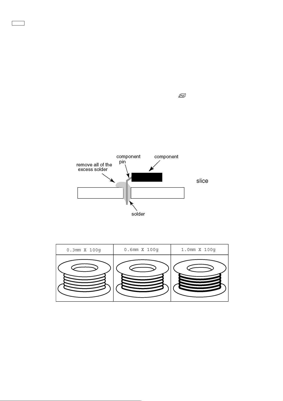
4 About lead free solder (PbF)
Note: Lead is listed as (Pb) in the periodic table of elements.
In the information below, Pb will refer to Lead solder, and PbF will refer to Lead Free Solder.
The Lead Free Solder used in our manufacturing process and discussed below is (Sn+Ag+Cu).
That is Tin (Sn), Silver (Ag) and Copper (Cu) although other types are available.
This model uses Pb Free solder in it’s manufacture due to environmental conservation issues. For service and repair work, we’d
suggest the use of Pb free solder as well, although Pb solder may be used.
PCBs manufactured using lead free solder will have the PbF within a leaf Symbol
Caution
·Pb free solder has a higher melting point than standard solder. Typically the melting point is 50 ~ 70 °F (30~40 °C) higher.
Please use a high temperature soldering iron and set it to 700 ± 20 °F (370 ± 10 °C).
·Pb free solder will tend to splash when heated too high (about 1100 °F or 600 °C).
If you must use Pb solder, please completely remove all of the Pb free solder on the pins or solder area before applying Pb
solder. If this is not practical, be sure to heat the Pb free solder until it melts, before applying Pb solder.
·After applying PbF solder to double layered boards, please check the component side for excess solder which may flow onto
the opposite side. (see figure below)
Suggested Pb free solder
There are several kinds of Pb free solder available for purchase. This product uses Sn+Ag+Cu (tin, silver, copper) solder.
However, Sn+Cu (tin, copper), Sn+Zn+Bi (tin, zinc, bismuth) solder can also be used.
stamped on the back of PCB.
– 6 –
Page 7
5 PCB Structure sheet of GP6D chassis
Board Name Function Remarks
D Digital Signal Processor 1
J Slot Interfa ce & SYNC processor 1
Z Audio out, DC-DC converter
SS Sustain Out 1
SC Scan out 1
SU Scan connection (Upper) 1
SD Scan connection (Lower) 1
C1 Data Drive (Lower Right)
C2 Data Drive (Lower Left)
H3 Speaker terminal
S1 Power switch
SS2 Sustain connection (Upper)
SS3 Sustain connection (Lower)
V1 Front SW. & Remote receiver
PF Line filter
P Power supply 1
HX PC_type_Input terminal
HZ (RTB033) RCA Component Video terminal
HV (RTB031) RCA Composite Video terminal
HT (RTB032) 21pin SCART terminal
Remarks
1. Recommend PCB´s for initial service for GP6D chassis.
42WP37
1
– 7 –
Page 8
42WP37
6 Service Hint
SS3
– 8 –
Page 9
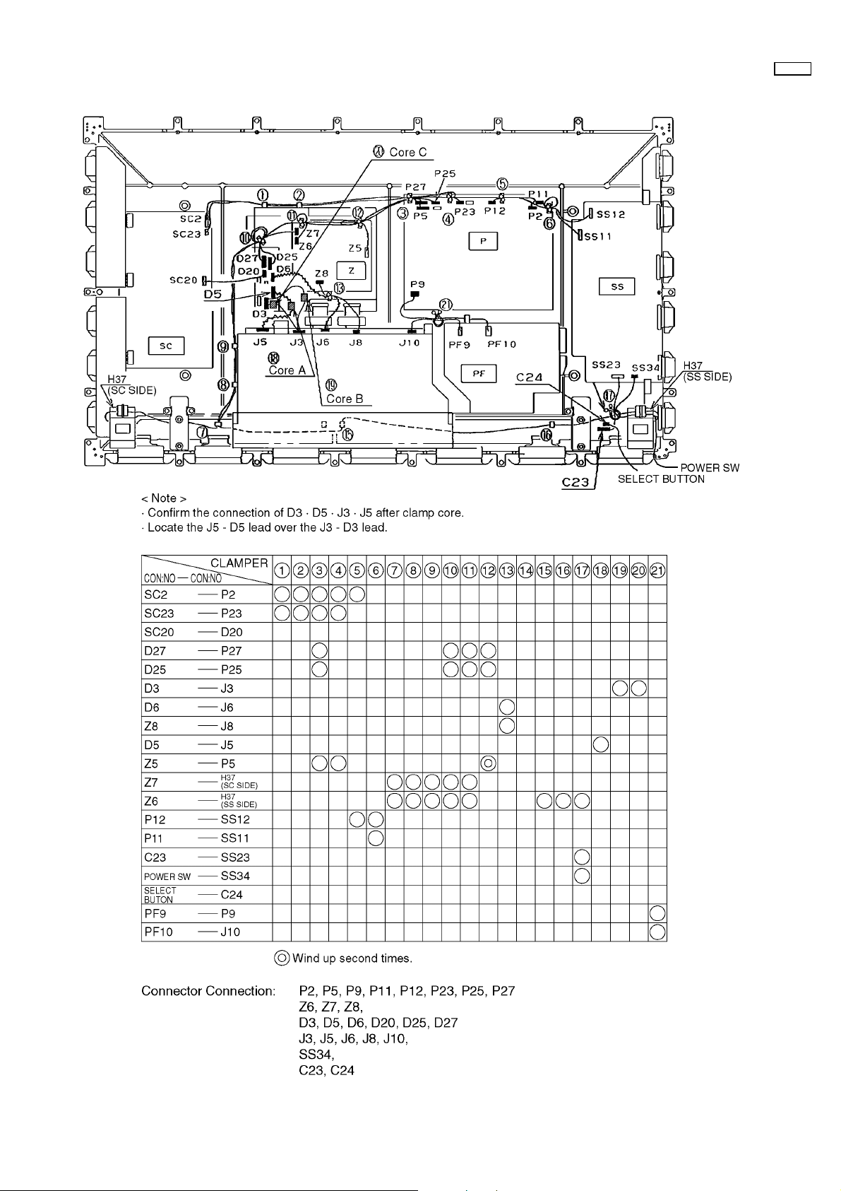
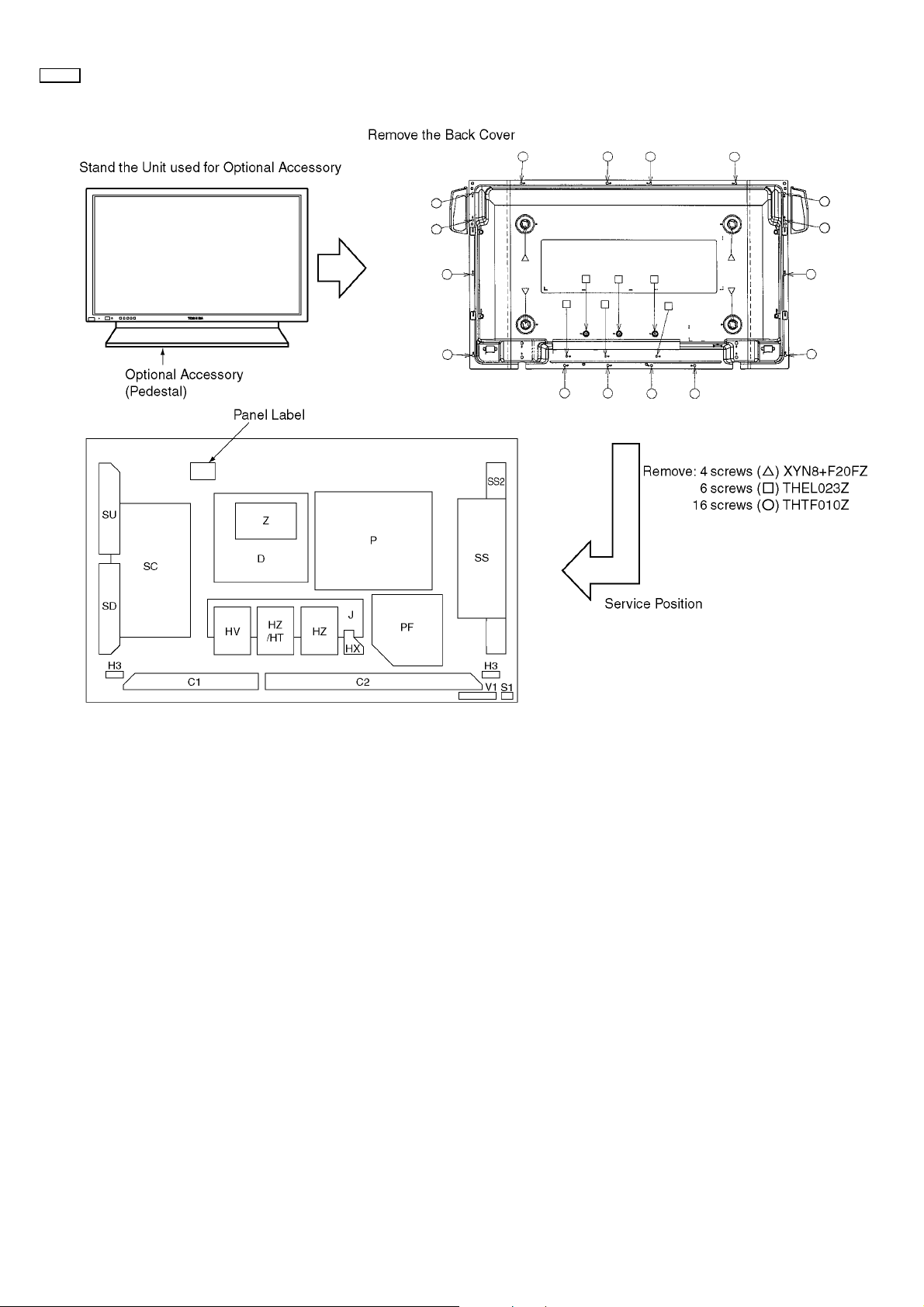
7 Location of Lead Wiring
42WP37
– 9 –
Page 10
42WP37
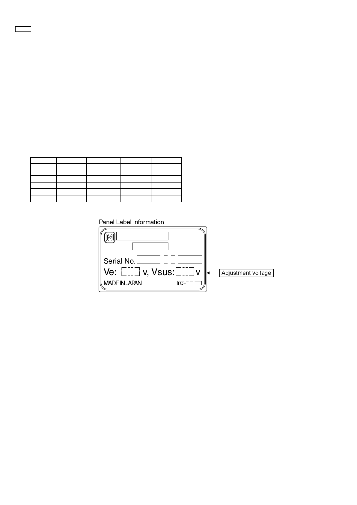
8 Adjustment Procedure
8.1. Driver Set-up
8.1.1. Item / Preparation
1. Input an APL 100 % white signal.
2. Set the picture controls: -
Picture mode: Normal
White balance: Cool
Aspect: 16:9
8.1.2. Adjustments
Adjust driver section voltages referring the panel data on the
panel data label.
Use a non conductive tool for adjustment.
Name Test Point Voltage Volume Remarks
Vsus TPVSUS
(SS)
Vbk TPVBK (SC) 155V ± 5V R6443 (SC)
Ve TPVE (SS) Ve* ± 1V R6774 (SS)
Vad TPVA (SC) -90V ± 1V R6477 (SC)
Vda TPVDA (SS) 67V ± 1V R590 (P)
Vsus* ± 1V R605 (P)
*See the Panel label
– 10 –
Page 11
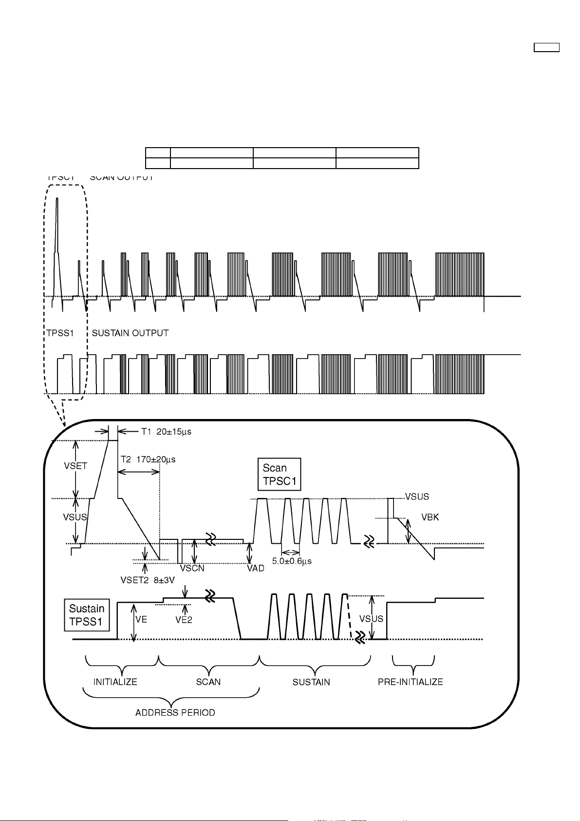
8.2. Initialization Pulse Adjust
1. Input a Cross hatch signal.
2. Set the picture controls: -
Picture mode: Normal
White balance: Cool
Adjust the indicated test point for the specified wave form.
Test point Volume Level
T2 TPSC1 (SC) R6557 (SC) 170 ± 20µ Sec
42WP37
– 11 –
Page 12
42WP37
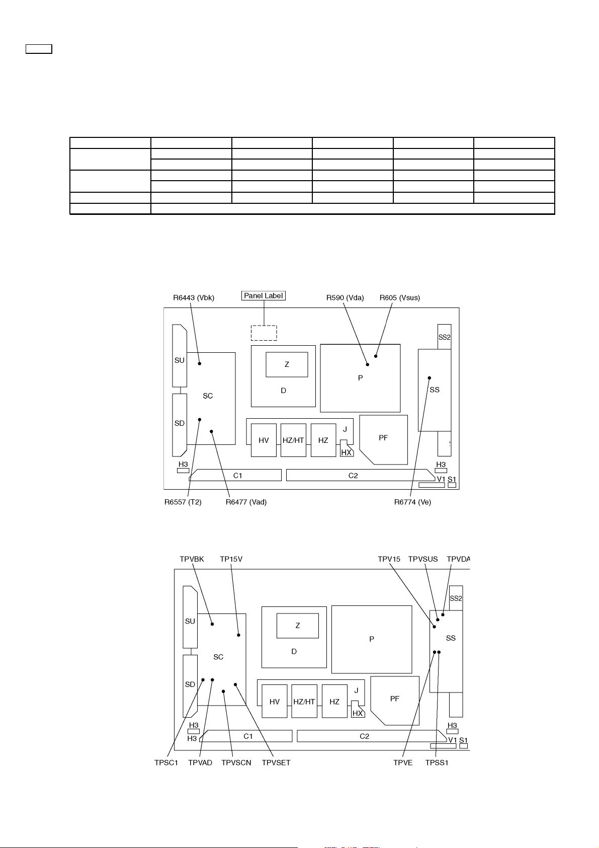
8.3. P.C.B. (Printed Circuit Board) exchange
8.3.1. Caution
1. To remove P.C.B. , wait 1 minute after power was off for discharge from electrolysis capacitors.
8.3.2. Quick adjustment after P.C.B. exchange
P.C.B. Name Test Point Voltage Volume Remarks
P Board Vsus TPVSUS (SS) Vsus* ± 1V R605 (P)
Vda TPVDA (SS) 67V ± 1V R590 (P)
SC Board Vbk TPVB K (SC) 155V ± 5V R6443 (SC)
Vad TPVAD (SC) -90V ± 1V R6477 (SC)
SS Board Ve TPVE (SS) Ve* ± 1V R6774 (SS)
D Board White blance
*See the Panel label.
8.4. Adjustment Volume Location
8.5. Test Point Location
SS3
SS3
– 12 –
Page 13
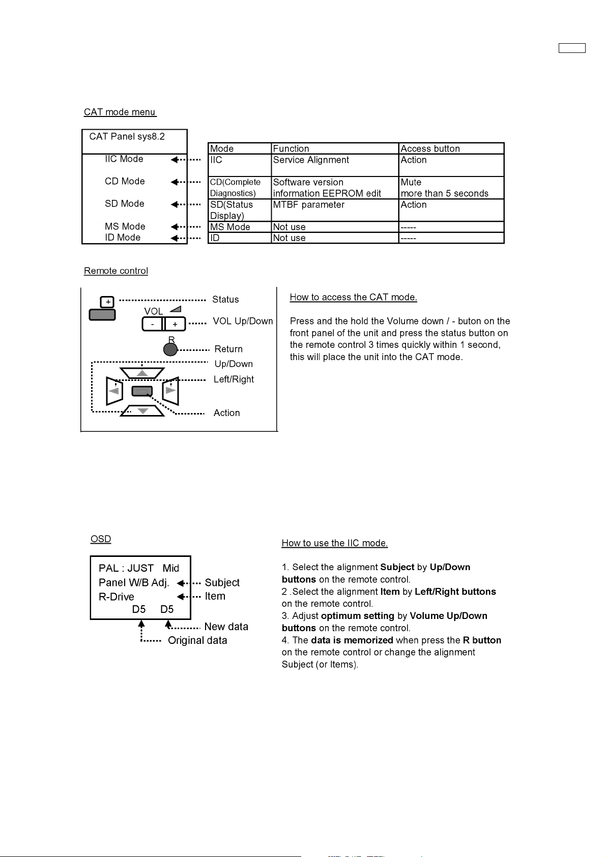
9 Service mode
9.1. CAT (computer Aided Test) mode
42WP37
To exit the CAT mode, access the ID mode and switch off the main power.
9.1.1. IIC mode
Select the IIC mode by Up/Down button on the remote control at the front page of CAT mode then press the Action button on
the remote control.
Subject and item are mentioned on page 14.
To exit the IIC mode, press the R button on the remote control.
– 13 –
Page 14
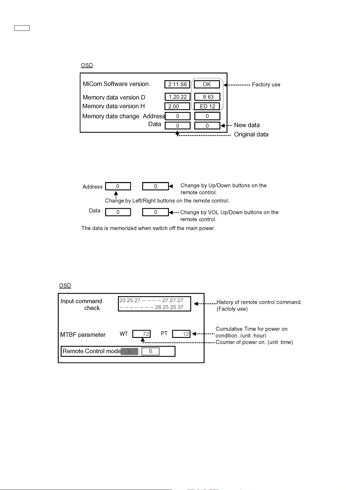
42WP37
9.1.2. CD mode
Select the CD mode by Up/Down button on the remote control at the front page of CAT mode then press the Mute button on the
remote control more than 5 sec.
Micom software version (IC9705), this version can be upgrade by
1. replace of new version IC
2. Loading the new version software from loader tool, TZSC07036.
Memory data change
To exit the CD mode, press the R button on the remote control.
9.1.3. SD mode
Select the SD mode by Up/Down button on the remote control at the front page of CAT mode then press the Action button on the
remote control.
To exit the SD mode, press the R button on the remote control.
– 14 –
Page 15
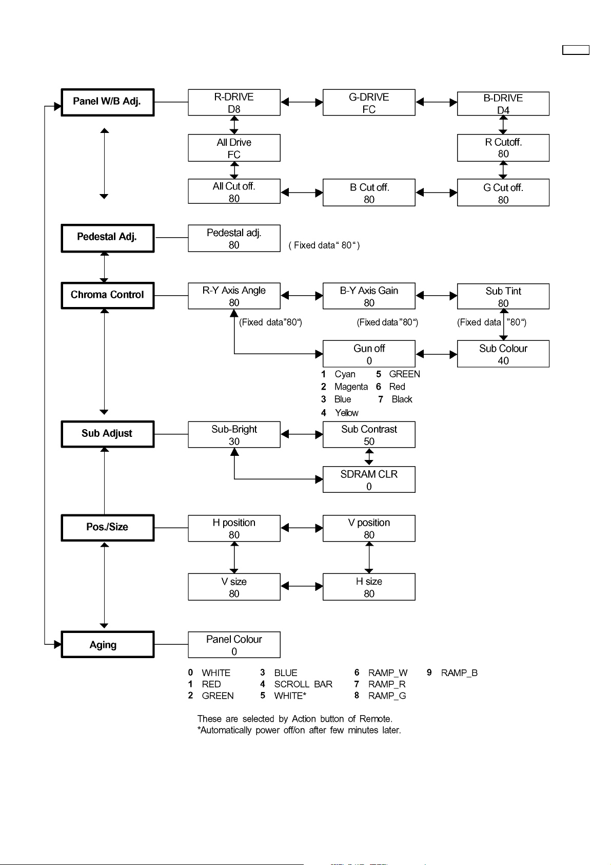
9.2. IIC mode structure (following items value is sample data.)
42WP37
– 15 –
Page 16
42WP37
10 Alignment
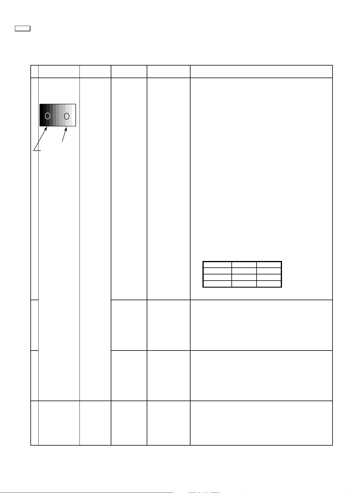
10.1. 625i/625p panel white balance
INPUT Alignment menu ProcedureEquipment Setting
1 PC (625i) Color Picture: 1) Find the nearest area to brightness of 10 cd/m2 as Low
Gray Scale Analyzer Normal Sub Adjust light by color sensor.
Pattern White balance: Sub Bright 2) Adjust Sub bright to set Low light level to 10 cd/m
Cool
Aspect: PANEL W/B
16:9 G cut off 3) Set G cut off to " 80 ".
Component /RGB-in
Component shown Fig.-02.
High light 75% Sub Adjust
Low light 15% Sub Bright 5) If Sub Bright is changed re-adjust it to set Low light
PANEL W/B
PANEL W/B
PANEL W/B
exactly.
B cut off 4) Adjust B and R cut off to set color temperature as
R cut off
2
to 10 cd/m
6)Find 75% of white area by color sensor.
G Drive 7) Set G Drive to " E8 ".
B Drive 8) Adjust B and R Drive to set color temperature
R Drive as shown Fig.-02.
.
2
9) Repeat procedure 4) to 7) to set both Low light and
high light.
PANEL W/B
All Drive 10) Set All Drive to "FC".
PANEL W/B
R,G,B cut off 11) Re-adjust Low light level again.
Color Temp. x y
Cool(Hi) 0.276 0.276
Normal(Mid) 0.288 0.296
Warm(Low) 0.313 0.329
Fig. -02
2 Picture: 1) Change white balance to "Normal".
Normal PANEL W/B
White balance: R,G,B cut off 2) Repeat procedure 3) to 11) of Cool mode.
Normal
PANEL W/B
Aspect: R,G,B Drive
16:9
3 Picture: 1) Change white balance to "Warm".
Normal PANEL W/B
White balance: R,G,B cut off 2) Repeat procedure 3) to 11) of Cool mode.
Warm
PANEL W/B
Aspect: R,G,B Drive
16:9
4 Picture: Picture Menu 1) Change color templature to "Cool".
Normal Sub Adjust
White balance: Sub Bright 2)Re-set Sub bright to "30"
Cool
Aspect:
16:9
– 16 –
Page 17
Alignment menu ProcedureEquipment Setting
5 Picture:PC (525i) 1) Write down each color temaparature of R,G,B drive and
Normal Cut off data as follows.
Aspect:
16:9
White
White balance:
Cool
Normal
Warm
Balance Cool Normal Warm
R Drive
G Drive
B Drive
R Cut off
G Cut off
B Cut off
2) Input 525i signal.
3) Copy 625i R,G,B drive and cut off data of each white
balance mode to 525i position.
42WP37
– 17 –
Page 18
42WP37
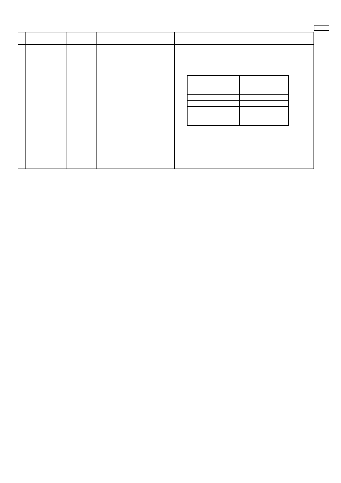
10.2. PC/RGB panel white balance
INPUT Alignment menu ProcedureEquipment Setting
1 PC (VGA) Color Picture: 1) Find the nearest area to brightness of 10 cd/m 2 as Low
Gray Scale Analyzer Normal Sub Adjust light by color sensor.
Pattern White balance: Sub Bright 2) Adjust Sub bright to set Low light level to 10 cd/m
Aspect: PANEL W/B
Component /RGB-in
High light 75% Sub Adjust
Low light 15% Sub Bright 5) If Sub Bright is changed re-adjust it to set Low light
Cool
exactly.
16:9 G cut off 3) Set G cut off to " 80 ".
PANEL W/B
B cut off 4) Adjust B and R cut off to set color temperature as
RGB shown Fig.-03.
R cut off
to 10 cd/m
2.
6)Find 75% of white area by color sensor.
PANEL W/B
G Drive 7) Set G Drive to " E8 ".
PANEL W/B
B Drive 8) Adjust B and R Drive to set color temperature
R Drive as shown Fig.-03.
9) Repeat item 4) to 7) to set both Low light and
high light.
PANEL W/B
All Drive 10) Set All Drive to "FC".
2
PANEL W/B
R,G,B cut off 11) Re-adjust Low light level again.
Color Temp. x y
Cool(Hi) 0.276 0.276
Normal(Mid) 0.288 0.296
Warm(Low) 0.313 0.329
Fig. -03
2 Picture: 1) Change white balance to "Normal".
Normal PANEL W/B
White balance: R,G,B cut off 2) Repeat procedure 3) to 11) of Cool mode.
Normal
PANEL W/B
Aspect: R,G,B Drive
16:9
3 Picture: 1) Change white balance to "Warm".
Normal PANEL W/B
White balance: R,G,B cut off 2) Repeat procedure 3) to 11) of Cool mode.
Warm
PANEL W/B
Aspect: R,G,B Drive
16:9
4 Picture: Picture Menu 1) Change color templature to "Cool".
Normal Sub Adjust
White balance: Sub Bright 2)Re-set Sub bright to "30"
Cool
Aspect:
16:9
– 18 –
Page 19
10.3. HD panel white balance
INPUT Alignment menu ProcedureEquipment Setting
1PC(HD:720i or 1080i) Color Picture: 1) Find the nearest area to brightness of 10 cd/m2 as Low
Gray Scale Analyzer Normal Sub Adjust light by color sensor.
Pattern White balance: Sub Bright 2) Adjust Sub bright to set Low light level to 10 cd/m
Cool
Aspect: PANEL W/B
16:9 G cut off 3) Set G cut off to " 80 ".
PANEL W/B
Component /RGB-in
Component shown Fig.-04.
B cut off 4) Adjust B and R cut off to set color temperature as
R cut off
High light 75% Sub Adjust
Low light 15% Sub Bright 5) If Sub Bright is changed re-adjust it to set Low light
PANEL W/B
G Drive 7) Set G Drive to " E8 ".
PANEL W/B
R Drive as shown Fig.-04.
exactly.
2
to 10 cd/m
.
6)Find 75% of white area by color sensor.
B Drive 8) Adjust B and R Drive to set color temperature
42WP37
2
9) Repeat item 4) to 7) to set both Low light and
high light.
PANEL W/B
All Drive 10) Set All Drive to "FC".
PANEL W/B
R,G,B cut off 11) Re-adjust Low light level again.
Color Temp. x y
Cool(Hi) 0.276 0.276
Normal(Mid) 0.288 0.296
Warm(Low) 0.313 0.329
Fig. -04
2 Picture: 1) Change white balance to "Normal".
Normal PANEL W/B
White balance: R,G,B cut off 2) Repeat procedure 3) to 11) of Cool mode.
Normal
PANEL W/B
Aspect: R,G,B Drive
16:9
3 Picture: 1) Change white balance to "Warm".
Normal PANEL W/B
White balance: R,G,B cut off 2) Repeat procedure 3) to 11) of Cool mode.
Warm
PANEL W/B
Aspect: R,G,B Drive
16:9
4 Picture: Picture Menu 1) Change color templature to "Cool".
Normal Sub Adjust
White balance: Sub Bright 2)Re-set Sub bright to "30"
Cool
Aspect:
16:9
– 19 –
Page 20
42WP37
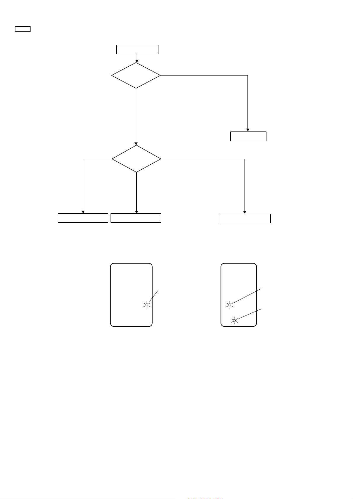
11 Trouble shooting guide
11.1. Self Check
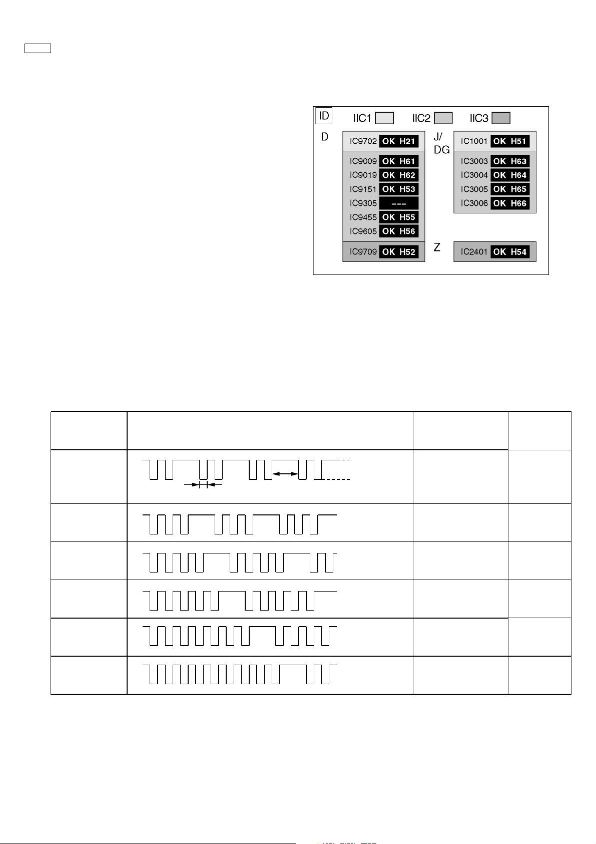
11.1.1. Display Indication
1. Self-check is used to automatically check the bus line
controlled circuit of the Plasma display.
2. To get into the Self-check mode, press the volume down
button on the customer controls at the front of the set, at the
same time pressing the OFF-TIMER button on the remote
control, and the screen will show :-
If the CCU ports have been checked and found to be incorrect
Or not located then " - - " will appear in place of " OK "
11.2. No Power (Power shut down)
11.2.1. Power LED Blinking timing chart
1. Subject
Information of LED Flashing timing chart.
2. Contents
When an abnormality has occurred the unit, the protection circuit operates and reset to the stand by mode. At this time, the
defective block can be identified by the number of blinkes of the Power LED on the front panel of the unit.
Blinking
times
2
3
4
5
Blinking timing
Once
3sec
Light
No Light
Contents
SCAN Driver1
3.3V SOS
5V SOS
Power SOS
Board
Name
SC,SU,SD
D
D,P
P
7
9
SCAN Driver2
SUS Driver
SC
SS
– 20 –
Page 21
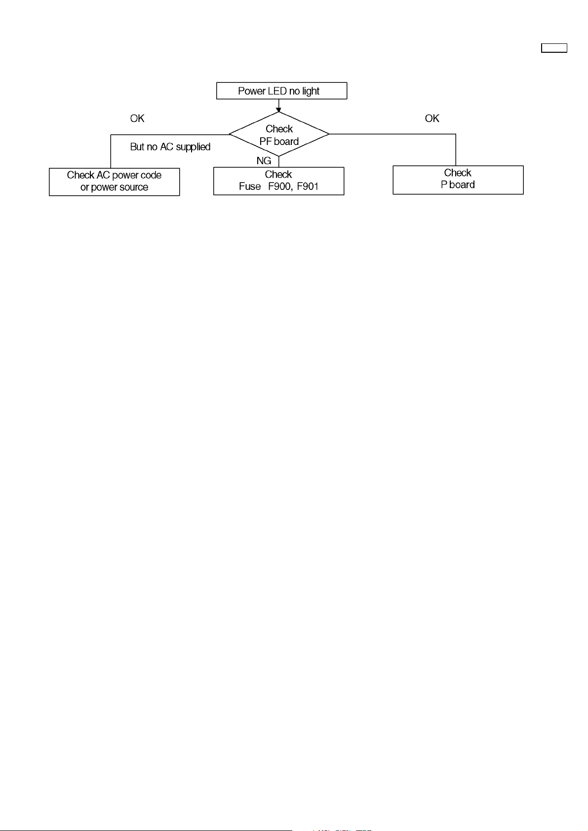
11.2.2. Power LED no light
42WP37
– 21 –
Page 22
42WP37
11.3. No Picture
No Picture
Composit/ COMPONENT/ RGB
What's signal ?
HY/ HZ / HT
board
Drive circuits LED indicator
Check
OSD
D, J
OK
all signal
board
NG
PC signal
D board
HX board
SC board SS board
D6583
D6769
(15V detection)
D6765
– 22 –
Page 23
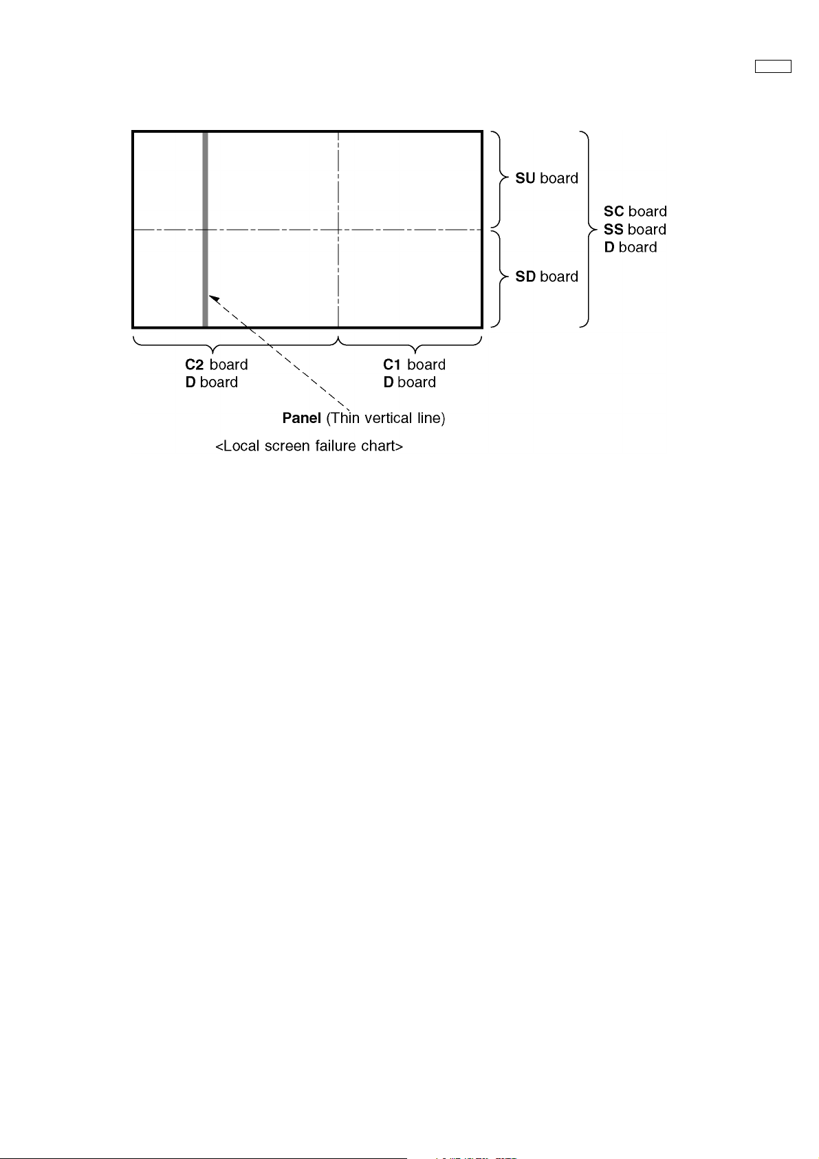
11.4. Local screen failure
Plasma display may have local area failure on the screen. Fig - 1 is the possible defect P.C.B. for each local area.
42WP37
Fig - 1
– 23 –
Page 24

42WP37
– 24 –
Page 25
12 Conductor Views
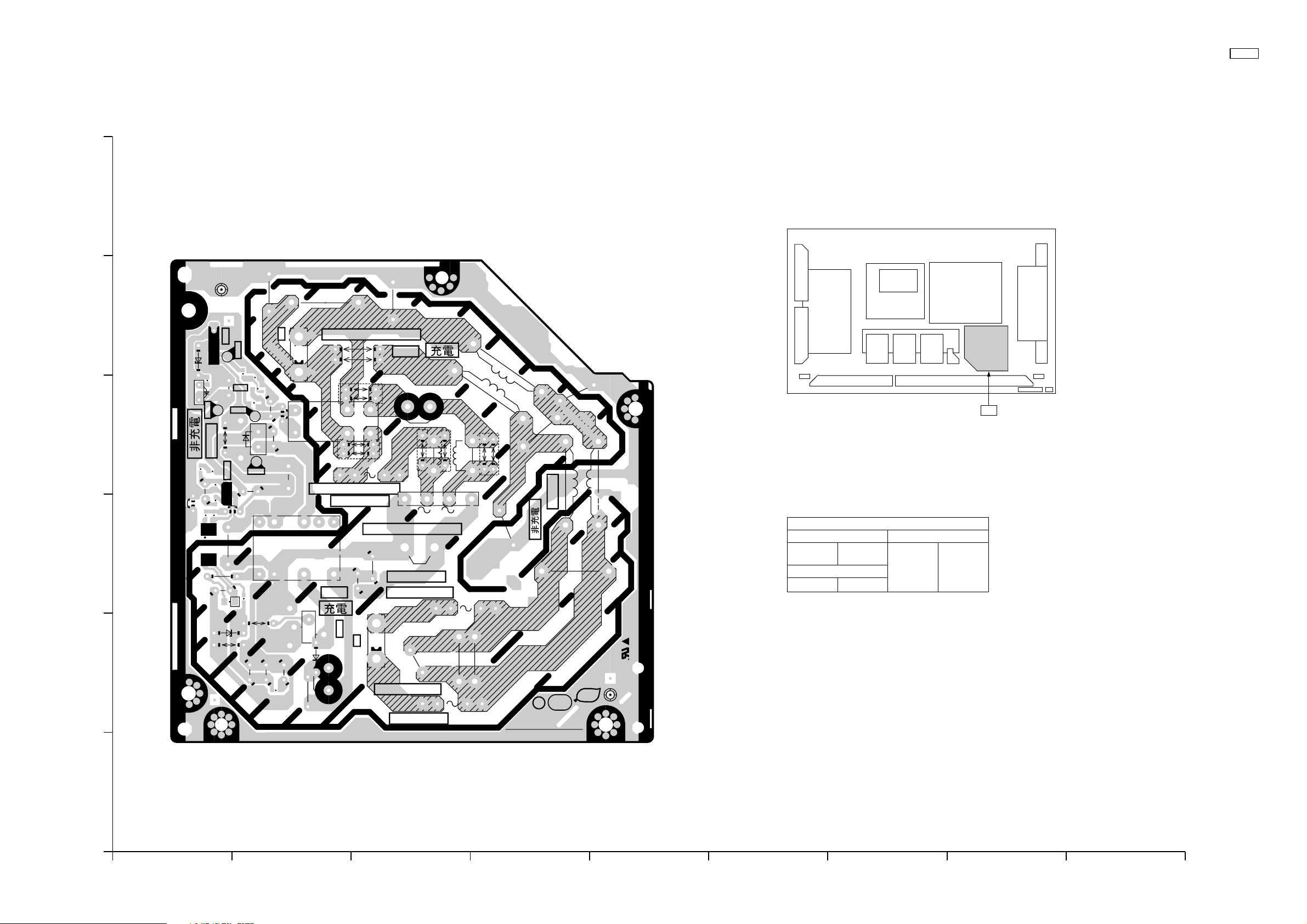
12.1. PF-Board
6
PF-BOARD
TXNPF10QBS
42WP37
C902
C912
C903
5
6
PF10
TP902
1
D921
R928
D923
TP903
4
COLD
R923
R924
R925
C924
R922
R920
D907
C923
R921
IC902
D922
TP901
A
K
Q903
R
R926
D920
C920
L904
R927
TP904
C925
C921
S1
3
V2
V1
R906
C915
D904
2
D906
C917
R907
C918
C916
R905
PF9
C922
S
RL901
T901
S2
C
D903
C914
1
LIVE CIRCUIT
4
T3.15AL250V
CAUTION
PTP2
P1
HOT
D
IC901
L906
R904
F902
C919
1
PF1
4
HOT
R903
-
D902
LIVE CIRCUIT
C913
CAUTION
T8AH250V
D901
T8AH250V
CAUTION
R902
L902
L905
+
C905
F900
R901
F901
SEE REVERSE FOR ORDER NO.
C906
1
TNPA2813
COLD
C901
PF
C904
L901
PbF
94V-0
Parts Location
IC
IC901 B-2
IC902 A-4
TRANSISTOR
Q903 B-4
PF-BOARD
TP
TP901 B-4
TP902 A-5
TP903 A-4
TP904 B-4
PF
1
PF-BOARD TXNPF10QBS PF-BOARD TXNPF10QBS
ABCDEFGH I
– 25 –
Page 26
42WP37
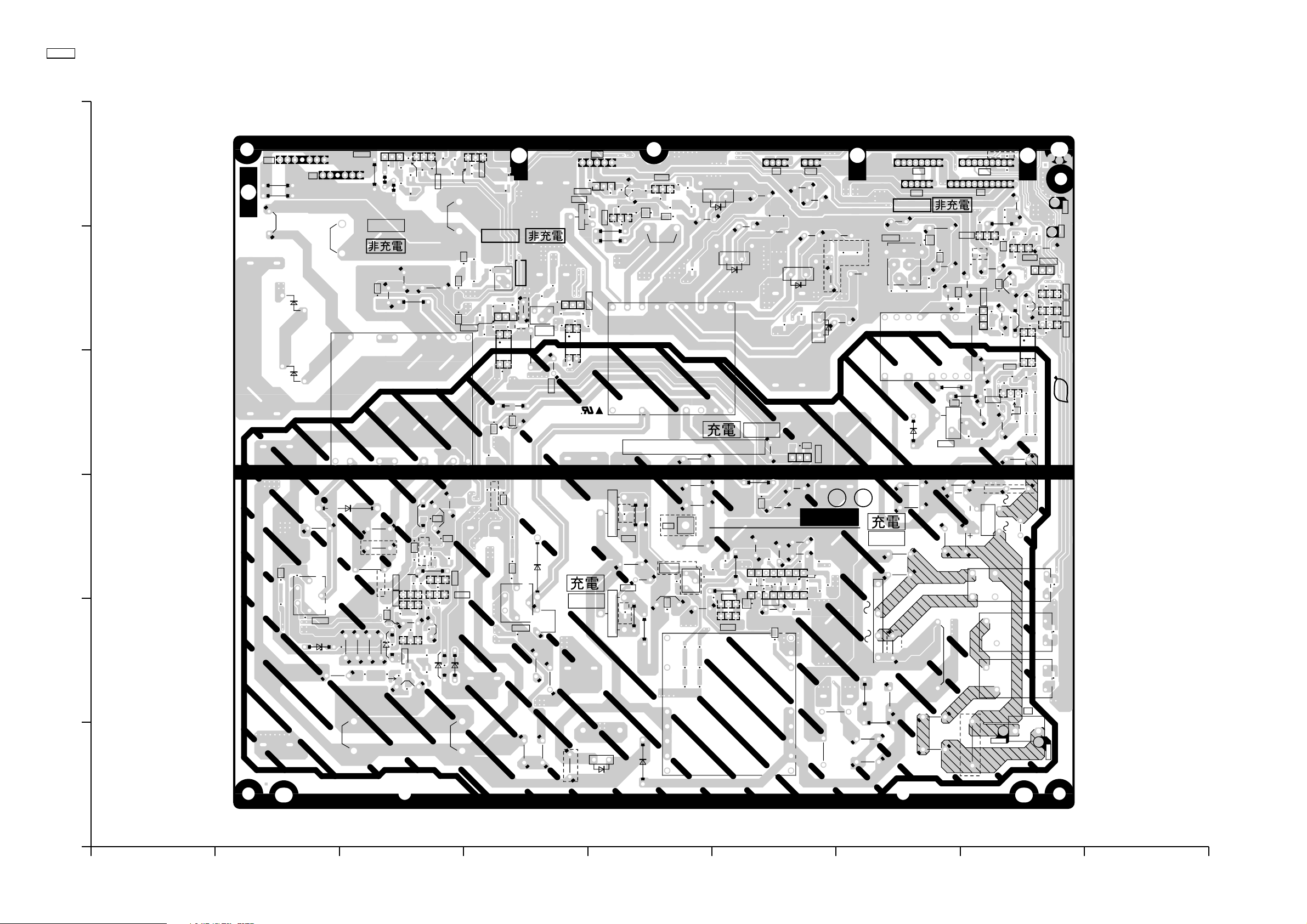
12.2. P-Board
P-BOARD(FOIL SIDE)
TNPA2841AB
6
5
P11
1
P2
R600
R597
C566
D570
D567
4
IC558
S1
R555
R598
COLD
D572
STA STB
7
16
C573
PTAP1
R552
D590
Q555
R613
R554
C569
R617
R614
D583
D584
R616
D585
R587
C574
C575
R592
S2 S4 S3
T501
P2PTB
Q557
R602
R603
D571
R584
D596
D594
COLD
R604
R605
R591
R606
R
A
R581
C561
D564
R573
C555
C568
K
L551
R585
D565
Vsus
C563
D559
R580
R561
R590
Vda
R589
R635
R588
R583
TPP1
94V-0
D595
R626
R623
R625
D592
D593
D586
IC553
V2
V1
P12
5
1
R610
KRA
IC554
Q552
G
D
S
IC557
A
K
R
C567
R582
R586
D566
C562
C578
R611
R609
D580
D578
R612
EBC
R593
Q553
R596
R599
R594
R595
R608
D579
Q554
B
C
E
R607
R601
D575
D576
C565
D574
D577
C571
D660
D661
S8S7S9S5S6S3S4S2S1
T502
P2
P1
PT
V4
V2
V3
V1
C591
14
C577
R621
P7
C590
13
P25
P10
D587
3
2
1
P1PT
8
111
5
L554
D589
C579
R618
C414
R620
S1 S2
V1
V2
V3
L401
R411
D407
P23
C422
C421
R619
C572
C564
R562
D568
D581
D582
L552
C576
D573
C570
1
1
COLD
C581
IC555
R559
5
4
C583
R615
T401
P2
D
D406
C
IC401
LIVE CIRCUIT
R563
HOT
C548
D550
IC550
2
3
1
1
R630
Q558
R631
R419
R418
D409
C416
R415
R416
KRA
V4
C411
C410
S
D405
P5
C412
P27
R628
IC402
C415
C417
Q406
C423
C407
C587
9
C586
C585
C584
R627
D410
R414
EBC
D411
R571
C409
R420
R422
C
B
Q404
R421
R417
C420
C418
C413
R428
R426
R413
R412
D408
Q405
R436
D413
R435
BC
E
R434
R407
R410
R408
R433
C403
TP50
TP51
D412
E
C419
IC403
312
R427
Q403
EBC
R424
Q402
E
C
R423
B
Q401
EBC
R425
R432
PbF
R431
R430
R429
P30
PFC
R462
R578
R572
C559
R475
R471
D454
R480
R474
R479
R473
R478
R472
R579
R650
D560
C554
D551
Q457
Q456
B
R489
R487
R488
D561
R575
R654
R493
C
B
C
R490
R491
EBC
Q455
D458
D459
R486
C558
3
D553
C551
1
2
3
R557
4
5
C550
IC551
R565
D557
2
R483
C469
R550
R560
R484
C557
R568
R577
R570
C470
R574
R502
R503
R567
D555
R485
C556
D562
D650
D651
R657
D654
R655
C
E
B
Q651
C
B
R656
E
E
Q650
E
R653
R492
C471
D460
R556
D552
D558
C468
D556
C553
R566
D
R558
D554
D563
C552
1
2
3
4
5
IC552
R564
R551
R576
R553
R569
C560
HOT
C467
D457
G
D455
R464
R463
S
Q451
C466
L452
Q454
G
R468
D456
D
R467
S
D462
R652
D652
TNPA2841
SEE REVERSE FOR ORDER NO.
R477
R476
R504
C459
R469
B
B
Q452
Q453
C
C
L451
C456
R456
D453
9
R466
R470
8
E
D463
E
R451
C452
C451
C453
C454
R409
C408
C406
C405
C455
R404
R402
C549
C650
C462
C465
C457
R465
R461
C472
C463
R494
IC451
R481
C464
D452
1
P
C461
HOT
16
R453
C460
R460
C458
R459
1
R482
+
-
D451
R452
R458
R457
R455
R454
C404
C401
RL401
C402
D404
RL403
RL402
TP008
R406
1
D401
D403
D402
P9
3
TP009
1
P-BOARD TNPA2841AB P-BOARD TNPA2841AB
ABCDEFGH I
– 26 –
Page 27
P-BOARD(COMPONENT SIDE)
TNPA2841AB
42WP37
P27
COLD
1
IC554
Q552
Vda
R590
P
HOT
D563
R576
R569
3
PMM2
L551
C563
R580
C555
IC552
1
5
C560
IC553
D565
C468
R605
ARK
2
4
G
D
S
IC557
ARK
D566
TPP1
94V-0
1
D
D
1
C581
134
COLD
P1 PT
DIP
R409
C408
C452
C451
D451
R404
D406
1
P10
IC555
52
C453
P25
C454
P12
S4
P2
ORDER
C578
5
ARK
C
Q553
E
B
R594
R595
S1
S2
PT
P1
NO.
C577
C590
D568
1
4
COLD
P7
D574
C591
D660
T502
V2
3
C548
R563
C571
S7S8
V1 V3
Q554
C565
S3
S6S5S9
V4
TNPA2841
3
L552
C421
C564
C422
1
1
IC550
2
P23
PMM4
C572
C576
C570
D573
P2
HOT
LIVE CIRCUIT
L451
R463
R467
R464
C466
G
S
R468
Q451
G
S
Q454
R652
R578
C549
C650
C462
C465
C457
IC451
16
+
1
C464
9
Q452
Q453
C456
8
R572
R469
C559
R456
PFC
P30
C459
L452
R475
R462
-
R458
R452
R451
R455
6
C419
3
5
Q403
Q402
Q401
PbF
4
3
PMM3
Q404
2
1
C420
D408
C403
C402
R406
IC403
Q406
9
11
R628
C409
R412
C585
C413
C417
C418
R
A
K
Q558
C412
D404
IC402
C410
RL401
P5
V4
S
1
C416
T401
V3 V2
IC401
C406
C404
8
1
5
L554
C579
C414
S2
S1
V1
L401
R411
D
C
C405
HOT
C455
2
RL403
RL402
Q557
Q555
IC558
K
R554
C574
C575
Vsus
T501
R592
R587
V2 V1 P2 PTB PTA P1
C556
D558
R650
Q650
D552
C471
R655
Q651
R579
R570
Q455
R577
Q457
Q456
C470
R485
R
A
6
R552
1
P11
1
R600
R597
7
R598
P2
PMM1
C573
C566
D551
C569
C557
R574
R568
D560
S1STASTBS2S4S3
IC551
R550
R560
R483
C558
3
D557
D570
D567
1
2
4
5
C469
3
1
P9
1
C401
R402
R454
R457
D462
D457
C467
R553
R551
P-BOARD TNPA2841AB P-BOARD TNPA2841AB
ABCDEFGH I
– 27 –
Page 28
42WP37
P
Parts Location
IC
IC401 G-4
IC402 H-5
IC403 H-5
IC451 F-3
IC550 F-4
IC551 B-3
IC552 D-2
IC553 D-5
IC554 E-6
IC555 G-5
IC557 D-5
IC558 C-6
P-BOARD (FOIL SIDE)
TRANSISTOR TP
Q401 H-5
Q402 H-5
Q403 H-5
Q404 H-5
Q405 H-4
Q406 H-4
Q451 E-3
Q452 F-2
Q453 F-2
Q454 E-2
Q455 C-2
Q456 C-3
Q457 C-3
Q552 D-6
Q553 E-6
Q554 E-6
Q555 C-6
Q557 D-6
Q558 H-5
Q650 C-3
Q651 C-3
TP008 H-1
TP009 H-1
TP50 H-6
TP61 H-5
TPP1 D-4
Parts Location
IC
IC401 C-4
IC402 B-5
IC403 B-5
IC451 D-3
IC550 D-4
IC551 H-3
IC552 F-3
IC553 F-5
IC554 E-6
IC555 C-5
IC557 F-5
IC558 G-6
P-BOARD (COMPONENT SIDE)
TRANSISTOR TP
Q401 B-5
Q402 B-5
Q403 B-5
Q404 B-5
Q406 B-4
Q451 E-3
Q452 D-2
Q453 D-2
Q454 E-2
Q455 G-2
Q456 G-2
Q457 G-3
Q552 F-6
Q553 E-6
Q554 E-6
Q555 G-6
Q557 G-6
Q558 B-5
Q650 G-2
Q651 G-3
TPP1 F-4
P-BOARD PARTS LOCATION P-BOARD PARTS LOCATION
– 28 –
Page 29
12.3. HX-Board
6
5
HX-BOARD(FOIL SIDE)
TZTNP02SBSE
TNPA2842
SEE REVERSE FOR ORDER NO.
PbF
4
1
6
3
2
11
JK511
CR NO.3
42WP37
HX-BOARD(COMPONENT SIDE)
TZTNP02SBSE
C564
C523
NO.
CR NO.3
D502
R787
R786
E
D506
111
HX1
D
R780
R785
C409
22
L526
C
D504
R794
Q537
R593
D505
R791
C566
C567
R790
L511
L507
L508
L509
L510
R591
R592
R526R527R528
E
R792
C565
D
R509
R508
C
1
HX
Parts Location
HX-BOARD
IC
IC3502 E-4 Q3531 D-4
TRANSISTOR
Q3532 D-4
Q3533 E-4
Q3534 E-4
Q3535 E-4
Q3536 E-4
Q3537 F-4
A
1
R586
HX
IC502
R664
ORDER
12
R400
R589
R778
8
C524
R585
5
R656
C562
B
5
D501
JK511
JK513
1
TNPA2842
PbF
HX
C551
R781
Q534
1
6
R788
R529
R784
JK509
R783
R672
R530
Q535
R782
C563
C405
C404
L555
1
Q536
R590
4
R548
L513
A
Q533
R789
B
L517
L516
D503
C550
Q531
Q532
R776 R777
R653
R511
R538
L514
R537
R655
R547
L512
R668
R663
R654
C561
JK513
5
10
15
JK509
15
6
9
5
9
D507
D508
R510
D509
D510
L515
1
HX-BOARD TZTNP02SBSE HX-BOARD TZTNP02SBSE
ABCDEFGH I
– 29 –
Page 30
42WP37
12.4. HV-Board
6
Parts Location
IC
IC3201 A-3
IC3251 B-4
HV-BOARD
TRANSISTOR
Q3002 B-2
Q3004 B-2
Q3006 B-2
Q3007 C-2
Q3051 B-2
Q3052 A-2
Q3101 B-2
Q3102 C-2
Q3104 B-2
Parts Location
IC
IC3001 G-2
IC3002 F-2
IC3003 G-2
IC3101 F-3
IC3102 G-2
IC3103 G-3
IC3104 F-2
IC3105 H-3
IC3301 H-3
IC3302 F-4
IC3303 H-3
IC3304 H-2
IC3305 H-2
IC3699 H-2
HV-BOARD
TRANSISTOR
Q3001 G-2
Q3003 F-2
Q3005 F-2
5
RTB031
HV-BOARD(FOIL SIDE)
TXNHV10QWS
1
HV
PbF
1
C202
IC201
70
R314
Q052
JK005
56
R315
R313
R051
C053
L
TNPA2844
IC251
R188
C154
C152
C149
C134
C137
R302
R304
R193
R131
JS306
R319
C055
R057
R059
JS310
GRB
28
C171
C153
C151
C150
R192
R053
R053
ORDER
29
C170
C172
R151
R125
R141
R140
R104
R117
C006
Q051
Q051
R008
R009
NO.
C251
C169
C135
R013
R017
H1
C252
R163
R165
R164
C167
C168
R156
R172
R157
R152
C136
R118
R114
C121
R130
R136
R129
R108
R102
Q104
R012
R027
R063
R006
D002
R310
R312
R311
C162
R170
R171
R169
C178
C173
R177
R134
R135
C112
C119
C115
C001
R127
R128
R132
R119
R106
Q101
Q002
Q006
R043
C017
R032
R037
R003
R004
Q004
R030
R020
JK001
CY
A1
A2
4
CR No.3
94V-0
3
C206
35
36
C212
C212
C213
C213
2
SLOT
C204
C203
C205
C208
1
C209
R307
R308
C214
C214
C211
C211
R
R
R
C210
R303
R309
C056
R055
R056
R052
R058
R054
R060
C054
JK004
12 3
HB
A39
A40
B39
B40
R120
C177
C176
C174
C175
C181
R178
C180
R180
R153
R173
R179
C140
JS305
C120
R126
C109
R133
Q102
R115
R107
R101
R042
C015
L005
R026
R007
C016
C022
JK002
R044
JS304
R047
C021
R040
L007
Q007
R046
R045
R041
R050
R039
RTB031
HV-BOARD(COMPONENT SIDE)
TXNHV10QWS
A39
A40
IC002
B39
B40
H1
C311
R301
R300
CR No.3
R159
IC104
TS302
5
C184
1
1
L105
R175
R176
R161
C165
C182
C159
C159
5
C127
Q003
R014
R014
C004
C004
C161
C144
C179
C142
C133
C160
C103
C132
C129
C105
R113
C128
C126
C125
R144
R145
64
64
R146
R142
R142
R143
R143
JS302
JS302
4
5
1
1
R036
12
R049
C007
R018
R021
R064
R031
R031
3
4
5
3
1
4
1
R025
8
5
NP
R023
R015
L003
C002
C005
R010
R011
R002
JK002
IC302
C308
L106
R185
1
IC101
R112
C020
C102
C019
C018
NP
NP
JS301
R038
L006
6
7
R028
Q023
C024
R001
TS301
R182
Q001
R174
R166
256
1
IC001
GBR
R167
R160
C163
65
65
IC003
IC003
5
5
C008
1
1
L001
R016
C330
TS303
L308
C325
R116
C187
D303
D302
D304
D301
R181
C166
C164
C164
R168
C110
C110
C113
C113
R121
R121
C111
C111
R029
R029
IC102
IC102
C114
C114
C104
C104
R122
R122
C108
C108
C023
C023
C107
C107
C014
C014
4
4
3
3
R022
R022
R019
R024
C012
C012
C
JK001
C329
C321
L307
C261
C185
C186
R183
R184
R162
C183
C117
C117
C106
C116
C106
C116
R123
R123
R065
R065
C013
C013
C011
C011
L004
C326
C009
C003
NP
R005
L002
Y
JK005
SEE REVERSE FOR ORDERNO.
TNPA2844
1
HV
HB
94V-0
Q005
R035
C122
C010
R033
R034
R048
A1A2B1 B2
C324
C320
R252
C264
R253
L251
C255
C255 C264
C256
X101
193
192
192
IC103
129
128
C123
C118
89
R139
R138
R138
R124
R124
R137
R137
D001
D001
9
C301
JS303
R061
JS309
C322
C266
L252
C263
C260
C262
C259
C157
R251
C156
C155
C147
R158
R155
C158
C138
C146
C145
C139
C143
R154
C131
IC301
4
4
C130
R189
C216
C124
1
1
14
R195
IC105
5
R194
C188
1
IC305
5
5
8
8
C316
16
C317
IC304
1
4
R062
L051
JS308
B
C051
L306
C328
C319
C265
C323
R255
R254
L104
L103
L103
C148
L102
C141
3
3
C218
C217
R208
2
2
L201
18
1
C207
R337
8
5
R338
1
4
IC699
L052
L
L
C052
325
325
C215
C254
TS100
TS101
TS102
RGR
R
C327
L305
C318
C253
C258
C257
GND
VD
HD
R305
R305
L303
L303
C313
C313
IC303
1
1
C309
R149
R148
C219
H0
PbF
JK004
1
HV-BOARD TXNHV10QWSHV-BOARD TXNHV10QWS
ABCDEFGH I
– 30 –
Page 31

12.5. HZ-Board
42WP37
6
IC
IC3001 G-3
IC3002 H-3
Parts Location
HZ-BOARD
IC
IC3002 A-3
TRANSISTOR
Q3001 G-2
Q3002 H-2
HZ-BOARD
TP
TP032 F-4
TP033 G-4
TP034 G-4
TP035 G-4
TP036 G-4
5
Parts Location
RTB033
HZ-BOARD(FOIL SIDE)
TXNHZ10RCS
TNPA2952
A1
A2
PbF
B1
CR NO.3
4
5
B2
4
1
IC002
8
ORDER
NO.
H1
3
2
JK002
R
L
R
Pr
JK001
HZ
1
A39
A40
B39
B40
B
Pb
GR
Y
RTB033
HZ-BOARD(COMPONENT SIDE)
TXNHZ10RCS
CR NO.3
JS014
R043
PbF
JS001
C016
HZ
TNPA2952
SEE REVERSE FOR ORDERNO.
JS002
R008
R009
R046
C024
1
JS003
C002
C001
A40
TP032
Y
R038
R029
R020
C009
R001
Y
A39
B39
B40
C017
C020
C019
R021
C003
NP
JS011
L001
GR B
R039
JS015
R044
R034
R010R011
C025
R002
TP034
TP033
Pr
Pb
JS016
R035
C014
16
9
8
1
IC001
R047
C013
C005
C004
NP
JS012
R003
L002
R045
R031
Pb
R040
C015
R032
R030
TP035
RL
L007
JS013
JK001
C018
R033
TP036
R041
R027 R028
NP
L003
C022
R012 R013
C026
C006
H1
R042
R024
R048
R
Pr
JS009
C023
JS004
L006
JS005
JS006
C011
C012
R025
R022
C010
Q001
R016
R018
R017
C008
R007
L004
JK002
LR
A2
B2
JS007
JS008
JS010
IC002
58
R037
D003D004
R023
R026
Q002
R014
R019
R015
C007
R006
L005
R004
A1
B1
14
C021
R036
D001
D002
H0
1
8
R005
SLOT
1 2 3
1
HZ-BOARD TXNHZ10RCSHZ-BOARD TXNHZ10RCS
ABCDEFGH I
– 31 –
Page 32

42WP37
12.6. HT-Board
Parts Location
6
IC
IC4601 B-4 Q3441 C-2
HT-BOARD
TRANSISTOR
Q3442 C-2
Q3501 B-2
Q3502 A-2
Q3503 B-2
Q3504 B-3
Q3505 A-3
Q3506 B-3
Parts Location
IC
IC3301 H-3
IC3305 G-4
IC3311 F-3
IC3441 F-2
IC3501 G-2
IC3699 F-4
IC3701 F-3
IC3702 G-3
HT-BOARD
TRANSISTOR
Q3401 G-2
Q3402 G-2
Q3461 H-2
Q3701 F-2
5
RTB032
HT-BOARD(FOIL SIDE)
TXNHT10QYS
TNPA2847
HT
ORDER
NO.
A1
4
3
JS306
94V-0
2
A2
B1
B2
H1
56
1
R413
R530
R544
R529
Q505
C512
R535
R538
TS502
R
R526
TS503
G
R532
R527
Q502
R524
R523
R548
C508
R520
R512
R515
R509
C516
R511
R508
R547
29
IC4601
28
R730
R731
JS315
JS316
R545
C303
Q506
R539
R533
R521
R518
R507
C515
Q504
C510C511
R536
R540R541 R542
TS501
R528
B
R531
R525
Q503
R522
C509
R510
R506
R549
1
R312
R534
R537
R543
Q501
C507
R519
JS307
C513
R505
R504
C517
JS312
R403
C406
1
1
1 23
2
R323
JK102
C720
JS305
C408
PbF
R311
CR NO.3
A39
A40
B39
B40
R308
R310
R309
JS313
C718
C725
C726
C727
R716
R318
JS311
C721
R448
Q441
R404
R442
R446
R443
R314
R325
R324
R316
R315
JS304
C716
C715
C714
C717
C710
R715
R712
L702
C445
R449
C321
Q442
R445
R447
R444
21
20
RTB032
HT-BOARD(COMPONENT SIDE)
TXNHT10QYS
A39A40
B39
D502
D501
IC699
PbF
JS302
C708
C703
C709
HT
TNPA2847
SEE REVERSE FOR ORDER
NO.
1
B40
D503
D504
8
C324
1
1
4
C705
R707
R727
R710
C704
L701
X701
NP
R704
R705
C322
C443
C323
5
JS314
C312
4
8
5
IC311
R327
R326
41
IC701
C706
C702
R706
R708
R709
64
R713
C707
C713
C701
R703
Q701
R452
R453
3
R450
IC441
L442
21
20
TS302
VD
R319
IC305
16
C315
1
R317
L305
C314
40
65
C711
R711
5
R717
C719
C728
C733
R714
C712
L703
NP
C410
R701
R412
R451
R702
C444
4
R408
C412
Q402
R441
C442
L441
HD
TS301
R321
R320
R313
C320
C318
9
8
R718
C724
C731
25
24
1
80
C723
C722
JS310
C409
R402
NP
C411
R410
R406
L404
R405
R407
JS308
C441
C317
R322
R720
R729
R722
R719
R305
R306
R307
C741
R723
R724
C732
IC702
C734
1
3
4
C746
L301
5
R728
C743
C744
C745
R725
C738
C309
C739
C740
C742
LC501
R721
6
C730
C729
7
R550
C514
R401
R411
R409
C402C404
Q401
L402
R551
NP NP
C504
R501
JS309
C302
C319
R4604
R414
R546
A1A2
B1
B2
H1
C4603
C4604
R4607
R4612
C4602
C4608
C4607
R4605
C4605
C4606
R4608
JS301
1
6
7
12
R516
9
16
C501
R303
2
C4609
C4610
C4611
C4612
R4557
C325
1
C326
C301
R302
C311
L302
C304
L303
C306
R502
R304
1
JK102
LC503
1
R513
8
IC501
1
R517
R514
C502 C503
C505
R461
C461
C307
6
12
7
Q461
R462
C4618
R4611
C4617
C4616
L4603
CR NO.3
L4602
L4601
C4615
C4614
C4613
IC301
5
R301
JS303
C316
LC502
NP
C506
R503
R466
R465
R463
R464
C313
L304
C305
C308
C310
94V-0
1
12
H0
1
8
HT-BOARD TXNHT10QYSHT-BOARD TXNHT10QYS
ABCDEFGH I
– 32 –
Page 33

12.7. J-Board
6
5
42WP37
J
Parts Location
J-BOARD (FOIL SIDE)
IC
IC8003 I-2
IC8004 F-2
TRANSISTOR
Q3001 G-3
Q3002 D-2
Q3003 D-2
Q3101 H-2
Q3102 H-2
Q3103 H-1
Q3104 H-2
Q3105 H-2
Q3106 H-2
Q8001 G-2
Q8002 I-2
4
J-BOARD (FOIL SIDE)
TNPA2826
R3025
C8070
C8072
JS8091
B40
B39
A40
A39
D3012
D3010
D3014
D3015
D3011
D3013
R3046
C8073
R3230
B40
B39
A40
A39
3
2
ZA3008
ZA3007
R3059
D3004
J13
B2
B1
A2
A1
ZA3005
R3145
R3146
C3002
C3003
R3005
R3006
R3007
R3008
Q3002
Q3003
R3011
R3013
R3010
R3009
R3012
R3014
C1004
C3005
C3006
R3022
R3160
R3161
JS8090
R1003
PbF
J14
12 22
C3205
111
TNPA2826 1 J
SEE REVERSE FOR ORDERNO.
123
ZA3006
R3035
R3044
R3100
R3099
R3047
R3045
R3034
R3197
R3036
R3084
R3085
R3041
J12
R3040
R3029
R3195
R3039
R3196
R3198
R3028
R8057
R8044
R8046
R8058
R8049
R8051
R8059
C8037
R8042
C8026
R8034
C8024
C8020
IC8004
R8032
R8068
R3188 R3189
R3190
R3260
R3261
R3262
R8054
R8043
R8045
R8055
R8048
R8050
R8056
C8036
R8041
C8025
R8033
R8011
R8018
J11
R8012
IC8003
C8023
C8019
R8017
R8010
R8009
R8031
B2
B1
A2
A1
R8001
R8004
ZA3001
R8002
R8003
D8003
R8025
R8026
D8001
1
20
11
C8013
R8067
R8065
R8066
R8072
C8061
R8093
10
C8060
R8081
R8077
R8079
R8029
Q8002
R8036
R8035
C8027
C8064
C8021
C8065
JS8092
C8028
ZA3002
B2
A2
1
20
11
C8014
R8070
R8082
R8078
R8080
R8069
R951
B1
D3001
A1
R8027
D8004
C8042
10
R8030
ZA3004
R8060
R8028
JS8093
C8041
C8022
D8002
R8061
R8098
R8100
Q8001
C8062
C8043
C8063
R8097
R8099
R8063R8064
R8062
R8091
C3016
C3014
R3056
R3002
R3001
R3058
R3049
R3055
ZA3003
Q3001
R3057
R3052
R3048
C3013
C3017
R3051
R3003
R3063
C3012
C3015
Q3105
Q3104
Q3101
R3130
R3132
Q3102
R3128
R3131
Q3103
C3253
R3199
R3202
R3129
R3133
B40
B39
A40
A39
C3252
C3251
R3251
R3297
C3255
R3117
C3108
R3203
R3257
R3254
R3111
C3261
C3114
R3255
JS8096
R3118
R3114
R3299
R3252
R3110
R3109
C3104
R3298
R3253
R3107
R3108
R3112
C3105
Q3106
R3102
R3105
R3101
R3104
R3204
R3201
C3106
C3113
C3260
R3200
R3113
R3256
R3103
R3106
1
J-BOARD TNPA2826 J-BOARD TNPA2826
ABCDEFGH I
– 33 –
Page 34

42WP37
J
Parts Location
J-BOARD (COMPONENT SIDE)
IC
6
5
4
J-BOARD(COMPONENT SIDE)
IC1001 F-2
IC3001 F-2
IC3002 D-2
IC3003 D-2
IC3004 D-3
IC3005 C-2
IC3006 D-2
IC3007 E-1
IC3108 B-2
IC3109 B-1
IC3201 B-2
IC3251 B-2
IC8001 A-3
IC8002 D-3
IC8003 A-2
IC8004 D-2
IC8005 A-2
IC8006 D-2
IC8007 A-1
IC8008 C-2
IC8009 C-2
IC8015 H-1
IC8016 E-2
IC8020 A-2
IC8021 D-2
IC951 F-3
IC952 F-3
TRANSISTOR
Q3010 E-3
Q3011 E-3
Q8010 E-2
Q8011 E-2
Q8012 E-2
Q8013 E-2
TP
TPJH1 A-2
TPJH2 D-2
TPJV1 A-2
TPJV2 D-2
TNPA2826
C3028
R3067
R3090
R3078
C3018
R3073
R3068
R3074
R952
R3089
L3006
R3069
C3027
R3075
R3077
C3026
R3088
R3076
R8071
5
R8094
C8051
C960
C8044
1
J3
2
L954
C954
4
1
IC8008
C8066
8
C8050
5
8
JS8099
1
4
IC8021
IC8009
R8087
C8048
R8085
R8024
C8006
R8006
NP
C8012
C8018
R8005
D8006
D8008
ZA3004
R8022
IC8002
R8007
JS8095
R8008
C8008
C8011
C8017
D3023
B2
1
B1
A2
A1
C8002
C8004
16
1
8
9
R8020
R8019
R8096
IC8004
20
1
R8040
C8034
C8067
1110
1
TPJV2
TPJH2
7
IC8006
J6
21
R3170
R3026
R3032
C8039
R8013
R8038
IC3004
L8004
C8032
L8007
C8046
R3083
IC3003
IC3002
R3033
1
R3082
1
R3027
16
89
R3030
R3031
1
16
8
16
9
8
16
1
8
9
IC3006
R3172
9
R3086
R3043
C3011
C3009
R3042
R3094
R3095
R3096
R3097
R3098
C3010
R3087
C3032
L3005
Q3011
R3037
R3038
L3003
1
45
IC3007
L8002
R8014
R8015
R8016
C8031
14
8
L8006
Q3010
R3151
C3040
Q8012
Q8013
R3214
R3150
R3219
R3215
D8011
R3231
D3003
R3153
R3152
R3140
R3141
C3041
J12
B40
B39
A40
A39
C956
R3024
Q8011
R3023
R3218
R3211
R3233
R3235
8
7
1
14
8
IC8016
L3050
C3200
D8010
R3216R3217
R3234
C8071
2
20
J8
1
19
C964
C958
L957
L958
L959
ZA3005
C963
C957
C962
R3018
89
R1001
R1002
IC3001
R3021
Q8010
R3213
R3212
R3210
R3232
R3017
C1004
R3020
R3016
C955
IC952
1
16
R3019
R3015
B2
B1
A2
A1
C968
L955
L956
L960
C961
L1001
L3002
C3008
IC1001
D1001
C967
C3004
4
1
8
5
C1003
ZA3006
C970
C969
C3007
C1002
C971
C1001
PbF
C965
C972
IC951
C966
L3001
C3001
X9350
TNPA2826
ORDER
NO.
J13
1
J
16
9
16
L952
J10
C3203
22
L951
C952
C951
J14
111
R3060
ZA3008
R3061
12
B40
B39
A40
A39
ZA3007
IC8015
C3202
1
C3201
C3204
8
32
C3020
C959
R3080
R3091
C953
C3022
C3023
L953
R3079
C3024
R3064
R3054
C3025
40
39
ZA3003
R3070
C3029
C3031
C3030
20
19
R3053
R3050
C3019
1
64
R3072
R3066
R3071
R3065
131
J5
J11
B2
B1
A2
A1
3
C8016
2
JS8098
TPJV1
R8084
C8047
R8083
ZA3002
L8001
C8001
C8033
C3266C3267
16
C8003
9
C8030
C3268
C8029
R8039
C8038
C3135
L8005
14
R8037
C8045
C3136
IC8005
8
C8040
NP
C8049
8
C3134
R8089
5
C3257
C3258
R3127
R8088
IC3251
C3111
14
15
C3110
14
15
R3123
R3124
R8090
R3120
R3122
C3116
C3112
C3117
R3115
C3254
C3256
8
21
22
C3263
C3262
R3126
R3125
C3109
8
21
22
R3121
R3116
R3142
ZA3001
C8010
D8005
D8007
IC8020
1
IC8001
8
R8095 R3081
R8021
C8005
C8007
R8023
L8003
IC8003
20
1
C8009
C8015
JS8094
D3022
11
10
1
TPJH1
7
R8052
R8047
C8035
R8053
1
4
IC8007
B40
B39
A40
A39
R3004
R3143
R3191
C3144
R3192
C3259
C3264
R3258
C3115
IC3201
C3143
C3141
C3142
R3194
R3193
JS8097
D3024
33
C3265
51
IC3109
R3093
D3021
IC3108
R3092
IC3005
52
C3021
7
1
28
R3259
C3107
7
1
28
C3118
1
J-BOARD TNPA2826 J-BOARD TNPA2826
ABCDEFGH I
– 34 –
Page 35

12.8. D-Board
D-BOARD(FOIL SIDE)
6
5
4
3
2
TZTNP01SBSE/TZTNP01SBSC
R909
CR NO.9
SEE REVERSE FOR ORDERNO.
R594
C598
R592R593
C757
R908
R903
R905
R906
R907
R917
R904
R900
R852
C755
R942
D719
R930
C450
C449
R418
R419
PbF
1
2
3
TNPA2825
C479
D1
Q597
Q596
R547
R585
42WP37
R598
R599
R919
R913
4
C760
R915
C758
5
D727
R834
R835
R853
R918
R914
R901
R898
C743
R809
R897
C754
R819
R862
R866
R416
R538
R553
D771
C767
Q716
R941
R940
R939
R449
Q715
R410
R937
R936
R935
C492
C491
C487
C490
C480
C476
C489
C475
R485
R484
C485
R487
C473
R541
R532
R509
R535
R537
1
4
1
IC708
IC710
IC707
5
8
C759
R923
R910
R829
R879
D723
R934
Q714
R933
R931
R932
C488
C481
C478
C477
C483
C482
R486
C740
5
R911
C486
L452
R489
C484
1
8
C750
R921
C748
R820
R871
D769
R839
C768
R840
D720
R451
C452
X451
C451
R452
X452
C453
C454
C455
R490
R491
R488
C470
R479
R478
R477
R482
R483
R475
C474
R870
R827
C745
4
R826
R815
3
R881
R825
R823
R824
C746
R822
R770
R830
R849
R850
R838
R372
R330
C463
1
10
R467
R885
C769
D730
C744
R841
R842
R821
C739
R828
C747
R925
C763
R362
R373
R364
R340
R339
20
IC451
11
R595
R596
C741
Q709
C756
R884
R836
R848
R352
R355
R461
R460
R322
C147
R060
C146
R107
R106
C106
R597
C599
R571
R356
C737
R572
C092
C096
R119
C088
IC016
C090
R051
R052
R053
R054
R055
R056
Q599
R586
Q598
R634
R565
R566
R567
R568
C601
R679
C602
R649
20
11
1
IC706
R577R578
10
R198
R197
C185
C193
1
4
IC156
5
8
R228
IC157
C189
C050
C112
R061
C109
C111
C107
C093
R306
R024
R113
R615
R579
C626
R629
R632
IC601
R643
R640
R653
R641
R814
R220
7
8
C198
R020
R023
11
R650
R651
R652
R945
R601
R946
R600
5
4
Q602
1
3
IC606
R624
C153
R108
R229
C203
R240
C202
R230
R243
C627
R221
C195
R166
1
R218
R217
C191
C192
14
R231
R233
C199
R018
R064
IC004
5
8
C027
IC008
1
C052
IC013
28
R050
5
C084
8
IC018
1
C108
C110
28
C056
C149
C148
R028
R019
R022
R105
R104
C048
IC007
C036
C038
C033
C040
10
11
C603
R207
1
20
10
20
1
10
11
20
1
R680
R683
Q601
R621
R618
C613
R179
R177
R206
R569
R564
R563
C164
C167
C165
C166
C170
R205
R975
R668
R667
R665
R664
60
R063
C636
R659
4
R048
1
56
R030
R126
R125
R124
29
5
C002
4
C001
1
1
56
R049
IC001
R062
C039
C034
IC006
29
R110
C030
C032
5
4
1
3
C043
R609
R994
R617
R619
R608
R604
IC604
R620
C731
R154
C187
C178
C176
C172
C168
C173
R204
C641
40
C638
41
61
R663
R660
R661
R656
R657
R831
C028
D001
C029
C120
C004
C022
4
C005
C006
L001
3
C003
C086
C087
IC012
C054
R029
C037
C051
C053
C049
R115
C076
C035
C114
C042
R114
1
C031
3
4
5
R584
R623
R655
R570
R610
R689
R611
R673
R690
R698
R678
R674
R602
R613
R614
R676
R603
R582
R583
R581
IC603
R677
R580
11
R234
C637
IC003
C011
C121
C094
1
R573
R574
10
1
IC602
20
C604
11
10
1
20
C728
R157
R784
IC703
R783
R169
R153
R167
C159
C158
R247
R246
R152
R111
R155
R151
R208
R227
R236
R202
R118
C180
C179
IC608
21
20
R669
C640
R693
1
80
R658
C015
R989
R662
C014
C018
C016
C023
4
C024
3
1
5
C012
L002
L003
C071
C070
C074
C072
C080
4
C081
3
1
5
C123
C067
R117
5
4
3
3
1
4
5
C097
R797
R622
22
R612
IC705
23
R575
C733
R576
IC704
40
1
R790
C727
R789
Q707
R806
R168
C163
R718
C162
3
4
C161
IC152
5
1
C160
D953
R959
C154
C156
C157
R180
C961
R691
R666
R692
R002
R003
C019
C017
C021
R015
C020
R013
C026
R016
10
C013
R032
11
IC023
C075
R033
C073
C079
R044
R041
C078
R046
C083
C124
L008
D003
C062
C057
L009
C061
C069
5
4
1
3
C098
C100
C101
R793
C734
R801
R802
R800
C730
C729
D729
C714
R791
R761
R725
R736
Q701
R737
R961
R962
5 1
C960
R960
+
R964
IC951
C955
L952
R952
L954
R951
L953
R723
R721
R719
R700
R716
R714
C954
R711
L951
R133
1
R134
R135
R948
C077
20
R694
IC010
C058
C059
R120
C068
C060
R730
R729
R728
L010
R727
R726
C125
IC017
C089
C091
R798
1
C706
D715
D718
1
R344
4
IC702
R764
8
5
44
C724
C726
C719
R799
21
C711
R744
R758
20
R746
C715
C716
C717
C766
R734
R735
D952
C957
R956
R957
R954
R973
D708
D712
D713
R699
R697
R696
R695
D704
R731
R587
R955
R588
R589
R958
R953
D707
D711
C735
R929
D722
R985
R928
R996
R997
R709
R724
R722
R720
R717
R590
R715
R713
R712
R710
D706
D705
R708
R707
Q703
D709
D710
IC711
R739
R738
Q704
14
C700
R949
8
5
Q719
R130
R132
R131
R805
R804
R803
D721
Parts Location
IC
IC9001 D-2
IC9003 D-3
IC9004 D-3
IC9006 D-2
IC9007 D-1
IC9008 D-3
IC9010 E-1
IC9012 D-2
IC9013 D-2
IC9016 C-2
IC9017 E-1
IC9018 D-2
IC9023 E-2
IC9152 E-4
IC9156 C-4
IC9157 C-4
IC9451 B-4
IC9601 D-5
IC9602 D-5
D
D-BOARD (FOIL SIDE)
IC9603 D-5
IC9604 D-5
IC9606 C-5
IC9608 D-3
IC9702 F-5
IC9703 D-4
IC9704 E-5
IC9705 E-6
IC9706 C-5
IC9707 B-6
IC9708 B-6
IC9710 B-6
IC9711 F-2
IC9951 E-4
TRANSISTOR
Q9596 A-1
Q9597 A-2
Q9598 C-1
Q9599 C-1
Q9601 D-5
Q9602 D-5
Q9701 E-4
Q9703 F-3
Q9704 F-2
Q9707 E-5
Q9709 C-5
Q9714 B-4
Q9715 B-5
Q9716 B-5
Q9719 F-2
1
D-BOARD TZTNP01SBSE/TZTNP01SBSC D-BOARD TZTNP01SBSE/TZTNP01SBSC
ABCDEFGH I
– 35 –
Page 36

42WP37
D-BOARD(COMPONENT SIDE)
6
5
4
3
2
TZTNP01SBSE/TZTNP01SBSC
5
4
C723
R792
1
8
R772
X703
C772
R950
C771
IC712
C774
C775
R795
D716
C705
R755
C713
C712
R756
Q710
R747
R867
R741
R748
R745
C765
R749
C707
D22
C647
C646
R591
D4
D728
40
C773
R766
41
80
81
R765
R768
R762
R754
R763
R767
Q702
R794
Q706
R771
R773
C959
C958
R750
R751
R752
R753
R757
R759
R742
1
7
9
11
1
D27
20
19
L601
2
1
12
R706
R705
R704
R703
R702
R701
C703
R732
R733
C709
40
D12
R988
R987
1
2
R774
1
D20
C951
12
1
39
1
C720
R769
C701
C718
L955
C964
D25
D3
R986
R995
C710
8
1
D10
R984
L701
R777
120
R775
R779
R782
R776
R171
R172
R743
R173
R176
C155
C962
R760
R216
R199
R226
R225
C952
R963
R998
C968
C953
C956
D954
C702
1
D6
R005
R007
R008
R009
R011
R014
C025
21
IC011
1
R035
R037
R038
R039
R042
R045
C082
C064
D5
31
C065
C063
C066
C102
C105
R796
X701
1
R170
C971
Thermal pad
C010
C122
C095
C103
C622
C618
C614
R616
C611
R109
R687
R684
R685
C722
R675
R607
R686
R688
IC701
160
R785
R787
121
C708
R778
R780
R781
23
21
19
17
15
13
12
11
10
9
7
5
R190
3
1
R966
R967
IC952
16
1
C969
C970
IC002
1
28
1
28
20
21
40
R786
C607
C609
R788
C610
D717
R682
C725
C732
R561
R112
22
20
18
16
14
8
6
4
2
A
B
9
C966
8
C967
D955
56
29
56
29
41
C606
1
C605
C608
52
53
R681
C612
R557
R242
R248
DEFGHJKLMNPRTUVW
C
C965
R965
R808
R969
R970
L956
R006
R004
R010
R012
R017
C009
R036
R034
R040
R047
R043
C113
C620
C615
208
C181IC151
86
R968
R807
1
R947
C182
R972
IC005
R001
1
28
1
C008
R031
28
1
21
20
80
IC019
61
40
41
60
C099
C623
TNPA2825
R638
157
ORDER
NO.
156
C629
IC605
C630
R991
C631
R990
R992
R993
C632
C633
1
105
104
4
R872
C151
C152
C194
X151
R301
R178
R245
R201
R187
R302
R181
R182
R192
C207
C174
C175
C169
5
R183
1
R465
R466
AAABAC
Y
Q001
R026
C047
R025
56
R129
R128
R127
29
C007
56
R057
C104
Q002
IC015
29
C055
IC009
1
80
61
60
C197
R468
44
R239
R165
C190
R164
IC155
43
C200
R027
R059
R058
C041
C046
C044
C045
R357
R376
R333
R349
15 0
CR NO.9
R122
R121
R548
R315
Q301
C634
C635
R648
R644
C301
R311
R310
R646
PbF
R645
R642
IC607
8
5
R813
R863
R812
R811
R810
C307
C309
C305
C303
5
4
C308
1
3
IC302
C302
4
L155
IC153
3
C150
C196
R219
C205
R368
C616
R605
R627
R606
R630
R633
R628
C183
C184
R200
C186
R210
R222
R223
C206
R232
R224
R203
D150
R308
R380
R353
R365
D
1
C742
R916
R944
R832
R847
C639
R846
R845
R844
D724
R639
C628
R654
X302
C312
IC303
1
8
C313
R336
R343
IC301
1
C306
C311
C304
4
5
1
R464
C460
C462
X453
R457
R458
C617
R244
C624
C625
C621
C619
R635
R625
R631
R671
R672
R670
D31
R560
R562
R558
C315
4
C461
C459
C458
R463
R637
R647
R626
R636
R459
C457
R469
R505
R450
C456
R455
IC453
R303
C316
R335
R337
8
IC452
TP0889
916
R367
C465
TP HDM
TP0887
TP VDM
C466
X702
Q708
32
33
48
49
IC709
C314
R371
R370
R366
C493
C494
C310
48
R462
C464
8
R528
R531
5
23
22
21
20
19
18
17
16
15
14
13
12
11
10
9
8
7
6
5
4
3
2
1
ABCDE
R476
C472
C471
R971
5
1
R480
25
R513
R481
D32
C764
R924
17
16
64
C752
R514
R515
R473
R474
R503
R502
R500
KLMNPRTUVWYAAAB AC
J
G
H
F
30
R472
31
50
51
R445
R447
R448
R530
R525
R526
1
1
R501
R446
R540
R920R922
C761
C762
R926
R927
R894
R896
R890
R887
R883
R895
R880
R893
R877
R889
R886
R876
R882
R874
R878
R869
R865
R833
R943
C749
C751
R816
R817
R818
R851
24
IC456
R411
R414
1
C468
C467
R875
R873
R843
R861
R868
R859
R864
R857
R860
C753
R858
R856
R837
R855
1
C469
28
R415
IC459
Q400
56
C400
R420
R413
R417
29
Parts Location
IC
IC9002 B-3
IC9005 C-3
IC9009 C-2
IC9011 B-2
IC9015 C-2
IC9019 C-2
IC9151 C-4
IC455
1
100
81
IC454
80
R506
R551
C495
L459
R559
C496
50
IC9153 D-4
IC9155 C-3
IC9301 D-4
IC9302 D-4
IC9303 D-5
IC9452 D-4
IC9453 E-2
IC9454 E-3
IC9455 E-3
IC9456 E-5
IC9459 F-5
IC9605 C-5
IC9607 D-5
IC9701 B-5
IC9709 E-5
IC9712 B-6
IC9952 B-3
D
D-BOARD (COMPONENT SIDE)
TRANSISTOR TP
Q9001 C-3
Q9002 C-2
Q9301 D-5
Q9400 F-5
Q9702 B-4
Q9706 A-4
Q9708 E-6
Q9710 A-5
TP HDM D-3
TP VDM D-3
TP0887 D-3
TP0889 D-3
1
D-BOARD TZTNP01SBSE/TZTNP01SBSC D-BOARD TZTNP01SBSE/TZTNP01SBSC
ABCDEFGH I
– 36 –
Page 37

12.9. C1-Board
6
5
42WP37
C1
C1-BOARD(FOIL SIDE)
TNPA2869
4
TNPA2869
SEE REVERSEFOR ORDER NO.
C1
1
23
1
3
2
C1-BOARD(COMPONENT SIDE)
TNPA2869
R7105
R7162
B1
A1
R7163
R7164
R7165
C7128
CB1
B40
R7114
C7153
C7103
A40
C7126
R7112
C7125
R7111
R7113
C7127
C7112
R7175
C7111
PbF
TNPA2869
ORDER
NO.
5
R7186
C7102
C7101
R7191
R7192
C7150
C7148
C7147
R7146
11
20
1
R7142
R7143
R7144
R7147
R7145
20
IC7104
C7152
10
C7151
1
R7154
R7155
R7156
R7157
R7158
R7159
C1MM1C1MM2
R7166 R7167 R7168
B1
C1
1
A1
R7169
C7130
C7129
C7156
C7157
CB2
C7113
R7116
R7115
C7114
R7176
R7117
B40
R7118
C7155
C7104
A40
C7149
20
11
IC7106
1
10
IC7103
C7145
C7146
C7143
C7116
C7161
R7136
C7159
R7120
C7158
R7119
C7144
C7160
R7121
11
R7160
R7161
IC7105
C7115
10
R7151
R7148
R7149
R7150
R7152
R7153
R7177
R7128
R7130
C7105
R7181
R7185
R7126
1
C7154
CB3
B1
A1
IC7101
R7170 R7171
R7131
R7172
C11
L7106
R7173
50
R7189
R7127
R7193
C7142
C7107
11
20
R7132
R7190
10
R7179
1
R7182
R7178
B40
A40
C1MM3
1
R7187
R7188
20
1
C12
1
C1-BOARD TNPA2869 C1-BOARD TNPA2869
ABCDEFGH I
– 37 –
Page 38

42WP37
12.10. C2-Board
6
5
C2
4
TNPA2870
12 3
TNPA2870 1
S
R
VE
E
R
EE
S
.
O
N
ER
D
OR
R
O
F
E
C2
3
2
C2-BOARD(FOIL SIDE)
C2-BOARD(COMPONENT SIDE)
TNPA2870
R7309
L7207
C21
C7201
C7202
1
20
R7228
C22
R7306
150
L7208
C7242
C7252
R7311
10
R7229
1
R7281
R7279
R7282
20
11
R7278
IC7201
R7308
R7266
R7307
R7305
R7267
R7310
R7289
B1
A1
C7253
C7206
R7226
R7230
R7227
R7232
R7290 R7291
R7292
CB4
C7238
C7251
B40
A40
R7235
R7233
R7239
R7260
R7259
R7258
R7257
IC7204
R7263
R7264
10
1
R7262
C7237
C7249
C7217
R7238
R7286
R7261
C7218
11
20
C7250
R7249
R7253
R7250
R7254
IC7203
R7251
R7255
R7252
R7256
10
1
11
20
C7246
C2MM2
R7244
R7243
R7248
11
20
IC7202
C7244
CB5 CB6
110
R7241
R7242
R7247
R7246
R7245
B1
A1
C7235
C7236
C7254
C7203
R7295 R7296 R7297
R7293 R7294
C7211
C7226
C7228
R7211C7239
R7212 R7213
C7212
C7225
C7227
C2TNPA2870 1
ORDER
NO.
R7287
PbF
B40
A40
R7214
R7298
R7299
B1
C7255
A1
C7204
C2MM1
R7300
C7232
C7230
B40
A40
R7216 R7217
R7218
R7215
Q7201
D7202
D7201
D7204
R7221
C7231
C7229
C7213
C7214
R7268
R7223
R7222
R7224
C7210
D7203
Q7202
C24
R7285
C23
11
R7219
C7207
C7240
C7219
C7220
R7240
R7269
R7236 R7237
1
8
R7270
L7209
R7205
1
C7243
CB7
B1
C7245
C7247
C7248
R7234
A1
C7256
C7406
R7303
R7301
R7304
R7302
B40
A40
1
C2-BOARD TNPA2870 C2-BOARD TNPA2870
ABCDEFGH I
– 38 –
Page 39

12.11. SC-Board
6
SC-BOARD(FOIL SIDE)
TXNSC10QBS
42WP37
SC
5
TP41 TP42
TP40
A20
A19
B20
B19
C637
TP43
TP45
TP44
SC41
A2
A1
B2
B1
TP56
TP57
TP55
TP58
R550
TP54
B
C
E
Q550
C598
A20
A19
B20
B19
SC42
A20
A2
A1
A19
B2
B20
B1
B19
SC43
R510
A2
R513
A1
B2
B1
C513
TP61
TP63
TP62
TP59
TP60
A20
A19
B20
B19
SC44
TP46
TP47
TP49
TP51
TP48
TP50
A2
A1
B2
B1
PbF
C639
TP36
TP37
L605
C646
Q671
4
3
E
B
Q673
E
B
C604
C603
C602
C601
2
EBC
C
Q672
R671
R673
R447
R448
C
C605
R601
L602
TP2
TP4
TP5
TP1
SC2
16
TNPA2867 1 SC
SEE REVERSE FOR ORDERNO.
R443
CRNo.6
Q601
GDSGDSGDSGDS
K
D621
D620
AAKAA
L620
L621
L622
L623
TP6
TP7
L604
13
SC23
TP9
C608
Q602
L615
TP8
L616
Q605 Q606
L611
D622
L645
L612
12
3
6
45
C523
K
D629
AA
L634
L635
L636
L637
TP15
K
TP26
L644
AA
TP29TP30TP31TP32TP33TP34TP35
TP23
TP39
TP11
TP20
TP27
TP28
TP10
TP52
TP22
TP21
TP38
TP18
TP17
TP16
TP14
K
D624
L624
L625
L626
L638
TP19
C656
TP12 TP13
R523
C521
AA
L627
L628
C621
C622
C623
R557
C526
C650
C624
TP24 TP25
L472
C550
C476
R477
R465
C456
Q624
C625
C626
Q621
SDGSDG
R499
R498
C627
C628
C629
C492
Q491 Q492
EBC EBC
D583
C459
C470
C461
C655
R474
C475
R454
T471
T451
C455
R616
T461
1
10
56
C469
1
SC-BOARD TXNSC10QBS SC-BOARD TXNSC10QBS
ABCDEFGH I
– 39 –
Page 40

42WP37
6
SC
SC-BOARD(COMPONENT SIDE)
TXNSC10QBS
5
A20
C512
R517
R518
D511
A19
R645
B20
B19
5
8
Q553
R478
R477
TPVSCN
R457
R458
D451
R489
R482
R587
3
R590
2
Q581
C460
D584
C585
R584
Q501
R585
IC542
4
1
Q556
R597
R598
D460
R476
C649
D465
D466
23
1
D467
D456
4
R491
R594
R492
B
C
R493
Q492
R591
E
IC581
5
8
R589
C584
D583
1
4
IC511
C511
R515
C541
D
D
R505R506 R507R508
C505
C506
C507
D505
D506
D507
C575
C576
C577
R575
R576
C476
R470
D491
D492
C492
B
Q491
C
E
R596
R497
R595
R583
D582
4
1
D586
R652
R649
R650
R651
D486
R654
D485
C580
814
14
IC501
1
7
1
D484
2
D458
34
D488
1
R467
R468
D459
D483
4
3
2
A2
A1
R653
B2
C581
IC502
B1
R665
D464
R485
D489
R666
D490
8
D509
R509
C509
C462C463
7
D487
C465
C464
R579
IC455
R496
R495
R475
Q472
Q471
R449
R450
Q452
Q455
R608
R609
Q463
Q462
6
13
D472
C469
C461
D496
4
4
4
6
6
6
13
13
13
D475
D470
R474
R484
C655
C472
D473
R473
BCE
1
Q475
C474
C453
D452
C452
C475
D455
R454
4
R455
E
B
1
Q451
C454
R453
C
C468
D518
C455
R616
D516
4
1
E
C467
B
Q461
C466
C
R615
R610
R486
IC454
IC453
C473
R572
5
D461
4
6
13
13
34
34
3
4
D453
3
4
D519
T461
D478
R487
D462
R488
Q477
C503
C504
4
D503
D463
R500
D502
D469
6
D474
4
Q474
12
12
2
D454
12
D517
10
6
R561
D477
D550
R469
IC472
Q476
R464
R471
R564
GS
R563
R503
R504
6
4
4
G
6
D504
3
1
R573
Q555
3
1
S
R574
R431
R502
R479
IC471
R480
C502
C478
T471
D476
8
R465
C456
L471
R622
5
C477
R459
1
IC451
8
L451
R456
R460
Q454
IC452
C459
C458
T451
R629
D468
IC456
5
C620
R433
D479
R617
R618
4
R621
D520
L453
D480
1
D481
D482
C470
R483
R512
D512
R511
8
5
R514
R516
R577
C490
C491
R499
R498
R582
R586
D585
Q511
D513
D514
G
R501
C501
C508
D508
D501
C578
R578
C550
TPVSET
IC491
C629
TPSC1
D
S
S
Q512
Q552
R571
C571
Q621
R642
R641
C493
C628
R510
A2
A1
R513
B2
C513
TPVAD
D546
D547
D548
Q582
R436
D647
8
8
9
9
C636
B1
D552
R567
R568
R540
D549
D544
L472
D545
R558
S
G
R560
C548
R559
R435
R434
D495
D536
G
C635
1
1
R647
R660
16
16
IC602
R659
C626
C625
D
D
C543
C544
C547
R432
D500
SDGSD
C634
D640
L647
C627
C598
SC42SC43SC44
A20
A2
A19
A1
B1
B20
B2
C590
R565
IC510
R566
Q503
C524
Q554
R555
Q624
R648
D637
R656
R680
R663
R698
R697
R669
R693
C624
C591
D551
C525
R538
R519
R556
R557
R523
R592
C526
R655
R678
R664
R695
R694
R670
R691
R581
R580
C532
1
45
D553
C540
D522
D524
D525
D526
R528
Q504
R527
Q551
D523
R524
C650
D636
R525
R521
R643
D515
Q520
R522
C521
D529
R593
IC521
IC512
C589
R588
C588
R562
Q502
K
D624
C642
A
R644
L627
L628
D635
R602
R603
R681
R686
R687
R688
R689
R675
Q603
C651
C652
R683
R684
R685
R682
R679
R676
R472
C621
C622
C623
B19
Q541
D541
R646
8
R541
D542
C531
IC541
D
Q521
GS
R520
R526
C523
D521
D530
D527
Q530
5
8
D531
R529
4
1
D528
D572
R539
K
C534
C529
A
R463
L624
R462
L625
L626
L638
R481
IC607
1
Q604
R452
R490
7
R466
11
IC606
R677
110
20
C546
R692
R657
R658
C656
Q542
S
R542
G
D
TNPA2867
D
R530
R531
G
S
Q522
R600
R604
R599
C670
C671
C673
C674
C675
C672
A
A
D629
L634
L635
L636L637
C471
C647
R640
14
20
R494
1
8
2
R690
1
S
S
Q543
Q544
R543
G
D
D
D
D
R532
G
G
S
Q524
Q523
C676
C487
C618
C677
C488
Q606
D612
G
D
R620
C485
C633
16
16
C486
R628
R627
1
1
8
8
IC601
IC605
C631
C632
1011
A
R638
R639
SC20
L644
1920
A20
A19
B20
B19
D570
S
S
S
Q546
Q545
R544
R545
G
D
D
R533
G
S
S
Q525
R546
G
G
D
1
SC
ORDER
D
R534
R535
G
G
S
Q526
R553
Q550
D543
B
R554
C
R569
E
S
Q548
Q547
R547
G
D
D
NO.
D
D
R536
G
S
Q527
S
Q528
CRNo.6
R625
G
S
9
9
Q614
R626
R624
Q611
D615
K
A
D622
R637
D
Q605
C615
D611
R619
R623
Q613
Q612
L618
C539
L645
R636
SCMM1
G
D
S
C617
C616
R614
L611
L612
S
D608
R613
L615
L616
R552
G
PbF
SC41
R551
R550
A2
A1
B2
B1
S
R548
R537
G
Q529
Q602
C660
D
Q549
R549
G
D
D641
D
R662
D642
S
Q601
G
R612
R611
R631
R630
A
D620
L620
L621
C608
Q642
D607
R632
K
SC23
G
R661
S
D
A
TP15V
L604
Q641
C644
C639
S
C695
C696
D
S
C611
R634
R633
A
D621
L622
13
R443
R444
G
C613
C614
C483
C484
R635
K
A
L623
C607
R442
R674
R445
B
Q672
C
R673
R671
C612
C662
C663
C481
C482
C661
C605
R601
L602
16
SC2
D645
L648
L605
R441
R446
IC604
D494
E
D493
R447
R605
R606
R607
A20
A19
B20
B19
D646
89
89
1
1
IC603
16
16
TPVBK
R667
R668
C
C
R448
R672
C637
C645
C646
E
Q671
B
E
Q673
B
C604
C603
C602
C601
1
SC-BOARD TXNSC10QBS SC-BOARD TXNSC10QBS
ABCDEFGH I
– 40 –
Page 41

SC
42WP37
Parts Location
TRANSISTOR
Q6491 E-3
Q6492 E-2
Q6550 B-5
Q6601 B-3
Q6602 B-3
Q6605 C-3
Q6606 C-3
Q6621 E-3
Q6624 E-3
Q6671 A-4
Q6672 A-4
Q6673 A-4
SC-BOARD (FOIL SIDE)
TP
TP1 A-2
TP10 C-2
TP11 C-2
TP12 D-2
TP13 D-2
TP14 D-2
TP15 D-2
TP16 D-2
TP17 D-2
TP18 D-2
TP19 D-2
TP2 A-2
TP20 D-2
TP21 D-2
TP22 D-2
TP23 D-2
TP24 D-2
TP25 E-2
TP26 C-2
TP27 C-2
TP28 C-2
TP29 C-2
TP30 C-2
TP31 C-2
TP32 C-2
TP33 C-2
TP34 B-2
TP35 B-2
TP36 A-4
TP37 A-4
TP38 D-2
TP39 C-2
TP4 A-2
TP40 A-5
TP41 A-5
TP42 A-5
TP43 A-5
TP44 A-5
TP45 A-5
TP46 F-5
TP47 F-5
TP48 F-5
TP49 F-5
TP5 A-2
TP50 F-5
TP51 F-5
TP52 D-2
TP54 C-5
TP55 B-5
TP56 B-5
TP57 B-5
TP58 B-5
TP59 E-5
TP6 B-2
TP60 E-5
TP61 E-5
TP62 E-5
TP63 E-5
TP7 B-2
TP8 B-2
TP9 B-2
Parts Location
IC
IC6451 B-3
IC6452 B-3
IC6453 B-4
IC6454 B-5
IC6455 A-4
IC6456 B-2
IC6471 B-4
IC6472 B-4
IC6491 C-2
IC6501 A-4
IC6502 A-4
IC6510 D-5
IC6511 C-5
IC6512 D-4
IC6521 D-4
IC6541 D-4
IC6542 B-4
IC6581 B-2
IC6601 E-3
IC6602 C-3
IC6603 G-4
IC6604 G-4
IC6605 E-3
IC6606 E-3
IC6607 D-3
SC-BOARD (COMPONENT SIDE)
TRANSISTOR TP
Q6451 A-3
Q6452 A-3
Q6454 B-3
Q6455 A-3
Q6461 A-2
Q6462 A-2
Q6463 A-2
Q6471 A-3
Q6472 A-3
Q6474 B-4
Q6475 A-3
Q6476 B-4
Q6477 B-4
Q6491 C-2
Q6492 B-2
Q6501 B-5
Q6502 D-4
Q6503 C-5
Q6504 D-4
Q6511 C-5
Q6512 C-4
Q6520 D-4
Q6521 D-4
Q6522 D-4
Q6523 D-4
Q6524 E-4
Q6525 E-4
Q6526 E-4
Q6527 E-4
Q6528 F-4
Q6529 F-4
Q6530 D-4
Q6541 D-4
Q6542 D-4
Q6543 D-4
Q6544 E-4
Q6545 E-4
Q6546 E-4
Q6547 E-4
Q6548 F-5
Q6549 F-5
Q6550 F-6
Q6551 D-4
Q6552 C-4
Q6553 B-4
Q6554 C-4
Q6555 B-4
Q6556 B-4
Q6581 B-2
Q6582 C-4
Q6601 F-3
Q6602 F-3
Q6603 D-2
Q6604 D-2
Q6605 D-2
Q6606 E-3
Q6611 E-2
Q6612 E-2
Q6613 E-3
Q6614 E-3
Q6621 C-3
Q6624 C-3
Q6641 F-5
Q6642 F-4
Q6671 G-4
Q6672 F-4
Q6673 G-4
TP15V F-2
TPSC1 C-5
TPVAD C-4
TPVBK G-4
TPVSCN B-3
TPVSET C-3
SC-BOARD PARTS LOCATION SC-BOARD PARTS LOCATION
– 41 –
Page 42

42WP37
12.12. SU and SD-Board
6
SU-BOARD
TNPA2957
A40
5
50
51
D6402
R6401
C6413
C6411
75
76 100
A1
C6431
C6419
IC6402
C6418
50
D6408
D6409
51
75
76
R6412
R6402
C6412
R6420
R6414
R6421
IC6401
25
1
R6423
D6405
B1B40
R6422
R6410R6411
C6417
D6403
Q6401
SU1 SU2 SU3
26
C6401
C6432
R6424
TPSU2
C6402
A40
26
B40
25
TNPA2957
PbF
1
100
C6414
D6401
ORDER
SU
SU41
A1
TPSU1
B1
NO.
1
50
51
75
76
R6403
C6415
26
25
IC6403
1
100
C6403
D6410
C6433
C6434
A40
50
IC6404
51
75
76
R6404
C6404
A1
SU
B1B40
26
25
SD
R6413
1
C6416
100
SU42
4
Parts Location
SU-BOARD
IC
IC6401 B-5
IC6402 C-5
IC6403 E-5
3
IC6404 F-5
SD-BOARD
TNPA2958
C6421
A1
D6411
R6409
B1B40
D6407
C6430
C6427
TPSD2
R6405
75
R6429
50
51
76
C6424
R6406
R6426
C6406
26
100
A40
SD1
50
51
26
IC6405
25
2
C6423
1
C6405
100
SD43
75
76
IC6406
A40
25
1
TNPA2958
ORDER
PbF
SD
SD2 SD3
NO.
1
SD44
R6425
A1
C6428
C6429
D6412
B1B40
TPSD1
C6425
50
51
75
76
R6407
R6427R6428
C6407
D6406
26
IC6407
25
1
100
A40
IC6408
R6408
C6408
75
76
100
C6422
1
51
50
25
A1
Parts Location
B1B40
C6426
26
IC
IC6405 B-2
IC6406 C-2
IC6407 E-2
IC6408 F-2
TRANSISTOR
TP
SD-BOARD
TP
Q6401 B-4
TPSU1 D-5
TPSU2 C-5
TPSD1 D-2
TPSD2 B-2
1
SU-BOARD TNPA2957
SD-BOARD TNPA2958
SU-BOARD TNPA2957
SD-BOARD TNPA2958
ABCDEFGH I
– 42 –
Page 43

12.13. SS, SS2 and SS3-Board
SS2-BOARD(FOIL SIDE)
TNPA2872
42WP37
6
TNPA2872
SEE REVERSE FOR ORDERNO.
7
1
SS47
6
2
11
1SS2
SS3-BOARD(FOIL SIDE)
5
TNPA2873
SS46
113
123
SS45
123
TNPA2873
SEE REVERSE FOR ORDERNO.
SS3 1
SS40
1
2
6
7
SS2
SS
SS3
Parts Location
TRANSISTOR
Q6701 G-2
Q6702 F-2
Q6705 F-2
Q6706 E-2
Q6721 C-2
Q6724 C-2
Q6751 F-1
Q6752 F-2
Q6753 F-2
SS-BOARD (FOIL SIDE)
TP
TP1 H-1
TP10 H-2
TP11 H-3
TP12 H-3
TP13 A-2
TP14 A-2
TP15 A-2
TP16 A-2
TP17 A-2
TP18 A-2
TP19 A-2
TP2 H-1
TP20 A-2
TP21 A-2
TP22 A-2
TP23 A-2
TP24 G-1
TP25 G-1
TP26 G-1
TP27 G-1
TP28 E-1
TP29 E-1
TP3 F-1
TP30 E-1
TP31 E-1
TP4 F-1
TP5 H-2
TP6 H-2
TP7 H-2
TP8 I-2
TP9 H-2
4
SS-BOARD(FOIL SIDE)
TXNSS10QBS
SS41A
L703
1
C703
K
D720D721
K
TP1
L702
TP2
17
SS11
C704
C702
TP10
SS41SS42SS43SS44
TP11
TP12
TP9
TP5TP6
TP7
13
7
SS48
26
1
C707
11
L705
SS12
15
TP8
SS24
1
L704
13
C701
R702
R777
R778
1
1
SS42A
PbF
13
13
123
1
456
GDSGDS
Q705Q706
Q752
E
L750
TP4
C
B
TP3
E
Q702
R774
L714
E
Q753
C
B
C
L712
Q751
B
TP26TP27
GDSGDS
Q701
L723
L722
AA
L713
L711
L721
L720
AA
TP24TP25
C753
1
1
SS43A
13
13
SS49
1
1
26
7
1
13
SS44A
13
3
TNPA2871 1 SS
SS34
1
3
SS32
3
1
11
TP13
SS23
1
TP14
2
C708
TP16
SDGSDG
C721
Q721
L727
L728
C748
D769
Q724
C726
C725
C737
C724
C723
C722
C756
L719
C754
TP15
TP21 TP22
TP20
TP19
TP18
TP17
D765
TP23
C729
C728
C727
SEE REVERSEFOR ORDERNO.
K
D724
AA
L726
L725
L724
L744
CRNo.6
D722
A
K
D729
K
AA
A
L737
L738
L745
TP31
L734
L735
L736
TP28TP29
C747
TP30
1
SS-BOARD TXNSS10QBS
SS2-BOARD TNPA2872
SS3-BOARD TNPA2873
SS-BOARD TXNSS10QBS
SS2-BOARD TNPA2872
SS3-BOARD TNPA2873
ABCDEFGH I
– 43 –
Page 44

42WP37
SS2-BOARD(COMPONENT SIDE)
TNPA2872
6
NO.
113
7
6
2
SS47
1
SS45
PbF
TNPA2872
ORDER
SS2
SS
SS2 1
SS3-BOARD(COMPONENT SIDE)
5
TNPA2873
1
7
SS46
SS40
TNPA2873
ORDER
NO.
PbF
SS3 1
2
6
113
HZ
SS3
Parts Location
IC
IC6701 D-2
IC6702 G-2
IC6703 F-2
IC6704 G-1
IC6705 H-2
IC6706 H-2
IC6711 D-2
SS-BOARD (COMPONENT SIDE)
TRANSISTOR TP
Q6701 C-2
Q6702 C-2
Q6705 D-2
Q6706 E-2
Q6711 C-2
Q6712 C-2
Q6713 D-2
Q6714 E-2
Q6721 G-2
Q6724 G-2
Q6725 H-2
Q6741 E-2
Q6742 E-1
Q6745 F-2
Q6746 G-2
Q6751 D-1
Q6752 D-2
Q6753 D-2
Q6756 F-1
Q6756 I-2
TPSS1 D-2
TPV15 B-1
TPVDA A-2
TPVE D-1
TPVSUS B-1
4
SS-BOARD(COMPONENT SIDE)
TXNSS10QBS
SS41A
1
C703
C740
C761
A
L723
K
K
C760
L722
D721
A
A
L721
L720
D720
A
C753
L703
Q701
GD
D707
R711
R712
L713 L714
C701
1
R761
C704
C702
TPVSUS
L702
1
R735
R733 R734
R732
R731
R730
13
SS41
7
26
1
SS48
3
11
R799
13
C707
SS24
1
2
L704
TPVDA
C755
L705
15
SS12
R702
SS11
7
TPV15
SS42
13
Q702
SGDS
R723
C712
C772
D708
R713
R714
C713
C714
C731
L718
Q711
D715
C741
L711
C711
Q712
C771
SS42A
C715
C717
D711
C718
C777
L750
D751
R725
TPSS1
R778
D750
TPVE
Q713
1
G
DS
R720
D712
Q714
Q741
D
Q705
GDS
1
R719
R726
16
R771
IC711
D762
R781
E
C
D759
B
Q752
R770
C
R766
R768
D758
R767
E
Q751
R728
R727
R777
1
R769
13 1
C732
89
R724
C773
C774
IC701
C733
R774
R775
R772
R773
R765
R776
E
C
B
R764
Q753
B
L712
C784
C747
C778
C775
C716
C776
SS43A
13
C786
Q706
A
D729
L734
L735
L736
L737
L738
S
R779
G
C785
D752
S
R780
G
D
13 1
D722
8
9
IC703
K
D757
R738
D761
R782
K
A
C791
AA
A
D724
L744
L724
L725
R739
TNPA2871
C749
16
D760
Q755
C748
1
R783
C742
R791
R827
R790
D769
D755
D770
Q742
R736
K
A
L745
R737
C744
D753
D754
R784
D768
L726
C781
L727
L717
G
D771
R785
1
R741
R742
L728
L747
Q745 Q746
D
S
G
5
D756
8
C746
C757
SS43
Q721
C734
D740
D
R786
IC704
SS44A
C735
ORDERNO.
C722
C721
R787
R788
G
Q724
1
C736
R760
16
R759
SDG
D741
89
IC702
S
4
1
D
C723
SS
R747
R748
C724
C737
13
S
C739
R755
R756
1
C725
D737
CRNo.6
C726
13
R744
R743
PbF
C727
D735
D767
D736
10
11
C728
D766
IC706
D765
C751
R820
R819
R818
1
SS44
1
26
SS49
R801
R802
R808
R809
R803
R807
7
R762
R763
1
3
SS34
3
1
SS32
C708
R701
11
C756
R824
1
Q756
8
D764
R825
R826
SS23
R823
1
C709
L719
R792
20
C729
R796
R821
R804
R805
R811
R812
R797
R798
R806
R810
R793
R794
R795
1
Q725
R789
IC705
D763
C750
4
5
C754
1
SS-BOARD TXNSS10QBS
SS2-BOARD TNPA2872
SS3-BOARD TNPA2873
SS-BOARD TXNSS10QBS
SS2-BOARD TNPA2872
SS3-BOARD TNPA2873
ABCDEFGH I
– 44 –
Page 45

12.14. Z-Board
42WP37
Z
Parts Location
Z-BOARD
IC
6
IC2301 B-3
IC2301 G-3
IC2302 C-3
IC2302 F-4
IC2304 G-2
IC2401 C-2
IC2401 F-2
IC801 B-2
IC801 G-2
IC802 B-2
IC802 G-2
IC803 H-2
IC804 A-3
IC804 H-3
5
Z-BOARD(FOIL SIDE)
TNPA2815
C2360
IC802
R807
C802
IC2301
C2350
R2321
Z30
3
C2357
R2331
C2461
IC2302
C2351
R2347
C2457
C2451
R2346
C2453
B
R2333
R2471
Q2331
C
C2353
C2438
R2470
R2468
C2363
R2467
R2354
R2348
R2452
E
C2435
C2437
C2480
C2355
32
1
R2466
28
1
C2433
C2450
C2452
R2486
C2456
R2482
R2352
R2460
R2356
R2360
R2447
R2450
R2463
R2484
C2369
C2315
R2304
R2481
R2448
R2431
R2301
C2429
Z7
R2350
R2485
R2449
C2442
C2431
C2365
C2419
1
3
1
4
Z6
D2317
R2307
R2308
C2432
C2427
R2457
Z31
3
R818
Q2330
B
C
C2362
C2352
R2353
3
2
D803
1
IC801
1
2
3
D802
Z
1
E
28
1
C2354
C2460
5
PbF
R2351
C2458
4
C2313
C2436
R2456
C2368
R2359
D2316
R2358
C2434
R2453
C2314
C2364
C2464
R805 R806
C808
C805
R2410
C2462
R2324
17
C2367
R2355
IC2401
16
R2477
R2476
R2320
94V-0
L2331
C2361
15
14
C2359
R2305
C2454
C2463
Z32
3
1
1
3
4
1
5
C817
L804
R812
R811
C818
R2357
C819
Z10
R813
4
R2365
3
152
IC804
L805
C813
D808
R2366
C2370
C814
C807
C812
C815
R808
C803
C810
3
C811
2
R809
C816
R819
R820
R803
C806
C809
Z33
C2366
L2330
15
14
C2358
R817
1
1
C2356
5
4
TNPA2815
SEE REVERSE FOR ORDERNO.
Z-BOARD(COMPONENT SIDE)
TNPA2815
Q2331
4
1
3
1
R2442
Z6
R2440
R2445
C2427
Q2408
C2484
ZMM3
Q2304
R2441
R2438
C2429
Z7
C2365
R2345
C2419
C2430
C2465
R2356
R2434
Q2303
R2332
C2426
Q2406
R2480
Q2410
19
R2309
C2441
R2473
R2464
C2369
C2423
R2472
R2461
20
ZMM1
R2360
28
R2310
R2439
1
C2355
C2437
32
R2462
C2363
DIP
1
R2487
C2450
C2440
2
C2353
C2459
R2483
Z8
1
BCE
IC2302
Q2306
R2469
C2451
C2438
94V-0
L2331
C2454
C2457
PbF
R2306
R2488
C2422
Q2301
C2359
R2319
C2367
D2302
Q2305
R2341
C2417
15
14
D2308
R2355
C2312
Q2302
C2474
17
16
R2408
C808
C805
R2325
IC2401
C2314
C2466
C2467
R2489
D810
D811
R2358
Q2330
E
C
C2362
C2364
C2368
28 15
R2359
1
R2343
C2354
L2305
C2313
JS2301
L2306
5
IC2304
IC801
134
L801
3
B
IC2301
R2370
Q2333
R2371
IC802
2
1
2
C802
TNPA2815
ORDER
Z30
Z31
C2352
L802
NO.
TRANSISTOR
D812
13
D813
1
C2366
D2301
L2330
C2358
R2372
R2369
3
5
4
1
14
Q2334
C809
Q2301 F-2
Q2302 F-3
Q2303 F-3
Q2304 E-3
Q2305 F-3
Q2306 F-3
Q2330 B-4
Q2330 G-4
Q2331 C-4
Q2331 F-4
Q2333 G-3
Q2334 G-3
Q2370 H-3
Q2406 F-2
Q2408 E-2
Q2410 F-2
Q801 H-3
Z32
R2365
R2357
C814
1
1
L805
3
Q2370
C810
D809
IC804
C2370
D804
C815
C813
C806
3
3
Z33
R2366
R2367
R2373
D807
D806
C803
Z
ZMM2
C817 C818
C819
5
2
9
L804
C812
1
R2368
R2399
Z10
1
5
R814
R815
4
R816
Q801
1
11
Z5
L803
C811
18
IC803
16
C816
R810
1
Z-BOARD TNPA2815 Z-BOARD TNPA2815
ABCDEFGH I
– 45 –
Page 46

42WP37
12.15. V1, S1 and H3-Board
6
V1-BOARD(FOIL SIDE)
TXNV110QBS
5
V1-BOARD(COMPONENT SIDE)
TXNV110QBS
H3
S1
4
S1-BOARD(FOIL SIDE)
TNPA2868
S1-BOARD(COMPONENT SIDE)
TNPA2868
H3
V1
3
H3-BOARD
TNPA3003
2
L8502
1
V1-BOARD TXNV110QBS
S1-BOARD TNPA2868
H3-BOARD TNPA3003
ABCDEFGH I
SEE REVERSE FOR ORDER
TNPA3003
C8001
H37
JK8500
C8002
1
3
NO.
H3
1
L8501
V1-BOARD TXNV110QBS
S1-BOARD TNPA2868
H3-BOARD TNPA3003
– 46 –
Page 47

Block and Schematic Diagrams
Schematic Diagram Notes
Important Safety Notice
Components identified by mark have special characteristics important for safety.
When replacing any of these components, use only manufacture's specified parts.
Notes:
1. Resistor
All resistors are cabon 1/4W resistor, unless marked as follows:
Unit of resistance is OHM [ Ω] (K=1,000, M=1,000,000).
: Nonflammable : Metal Oxide
: Solid : Metal Film
: Wire Wound : Fuse:
2. Capacitor
All capacitors are ceramic 50V capacitor, unless marked as follows:
Unit of capacitance is F, unless otherwise noted.
: Temperature Compensation : Electrolytic
: Polyester : Bipolar
M
m T
: Metalized Polyester : Dipped Tantalum
: Polypropylene : Z-Type
3. Coil
Unit of inductance is H, unless otherwise noted.
4. Test Point
: Test Point position
5. Earth Symbol
: Chassis Earth (Cold) : Line Earth (Hot)
6. Voltage Measurement
Voltage is measured by a DC voltmeter.
Conditions of the measurement are the following:
Power Source ...................................................
Receiving Signal ............................................... Colour Bar signal (RF)
All customer's controls ...................................... Maximum positions
7. Number in red circle indicates waveform nember.
(See waveform pattern table.)
8. When arrow mark ( ) is found, connection is easily found from the direction of arrow
9. Indicates the major signal flow. : Video Audio
10. This schematic diagram is the latest at the time of printing and subject to change without
notice.
NP
+
-
Z
AC220-240V, 50/60Hz
42WP37
Remarks:
1. The Power Circuit contains a circuit area which uses a separate power supply to isolate the
earth connection.
The circuit is defined by HOT and COLD indications in the schematic diagram. Take the
follwing precautions.
All circuits, except the Power Circuit, are cold.
Precautions
a. Do not touch the hot part or the hot and cold parts at the same time or you may
b. Do not short- circuit the hot and cold circuits or a fuse may blow and parts may
c. Do not connect an instrument, such as an oscilloscope, to the hot and cold
Connect the earth of instruments to the earth connection of the circuit being
d. Make sure to disconnect the power plug before removing the chassis.
2. Following diodes are interchangeable.
MA150- MA162 (Replacement part)
Schematic Diagram Notes
be shocked.
break.
circuits simultaneously or a fuse may blow.
measured.
– 47 –
Page 48

THIS PAGE IS
INTENTIONALLY LEFT
BLANK.
– 48 –
Page 49

42WP37
13 Replacement panel handling precautions and replacement procedure
Replacement panel
handling precautions and
replacement procedure
1 Replacement panel, Package specification
1
drawing and overview
Main parts to be removed(Returned and reused parts
•
External box, shock absorbing material, protective bags
• Escutcheon (For transport)
• Rear face cardboard • (Panel) protective sheet
• SEMS screw ×4 • Flat washer ×4
• T apping screw ×14
Parts used for replacement
(Parts not removed: )
Panel • Data module circuit
• C1 to C6 module
(
Integrated for static electricity protection etc.
• Fixing plate for H module (*)
• Isolation plate for SC module
)
Model
*Some portions of the following description are diffrent
from 42WP37 as this is written based on 50XP37.
For example, 42WP37 has C1 and C2 modules only,
50XP37 has 6 modules of C1 to C6.
The procedure and precautions are the same for both modeuls.
)
Replacement
panel
Isolation plate
for SC module
Fixing plate for
H module
*It isn't used when
a case of exchanged
unit is used AV slot
terminal board type
( )
50XP37 42WP37
Escutcheon
C1 module
(50XP37)
Protective
sheet
C6 module
C5 module
(50XP37)
C1 module
(42WP37)
(For transport)
C2 module
(50XP37)
C4 module
(50XP37)
C2 module
(42WP37)
Flat
washer
Data module circuit
Tapping screw
(14 points)
SEMS screw
2 Replacement set, Parts layout diagram and overview
Remove and reuse PARTS OTHER
THAN THOSE BELOW from the
replacement set "Part replacement"
Panel • Data module circuit
SU module
C1 module
(50XP37)
Z-module P-module
D-module
C2 module
(50XP37)
• C1 to C6 module
(
Integrated for static
electricity protection etc.
• Fixing plate for H module
•
Isolation plate for SC module
)
SC module
Note :Some installation parts and a
figure are different depends
SD module
on model.
:
Fans are installed only on
50XP37.
Panel handling precautions
2
C6 module
(50XP37)
C5 module
(50XP37)
C1 module
(42WP37)
Slot block
Ass'y
PF module
• The glass used in the plasma panel is thin, and its structure is extremely susceptible to impact, so be very careful during
handling not to damage the unit by dropping, tipping over, hitting or subjecting to any other impact.
• Numerous flexible printed leads with extremely soft structure are used around the panel. Be very careful during handling
not to damage these by pulling, bending or subjecting to any other excessive loads.
"The C1 to C6 module and data module circuit are connected with flexible leads (electrostatic protection)."
"Slanted insertion should not be attempted during flexible lead connection, as this will damage the circuit by creating
an electrical short."
• A protective sheet is attached to the back of the replacement panel to prevent scratching and deposition of debris. Before
assembly, be sure to completely remove the protective sheet, wipe the surface with a soft cloth, remove the stand pole
brackets (starting with the set to be replaced), and mount on the replacement panel.
• The replacement panel does not have stand pole brackets (2 points)
Remove the stand pole brackets from the set to be replaced before mounting the replacement panel.
C3 module
(50XP37)
C3 module
C4 module
(50XP37)
C2 module
(42WP37)
C3 module
Rear face
cardboard
SS2
module
SS module
SS3
module
Replacement work procedure and precautions
3
Preparation
• Screwdrivers,
pliers and other tools •
• Stand and placement mats
Cloth for wiping glass surface
Repair panel side Replacement set side
Remove the replacement panel
from the packaging box.
Reuse the removed outer box and shoc k absorbing materials
•
when returning a panel for replacement
Be careful of foreign matter such as screws on the
•
placement mat, as this will damage the panel.
Remove rear face cardboard.
Mount two stand pole sets
removed from the replacement
set.
• Place the panel in the stand.
Remove the escutcheon for
transport.
• Do not use the removed tapping screws for the
replacement set.
Mount PCBs,fan,lead wires,
metal fittings and screws, etc,
are removed from the
replacement set.
•
Beware of slanted insertion or floating connection
during lead insertion.
•
Completely peel off the protective sheet on the back
of the replacement panel, and wipe off any debris
and fingerprints etc.
•
Do not remove isolation plate for SC module from
replacement panel.
Do not remove fixing plate for H module from
•
replacement panel. (except a case of exchanged unit
is used AV slot terminal board type)
Mount the back cover and the
escutcheon removed from the
replacement set.
Connection of each cord and
cable [Preparation for turning on]
Request to the person in charge of service
After all replacement work has been completed and before turning on the power supply, please check that all
flexible leads and connectors have been correctly inserted, that there are no remaining required parts, and
that no unnecessary parts have been fitted.
After replacement work, some electrical adjustments may be required. See the service manual for details.
.
Using placement mat
Part replacement
Using stand
Using stand
Part replacement
Using stand
Using stand
Remove the back cover and the
escutcheon.
Remove the two stand pole
brackets.
Escutcheon mounting/removal
Hand the left and
right claws of
the escutcheon
with the hook
shaped parts.
Remove PCBs, fan,lead wires,
metal fittings and screws etc.
Mount the escutcheon for
transport and rear face card-board
on the replaced panel.
• Be careful not to tr ap fingers betw een the escutcheon
and panel.
Package the replaced panel with the
remaining packaging box materials.
Using stand
Using placement mat
Escutcheon
Using placement mat
Using placement mat
– 49 –
Page 50

THIS PAGE IS
INTENTIONALLY LEFT
BLANK.
– 50 –
Page 51

14 Parts Location
A110
A121
A122
42WP37
A123
A124
A125
A114
A113
E100
A115
A105
A112
A114
A115
A111
A109
A169
– 51 –
A109
Page 52

THIS PAGE IS
INTENTIONALLY LEFT
BLANK.
– 52 –
Page 53

42WP37
A705
A712
A713
A717
A711
A701
A705
Y104
A703
Y106
Y107
Y114
Y118
Y116
Y108
Y109
Y110
Y111
Y101
Y102
A715
A718
A716
A714
A702
A702
– 53 –
Page 54

THIS PAGE IS
INTENTIONALLY LEFT
BLANK.
– 54 –
Page 55

15 Chassis and Cabinet Replacement Parts List
WARNING: BEFORE SERVICING THIS CHASSIS, READ THE "X-RAY RADIATION PRECAUTION", "SAFETY PRE-
CAUTION" AND "PRODUCT SAFETY NOTICE" ON PAGE 3 OF THIS MANUAL.
CAUTION: The international hazard symbols " " in the schematic diagram and the parts list designate components
which have special characteristics important for safety and should be replaced only with types identical to those in the
original circuit or specified in the parts list. The mounting position of replacements is to be identical with originals.
Before replacing any of these components, read carefully the PRODUCT SAFETY NOTICE. Do not degrade the safety
of the receiver through improper servicing.
NOTICE:
··
·
The part number must be used when ordering parts, in order to assist in processing, be sure to include the
··
Model number and Description.
··
·
The PC board assembly with * mark is no longer available after the end of the production.
··
··
·
Location No. of Ixxxx (IC: integrated circuit) in the SEMICONDUCTORS
··
section indicates Icxxxx on the Schematic Diagrams. (E.g. I1001 is equalized to IC1001.)
Model : 42WP37C/42WP37E/42WP37F/42WP37H
Capacitors ............. CD : Ceramic Disk PF : Plastic Film EL : Electrolytic
Resistors ............... CF : Carbon Film CC : Carbon Composition MF : Metal Film
OMF : Oxide Metal Film VR : Variable Resistor FR : Fusible Resistor
(All CD and PF capacitors are
±5%, 50V and all resistors, ±5%, 1/6W unless otherwise noted.)
Location Parts No. Descriptiopn
No.
#1 : [42WP37C]
#2 : [42WP37E]
#3 : [42WP37F]
#4 : [42WP37H]
CAPACITORS
C403 72792010 CERAMIC DISC, 4700PF,Z
C404 72792010 CERAMIC DISC, 4700PF,Z
C405 72792010 CERAMIC DISC, 4700PF,Z
C451 72792010 CERAMIC DISC, 4700PF,Z
C452 72792010 CERAMIC DISC, 4700PF,Z
C453 72792010 CERAMIC DISC, 4700PF,Z
C466 72792007 CERAMIC DISC, 100PF,K,2KV
C468 72792015 ELECTORLYTIC, 330UF,450V
C469 72792015 ELECTORLYTIC, 330UF,450V
C548 72790092 ELECTORLYTIC, 100UF, 25V
C556 72790093 ELECTORLYTIC, 22UF, 50V
C560 72792009 CERAMIC DISC, 220PF,K,2KV
C563 72792011 CERAMIC DISC, 1000PF,Z
C564 72792004 CERAMIC DISC, 100PF,K,1KV
C566 72792008 CERAMIC DISC, 1000PF,K,2KV
C570 72792006 CERAMIC DISC, 470PF,K,1KV
C901 72792012 PLASTIC FILM, 1UF,250V
C902 72792003 CERAMIC DISC, 220PF,M
C903 72792003 CERAMIC DISC, 220PF,M
C904 72792003 CERAMIC DISC, 220PF,M
C905 72792003 CERAMIC DISC, 220PF,M
C906 72792014 PLASTIC FILM, 0.22UF,250V
C912 72792013 PLASTIC FILM, 1UF,250V
C920 72792003 CERAMIC DISC, 220PF,M
C921 72792005 CERAMIC DISC, 220PF,K,1KV
C6427 72792029 ELECTORLYTIC, 1000UF,25V
C6524 72792002 CERAMIC DISC, 1000PF,J,200V
C6525 72792002 CERAMIC DISC, 1000PF,J,200V
C6543 72792002 CERAMIC DISC, 1000PF,J,200V
C6544 72792002 CERAMIC DISC, 1000PF,J,200V
C6547 72792002 CERAMIC DISC, 1000PF,J,200V
C6639 72792031 ELECTORLYTIC, 150UF,200V
C6646 72792030 ELECTORLYTIC, 120UF,35V
C9958 72792032 ELECTORLYTIC, 2.2UF 25V
C9959 72792032 ELECTORLYTIC, 2.2UF 25V
Location Parts No. Descriptiopn
No.
RESISTORS
R406 72792019 FUSIBLE, 15OHM, 5WJ
R590 72792025 CONTROL, 10KOHMB 0.3W
R605 72792028 CONTROL, 50KOHMB 0.3W
R901 72792018 SOLID, 1MOHM,K,1/2W
R902 72792018 SOLID, 1MOHM,K,1/2W
R6443 72792026 CONTROL, 20KOHMB 0.3W
R6477 72792027 CONTROL, 5KOHMB 0.3W
COILS & TRANSFORMERS
L451 72792035 TRANSFORMER-SW, G4D4A0000048
L452 72000434 BEAD CHOKE, EXCELDR35C
L901 72792033 COIL, CHOKE, G0B123K00001
L902 72792033 COIL, CHOKE, G0B123K00001
L905 72792017 FILTER, LINE, ELF17N011A
L951 72000837 COIL, NOISE FILTER, ELKE103FA
L952 72000837 COIL, NOISE FILTER, ELKE103FA
L953 72000837 COIL, NOISE FILTER, ELKE103FA
L954 72000837 COIL, NOISE FILTER, ELKE103FA
L955 72000837 COIL, NOISE FILTER, ELKE103FA
L956 72000837 COIL, NOISE FILTER, ELKE103FA
L957 72000837 COIL, NOISE FILTER, ELKE103FA
L958 72000837 COIL, NOISE FILTER, ELKE103FA
L959 72000837 COIL, NOISE FILTER, ELKE103FA
L960 72000837 COIL, NOISE FILTER, ELKE103FA
L3001 72792041 FILTER, LC, J0HABB000003
L3006 72792040 FILTER, LC, J0E8004B0008
L3510 72000437 FILTER, EMI, TLK212T256AL
L3511 72000437 FILTER, EMI, TLK212T256AL
L3512 72000437 FILTER, EMI, TLK212T256AL
L3513 72000437 FILTER, EMI, TLK212T256AL
L3514 72000437 FILTER, EMI, TLK212T256AL
L3515 72000437 FILTER, EMI, TLK212T256AL
L3516 72000437 FILTER, EMI, TLK212T256AL
L3517 72000437 FILTER, EMI, TLK212T256AL
L6611 72792016 COIL, CHOKE, ELC16BR82L
L6612 72792016 COIL, CHOKE, ELC16BR82L
L6615 72792016 COIL, CHOKE, ELC16BR82L
L6616 72792016 COIL, CHOKE, ELC16BR82L
L6711 72792016 COIL, CHOKE, ELC16BR82L
L6712 72792016 COIL, CHOKE, ELC16BR82L
L6713 72792016 COIL, CHOKE, ELC16BR82L
L6714 72792016 COIL, CHOKE, ELC16BR82L
– 55 –
Page 56

Location Parts No. Descriptiopn
No.
T401 72792021 TRANSFORMER-SW, ETS25AD1H6AG
T501 72792024 TRANSFORMER-SW, ETS49BP116AD
T502 72792023 TRANSFORMER-SW, ETS42BV116AD
T901 72792022 TRANSFORMER-SW, ETS28AZ1E6AD
T6451 72792034 TRANSFORMER-SW, G4D1A0000072
T6461 72792020 TRANSFORMER-SW, ETS13TB139AP
SEMICONDUCTORS
I1001 72000942 IC, RS5C372A-E2 C1DB00000274
I1550 72790965 IC, B3L000000020
I2301 72792052 IC, LA4901
I2302 72792052 IC, LA4901
I2401 72000939 IC, BH3865S, LINEAR
I3001 72000387 IC, MC14052BF, GATE ARRAY
I3002 72790983 IC, C0JBBR000002
I3003 72000389 IC, CXA1315M, LINEAR
I3004 72790999 IC, CXA1875AM, LINEAR
I3005 72000941 IC, MM1519XQ C1AB00001139
I3007 72000783 IC, SN74AHC2G66HDCR
I3101 72792063 IC, PQ07VZ012ZP
I3102 72790973 IC, C0DBZLB00001
I3103 72790990 IC, C1AB00001826
I3104 72000415 IC, PST9128NR, LOGIC
I3105 72790980 IC, C0JBAZ001834
I3108 72000421 IC, AN78L05M, LINEAR
I3109 72000421 IC, AN78L05M, LINEAR
I3201 72790989 IC, C1AB00001720
I3251 72790987 IC, C0ZBZ0000684
I3301 72000411 IC, MM1065ZMR, LINEAR
I3303 72790946 IC, AN80L25RMS
I3304 72790984 IC, C0JBBZ000285
I3305 72000420 IC, JLC1562BF, 50HP81
I3502 72792113 IC, TVRN080
I3699 72792078 IC, S-24C16AFJ
I6401 72790975 IC, C0HBC0000005
I6402 72790975 IC, C0HBC0000005
I6403 72790975 IC, C0HBC0000005
I6404 72790975 IC, C0HBC0000005
I6405 72790975 IC, C0HBC0000005
I6406 72790975 IC, C0HBC0000005
I6407 72790975 IC, C0HBC0000005
I6408 72790975 IC, C0HBC0000005
I6451 72790944 IC, AN1431M, LINEAR
I6452 72790945 IC, AN78L15M, LINEAR
I6453 72790945 IC, AN78L15M, LINEAR
I6501 72000414 IC, TC74HC14AF
I6502 72000414 IC, TC74HC14AF
I6511 72790988 IC, C0ZBZ0000735
I6581 72792062 IC, NJM2903M
I6601 72790985 IC, C0ZBZ0000138
I6602 72790985 IC, C0ZBZ0000138
I6603 72790985 IC, C0ZBZ0000138
I6605 72790978 IC, C0JBAZ000005
I6606 72790978 IC, C0JBAZ000005
I6607 72792070 IC, TC74HC08AF
I7101 72790979 IC, C0JBAZ001604
I8003 72792055 IC, M52346SP, LINEAR
I8004 72792055 IC, M52346SP, LINEAR
I8015 72790417 IC, C0ZBZ0000205
I8016 72790981 IC, C0JBAZ001934
I9001 72790966 IC, C0CBCBD00008
I9002 72790986 IC, C0ZBZ0000551
I9003 72790976 IC, C0JBAB000550
I9005 72790982 IC, C0JBAZ001992
I9009 72790974 IC, C0FBAD000069
I9023 72790943 IC, 74LVC244APWL
I9151 72792060 IC, MN845041-A
I9155 72790994 IC, C3ABPJ000017
I9157 72792074 IC, TLC2933IPWL
I9301 72790992 IC, C1ZBZ0002358
I9303 72790991 IC, C1ZBZ0002357
I9454 72790995 IC, C3ABPJ000043
I9455 72792061 IC, MN84510-A
I9456 72792111 IC, TVRJ952-2
I9601 72792069 IC, TC74ACT244F
I9605 72790993 IC, C1ZBZ0002377
Location Parts No. Descriptiopn
No.
I9701 72792059 IC, MN102L230
I9702 #1 72792304 IC, TVRN072
#2 72792112 IC, TVRN071
#3 72792112 IC, TVRN071
#4 72792112 IC, TVRN071
I9704 72792039 IC, HM538123BJ8Z
I9705 72792110 IC, TVRJ951-1
I9707 72790977 IC, C0JBAE000239
I9709 #1 72792109 IC, TVRJ950-3
#2 72792312 IC, C2BBGF000491
#3 72792109 IC, TVRJ950-3
#4 72792109 IC, TVRJ950-3
I9710 72000613 IC, M51957BFP, LINEAR
I9951 72790972 IC, C0DBAMH00006
I9952 72790970 IC, C0DBAFH00021
IC401 72792057 IC, MIP2E1DMY1TV
IC402 72790420 IC, AN1431T, LINEAR
IC403 72790418 IC, AN7705F,LINEAR
IC451 72790969 IC, C0DABZG00001
IC550 72792125 IC, UPC24M18AHF, LINEAR
IC551 72790998 IC, C5HABZZ00115
IC552 72790997 IC, C5HABZZ00080
IC555 72790967 IC, C0DAAHG00007
IC801 72790968 IC, C0DAAHG00008
IC803 72790971 IC, C0DBALH00002
IC901 72792058 IC, MIP2E4DMY1TV
IC951 72000924 IC, PQ12SZ1T, 50HP81
IC952 72000382 IC, PQ09SZ1T
Q401 72000460 TRANSISTOR, 2SC3311A
Q402 72000460 TRANSISTOR, 2SC3311A
Q403 72000460 TRANSISTOR, 2SC3311A
Q404 72000460 TRANSISTOR, 2SC3311A
Q405 72790959 TRANSISTOR, B1CBGD000001
Q451 72790961 TRANSISTOR, B1DEGR000021
Q452 72000461 TRANSISTOR, 2SD2177R
Q453 72000779 TRANSISTOR, 2SB1434R
Q457 72000462 TRANSISTOR, 2SA1309A
Q552 72790960 TRANSISTOR, B1DEGQ000019, FET
Q553 72000463 TRANSISTOR, 2SB621A
Q903 72790935 TRANSISTOR, 2SD1328
Q1540 72000452 TRANSISTOR, 2SD601A
Q2330 72790934 TRANSISTOR, 2SD1266A
Q2331 72790934 TRANSISTOR, 2SD1266A
Q2370 72000453 TRANSISTOR, 2SB709A
Q3102 72790932 TRANSISTOR, 2SD1030
Q6401 23314737 TRANSISTOR, CHIP FET VDSS50 SMT 2SK620
Q6451 72790958 TRANSISTOR, B1BBCJ000003
Q6452 72792176 TRANSISTOR, 2SB0709A
Q6454 72790937 TRANSISTOR, 2SD814A
Q6462 72792176 TRANSISTOR, 2SB0709A
Q6472 72792176 TRANSISTOR, 2SB0709A
Q6491 72000465 TRANSISTOR, 2SC1473A
Q6492 72000465 TRANSISTOR, 2SC1473A
Q6511 72790963 TRANSISTOR, B1DFGL000005
Q6512 72790963 TRANSISTOR, B1DFGL000005
Q6521 72790962 TRANSISTOR, B1DFES000001
Q6522 72790938 TRANSISTOR, 2SK2993, FET
Q6523 72790938 TRANSISTOR, 2SK2993, FET
Q6524 72790938 TRANSISTOR, 2SK2993, FET
Q6525 72790938 TRANSISTOR, 2SK2993, FET
Q6526 72790938 TRANSISTOR, 2SK2993, FET
Q6527 72790938 TRANSISTOR, 2SK2993, FET
Q6530 72790928 TRANSISTOR, 2SB1073001TV
Q6542 72790942 TRANSISTOR, 2SK373100L
Q6543 72790942 TRANSISTOR, 2SK373100L
Q6544 72790942 TRANSISTOR, 2SK373100L
Q6545 72790942 TRANSISTOR, 2SK373100L
Q6546 72790942 TRANSISTOR, 2SK373100L
Q6547 72790942 TRANSISTOR, 2SK373100L
Q6554 72790936 TRANSISTOR, 2SD2185
Q6601 72790941 TRANSISTOR, 2SK3652000SB
Q6602 72790941 TRANSISTOR, 2SK3652000SB
Q6621 72790940 TRANSISTOR, 2SK3637000VE
Q6641 72790964 TRANSISTOR, B1DFHM000002
Q6642 72790964 TRANSISTOR, B1DFHM000002
Q6671 72790930 TRANSISTOR, 2SB940A
– 56 –
Page 57

Location Parts No. Descriptiopn
No.
Q6673 72790933 TRANSISTOR, 2SD1263A
Q6745 72790939 TRANSISTOR, 2SK326800L, FET
Q6746 72790939 TRANSISTOR, 2SK326800L, FET
Q6752 72790931 TRANSISTOR, 2SC1473
Q6753 72790931 TRANSISTOR, 2SC1473
Q9702 72790929 TRANSISTOR, 2SB1440
D401 72000327 DIODE, MA152K
D402 72000327 DIODE, MA152K
D403 72000327 DIODE, MA152K
D404 72792064 DIODE, S1WBA80Z
D406 72000343 DIODE, ERA22-10
D407 72790955 DIODE, B0HCMM000001
D408 72000346 PHOTO COUPLER, PC123FY2
D451 72790950 DIODE, B0FBBR000019
D457 72790952 DIODE, B0HARR000016
D462 72790949 DIODE, B0EAKT000012
D463 72000325 DIODE, M1FS4
D551 72000787 DIODE, B0BA02700021
D552 72000787 DIODE, B0BA02700021
D557 72000361 DIODE, TMPG10G3
D558 72000361 DIODE, TMPG10G3
D560 72000344 DIODE, RC3B2LFU1
D565 72000346 PHOTO COUPLER, PC123FY2
D566 72000346 PHOTO COUPLER, PC123FY2
D567 72790951 DIODE, B0HARR000009
D568 72790956 DIODE, B0HFRJ000012
D804 72000789 DIODE, B0JCPD000010
D806 72790948 DIODE, B0BC6R8A0010
D807 72790948 DIODE, B0BC6R8A0010
D901 72000340 VARISTOR, ERZV10V621P2
D902 72792001 DIODE, D4SB80Z
D903 72000379 DIODE, EG01C
D904 72792054 DIODE, M1FL20UF4063
D907 72000346 PHOTO COUPLER, PC123FY2
D921 72790947 DIODE, B0BA02000024
D923 72792053 LED, LNJ201LPQJA
D1001 72000615 DIODE, MA111
D1550 72000323 LED, LNJ107W5PRW
D2308 72790407 DIODE, MA152
D3001 70115528 DIODE, MA729
D6405 72000370 DIODE, D1FL40F4063
D6454 72792075 PHOTO COUPLER, TLP181
D6460 72790954 DIODE, B0HCKS000001
D6461 72790954 DIODE, B0HCKS000001
D6501 72792051 DIODE, K7GBZEE00006
D6502 72792051 DIODE, K7GBZEE00006
D6503 72792051 DIODE, K7GBZEE00006
D6504 72792051 DIODE, K7GBZEE00006
D6505 72792051 DIODE, K7GBZEE00006
D6506 72792051 DIODE, K7GBZEE00006
D6507 72792051 DIODE, K7GBZEE00006
D6508 72792051 DIODE, K7GBZEE00006
D6520 72790957 DIODE, B0JCKG000001
D6620 72792065 DIODE, SF20LC30F10
D6621 72792065 DIODE, SF20LC30F10
D6622 72792065 DIODE, SF20LC30F10
D6629 72790953 DIODE, B0HBSM000031
D8010 72000331 DIODE, MA153
D8011 72000331 DIODE, MA153
MISCELLANEOUS
A151 72000662 SCREW, THEA068N
A152 72000663 SCREW, THEL023Z
A153 72792279 SCREW, THEL027N
A154 72792280 SCREW, THEL035N
A155 72792281 SCREW, THTF003Y
A156 72792282 SCREW, THTF010Z
A157 72792286 SCREW, XTB4+10A
A158 72792287 SCREW, XTBT964
A159 72792288 SCREW, XTS3+10J
A160 72790088 SCREW, XTV3+10J
A161 72792289 SCREW, XTV3+6J
A162 72792290 SCREW, XTW3+8T
A163 72792291 SCREW, XYN3+C8
A164 72792292 SCREW, XYN3+F10
A165 72792293 SCREW, XYN3+F10FZ
Location Parts No. Descriptiopn
No.
A166 72790089 SCREW, XYN3+F8
A167 72792294 SCREW, XYN4+E8
A168 72001017 SCREW, XYN5+C15
A169 72000679 SCREW, XYN8+F20FZ
F900 72000743 FUSE, 250V 8A
F901 72000743 FUSE, 250V 8A
F902 72792048 FUSE , K5D312BK0012
J3001 72000612 JACK, K2HA306B0049
J3002 72000610 JACK, K2HA204B0097
J3005 72000611 JACK, K2HA306B0048
J3513 72000925 JACK, K2HC103B0105
J8500 72000433 TERMINAL, K4BC02B00013
RL401 72792050 REALY, K6B2ADA00007
RL402 72792049 REALY, K6B1ADA00009
RL403 72792049 REALY, K6B1ADA00009
RL901 72792050 REALY, K6B2ADA00007
RM001 72000649 REMOCON RECEIVER, PNA4601M05TV
S061 72792043 SWITCH , K0F162B00002
S1550 72000651 SWITCH, EVQPBD05R
S1551 72000651 SWITCH, EVQPBD05R
S1552 72000651 SWITCH, EVQPBD05R
S1553 72000651 SWITCH, EVQPBD05R
S1554 72000651 SWITCH, EVQPBD05R
X3101 72792037 CRYSTAL, H0J202500002
X9302 72792036 CRYSTAL, H0J200500016
X9350 72792038 CRYSTAL, H0J327200038
X9701 72792106 CRYSTAL, TSSA081
X9702 72000998 CRYSTAL, H0J921400003
Y101 #1 72792307 AC CORD, EUROPE, K2CK3DH00016
#2 72792313 AC CORD, EUROPE, K2CN3DH00005
#3 72792313 AC CORD, EUROPE, K2CN3DH00005
#4 72792047 AC CORD, EUROPE, K2CT3DH00017
Y102 #2 72792047 AC CORD, UK, K2CT3DH00017
#3 72792337 AC CORD, AUSTRALI, K2CK3DH00018
Y112 72792116 REED, SPEAKER (RIGHT), TXJSPR0QBS
Y113 72792115 REED, SPEAKER (LEFT), TXJSPL0QBS
Y114 72001052 FIXING BAND, TMME187
Y115 72792044 CORE, FLAT, J0KD00000071
Y116 72001049 CORE, FERRITE, J0KF00000018
Y117 72000692 FILTER, NOISE, JOKG00000042
Y118 72790384 FILTER, NOISE, J0KG00000054
PC BOARD ASSEMBLIES
E201 72792099 CIRCUIT BOARD-C1, TNPA2869
E202 72792100 CIRCUIT BOARD-C2, TNPA2870
E203 #1 72792305 CIRCUIT BOARD-D, TZTNP01SBSC
#2 72792123 CIRCUIT BOARD-D, TZTNP01SBSE
#3 72792123 CIRCUIT BOARD-D, TZTNP01SBSE
#4 72792123 CIRCUIT BOARD-D, TZTNP01SBSE
E205 72792105 CIRCUIT BOARD-H3, TNPA3003
E208 72792124 CIRCUIT BOARD-HX, TZTNP02SBSE
E209 72792096 CIRCUIT BOARD-J, TNPA2826
E210 72792097 CIRCUIT BOARD-P, TNPA2841AB
E211 72792119 CIRCUIT BOARD-PF, TXNPF10QBS
E212 72792098 CIRCUIT BOARD-S1, TNPA2868
E213 72792120 CIRCUIT BOARD-SC, TXNSC10QBS
E214 72792104 CIRCUIT BOARD-SD, TNPA2958
E215 72792121 CIRCUIT BOARD-SS, TXNSS10QBS
E216 72792101 CIRCUIT BOARD-SS2, TNPA2872
E217 72792102 CIRCUIT BOARD-SS3, TNPA2873
E218 72792103 CIRCUIT BOARD-SU, TNPA2957
E219 72792122 CIRCUIT BOARD-V1, TXNV110QBS
E220 72792095 CIRCUIT BOARD-Z, TNPA2815
ACCESSORIES
Y104 72792046 REMOTE CONTROL , EUR646531
Y106 #1 72792310 OWNERS MANUAL(ENGLISH), TQZW330
#2 72792320 OWNERS MANUAL(ENGLISH), TQZW320
#3 72792327 OWNERS MANUAL(ENGLISH), TQZW325
#4 72792284 OWNERS MANUAL(ENGLISH), TQZW328
Y107 #1 72792311 OWNERS MANUAL(CHINA), TQZW331
#2 72792321 OWNERS MANUAL(FRENCH), TQZW321
#3 72792328 OWNERS MANUAL(RUSSIAN), TQZW326
#4 72792285 OWNERS MANUAL(CHAINA), TQZW329
Y108 #2 72792322 OWNERS MANUAL(GERMAN), TQZW322
#3 72792329 OWNERS MANUAL(KOREA), TQZW327
– 57 –
Page 58

Location Parts No. Descriptiopn
No.
Y109 #2 72792323 OWNERS MANUAL(ITALIAN), TQZW323
Y110 #2 72792324 OWNERS MANUAL(SPANISH), TQZW324
Y111 72790396 OWNERS MANUAL SHEET, TQZH337
CABINET PARTS
A105 #1 72792308 GLASS, FRONT, TKGA5119
#2 72792071 GLASS, FRONT, TKGA5118
#3 72792071 GLASS, FRONT, TKGA5118
#4 72792071 GLASS, FRONT, TKGA5118
A109 72000665 HANDLE, TKRA20501
A110 72792107 ESCUTCHEON, TTEA0147
A111 #1 72792309 COVER, REAR, TTUA0773
#2 72792318 COVER, REAR, TTUA0770
#3 72792326 COVER, REAR, TTUA0771
#4 72792108 COVER, REAR, TTUA0772
A112 #2 72790401 PLATE(F GALLAS/UP), TXFMX020MMS
#3 72790401 PLATE(F GALLAS/UP), TXFMX020MMS
#4 72790401 PLATE(F GALLAS/UP), TXFMX020MMS
A113 #2 72790399 PLATE(F GALLAS/BOTTOM), TXFMX030MMS
#3 72790399 PLATE(F GALLAS/BOTTOM), TXFMX030MMS
#4 72790399 PLATE(F GALLAS/BOTTOM), TXFMX030MMS
A114 #2 72790400 PLATE(F GALLAS/R,L), TXFMX040MMS
#3 72790400 PLATE(F GALLAS/R,L), TXFMX040MMS
#4 72790400 PLATE(F GALLAS/R,L), TXFMX040MMS
A115 72792114 STAND POOL BRACKET, TXFMZ020QBS
A121 72792066 BUTTON, POWER, TBXA28215
A122 72792067 BUTTON, HINDGE, TBXA38903
A123 72000664 PANEL, LED, TKKC5105
A124 72792072 REMOCON RECEIVEPANAL, TKPA60302
A125 72792073 PHOTE IC RECEIV PANA, TKPA63401
A126 72790382 EADG SADOLE , TMME075
A127 72792076 CLAMPER, AC CORD, TMME225
A128 72792077 BRACKET, TMMX095
A129 72000672 BRACKET, POWER BUTTOM
A130 #2 72792315 COVER, TKKL5266
A131 #2 72792316 INSULATOR, TMKX263-2
A701 #1 72792306 CARTON BOX, TPCB50101
#2 72792319 CARTON BOX, TPCB49801
#3 72792325 CARTON BOX, TPCB49901
#4 72792283 CARTON BOX, TPCB50001
A702 72001054 CARTON BOX, BOTTOM, TPCA95901A
A703 72001059 PAPER BOX, TPDF0737
A705 72000681 JOINT
A711 72001055 CUSHION, TPDA0510-1
A712 72001056 CUSHION, TPDA0511-1
A713 72000684 CUSHION, UPPER CENTER
A714 72000685 CUSHION, BOTTOM RIGHT
A715 72000686 CUSHION, BOTTOM LEFT
A716 72790381 CUSHION, BOT CENTER
A717 72001058 CUSHION, TPDF0596
A718 72790116 PROTECT COVER
A719 #2 72001021 CUSHION, TMKG288
A720 #2 72001022 CUSHION, TMKG289
E031 72700035 PRODUCTS, COMPOSITE BOARD
E032 72700036 PRODUCTS, SCART BOARD
E033 72700037 PRODUCTS, COMPONENT BOARD
E100 72792056 DISPLAY PANEL, MD42S06A1J
E101 72792045 AC INLET , K2AH3H000027
Location Parts No. Descriptiopn
No.
– 58 –
Page 59

16 Specifications
Power Source: AC220-240V 50/60Hz
Power Consumption: 265 W
Save off 1.8 W, Save on 0.8 W (stand-by condition)
0.6 W (Power off condition)
Plasma Display panel: Drive method AC type
16:9 aspect ratio
Contrast Ratio 4000:1
Screen size: 920 mm (W) × 518 mm (H)
1,056 mm (diagonal)
No. of pixels
408,960 (852 (W) × 480 (H))
[2,556 × 480 dots]
Operating condition:
Temperature 34 °F - 104 °F (0 °C - 40 °C)
Humidity 20 % - 80 %
Horizontal scanning frequency 15 - 110kHz
Vertical scanning frequency 48 - 120Hz
Connection terminals:
AV
Video in 1.0 Vp-p (75-ohm)
S-VIDEO IN Y: 1 Vp-p (75-ohm), C: 0.286 Vp-p
(MINI DIN 4PIN) (75-ohm)
AUDIO IN 0.5 Vrms (high impedance)
(RCA PIN JACK × 2)
COMPONENT/RGB
Y/G 1.0 Vp-p/composite (75-ohm)
0.7 Vp-p/non-composite (75-ohm)
PB/B 0.7 Vp-p (75-ohm)
PR/R 0.7 Vp-p (75-ohm)
HD 1.0 - 5.0 Vp-p (high impedance)
VD 1.0 - 5.0 Vp-p (high impedance)
AUDIO IN 0.5 Vrms (high impedance)
(RCA PIN JACK × 2)
PC
(HIGH-DENSITY R,G,B/0.7 Vp-p (75-ohm)
D-SUB15PIN)
HD, VD/1.0 - 5.0 Vp-p (high impedance)
AUDIO IN (M3 JACK) 0.5Vrms (high impedance)
SERIAL
EXTERNAL CONTROL RS-232C COMPATIBLE
TERMINAL (D-SUB9PIN)
SPEAKERS (External 16W [8W+8W] (10% THD)
speakers) (6
Dimensions (W × H × D): 1,020 mm × 610 mm × 89 mm
Weight (Mass) approx. 28.9 kg net (main unit only)
ΩΩ
Ω)
ΩΩ
approx. 33.1 kg net (with speakers)
42WP37
– END –
Page 60

TOSHIBA CORPORATION
1-1, SHIBAURA 1- CHOME, MINATO-KU, TO KYO 105-8001, JAPAN
Page 61

Block and Schematic Diagrams
Schematic Diagram Notes
Important Safety Notice
Components identified by mark have special characteristics important for safety.
When replacing any of these components, use only manufacture's specified parts.
Notes:
1. Resistor
All resistors are cabon 1/4W resistor, unless marked as follows:
Unit of resistance is OHM [ Ω] (K=1,000, M=1,000,000).
: Nonflammable : Metal Oxide
: Solid : Metal Film
: Wire Wound : Fuse:
2. Capacitor
All capacitors are ceramic 50V capacitor, unless marked as follows:
Unit of capacitance is F, unless otherwise noted.
: Temperature Compensation : Electrolytic
: Polyester : Bipolar
M
m T
: Metalized Polyester : Dipped Tantalum
: Polypropylene : Z-Type
3. Coil
Unit of inductance is H, unless otherwise noted.
4. Test Point
: Test Point position
5. Earth Symbol
: Chassis Earth (Cold) : Line Earth (Hot)
6. Voltage Measurement
Voltage is measured by a DC voltmeter.
Conditions of the measurement are the following:
Power Source ...................................................
Receiving Signal ............................................... Colour Bar signal (RF)
All customer's controls ...................................... Maximum positions
7. Number in red circle indicates waveform nember.
(See waveform pattern table.)
8. When arrow mark ( ) is found, connection is easily found from the direction of arrow
9. Indicates the major signal flow. : Video Audio
10. This schematic diagram is the latest at the time of printing and subject to change without
notice.
NP
+
-
Z
AC220-240V, 50/60Hz
42WP37
Remarks:
1. The Power Circuit contains a circuit area which uses a separate power supply to isolate the
earth connection.
The circuit is defined by HOT and COLD indications in the schematic diagram. Take the
follwing precautions.
All circuits, except the Power Circuit, are cold.
Precautions
a. Do not touch the hot part or the hot and cold parts at the same time or you may
b. Do not short- circuit the hot and cold circuits or a fuse may blow and parts may
c. Do not connect an instrument, such as an oscilloscope, to the hot and cold
Connect the earth of instruments to the earth connection of the circuit being
d. Make sure to disconnect the power plug before removing the chassis.
2. Following diodes are interchangeable.
MA150- MA162 (Replacement part)
Schematic Diagram Notes
be shocked.
break.
circuits simultaneously or a fuse may blow.
measured.
– 47 –
Page 62

42WP37
Main Block Diagram
SS2
SU
A
S.R
48
S.R
64
S.R
64
B
S.R
64
S.R
64
S.R
64
C
S.R
64
SC
SC2 SC23
CONTROL
PULSE
SUSTAIN
PULSE
SCAN
PULSE
VOLTAGE
GENERATOR
SC20 D20
J
D
DISCHARGE
CONTROL
LVDS LVDS
D5 D6
J5 J6
MAIN MPU
SUB MPU
ANALOG SW
A/D
CONTROL
ROM
24bit
BUS
D3
J3
SEPARATOR
SYNC
SYNC
SW
3.3V
2.5V
1.8V
FORMAT
CONVERTER
RGB
PROCESSOR PROCESSOR
SDRAM
AUDIO SW
J10
J8
SDRAM
PLASMA AI
SUB-FIELD
D31
DC/DC
CONVERTER
ROM
D32
D27
Z
Z8
R OUT L OUT
P25D25
P27
P10
P7
P5
Z5
DC/DC
CONVERTER
PRE AMP
UR12V
5V
STB7V
ON/OFF
SOS
STB5V
STB7V
STB5V
P
VDA
15V
12V
5V
STANDBY
VOLTAGE
RECTIFIER
STANDBY
VOLTAGE
CONTROL
RECTIFIER RELAY
P23 P2
15V
PROCESS
VOLTAGE
RECTIFIER
PROCESS
VOLTAGE
CONTROL
POWER
FACTOR
CONTROL
RECTIFIER
P9
SUSTAIN
VOLTAGE
RECTIFIER
SUSTAIN
VOLTAGE
CONTROL
VSUS
15V
Vda
P11 SS11
P12
SS12
VSUS
SS23 SS34
SS
ADDRESS
VOLTAGE
(VE)
SUSTAIN
PULSE
ERASE
PULSE
SS48
SS49
COMPONENT
VIDEO
J12J11
HZ
AUDIO
S.R
48
SD
H3
D
SP
+
-
SPEAKER
TERMINAL
R
LVDS TX
S-VIDEO
GC2M+
SW
HV
VIDEO
C1 C2 V1
S.R.
S.R. S.R. S.R. S.R. S.R. S.R.
E
COMPONENT
VIDEO
J13
AUDIO
HZ
C11
PC AUDIO
C12
HX
J14
RS-232C
PC
C21
C22
Z7 Z6
STB ON/OFF
STB 5V
STB 15V
S1
POWER
SWITCH
S34
AC IN
PF2
SS3
F
F.STB
PF9
+14V
LINE
FILTER
C23
VDA
F1
AC IN
LED
REMOTE
RECEIVER
G
R
INPUT
MENU
+
-
ASPECT
POWER ON
STAND BY
C24
V34
LIGHT
DETECTER
H3
L
SPEAKER
TERMINAL
+
-
SP
Main Block Diagram Main Block Diagram
1
2 8
3 7
4
56
Page 63

PF-Board Block Diagram
A
AC INLET
B
AC LINE CODE
C
PF1
AC
1
AC
4
PF
Line Filter/F.STB Board
!
!
F900
!
F901
L901-L902
LINE
FILTER
!
F902
L905
LINE
FILTER
42WP37
PF9
TO P9
1
NEUTRAL
4
LINE
PF10
!
RL901
F.STB ON/OFF
RELAY
!
IC901
STB REG
!
D902
HOT
T901
!
+
3
2
1
1
2
3
5
6
!
12
11
10
9
8
7
F.STB ON/OFF
Q903
COLD
+
+
TO J10
1
STB+5V
2
F.STB ON/OFF
5
F.STB+14V
6
F.STB+14V
D
E
PF-Board Block Diagram
D907
!
IC902
ERROR DET
+
1
2
3
PF-Board Block Diagram
32
4671
5
8
Page 64

42WP37
PF-Board Schematic Diagram
A
B
PF-BOARD TXNPF10QBS
!
COLD
TO
P-BOARD
(P9)
1**34
PF9
NEUTRAL
LIVE
**
COLD
Not specified DC
!
!
C902
220p
Not specified DC
C903
220p
HOT
AC CORD
!
C901
Not specified DC
T8AH 250V
!
F900
K5Y802B00001
LIVE
PF1
AC INLET
C
1
**
T8AH 250V
$
3
!
K5Y802B00001
4
NEUTRAL
**
**
F901
1/2W
R901
!
!
1M
!
D901
ERZV10V621P2
$
**
1/2W
R902
1M
1u
**
3.5mm
3.5mm
LIVE
NEUTRAL
G0B123K00001
3.5mm
3.5mm
!
L901
*
1*2
Not specified DC
JS901
L.F
!
3*4
*
C904
220p
Not specified DC
Not specified DC
LIVE
NEUTRAL
C906
!
0.22u
**
C905
!
220p
D
L902
!
G0B123K00001
*
1*2
!
B0EBNT000002
L.F
D902
Not specified DC
3*4
*
LIVE
!
C912
1u
LIVE
**
K5D312BK0012
*4*
!
L905
ELF17N011A
NEUTRAL
+
*
*
*
-
*
3
L.F
1
*2*
400V
L906
EXCELDR35V
IC901
MIP2E4DMY1TV
C919
2kV
+
1000p
C918
50V
+
33u
B0BA01000046
*
2
D906
C913
****
450V
100u
!
T3.15AL250V
R903
3.3
S
NEUTRAL
F902
NEUTRAL
7W
**
C914
630V
0.022u
m
560V
*
3
D
STB REG
CONTROL
1
C917
R905
50V
33
0.1u
+
M
C916
35V
47u
!
RL901
K6B2ADA00007
**
LIVE
1
R904
68k
2W
*
D903
B0HAGV000004
+
#
R906
3.3
1/2W
B0HCMM000009
C915
50V
10u
R907
P1
*
560Vp 14V
2
PT
3
P2
*
5V1
6V2
D904
16V
12
!
C920
Not specified DC
220p
**
Q903
2SD13280SL
F.STB ON/OFF
12
NC
11
NC
10
S2
*
9
NC
8
S1
*
7
NC
T901
!
ETS28AZ1E6AD
R920
100
!
D907
B3PAA0000012
MA3X152K0L
C921
1kV
220p
C922
25V
2700u
R921
2.2k
1
3
IC902
C0DAEJC00003
D922
B0HFRJ000012
+
R922
4.7k
TP901
+
C925
50V
10u
TP902
R926
R927
3.3k
47k
D920
L904
10u
+
C924
50V
1u
2
+
B0BA02000024
R923
22k
1%
R924
24k
1%
2.5V
R925
10k
1%
TP903
C923
25V
1500u
D921
R928
2.2k
D923
LNJ201LPQJA
14V
TP904
PF10
1
2
3
4
5
6
TO
J-BOARD
(J10)
STB+5V
F.STB ON/OFF
GND
GND
F.STB+14V
F.STB+14V
ERROR DET
E
PF-Board Schematic Diagram
32
4671
5
PF-Board Schematic Diagram
8
Page 65

P-Board Block Diagram
L451
L451
IC451
38
38
A
!
D451
D451
POWER
POWER
FACTOR
FACTOR
CONTROL
CONTROL
B
RL401
C
P9
TO PF9
LINE
1
4
NEUTRAL
D
E
!
NEUTRAL
LINE
Q452
Q453
6
6
4
4
P
P
Power Supply Board
Power Supply Board
HOT
COLD
TV ON/OFF
!
RL403
RUSH ON/OFF
5V
!
RL402
Q451
Q454
42WP37
+
+
380V
IC551
70V
70V
D565
!
!
HOT
D566
!
D408
!
IC402
IC402
ERROR
ERROR
DETECT
DETECT
T501
T502
!
T401
!
10
10
129
129
147
147
6
6
15
15
17
4
17
4
18
18
19
2
19
2
20
1
20
1
+ + +
+ + +
Q557
Q555
190V
190V
1
1
2
2
3
3
IC558
ERROR
ERROR
DETECT
DETECT
Vsus
2
2
REGENERATIVE
REGENERATIVE
CONTROL
CONTROL
Q552,3,4
Q552,3,4
IC554
IC554
7V
7V
TVON/OFF
TVON/OFF
RUSH ON/OFF
RUSH ON/OFF
5V
5V
5V
5V
Vsus
IC555
IC555
AVR 5V
AVR 5V
12
12
IC403
IC403
AVR 5V
AVR 5V
13
13
2
2
Q404
Q558
+
+
1
IC553
ERROR
ERROR
DETECT
1
1
18
18
2
2
17
17
3
3
16
16
4
4
15
15
14
14
13
13
7
7
12
12
8
8
11
11
9
9
10
10
DETECT
12V
12V
15Vs
15Vs
1
3
3
12V
12V
15V
15V
COLD
Vda
Vda
1
1
2
2
3
3
8
9
8
9
7
10
7
10
6
11
6
11
12
12
13
4
13
4
14
3
14
3
2
2
15
15
1
1
+
+
IC557
1
1
3
3
ERROR
ERROR
DETECT
DETECT
2
2
+
+
Q401
Q401
Q403
Q403
Q402
Q402
Q455
Q456
SUSTAIN VOLTAGE CONTROL
4
Vin
START
REG
T.S.D
Q651
Q650
IC552
PROCESS VOLTAGE CONTROL
4
Vin
START
REG
T.S.D
!
D404
IC401
STANDBY
VOLTAGE
CONTROL
+
+
O.V.P
LATCH
O.S.C
DRV.REG
-
+
+
=8.3V
DRIVER
-
+
+
Drain
Drain
3
Source
Source
3
2
2
1
1
GND
GND
5
5
Rg2
Rg2
Rg1
Rg1
OCP/FB
OCP/FB
Q457
IC550
IC550
OUT
OUT
3
3
1
1
IN
IN
2
2
O.V.P
LATCH
O.S.C
-
+
+
DRV.REG
=8.3V
DRIVER
-
+
+
Drain
3
Source
Source
3
1
1
2
2
GND
GND
5
5
+
+
Rg2
Rg1
OCP/FB
15V
3
3
2
2
1
1
17V
17V
13.5V
13.5V
P11
P11
2
2
3
3
P2
P2
1
1
2
2
P10
P10
1
1
3
3
4
4
P23
P23
1
1
2
2
P5
P5
11
11
1
1
2
2
3
3
4
4
7
7
8
8
P7
P7
1
1
2
2
P25
P25
1
1
2
2
5
5
P27
P27
1
1
2
2
3
3
4
4
5
5
6
6
7
7
8
8
P12
P12
1
1
2
2
4
4
TO SS11
TO SS11
VSUS
VSUS
VSUS
VSUS
TO SC2
TO SC2
VSUS
VSUS
VSUS
VSUS
DR15V
DR15V
FAN SUS
FAN SUS
5V
5V
TO SC23
TO SC23
DR15V
DR15V
DR15V
DR15V
TO Z5
TO Z5
DR15V
DR15V
12V
12V
12V
12V
5V
5V
STB5V
STB5V
+12Vs
+12Vs
+12Vs
+12Vs
+15Vs
+15Vs
+15Vs
+15Vs
TO D25
TO D25
12V
12V
12V
12V
5V
5V
TO D27
TO D27
RUSH ON/OFF
RUSH ON/OFF
TV ON/OFF
TV ON/OFF
M POWER
M POWER
STB 5V
STB 5V
KILL SOS
KILL SOS
FAN SOS
FAN SOS
PS SOS
PS SOS
ALL OFF1
ALL OFF1
TO SS12
TO SS12
VDA
VDA
DR15V
DR15V
STB PS
STB PS
P-Board Block DiagramP-Board Block Diagram
32
4671
5
8
Page 66

42WP37
P-Board (1 of 2) Schematic Diagram
P-BOARD TNPA2841AB (1/2)
!
A
B
C
D
E
F
D451
B0FBBR000019
!
C563
R577
68k
3W
B0BA01000046
1W
0.56
R574
R575
2.2k
B0HCMM000001
C554
220p
50V
B0HCMM000001
*
1
+
D563
RC3B2LFU1
C560
220p
*
0.47
2W
R576
B0BA01000046
(TMPG10G3)
R573
2.2k
+
(ERA22-10V3)
C411
0.1u
50V
*
m
D557
D561
D562
+
C556
C549
50V
100u
C559
630V
0.047u
m
2kV
D558
D564
B0HCMM000001
D559
B0HCMM000001
C555
25V
100u
ELEXT100KA
R411
100
#
1/2W
0.047u
RC3B2LFU1
100p
50V
22u
21V
L401
C412
50V
10u
+
Not specified DC
1000p
C557
10 NC
630V
9P112S1
D560
7PTA
6PTB
C558
2kV
4P2
70V
2
V1
1
V2
R579
22
#
1/2W
TPP1
D565
B3PAA0000012
(PC123)
C561
4700p
50V
14STA
15STB
S2
17
18
S4
S3
19
20NC
T501
ETS49BP116AD
!
COLD
-550V
R581
1k
1
70V
2
3
4
D652
B0HCMM000001
+
C650
50V
100u
R652
22
#
1/2W
70V
#
1/2W
T502
ETS42BV116AD
R580
22
B3PAA0000012
C562
4700p
!
70V
D566
(PC123)
1V2
2V1
3V3
4V4
7P2
8PT
9P1 10S1
!
50V
70V
18S8
17S7
16S9
15S5
14S6
70V
13S3
12S4
11S2
5
70V
6
7
8
9
250V
10
11
R582
1k
12
!
T401
ETS25AD1H6AG
9NC
8P2
10NC
7PT
11NC
B3PAA0000012
6P1
5NC
4V1
3V2
2V3
1V4
12S1
13NC
14S2
15NC
R413
10k
D408
!
13
14
15
16
17
18
19
20
21
640V
R565
680
1W
1W
0.56
R550
0.56
R560
D555
B0HCMM000001
15V
D650
D550
B0HCMM000001
OUTPUT
3
INPUT
+
GND
R563
68k
*
3W
3W
750V
R572
68k
750V
R564
680
R569
0.47
D556
B0HCMM000001
R566
10k
375V
C408
2kV
1W
3900p
*
520V
IC401
MIP2E1DMY1TV
3
B0HCMM000001
Drain
Control
1
R407
0
C407
0.1u
+
50V
C409
25V
47u
HOT
1W
0.56
R568
1W
R650
2.2k
2
R578
68k
*
*
3W
*
2W
C553
1000p
50V
R409
100k
D406
B0EAEV000001
D407
R410
6.8
R408
6.8
L451
G4D4A0000048
MT132E
11
1
12
2
13
3
P1
R456
2.7
C456
35V
330u
D452
B0HCMM000001
1/2W
+
14
4
15
5
D454
C459
50V
33u
50V
16
1
R463
#
R462
100
*
1W
B0HCMM000001
C461
R459
330p
50V
27
R461
56k
15
CTIDET
IC451
C0DABZG00001
FA5502P
IIN-IFB
2
C460
R460
100p
10k
50V
Q451
B1DEGR000021
22
1/2W
1/2W
R464
10k
14
3
C463
0.01u
50V
#
Q453
2SB14340RA
M
13
4
G
C462
0.1u
50V
ON/OFF CSREFSYNC
18
P2
8
19
10
20
5W
R457
#
0.15
5W
R458
0.15
+
C457
0.01u
M
D453
MAZ32700ML
C458
820p
50V
!
!
C451
C453
4700p
4700p
NEUTRAL
+
C455
630V
1u
-
S
C452
4700p
!
*
#
R454
R451
33k
270k
3W
1/2W
m
200V
200V
#
*
R455
R452
33k
220k
3W
1/2W
R453
2.7k
HOT
LIVE CIRCUIT
D
S
R465
100k
12
POWER
FACTOR
CONTROL
C464
5
50V
0.1u
M
1%
R466
270k
Q454
B1DEGR000021
#
R467
22
Q452
2SD2177RTA
11
VIN-VFBOVPVDET
6
C465
+
50V
400Vp
1/2W
1/2W
R468
10k
1u
D462
B0EAKT000012
G
#
R469
220
R504
10k
10
7
B0JCME000025
TO
PF-BOARD
(PF9)
380V 380V380V
100k
D457
B0HARR000016
+
C466
2kV
100p
L452
EXCELDR35V
P9
1
3
+
K6B1ADA00009
MA3X152K0L
C468
C469
450V
450V
330u
330u
R472
330k
1%
R473
330k
1%
R474
330k
1%
R471
0
R476
3.6k
1%
R477
402
1%
TP008
TP009
!
RL402
D402
D
S
1/2W
#
9
VCVCC
OUTGND
8
D463
1%
R470
56k
NEUTRAL
LIVE
R483
*
2W
140V
R484
5.6k
125V
R502
5.6k
100V
112V
R503
R486
5.6k
33k
82V
R485
D458
MAZ32700ML
39k
*
1W
55V
D459
MAZ32700ML
28V
D460
Q650
2SC3311A0A
MAZ31000ML
R653
47k
R478
330k
1%
254V
254V
R479
330k
1%
128V
128V
R480
330k
1%
R481
3.3k
1%
R482
422
1%
Q455
2SC3311A0A
C471
0.1u
M
50V
R488
47k
R487
100
+
R489
15k
R490
2.7k
C470
Q456
25V
2SC3311A0A
330u
R655
4.7k
R654
#
1/2W
56
Q651
2SC3311A0A
C550
0.01u
R493
R491
50V
2.2k
22k
Q457
2SA1309A0A
R492
22k
D551
B0BA02700021
B0BA02700022
D654
R657
MAZ30560ML
2.2k
R656
2.2k
IC551
C5HABZZ00115
4
Vin
O.V.PSTART
REG
LATCH
T.S.D
O.S.C
IC552
C5HABZZ00080
4
Vin
O.V.PSTART
REG
LATCH
T.S.D
O.S.C
2W
2W
**
R551
R553
100k
100k
D552
B0BA02700021
B0BA02700022
10W
10W
R402
R404
3.3
3.3
!
RL403
K6B1ADA00009
D403
MA3X152K0L
LIVE
!
RL401
K6B2ADA00007
D401
MA3X152K0L
!
R406
15
ERU5TAJ150
AC264V
!
D404
B0EBKT000003
S1WBA80Z
!
C403
4700p
!
+
C404
4700p
!
-
C405
4700p
C406
450V
10u
AC264V
SUSTAIN
VOLTAGE
CONTROL
DRV.REG
=8.3V
DRIVE
+
+
DRV.REG
=8.3V
DRIVE
+
+
R556
12k
1%
R433
330k
1%
R434
330k
1%
R435
+
330k
=
Q406
2SC3311A0A
1%
C423
R436
50V
12k
0.1u
Rg2
PROCESS
VOLTAGE
CONTROL
Rg2
MAZ32000ML
Rg1
Rg1
R429
330k
R430
330k
R431
330k
D413
Drain
3
2
Source
1
OCP/FB
GND
5
IC550
C0CAAME00003
Drain
3
2
Source
1
OCP/FB
5
GND
1%
STANDBY
1%
VOLTAGE
CONTROL
1%
1%
R432
100k
Q405
B1CBGD000001
B0HCMM000001
B0HCMM000001
15V
MAZ30820LL
C551
470p
50V
D553
R557
3.3k
B0HCMM000001
C548
25V
100u
DC380V
C552
50V
470p
D554
R558
3.3k
2
Source
D405
P-Board(1of2)Schematic Diagram P-Board(1of2)Schematic Diagram
1
54
968723
Page 67

P-Board (2 of 2) Schematic Diagram
Vsus=170V 190V
D570
D567
B0HARR000009
ERROR
DETECT
IC553
C0DAEJC00003
ERROR
DETECT
IC557
C0DAEJC00003
B0HCMM000001
R583
2.2k
C414
560p
500V
D409
B0HARR000009
#
R587
22
R584
2.2k
R585
100
C565
R586
100
1/2W
1
3
B0HFRJ000012
C564
C591
B0HFRJ000012
70V
+
1
3
C416
16V
470u
C566
2kV
1000p
D572
B0HCMM000001
C569
1kV
100p
MAZ30560ML
D568
100p
1kV
100p
1kV
D660
C570
1kV
470p
C571
1kV
100p
D574
B0HFRJ000012
Q552
B1DEGQ000019
C567
4700p
50V
+
D571
C568
4700p
50V
2
B0HFRJ000012
2
R588
47k
B0HCMM000001
C573
200V
1800
+
+ ++
+
C575
50V
22u
R591
47k
12V
+
C572
25V
2200u
D573
D
G
S
R593
100k
R589
49.9k
1%
B0JCME000025
R561
12.1k
1%
R590
1
10k
2
3
2.5V
R635
2.55k
1%
D410
R417
100k
1
2
3
4
5
6
7
8
9
10
11
12
13
14
R412
220
IC402
C0DAEJC00003
#
1/2W
1%
C415
4700p
R571
0
R415
50V
3.9k
1
R414
47k
2
R416
2.55k
1%
3
15
16
ERROR
DETECT
17
18
19
20
21
C574
200V
1800
R597
220k
+
C576
2200u
C577
2200u
D575
Vda
15V
C590
25V
2200u
25V
25V
R595
470
#
B0HCMM000001
R594
22
#
1/2W
R596
6.8k
R418
0
1/2W
#
R598
220k
20V
*
R592
2.2k
1W
Vsus
1/2W
Q553
2SB0621AWA
1/2W
#
R600
220k
R619
4.7k
15V
D576
R601
6.8k
R599
4.7k
MA3X152K0L
C417
25V
47u
D411
B0HCMM000001
D578
+
1%
1%
1%
190V
1/2W
#
12V
R602
46.4k
135V
R603
49.9k
65V
R604
49.9k
35V
1
3
R606
2.55k
R621
4.7k
D577
MA3X152K0L
2SC3311A0A
R607
150
12V
R605
2
Q554
R420
10k
MAZ30510ML
50k
2.5V
D579
MA3X152K0L
R610
R608
6.8k
3.3k
1%
4V
R609
12.1k
1%
M
50V
1
C578
3300p
D580
MA3X152K0L
3
ERROR
DETECT
7V
1
+
C418
16V
100u
=
Q404
2SC3311A0A
R421
10k
D412
D661
MA3X152K0L
1%
1%
C0DAEJC00003
COM
R422
10k
2
R611
1.5k
2
R612
2.55k
IC554
OUTIN
R554
105k
R552
105k
R555
2.49k
D581
+
+
1%
MA3X152K0L
IC403
AN7705F
3
Q402
2SC3311A0A
7V
+
!
MA3X152K0L
D582
470u
P-BOARD TNPA2841AB (2/2)
B0HCMM000001
B0HCMM000001
D586
B0HCMM000001
D583
MA3X152K0L
C579
25V
220u
C419
10V
20V
D584
MA3X152K0L
2SC3311A0A
R613
R616
1k
10k
D585
MAZ30560ML
1
2
3
IC555
C0DAAHG00007
V IN2V OUT3GND4VO S5ON/OFF
1
R615
1k
D587
B0JCME000025
L554
220u
+
+
C581
6.3V
1200u
AVR5V
Q401
2SC3311A0A
Q403
R424
2SC3311A0A
47k
+
C420
R423
25V
22k
100u
Q555
R614
4.7k
IC558
C0DAEJC00003
ERROR
DETECT
R620
R618
68
68
D589
B0HCMM000001
R425
47k
R617
10k
D590
MA3X152K0L
AVR5V
50V
C583
0.1u
5V
R426
4.7k
R427
4.7k
R428
22k
42WP37
TO
SC-BOARD
(SC2)
P2
Vsus
1
Vsus
2
3
C586
50V
0.01u
Q558
2SC3311A0A
NC
GND
4
GND
5
GND
6
C584
0.01u
50V
C421
50V
0.022u
C422
50V
0.022u
TP51
R628
R630
47
4.7k
#
1/2W
R631
100k
D592
D593
7V
15V
R626
10k
D595
MA3X152K0L
Q557
2SC3311A0A
D594
MAZ30560ML
R623
10k
R625
10k
P10
+
C585
25V
100u
D596
MAZ30510ML
12345
GND
DR15V
FAN SOS
R627
47k
5V
FAN_CONT
TO
SS-BOARD
P11
(SS11)
1
NC
2
Vsus
3
Vsus
4
NC
GND
5
GND
6
GND
7
TO
SC-BOARD
P23
(SC23)
1
DR15V
2
DR15V
3
GND
TO
Z-BOARD
P5
(Z5)
1
12V
2
12V
3
5V
4
STB5V
5
GND
6
GND
7
+12Vs
8
+12Vs
9
GNDs
10
GNDs
11
DR15V
TO
D-BOARD
P25
(D25)
1
12V
2
12V
3
GND
4
GND
5
5V
6
GND
7
FAN_CONT
8
STB7V
P7
1
+15Vs
2
+15Vs
3
GNDs
4
GNDs
TO
SS-BOARD
P12
(SS12)
1
Vda
2
DR15V
3
GND
4
STB PS
5
GND
TO
D-BOARD
P27
TP50
(D27)
1
RUSH ON/OFF
2
TV ON/OFF
3
M_POWER
4
STB5V
5
KILL SOS
6
FAN SOS
7
PS SOS
8
ALL OFF
9
GND
P-Board(2of2)Schematic Diagram P-Board(2of2)Schematic Diagram
1813 15141210 1611 17
Page 68

42WP37
HX-Board Schematic Diagram
HX-BOARD TZTNP02SBSE
!
A
JK3513
K2HC103B0105
AUDIO IN
B
PC IN
JK3511
TJS8A9880
123
4
L3516
J0HABB000003
J0HAAB000012
D3501
MAZ30560ML
J0HABB000003
J0HAAB000012
D3503
C
MAZ30560ML
123
L3517
AC_HD
R3508
4.7k
AC_VD
R3509
4.7k
4
R
6
1
11
7
2
12
8
3
13
9
4
14
10
5
15
L
TVRN080
C3EBCC000020
1
NC
2
NC
3
NC
4
VSS
R3529
180k
R3530
180k
AC_HD
AC_VD
J0HAAB000012
IC3502
DDC
EEPROM
L3512
J0HABB000003
J0HAAB000012
123
123
J0HABB000003
J0HAAB000012
J0HABB000004
123
123
123
123
123
J0HABB000003
L3513
L3507
L3511
4
4
4
4
J0HABB000004
4
L3509
J0HABB000004
4
4
MAZ30560ML
VCC
VCLK
SCL
SDA
L3508
L3510
J0HABB000003
J0HAAB000012
D3502
8
7
6
5
L3555
ELJPA100KF
R3653
15k
R3776
C3561
100
1u
R3654
16V
R3547
100
R3548
C3562
100
16V
1u
R3585
R3589
56
47k
R3778
R3400
47k
10k
R3590
R3586
56
56
R3663
33k
R3655
15k
R3656
33k
1k
R3777
100
Q3532
R3664
1k
+
C3524
C3523
50V
16V
0.01u
47u
Q3531
2SD0601A0L
R3668
100
2SD0601A0L
R3672
100
R3790
D3504
MAZ30560ML
100
ELJPA100KF
C3550
16V
50V
47u
0.01u
R3591
0
R3592
0
R3593
0
R3791
100
L3526
C3409
0.1u
16V
+
C3551
9V
+
C3404
C3405
16V
16V
0.1u
47u
HX
PC Terminal Board
HX1
TO J14
13
PC Ls
11
PC Rs
5
PC R
1
PC G
3
PC B
7
PC HD
9
PC VD
22
9V
21
5V
19
RXD
18
TXD
PC IN
RS-232C
REMOTE IN
JK3513
L IN
PC AUDIO IN
R IN
JK3511
JK3509
PC R
PC G
PC B
PC HD
PC VD
SCL
SDA
TXD
RXD
1
2
3
13
14
15
12
3
2
L
R
IC3502
DDC EEPROM
Q3532
L AMP
Q3531
R AMP
VCLK
7
SDA
5
SCL
6
TO
J-BOARD
(J14)
HX1
1
PC G
22
9V
2
21
5V
3
PC B
20
4
19
RXD
5
PC R
18
TXD
6
17
7
HD
16
8
15
9
VD
14
10
PC Ls
13
11
PC Rs
12
D3507
D3508
MAZ81600HL
D3509
MAZ81600HL
D3510
MAZ81600HL
L3514
J0HAAB000012
J0HABB000003
123
L3515
J0HABB000003
J0HAAB000012
123
AB_RXD
4
AB_TXD
4
AB_RXD
AB_TXD
D
JK3509
RS-232C
REMOTE_IN
PCis
9
5
RI
GND
R3510
4
CTS
DTR
8
RTS
7
6
DSR
CD
100
3
TXD
2
RXD
R3511
100
1
MAZ81600HL
E
HX-Board Schematic Diagram
13 7
462
5
HX-Board Schematic Diagram
8
Page 69

HV-Board Block Diagram
42WP37
JK3001
JK3001
S-VIDEO IN
S-VIDEO IN
JK3005
JK3005
C IN
C IN
Y IN
Y IN
VIDEO
VIDEO
IN
IN
L IN
L IN
R IN
R IN
HV
Composite Video Terminal(RCA) Board
Composite Video Terminal(RCA) Board
IC3103
IC3103
GC2M
GC2M
IC3003
IC3003
AMP
AMP
C
C
C
Y
Y
Q3002
Q3002
AMP
AMP
Q3003
Q3003
AMP
AMP
INV.
INV.
Q3004
Q3004
IC3003
IC3003
SWITCH
SWITCH
5
5
6
6
7
7
Q3051
Q3051
L AMP
L AMP
Q3052
Q3052
R AMP
R AMP
1
1
3
3
+
+
-
-
IC3003
IC3003
AMP
AMP
3
3
+
+
-
-
1
1
1
1
Q3023
Q3023
AMP
AMP
Q3006
Q3006
BUFFER BUFFER
BUFFER BUFFER
L.P.F.
L.P.F.
Q3101,3102
Q3101,3102
BUFFER BUFFERAMP
BUFFER BUFFERAMP
Q3104Q3005 Q3007
Q3104Q3005 Q3007
C
72
72
Adaptive
Analog
Analog
Front-End
Front-End
AGC
AGC
ADC
2
×
V/Y
V/Y
95
Adaptive
Comb
Comb
Filter
Filter
NTSC
NTSC
PAL
PAL
Color
Color
Decoder
Decoder
NTSC
NTSC
PAL
PAL
SECAM
SECAM
Saturation
Saturation
Tint
Tint
65
65
IC3104
IC3104
RESET
RESET
4
4
OUT
OUT
IC3201
IC3201
MEMORY
MEMORY
5M FIFO
5M FIFO
R07
R07
13
H Sync
H Sync
V Sync
V Sync
LL Clock
LL Clock
IC3105
IC3105
5V<=>3.3V
5V<=>3.3V
SCL
SCL
5
5
SDA
SDA
2
2
13
R00
R00
6
6
206
206
G07
G07
199
199
G00
G00
B07
B07
160
160
B00
B00
153
153
163
163
162
162
165
165
/POWN
/POWN
CLK SEL
CLK SEL
S SEL
S SEL
S DET
S DET
3
3
6
6
MEMORY CONTROLLOR
Output
2DScalar
Mixer
Mixer
2DScalar
PIP
PIP
Panorama
Panorama
Contast
Contast
Brightness
Brightness
Peaking
Peaking
IIC Bus
IIC Bus
Clock
Clock
Gen.
Gen.
X3101
X3101
Output
Formatter
Formatter
Sync
Sync
+
+
Clock
Clock
Generation
Generation
SDA
SCL
SDA
SCL
117116212210
117116212210
IC3251
IC3251
LVDS TRANSMITTER
LVDS TRANSMITTER
R07
R07
35556
35556
8
8
54
54
52251
52251
R00
R00
50
50
G07
G07
24
23
24
23
8
8
20
20
15
19
15
19
G00
G00
182216
182216
14
14
6
6
10118
10118
27
27
28
28
31
31
17
17
32
32
DAC ICC EXPANDER
DAC ICC EXPANDER
B07
B07
12
12
8
8
7
7
4
4
B00
B00
HS
HS
VS
VS
CLK IN
CLK IN
PLL
PLL
CLKSEL
CLKSEL
/PDWN
/PDWN
IC3305
IC3305
SCL
SCL
P1
P1
5
5
P2
P2
6
6
SDA
SDA
P0
P0
4
4
P7
P7
12
12
TERMINAL BOARD
TERMINAL BOARD
INFORMATION
INFORMATION
TTL PARALLEL TO LYDS
TTL PARALLEL TO LYDS
TO J11
TO J11
H1
TX0+
TX0+
47
47
TX0-
TX0-
48
48
TX1+
TX1+
45
45
TX1-
TX1-
46
46
TX2+
TX2+
41
41
TX2-
TX2-
42
42
TX3+
TX3+
37
37
TX3-
TX3-
38
38
TXC+
TXC+
39
39
TXC-
TXC-
40
40
IC3304
IC3304
5V<=>3.3V
5V<=>3.3V
SCL
14
14
15
15
SCL
7
7
SDA
SDA
6
6
IC3699
IC3699
EEPROM
EEPROM
2
2
3
3
SCL
SCL
6
6
SDA
SDA
5
5
H1
B3
B3
TX0+
TX0+
B2
B2
TX0-
TX0-
B6
B6
TX1+
TX1+
B5
B5
TX1-
TX1-
B9
B9
TX2+
TX2+
B8
B8
TX2-
TX2-
B15
B15
TX3+
TX3+
B14
B14
TX3-
TX3-
B12
B12
TXC+
TXC+
B11
B11
TXC-
TXC-
B25
B25
SCL2
SCL2
B24
B24
SDA2
SDA2
A38
A38
V/Y
V/Y
A28
A28
L
L
A26
A26
R
R
B36
B36
S2 DET
S2 DET
HV-Board Block Diagram HV-Board Block Diagram
Page 70

42WP37
HV-Board (1 of 2) Schematic Diagram
IC3101
HV-BOARD TXNHV10QWS (1/2)
A
AMP
IC3003
C0ABGB000001
C3005
0.1u
9V
Q3001
2SD0601A0L
R3016
100
Q3002
2SD0601A0L
R3013
15k
R3015
15k
R3051
33k
R3052
33k
R3017
100
Q3003
2SD0601A0L
R3018
100
JS3308
JS3309
JS3310
16V
R3022
100
R3019
1k
C3006
16V
0.1u
R3020
1k
C3007
16V
0.1u
R3023
4.7k
R3024
100
R3025
100
R3021
1k
C3008
0.1u
16V
C0JBAR000111
R3053
15k
C3055
R3057
16V
100
1u
R3054
33k
Q3051
2SD0601A0L
R3055
15k
C3056
16V
R3058
1u
100
R3056
33k
Q3052
2SD0601A0L
R3026
10k
Q3004
2SD0601A0L
SEL
I1
6
I0
7
VCC
8
IC3001
SWITCH
R3059
1k
R3060
1k
CROMA
AL_S2_DET
R3027
1k
AL_S_SEL
AL_S_DET
9V
GND
45
VEE
3
INH
R3028
2
100
COM
1
R3029
220
AE_V_Y
R3061
560
AE_L
R3062
560
AE_R
75
10k
J0HABB000003
123
1%
J0HABB000004
123
1%
R3005
75
J0HABB000004
123
ELJNA1R5JF
R3010
L3001
15k
C3002
4
0.1u
25V
R3011
10k
R3007
100k
R3012
10k
L3002
NP
C3003
4
10u
10V
R3008
10k
R3009
100
R3014
10k
L3003
NP
C3004
4
10u
10V
JS3301
JS3302
JS3303
JS3304
JS3305
JS3306
L3051
C3053
560p
50V
C3001
25V
0.1u
D3002
MAZ31000ML
JK3001
B
C
K1CB106B0027
CY
*JK3005
Y
L
R
R3004
R3003
10k
R3006
*R3064
75
1%
K2HA306B0048
C3051
560p
50V
D
L3052
ELJNA1R5JF
C3054
C3052
560p
560p
50V
50V
E
C3012
16V
0.1u
123
+
-
5
4
R3032
R3030
120
1%
390
1%
R3065
0
C3011
+
C3009
16V
16V
0.1u
47u
C3010
0.1u
16V
IC3002
C0ABGB000001
123
+
-
4
1%
C3023
+
47u
16V
9V
AMP
Q3005
Q3023
2SD0601A0L
10
11
12
13
14
15
16
17
18
19
20
21
22
23
24
25
26
27
28
29
30
31
32
33
34
35
+
2SD0601A0L
R3036
180
1%
R3035
1k
R3050
75
1%
C3024
10u
6.3V
1
VCC
2
CS
3
CSMODE
4
NC
5
VSS
6
DI0
7
DI1
8
NC
9
DI2
VSS
DO0
DO1
VCC
NC
DO2
VSS
VSS
VCC
VCC
DO3
NC
IC3201
VCC
C3HBKZ000001
NC
DO4
VSS
DI3
NC
NC
5M_FIFO
DI4
VSS
OE
RE
RSTR
SRCK
VCC
C3207
220u
4V
5
1%
AO_FO0
AO_FO1
AO_FO2
AO_FI0
AO_FI1
AO_FI2
AO_FI3
AO_FI4
AO_FO3
AO_FO4
AO_RE
AO_RR
R3033
100
R3048
100
R3049
1k
C3202
1u
10V
C3203
10V
1u
C3204
10V
1u
C3208
10V
1u
C3205
1u
10V
C3206
1u
10V
R3031
470
R3037
220
1%
G1C2R2K00006
R3038
2.7k
J0E8004B0008
RSTW
SWCK
C3013
16V
1u
L3006
VSS
NC
NC
NC
VCC
DI9
DI8
NC
DI7
VSS
DO9
DO8
VCC
NC
DO7
VSS
VSS
VCC
VCC
DO6
NC
VCC
NC
DO5
VSS
DI6
NC
NC
DI5
VCC
IE
WE
VSS
L3005
0
L3007
C3015
12345
10
12
3.3V
70
69
68
67
66
65
64
63
62
61
60
59
58
57
56
55
54
53
52
51
50
49
48
47
46
45
44
43
42
41
40
39
38
37
36
+
C3014
R3043
16V
560
47u
C3016
R3040
22p
330
50V
1%
1%
R3042
6.8k
C3017
47p
68p
50V
50V
R3044
10k
C3018
10u
10V
NP
R3041
67
180
1%
9
C3210
1u
10V
AO_FO9
AO_FO8
AO_FO7
AO_FI9
AO_FI8
C3211
10V
1u
AO_FI7
C3214
10V
1u
C3212
10V
1u
AO_FI6
C3213
10V
1u
AO_FI5
AO_FO6
AO_FO5
C3209
1u
AO_WE
10V
AO_WR
2SB0709A0L
R3046
100
R3045
10k
Q3006
R3047
1k
3.3V
C3216
C3019
6.3V
Q3007
2SB0709A0L
10V
1u
C3022
10V
1u
3.3u
IC3301
C3021
1u
16V
L3201
ELJPA100KF
5V
1
2
IN
OUT
GND3SW
4
C0CBABB00029
C3218
0.1u
16V
C3217
10V
1u
C0DBEZG00004
IC3102
C0DBZLB00001
ERROR DET
R3106
R3101
22
Q3101
2SB0709A0L
R3102
0
1IN2
10k
R3104
R3192
AVR 3.3V
6
OUT
ON/OFF3OUT4V_adj5GND
R3112
1.5k
1%
R3113
C3102
1.5k
0.1u
1%
16V
1
K
A
2
MA2J72900L
D3001
R3107
33
Q3102
2SD10300TL
22
Q3104
2SD10300TL
R3117
1k
R3108
0
0
0
R3118
R3114
R3193
10k
10k
C3188
10V
1u
IC3105
C0JBAZ001834
5V=>3.3V
AVR 2.5V
C3103
10V
R3122
R
R3124
10
1%
0
R3125
AD2R5V
+
C3105
1u
220u
4V
8.2k
C3104
1%
0.1u
3
16V
R3123
15k
16V
1%
C3107
0.1u
C3108
0.1u
16V
C3120
R3119
16V
120
0.1u
R3133
10
C3109
1k
0.1u
R3115
C3110
16V
0.1u
C3111
16V
0.1u
R3127
12
C3119
16V
0.1u
C3112
16V
0.1u
R3134
10
C3113
16V
0.1u
C3114
16V
0.1u
R3129
12
R3121
120
C3121
16V
0.1u
C3115
0.1u
16V
R3135
10
C3106
0.1u
16V
C3116
0.1u
C3117
0.1u
R3136
0
R3137
0
R3141
0
R3138
0
R3139
0
R3140
22
R3131
22
AO_FO9
AO_FO8
AO_FO7
AO_FI9
AO_FI8
AO_FI7
AO_FI6
AO_FI5
8
Vcc
/OE1
1
IC3104
C0EBE0000066
C3122
1u
10V
1%
16V
1%
1%
1%
1%
100
101
102
103
104
16V
105
106
16V
107
108
109
110
111
112
113
114
115
116
117
C3118
118
0.1u
119
16V
120
121
122
123
124
125
126
127
128
AO_FO6
6
7
B1
A2
/OE2
A1B2GND
2345
R3194
0
AG_SCL2
65
66
68
69
70
71
72
73
74
75
76
77
78
79
80
81
82
83
84
85
86
87
88
89
90
91
92
93
94
95
96
97
98
99
R3142
AG_SDA2
0
AVSAD11
AVDAD11
VRH1
NC
VIN1
VRL1
NC
NC
AVSAD22
AVDAD22
AVSAD21
AVDAD21
NC
VRH2
NC
VIN2
NC
VRL2
NC
NC
AVSAD32
AVDAD32
AVSAD31
AVDAD31
NC
VRH3
NC
VIN3
NC
VRL3
NC
NC
AVDCLP
AVSCLP
UCLP
VCLP
YCLP
VSS
VDDI
VDDE
MST
SMCK
VPD
XTST
VPIN1
HPIN1
SCS
XSM
SDA
SCL
VSS
VDDE
FO9
FO8
FO7
FIN9
FIN8
FIN7
AO_FO5
R3195
RESET
64
129
16V
C3123
0.1u
0
1
16V
C3127
1u
1
5
GND
Vcc
2
SUB
3
4
NC
Out
R3143
0
C3126
C3125
0.1u
0.1u
16V
16V
63
61
62
VSS
BCLK
HFR
LCDSW
NRST
AVSAD1267AVDAD12
Macro
C3128
0.1u
AD
FIN6
FIN5
FO6
FO5
VSS
VDDI
VDDE
FCKR
FO4
FO3
FIN4
FIN3
R3189
AO_RR
136RR137RE138
0
AO_RE
AO_FO4
AO_FO3
FIN2
139
140
141
142
AO_FI2
AO_FI3
AO_FI4
130
131
132
133WE134WR135
0.1u
16V
C3124
AO_WR
AO_WE
3.3V
R3145
1k
R3144
1k
C3129
0.1u
16V
16V
48
49
VSS
YUV050YUV151YUV252YUV353YUV454YUV555YUV656YUV757YUV858YUV959VDDI60VDDE
Global_tvsiginal_processing_CoreLSI
ver.2_for_Main_processor
FIN1
FIN0
FO2
FO1
FO0
OSDCNT
VDDE
VSS
VDDI
INTLC
VDAF
EWO
143
144
145
146
147
0.1u
C3130
AO_FO0
AO_FO1
AO_FI0
AO_FO2
AO_FI1
HO2
148
149
150
151
152
153
154
155
16V
16V
0.1u
C3131
AB_GO1
AB_GO0
AB_GO2
16V
16V
C3132
C3133
0.1u
0.1u
33
35
36
VSS
VDDI34VDDE
YIN037YIN138YIN239YIN340YIN441YIN542YIN643YIN744YIN845YIN946VDDI47VDDE
GC2M+
IC3103
C1AB00001826
HO1
HDO
HTRAP
HINP
156
157
158
159
160
AB_GO5
AB_GO6
AB_GO7
AB_GO3
AB_GO4
C3142
16V
0.1u
For BurstLock
PLL
Macro
HPO3
VPO3
HPO2
VPO2
LCLK2
VDDE
BXS3
VSS
CW358
VDDI
VGS3
161
162
163
164
22
22
R3148
R3149
AM_VS
AM_HS
CPO3
165
166
167
168
169
170
171
172
R3154
16V
0.1u
C3137
C3141
1u
16V
6.3V
0.1u
0.1u
16V
C3134
C3139
C3138
2.5v_MB
C3135
6.3V
0.01u
16V
L3102
ELJPA100KF
22
R3153
R3152
220
560
R3151
C3136
C3140
33p
50V
HPIN221VPIN222UVIN023UVIN124UVIN225UVIN326UVIN427UVIN528UVIN629UVIN730UVIN831UVIN932CLKIN
AVDPL3
100p
20
173
10u
50V
VSS
AVSPL3
330
19
174
R3155
C3147
6.3V
C3144
0.1u
VGS2
330
ELJPA100KF
16V
16
17
VDDI18VDDE
LCLK1
For Mid_CLK
PLL
Macro
CPO2
AVDPL2
175
176
177
2.5v_MM
10u
L3103
AVSPL2
AC_RO7
14
HPO115VPO1
VSS
178
179
0.1u
C3149
C3146
16V
50V
AC_RO0
AC_RO2
AC_RO3
AC_RO4
AC_RO5
AC_RO6
AC_RO1
C3159
220u
4V
+
R3159
0
R3185
0
+
C3179
GC2R5V
GC3R3V
16V
0.1u
16V
C3161
C3160
1
2
3
4
256
UV05UV16RO07RO18RO29RO310RO411RO512RO613RO7
255
254
AVDDA6
VDDI
VDDE
VSS
Macro
XTAL
For FBP
VSS
VGS1
PLL
CPO1
Macro
HREF
VDDE
BXS2
VDDI
FBPMO
VDDE
180
181
182
183
184
0.1u
16V
0.1u
C3152
16V
C3148
C3156
1u
1u
6.3V
6.3V
C3150
0.01u
16V
R3156
R3157
560
220
50V
C3151
C3153
33p
100p
253
AOUT6
252
AVSDA6
251
NC
250
COMP5
VRO6
249
VREF6
COMP6
AOUT5
248
AVSDA5
247
AVDDA5
246
NC
245
COMP4
244
VREF4
243
VRO4
242
AVDDA4
AVDDA4
241
AOUT4
240
AVSDA4
AVSDA4
239
COMP3
Macro
238
AOUT3
237
AVDDA3
AVDDA3
DA
236
AVSDA3
AVSDA3
235
AOUT2
234
AVDDA2
AVDDA2
233
AVSDA2
AVSDA2
232
VREF2
231
VRO2
230
AVDDA1
229
AVSDA1
228
AOUT1
227
VREF1
226
VRO1
225
AVDAD
224
VR
223
AVSAD
ACL
222
AIN4
EHT
221
AIN3
MP
Macro
220
AIN2
219
AIN1
AD
218
TEST
217
YUVOE
216
VMYS
215
VSS
214
VDDE
213
XOUT
212
VDDI
211
XIN
210
VSS
209
VDDE
208
FRCLK
207
VPO4
206
HPO4
205
BLK
204
HCLP
203
BCF
202
GCF
201
RCF
200
BDV
VDDI
POUT
VDDE
199
RDV
198
VDDE
197
VSAW
196
195
194
FBPIN
VSS
AVSPL1
AVDPL1
193
185
186
187
188
189
190
191
192
16V
0.1u
16V
C3154
0.1u
C3158
R3158
1.8k
2.5v_MF
C3157
10u
6.3V
L3104
ELJPA100KF
4V
220u
R3120
0
DA2.5V
0.1u
C3163
1u
10V
1%
R3177
1.4k
R3178
R3160
2.7k
1%
1%
C3164
1u
10V
C3165
1u
10V
R3161
2.7k
1%
R3170
75
1%
1%
C3177
0.1u
16V
R3162
2.7k
1%
R3173
220
R3163
2.7k
1%
C3162
1u
10V
C3172
0.1u
16V
1.1k
1%
C3180
0.1u
C3173
16V
0.1u
16V
R3168
200
R3169
1%
75
C3174
0.1u
16V
1%
R3179
1.4k
R3180
1.1k
1%
C3181
0.1u
16V
C3175
0.1u
1%
16V
C3166
1u
10V
R3171
75
C3176
0.1u
16V
R3172
75
1%
R3181
1%
1.4k
R3182
1.1k
C3182
0.1u
16V
C3178
16V
0.1u
1%
1%
R3183
1%
1.4k
R3184
1.1k
C3183
0.1u
R3116
16V
0
R3164
0
R3165
0
R3166
0
R3167
0
R3174
0
C3167
16V
0.1u
C3168
16V
0.1u
C3169
16V
0.1u
C3170
C3171
C3185
6p
50V
X3101
H0J202500002
C3186
47p
50V
AA_BO7
AA_BO6
AA_BO5
AA_BO4
AA_BO3
AA_BO2
AA_BO1
0.1u
16V
0.1u
16V
AA_BO0
PLL2.5V
2
3
4
5
6
7
8
9
10
11
12
F
13
HV-Board (1 of 2) Schematic Diagram HV-Board (1 of 2) Schematic Diagram
1
2
3
4
5
6
7
8
9
Page 71

HV-Board (2 of 2) Schematic Diagram
HV-BOARD TXNHV10QWS (2/2)
1
2
AA_BO4
AA_BO3
AA_BO1
D19D5D18
C3256
Y3+
AI_TX3+
1IN2
0.1u
Y3-
AI_TX3-
3.3V
16V
4.7k
R3253
D17
CLKOUT-
CLKOUT+
CLKSEL
AJ_TXC+
AJ_TXC-
AA_BO0
D16
Y2+
LVDS TRANSMITTER
C3257
AH_TX2+
AA_BO6
AA_BO7
VP
HP
GND
TS3100
TS3102
TS3101
AM_HS
AM_VS
D24
R3251
22
100
R3255
D26
GND D25
293031323334353637383940414243444546474849505152535455
AA_BO5
VCC
D23
D22
D21
D20
GND
50V
C3255
1000p
22
R3254
IC3251
C0ZBZ0000684
DS90C383AMTDX
/PDWN
CLK IN
PLL GND
PLL VCC
PLL GND
LVDS GND
CLKI_M
16V
50V
10k
1000p
0.1u
C3253
C3254
R3252
3.3V
4
5
2.5V
+
C3308
C3311
220u
0.1u
4V
16V
6
PLL2.5V
2
C3309
10V
OUT
1u
IC3303
AN80L25RMSTX
AVR 2.5V
IC3302
C0DBEZG00004
6
OUT
ON/OFF3OUT4V_adj5GND
1%
R3301
1.5k
R3300
1.5k
1%
R3305
3.3V
0
1
IN
C3313
ON/OFF
1u
10V
543
GNDNC
AVR 2.5V
9
11
12
13
AA_BO2
1000p
42WP37
AC_RO7
AC_RO1
AB_GO3
AB_GO0
AB_GO4
50V
C3262
1000p
D9
D8
D103D11
D27
LVDS GND
D07D1
AC_RO2
AC_RO0
C3261
4V
220u
IC3305
C0JBAZ000801
1
A0
2
A1
3
A2
4
P0
5
P1
6
P2
7
P3
8
GND
DAC IIC EXPANDER
AB_GO2
16V
0.1u
C3263
D7
D6
GND
D210D38D4
GND
AC_RO3
AC_RO4
L3251
ELJPA2R2MF
+
C3264
16V
0.1u
SDA 1
SCL 1
S_DET
AC_RO5
VDAC
C3266
C3265
4V
16V
0.1u
220u
3.3V
+
VCC
123456789
AM_HS
AM_VS
56
AC_RO6
3.3V
L3252
ELJPA2R2MF
R3314
R3315
C3316
10k
1u
10k
10V
16
R3303
VCC
22
15
14
R3304
13
22
12
P7
11
P6
10
P5
9
P4
AL_S_DET
AL_S_SEL
AL_S2_DET
AG_SDA2
AG_SCL2
AE_V_Y
AE_R
AE_L
L3305
C3327
3.3V
C3318
3.3V
C3319
C3320
C3321
C3301
10V
1u
AG_SDA2
AG_SCL2
16V
0.1u
16V
0.1u
16V
0.1u
16V
0.1u
ELKE103FA
+
C3322
220u
4V
C3323
220u
4V
+
C3324
100u
6.3V
++
C3325
47u
16V
R3313
33k
8
VCC
SCL03SDA04GND
1NC2
IC3304
C0JBBZ000285
16V
0.1u
123
123
C3328
0.1u
L3307
ELKE103FA
123
C3329
0.1u
16V
123
C3330
0.1u
16V
5EN6
R3319
SDA17SCL1
33k
L3306
ELKE103FA
16V
ELKE103FA
SCL2
SDA2
SRQ
AI_TX3+
AI_TX3-
C
AJ_TXC+
AJ_TXC-
C
AH_TX2+
AH_TX2-
C
AK_TX1+
AK_TX1-
C
AD_TX0+
AD_TX0-
C
L3308
K1KA08A00293
H0
STB5V
1
SRQ
SRQ
2
3
GND
4
5
SCL2
SCL
6
SDA2
SDA
7
GND
8
SDA2
SCL2
B40
B39
B38
B37
B36
B35
B34
B33
B32
B31
B30
B29
B28
B27
B26
B25
B24
B23
B22
B21
B20
B19
B18
B17
B16
B15
B14
B13
B12
B11
B10
B9
B8
B7
B6
B5
B4
B3
B2
B1
H1
K1KA80B00034
A40
A39
A38
A37
A36
A35
A34
A33
A32
A31
A30
A29
A28
A27
A26
A25
A24
A23
A22
A21
9V
A20
A19
5V
A18
A17
3.3V
A16
A15
A14
A13
A12
A11
A10
A9
A8
A7
A6
A5
A4
A3
A2
A1
5V=>3.3V
C3317
R3309
R3308
1u
10k
10k
10V
VCC
A0
WP
A1
SCL
A2
GND5SDA
IC3699
TVRJ982
EEPROM
TERMINAL BOARD
INFORMATION
8
7
R3337
22
6
R3338
22
R3307
0
SCL2
SDA2
1
2
3
4
AB_GO6
AB_GO7
AB_GO5
AB_GO1
50V
16V
0.1u
C3259
1000p
C3260
10111213141516171819202122232425262728
D14
D15
GND
D13
D12
VCC
Y0-
Y0+
Y1-
Y1+
LVDS VCC
LVDS GND
Y2-
16V
0.1u
C3258
50V
AD_TX0-
AD_TX0+
AK_TX1+
AK_TX1-
AH_TX2-
R3302
4.7k
HV-Board (2 of 2) Schematic Diagram HV-Board (2 of 2) Schematic Diagram
10 1611
12
13
14
15
17
18
Page 72

42WP37
HZ-Board Block and Schematic Diagram
HZ-BOARD TXNHZ10RCS
Q3001
2SD0601A0L
R3025
100
Q3002
2SD0601A0L
R3026
100
IC3002
EEPROM
TERMINAL BOARD
INFORMATION
L3001
J0HABB000004
123
L3002
J0HABB000004
123
L3003
J0HABB000004
123
C3011
TVRJ983
1
A0
2
A1
3
A2
4
GND5SDA
16V
47u
EEPROM
JS3011
4
4
4
JS3012
JS3013
L3006
10u
+
C3012
16V
0.1u
AB_AUD_L
AB_AUD_R
8
VCC
C3021
R3036
10V
7
WP
1u
6
SCL
JK3002
K2HA204B0097
AUDIO IN
L
R
JK3001
K2HA306B0049
COMPONENT
VIDEO IN
GR
B
R
L3004
J0HABB000003
J0HAAB000012
123
L3005
J0HABB000003
J0HAAB000012
123
JS3001
JS3002
JS3003
JS3004
JS3005
JS3006
R3007
C3008
4
100
R3006
C3007
100
4
16V
R3004
180k
R3005
180k
9V
R3016
10k
R3018
100
1u
R3017
16V
R3014
10k
1u
R3015
10k
R3022
10k
1k
R3019
100
R3023
1k
LAN15V
B40
B39
B38
B37
S2_DET
B36
RESET1
B35
RESET2
B34
B33
PWR_STAT
B32
SOS
B31
REMOTE
B30
CABEL_DET
B29
PLUG_DET
B28
TXD
B27
RXD
B26
AA_SCL2
B25
AA_SDA2
B24
B23
B22
B21
B20
B19
B18
3.3V
B17
B16
B15
B14
B13
B12
B11
B10
B9
A9
B8
A8
B7
A7
B6
A6
B5
A5
B4
A4
B3
A3
B2
A2
B1
A1
H1
AUD_R
AUD_L
LAN15V
A40
A39
Y
Pb
Pr
STB5V
C3022
16V
0.1u
A38
A37
A36
A35
A34
A33
HD
A32
A31
VD
A30
A29
A28
A27
A26
A25
RSVD
A24
RSVD
A23
A22
A21
A20
A19
A18
A17
3.3V
A16
A15
A14
A13
A12
A11
A10
JS3014
AB_AUD_R
AB_AUD_L
TP032
TP033
TP034
R3041
0
TP035
R3042
0
TP036
9V
JS3008
R3037
10k
JS3007
AA_SCL2
AA_SDA2
JS3015
JS3016
10k
JK3001
COMPONENT
VIDEO IN
JK3002
AUDIO IN
HZ
Component Video Terminal(RCA) Board
G
Y
Y
G
G
G
Pb
Pb
G
G
G
Pr
Pr
G
G
L
R
Q3001
L AMP
Q3002
R AMP
IC3002
1
2
3
4
EEPROM
TERMINAL BOARD
INFORMATION
A0
A1
A2
GND5SDA
8
VCC
7
WP
6
SCL
H1
A38
Y
A36
Pb
A34
Pr
A26
L
A28
R
A21
9V
9V
A22
STB5V
B25
SCL
B24
SDA
Page 73

HT-Board Block Diagram
HT
21 pin SCART Terminal Board
IC3701
VIDEO PROCESSOR
15
IC3702
RESET
4
OUT
42WP37
IC4601
LVDS TRANSMITTER
JK3102
21P SCART
BLUE
GREEN
RED/C_IN
R_IN
L_IN
SLOW
FB
VIDEO_IN
TX0+
47
TX0-
TTL PARALLEL TO LYDS
PLL
SCL
14
SDA
15
48
TX1+
45
TX1-
46
TX2+
41
TX2-
42
TX3+
37
TX3-
38
TXC+
39
TXC-
40
IC3311
5V<=>3.3V
SCL
2
7
SDA
3
6
31
Y07
C
Q3441
1
2
3
4
5
6
7
8
9
10
11
12
13
14
15
16
17
18
19
20
21
IC3501
AMP
7
+
-
2
+
-
5
+
-
Q3442
10
Q3501
15
Q3502
12
Q3503 Q3506L.P.F.
L.P.F. Q3504
BUFFERBUFFER
L.P.F. Q3505
BUFFERBUFFER
BUFFERBUFFER
71
Analog
Front-End
AGC
2
ADC
×
V/Y
74
R
3
Analog
Component
Front-End
G
2
AGC
4
ADC
×
B
1
FB
80
Adaptive
Comb
Filter
NTSC
PAL
Processing
Matrix
Contrast
Saturation
Brightness
Tint
Color
Decoder
NTSC
PAL
SECAM
Saturation
Tint
IIC Bus
Output
Formatter
Sync
+
Clock
Generation
SCL
1314
LL Clock
H Sync
V Sync
40
Y00
31
C07
40
C00
56
57
28
Mixer
2DScalar
PIP
Panorama
Contast
Brightness
Peaking
Clock
Gen.
SDA
14
6
10118
24
19
27
28
31
17
32
12
23
20
15
162218
HS
VS
CLK IN
CLKSEL
/PDWN
Y07
8
7
4
Y00
C07
8
C00
IC3305
DAC ICC EXPANDER
/POWN
CLK SEL
P1
5
P2
6
B3
TX0+
B2
TX0-
B6
TX1+
B5
TX1-
B9
TX2+
B8
TX2-
B15
TX3+
B14
TX3-
B12
TXC+
B11
TXC-
A32
HD
A30
VD
IC3699
EEPROM
H1
SCL
6
SDA
5
B25
SCL2
B24
SDA2
Q3461
A38
V/Y
AMP
Q3401
R AMP
Q3402
A26
R
A28
L
L AMP
B36
S2 DET
HT-Board Block Diagram HT-Board Block Diagram
Page 74

42WP37
HT-Board Schematic Diagram
HT-BOARD TXNHT10QYS
A
B
JK3102
AV1
C
D
21P SCART
R_OUT
L_OUT
GND_BLUE
BLUE
GND_GREEN
GREEN
GND_RED
GND_DATA
RED/C_IN
GND_VIDEO_OUT
GND_VIDEO_IN
VIDEO_OUT
VIDEO_IN
GND
R_IN
GND_AUD
L_IN
SLOW
SCL3
SDA3
FB
1
2
3
4
5
6
7
8
9
10
11
12
13
14
15
16
17
18
19
20
21
E
-> C_IN
-> CVBS IN
JS3301
JS3307
JS3302
JS3308
JS3303
JS3309
JS3304
JS3310
JS3305
JS3311
JS3306
JS3312
1k
R3401
AA_AUD_R
C3411
R3406
AA_AUD_L
AI_B1
AI_G1
AI_R1
9V
ELKE103FA
VDDGND
-VDD
R3550
AK_HS
AK_VS
123
L3701
H0J202500003
16
15
14
13
12
11
10
1k
C3705
50V
0.068u
C3702
C3706
50V
50V
1500p
0.047u
100
R3727
R3708
100
R3709
100
100
R3710
+
C3704
C3708
16V
50V
10u
0.1u
X3701
C3703
C3709
50V
50V
3p
3p
C3711
0.047u
50V
R3711
100
C3513
0.01u
50V
R3517
5.62k
R3520
330
R3551
1k
Q3502
2SD0601A0L
R3546
1k
Q3503
2SD0601A0L
R3521
330
Q3501
2SD0601A0L
R3519
330
R3522
1.2k
R3448
1k
C3322
16V
47u
C3444
50V
0.01u
560
NP
C3409
16V
10u
R3405
15k
R3409
16V
1u
100
33k
Q3401
R3411
2SD0601A0L
AI_G1
R3502
AI_B1
AI_R1
R3501
R3503
R3407
15k
2SD0601A0L
75
75
75
R3410
100
Q3402
1k
NP
C3410
16V
10u
R3412
1k
C3502
R3547
47u
0
NP
R3507
12k
R3548
0
NP
C3503
R3509
47u
12k
R3549
0
NP
C3501
R3505
47u
12k
R3402
560
C3412
16V
1u
R3408
33k
C3445
C3321
+
16V
16V
0.1u
0.1u
R3453
100
9V
R3506
33k
R3514
4.3k
R3511
22
C3515
50V
22p
R3508
33k
R3512
22
C3516
50V
22p
R3504
33k
1%
R3513
R3510
4.3k
22
C3517
R3515
50V
4.3k
22p
AB_HD
AB_VD
AMP
IC3501
C0ABZA000028
1
-
2
+
3
-
4
+
5
6
GND
+
7
-
89
R3516
5.62k
1%
R3518
5.62k
C3441
L3441
25V
J0HABB000003
0.1u
123
4
L3442
J0HABB000004
123
R3441
75
1%
L3402
ELJNA1R5JF
C3402
C3406
560p
560p
50V
50V
L3404
ELJNA1R5JF
C3404
C3408
560p
560p
50V
50V
R3303
1%
C3302
18k
50V
100p
Q3461
R3462
R3461
1k
2SD0601A0L
12k
NP
R3464
C3461
100
6.3V
R3463
47u
6.8k
Q3441
R3442
2SD0601A0L
15k
R3446
C3442
100
25V
0.1u
R3443
33k
R3444
12k
Q3442
2SD0601A0L
NP
R3447
C3443
4
100
6.3V
47u
R3449
R3445
6.8k
R3403
33k
R3404
33k
AA_SLOW
R3304
9.1k
1%
R3466
100
R3465
1k
AM_G3
AM_G2
AM_G1
AM_G0
AM_G4
AM_G5
AM_G6
AM_G7
AL_B4
AL_B7
AK_HS
C3718
C3724
0.068u
0.068u
50V
30
31Y732Y633Y534Y435
36
37Y338Y239Y140
41
AL_B6
AL_B5
AL_B2
AL_B1
AL_B0
C3715
50V
50V
C3514
47u
16V
+
R3523
1.2k
R3524
1.2k
C4
44
VSUPC
45
GNDC
46
C3
47
C2
48
C1
49
IC3701
C0
50
GNDSY
51
VSUPY
52
INTLC
53
AVO
54
FSY/HC
55
MSY/HS
56
VS
57
FPDAT
58
VSTBY
59
CLK5
60
NC
61
62
+
C3713
6.3V
47u
R3713
1500p
C3716
0.22u
R3714
100
R3529
1%
R3526
221
R3530
1%
R3527
221
R3528
1.5k
1%
R3525
221
GNDY
VSUPY
Y0
C742C643C5
LLC2
VSUPPA
C1AB00001345
VIDEO
PROCESSOR
XTAL163XTAL264ASGF65GNDF66VRT67I2CSEL
VREF79FB1IN80AISGND
ISGND69VSUPF70VOUT71CIN72VIN173VIN274VIN375VIN476VSUPAI77GNDAI
68
50V
C3719
1000p
10k
C3714
50V
C3722
390p
R3716
0
R3318
100
R3544
1.5k
330
1%
12345
67
8MHz
9
10
12
LC3502
J0E8004B0008
1.5k
R3545
330
1%
12345
67
8MHz
9
10
12
LC3503
J0E8004B0008
R3543
330
1%
12345
67
8MHz
9
10
12
LC3501
J0E8004B0008
50V
29
GNDLLC
VSUPLLC
CLK2025GNDPA
B1/CB1IN2G1/Y1IN3R1/CR1IN
C3728
16V
47u
C3508
C3731
R3718
50V
0.047u
33
C3732
50V
1500p
26
27
28
24
LLC1
22
FFRSTW
21
FFWE
20
R3722
FFIE
19
YCOEQ
FFRE23FFOE
GNDCAP
VSUPD
VSUPCAP
R2/CR2IN
G2/Y2IN
B2/CB2IN
78
50V
0.047u
+
16V
0.1u
R3538
1%
R3535
C3509
16V
0.1u
R3539
1%
R3536
C3507
0.1u
R3537
330
1%
R3534
R3323
100
100
18
VGAV
17
TEST
16
RESQ
15
SDA
14
SCL
13
C3741
12
16V
GNDD
ASGF
+
C3730
C3733
330
330
1u
11
10
C3734
9
0.068u
50V
NC
8
7
6
5
4
C3738
0.22u
0.22u
C3739
C3740
0.22u
1
C3729
47u
16V
C3725
50V
390p
C3726
50V
1500p
C3727
50V
0.22u
50V
0.1u
221
221
16V
221
123
L3703
ELKE103FA
TS3502
R3541
470
Q3505
2SB0709A0L
TS3503
R3542
470
Q3506
2SB0709A0L
R3540
470
TS3501
Q3504
2SB0709A0L
R3724
R3721
75
1%
R
G
C3510
B
R3723
C3743
50V
390p
50V
50V
50V
C3511
C3512
0.01u
50V
0.01u
RESET
IC3702
C0EBE0000066
100
100
C3744
1500p
AJ_R_EXT
AJ_G_EXT
AJ_B_EXT
9V
50V
0.01u
AJ_G_EXT
50V
AJ_B_EXT
AJ_R_EXT
R4557
1k
R3725
10k
5
4
Vcc
Out
GND2SUB3NC
1
C3745
50V
50V
0.22u
JS3316
0
R3728
5V
1k
C3746
16V
0.1u
10k
10k
R3730
R3731
AD2R5V
C3326
220u
4V
AK_VS
33
D24
VCC
D23
D22
33
R4604
R4605
LVDS TX
/PDWN
CLKI_M
CLK IN
PLL GND
D26
GND D25
293031323334353637383940414243444546474849505152535455
1000p
10k
C3309
100u
C3325
1u
10V
16V
+
+
+
C3308
16V
47u
PQ07VZ012ZP
R4607
+
C3306
16V
100u
L3303
ELKE103FA
123
C3307
6.3V
100u
L3304
ELKE103FA
123
+
C3310
16V
47u
AVR 2.5V
6
OUT
ON/OFF3OUT4V_adj5GND
R3302
1.65k
1%
R3301
1k
1%
AC_SDA2
AC_SCL2
3.3V
C3303
16V
0.1u
C3304
16V
0.1u
C3305
16V
0.1u
IC3301
C0DBEZG00004
+
D21
D20
1000p
IC4601
C0ZBZ0000684
PLL GND
PLL VCC
C4603
50V
C4604
C3316
16V
0.1u
C3313
16V
0.1u
1IN2
C3301
16V
0.1u
AL_B3
50V
GND
D19
D18
16V
0.1u
C4605
Y3-
Y3+
LVDS GND
16V
0.1u
AD_TX3+
4.7k
CLKSEL
C4606
R4608
CLKOUT-
CLKOUT+ D17
AE_TXC+
AE_TXC-
AD_TX3-
C3314
16V
0.1u
1
2
3
4
5
6
7
8
DAC IIC EXPANDER
AM_G7
D14
50V
D16
D15
C4609
1000p
LVDS GND
Y2-
Y2+
DS90C383AMTDX
16V
1000p
C4607
50V
AF_TX2+
AF_TX2-
A0
A1
A2
P0
P1
P2
P3
GND
IC3305
C0JBAZ000801
GND
LVDS VCC
AM_G0
AM_G2
L4601
ELKE103FA
123
+
C4613
16V
0.1u
D9
D8
D13
D12
16V
0.1u
C4610
Y1-
Y1+
0.1u
C4608
AG_TX1-
AG_TX1+
VCC
SDA 1
SCL 1
VDAC
P7
P6
P5
P4
50V
VCC
D10
D11
C4611
1000p
10111213141516171819202122232425262728
D0
D27
LVDS GND
Y0-
Y0+
C4614
16V
47u
C4615
16V
47u
AH_TX0+
AH_TX0-
C3311
16V
0.1u
C3315
16V
1u
R3309
16
22
15
14
R3310
13
22
12
11
10
3.3V
R3311
10k
9
16V
D7D6D5
GND
VCC
C4616
47u
16V
C4612
0.1u
123456789
D2D3D4
D1
GND
56
ELKE103FA
123
+
16V
0.1u
L4602
C4617
ELKE103FA
123
+
16V
0.1u
L4603
C4618
L3305
G1C100KA0008
JS3313
0
AC_SDA2
AC_SCL2
R3317
1k
R3327
33k
EN
5
AC_SDA2 AB_SDA2
AC_SCL2
IC3311
SDA1
6
C0JBBZ000285
SCL1
7
PCA9515DP,118
VCC
8
C3312
16V
0.1u
5V=>3.3V
R4611
R4612
EXB38V472JV
EXB38V472JV
SDA0
SCL0
AB_Y/G
AB_HD
AB_VD
AA_AUD_R
AA_AUD_L
STB5V
9V
5V
3.3V
AB_Y/G
AG_TX1+
AG_TX1-
AH_TX0+
AH_TX0-
1
GND
4
3
AB_SCL2
2
NC
1
H0
1
AC_SRQ
SRQ
2
GND
3
4
5
AB_SCL2
6
SCL
AB_SDA2
7
SDA
GND
8
2
3
4
EEPROM
TERMINAL BOARD
INFORMATION
AD_TX3+
AD_TX3-
AE_TXC+
AE_TXC-
AF_TX2+
AF_TX2-
IC3699
TVRJ986
A0
EEPROM
A1
A2
GND5SDA
C3323
0.1u
R3321
0
R3320
C3320
16V
0.1u
C3317
16V
0.1u
C3318
16V
0.1u
C3319
0.1u
16V
8
VCC
7
WP
6
SCL
B40
A40
16V
B39
A39
B38
A38
R3319
B37
A37
S2_DET
0
B36
AA_SLOW
A36
B35
A35
B34
A34
B33
A33
B32
A32
SOS
B31
A31
B30
A30
0
B29
A29
B28
A28
TXD
B27
A27
RXD
B26
A26
AB_SCL2
B25
A25
RSVD
RSVD
AB_SDA2
B24
A24
AC_SRQ
B23
A23
B22
A22
B21
A21
B20
A20
B19
A19
B18
A18
B17
A17
B16
A16
B15
A15
B14
A14
B13
A13
B12
A12
B11
A11
B10
A10
B9
A9
B8
A8
B7
A7
B6
A6
B5
A5
B4
A4
B3
A3
B2
A2
B1
A1
H1
R3308
C3324
6.8u
10k
6.3V
R3314
R3324
10k
22
AB_SCL2
AB_SDA2
R3325
22
F
HT-Board Schematic Diagram HT-Board Schematic Diagram
12
4
5
96873
Page 75

J-Board Block Diagram
J
Slot Interface/SYNC Processor Board
DIG 12V
P5V
1
3
5
7
9
TXD 4
RXD 4
PWR STATUS
CABEL DET
TXC+
S2 DET
RESET
REMOTE
PLUG DET
IIC SCL
IIC SDA
S2 DET
RESET
PLUG DET
IIC SCL
IIC SDA
TXC+
S2 DET
RESET
PLUG DET
IIC SCL
IIC SDA
TO HX1
TX3+
TX3-
TXCTX2+
TX2-
TX1+
TX1-
TX0+
TX0-
Pb/B
SOS
RXD
SRQ
Pb/B
SOS
SRQ
TX3+
TX3-
TXC-
TX2+
TX2-
TX1+
TX1-
TX0+
TX0-
Pb/B
SOS
SRQ
Pb/B
Pr/R
TXD
RXD
Pr/R
TXD
Pr/R
Pr/R
P5V
J11
B15
B14
B12
B11
B9
B8
B6
B5
B3
B2
A38
Y/G
A36
A34
B36
A32
HD
A30
VD
A28
A26
B35
B32
B31
B30
B29
B28
B27
B26
B25
B24
B23
J12
A38
Y/G
A36
A34
B36
A32
HD
A30
VD
A28
A26
B35
B31
B28
B25
B24
B23
B15
B14
B12
B11
B9
B8
B6
B5
B3
B2
J13
A38
Y/G
A36
A34
B36
A32
HD
A30
VD
A28
A26
B35
B31
B28
B25
B24
B23
J14
22
9V
21
Y/G
HD
VD
11
13
18
19
TO SLOT1
A
AUDIO IN R
AUDIO IN L
PWR STATUS
CABEL DET
B
TO SLOT2
AUDIO IN R
AUDIO IN L
C
TO SLOT3
D
E
AUDIO IN R
AUDIO IN L
AUDIO IN R
AUDIO IN L
RESET
REMOTE
TXD1
RXD1
SRQ
DIG12V
SCL S1
SDA S1
SCL S2
SDA S2
SCL S3
SDA S3
IC952
AVR 9V
SLOT1 DET
SLOT2 DET
SLOT3 DET
42WP37
J5
TO D5
15
TX3+
14
TX3-
12
TXC+
11
IC951
DR15V
AVR 12V
21
9V
2
1
9V
AVR 5V
12V
15V3
IC3005
INPUT SW
MAIN
SLOT1
SLOT2
SLOT3
PC
SUB
SLOT1 R
SLOT1 L
SLOT1 HD
SLOT1 VD
SCL3
SDA3
Y
15
Pb
17
Pr
19
S2 DET
23
Y/G
5
Pb/B
7
Pr/R
9
S2 DET
13
Y
59
Pb
61
Pr
63
S2 DET
3
Y
53
Pb
55
Pr
57
SCL
27
SDA
26
IC3003
A
LO
LO
HI
HI HI
A
LO
HI LO
HI
B
LO
HI
LO
LO
HIBLO
HI
Q8012
Q8013
Q8010
Q8011
EX I/O
CS(S)
3
SCL
15
SDA
14
IC3001
AUDIO SELECT
SLOT1
1
SLOT2
5
SLOT3
2
PC
4
SLOT1
12
SLOT2
14
SLOT3
15
PC
11
IC8001
SYNC SELECT
(MAIN)
SLOT1
1
SLOT2
5
SLOT3
2
PC
4
SLOT1
12
SLOT2
14
SLOT3
15
PC
11
PC VD HX
PC HD HX
SW3
10
SW2
9
SW1
1
SW0
2
L
3
R
13
SW0
A
10
SW1
B
9
VD
3
HD
13
A SW0
10
B SW1
9
SOS
SLOT2 R
SLOT2 L
SLOT3 R
SLOT3 L
PC R
PC L
SLOT2 HD
SLOT2 VD
SLOT1 L
SLOT2 L
SLOT3 L
PC L
SLOT1 R
SLOT2 R
SLOT3 R
PC R
SLOT3 HD
SLOT3 VD
PC HD HX
PC VD HX
SCL3
SDA3
SLOT1
SLOT2
SLOT3
PC
SLOT1
SLOT2
SLOT3
PC
SLOT1 VD
SLOT2 VD
SLOT3 VD
PC VD
SLOT1 HD
SLOT2 HD
SLOT3 HD
PC HD
PC VD
PC HD
9V
Y
50
Pb
48
Pr
46
Y
44
Pb
42
Pr
40
IC3108IC3109
AVR 5V
15V3
Q3101
AMP
Q3102
AMP
Q3103
AMP
Q3104
AMP
Q3105
AMP
Q3106
AMP
IC3006
EX I/O
CS(M)
3
SCL3
SCL
15
SDA3
SDA
14
SLOT1
SLOT2
SLOT3
PC
Q3002
L AMP
Q3003
R AMP
IC8003
SYNC
SIGNAL
PROCESSOR
(MAIN)
G IN
4
VD+
V IN
8
13
CLP OUT
17
HD-
H IN
6
15
IC8009
SWITCH
CS(M)
7
H:ON
21
LOLOLO
HI HI
S2S1
LOHIHI
SCL S1
SCL S2
SCL S3
SDA S1
SDA S2
SDA S3
IC8005
INVERTER
1
131012
IC3201
VIDEO AMP
(MAIN)
1
IN OUT
5
25
IC3251
VIDEO AMP
(SUB)
1
IN
5
IN
25
VD M
2
NCLP M
89
11
HD M
OUTIN
OUTIN
OUT
OUT
OUTIN
10
11
12
14
11
17
14
11
17
IC3002
IIC SW
SLOT1
6
SLOT2
5
SLOT3
4
SLOT1
SLOT2
SLOT3
SCL
SDA
S0
S1
SLOT1
SLOT2
SLOT3
PC
SLOT1 VD
SLOT2 VD
SLOT3 VD
PC VD
SLOT1 HD
SLOT2 HD
SLOT3 HD
PC HD
7
9
14
2
A
LO
HI LO
HI
LO
HIBLO
HI
SCL3
SDA3
SDA3
SCL3
SCL3
SDA3
IC8002
SYNC SELECT
(SUB)
SLOT1
1
SLOT2
5
SLOT3
2
PC
4
SLOT1
12
SLOT2
14
SLOT3
15
PC
11
Q8002
Q8001
A SW2
B SW3
AMP
AMP
VD
HD
EX I/O(IIC SW)
13
10
IC8007
CS/VIDEO SEL(MAIN)
5
1
IC8008
CS/VIDEO SEL(SUB)
5
1
IC3007
IIC SW
H:ON
5
H:ON
1
IC3004
SCL
15
SDA
14
IIC SW
3
IIC SW
4
3
9
7
6
7
6
9V
3
6
7
2
10
2
1
9
SDA3
SCL3
SOS
SLOT1 DET
SLOT2 DET
SLOT3 DET
IC8004
SYNC
SIGNAL
PROCESSOR
(SUB)
G IN
4
VD+
V IN
13
8
CLP OUT
HD-
H IN
615
IC8009
SWITCH
CS(S)
3
H:ON
5
6
STB5V S
STB5V
Q3011
IC8006
INVERTER
1
131012
NCLP M
VD M
HD M
POWER STATUS
REMOTE DET
CABLE DET
TXD TU
RXD TU
Q3001
RESET
IIC CONT
TXD4
RXD4
HD S
VD S
5
2
3
MCLP S
SCL3
SDA3
+
X9350
Q3010
IC1001
TIME CLOCK
VDD
8
OSCIN
7
OSCOUT
6
/INTER
SCL
SDA
SLOT9V
SLOT5V
SLOT3.3V
SLOT9V
SLOT5V
SLOT3.3V
DIG 12V
IC8015
RS232C
DRIVER
RXD4RXD4
R1IN
R1OUT
13
12
T1OUT
PC VD
PC HD
T1IN
TXD4
1114
IC8016
INVERTER
132112
TXD4
VD S
2
NCLP S
8917
11
SCL3
SDA3
DR15V
STB 5V
LAN15V
HD S
TXC-
9
TX2+
8
TX2-
6
TX1+
5
TX1-
3
TX0+
2
TX0-
21
Y M
23
PB M
25
PR M
31
NCLP M
29
VD M
27
HD M
J3
TO D3
40
Y S
38
PB S
36
PR S
15
POWER STATUS
25
REMOTE DET
13
CABLE DET
17
TXD TU
19
RXD TU
11
RESET
2
IIC CONT
21
TXD PC
23
RXD PC
34
HD S
32
VD S
31
NCLP S
27
REAL TIME/INTER
4
SCL1
5
SDA1
8
SCL3
9
SDA3
28
STB ON
12
SOUND MAIN MUTE
J8
TO Z8
15
SOUND MAIN MUTE
14
RESET
17
L
19
R
1
SLOT9V
3
SLOT5V
5
SLOT3.3V
6
SLOT3.3V
9
DIG 12V
12
DR15V
10
SCL3
11
SDA3
J10
TO PF10
2
STB ON/OFF
1
STB 5V
5
LAN15V
6
LAN15V
J6
TO D6
19
DPMS VD
17
DPMS HD
15
TX3+
14
TX3-
12
TXC+
11
TXC-
9
TX2+
8
TX2-
6
TX1+
5
TX1-
3
TX0+
2
TX0-
J-Board Block Diagram J-Board Block Diagram
32
46 71
5
8
Page 76

42WP37
J-Board (1 of 4) Schematic Diagram
A
J-BOARD TNPA2826 (1/4)
!
SYNC
SELECT
(MAIN)
C8003
0.1u
50V
C8004
50V
0.1u
ELJPA100KF
ELJPA100KF
9V
L8001
R8095
0
HD
AE_SW0
AE_SW1
AC_CS((S))
IC8009
C0JBAS000109
L8002
AE_SW2
AE_SW3
SWITCH
AC_CS((M))
VD
C8005
R8021
2.2k
50V
0.01u
R8099
10k
R8097
10k
HD
R80960R8027
VD
C8006
50V
0.01u
C8007
50V
470p
4
VSS
567
R8022
2.2k
C8008
50V
470p
R8023
2.2k
H:ON
R8024
2.2k
C8009
R8025
6.3V
330
10u
D8003
D8001
R8026
MA2J11100L
330
JS8092
R8100
10k
123
VDD
P5V
8
R8098
C8011
6.3V
10k
10u
330
JS8093
R8028
330
MA2J11100L
C8051
0.1u
16V
D8004
D8002
1
2
3
4
IC8001
C0JBAR000241
0
0
0
0
0
0
0
0
1
Y0
2
Y2
3
Y
4
Y3
5
Y1
6
INH
7
VEE
8
VSS
SLOT1
SLOT2
SLOT3
PC
SYNC
SELECT
(SUB)
IC8002
C0JBAR000241
1
Y0
2
Y2
3
Y
4
Y3
5
Y1
6
INH
7
VEE
8
VSS
SLOT1
SLOT2
SLOT3
PC
R8001
R8002
R8003
R8004
B
C
TO
Z-BOARD
(Z8)
D
SOUND MAIN MUTE
SLOT9V
SLOT5V
SLOT3.3V
SLOT3.3V
DIG12V
DR15V
RESET
J8
1
2
GND
3
4
GND
5
6
7
GND
8
GND
9
10
SCL3
11
SDA3
12
13
GND
14
15
16
GND
17
L
18
GND
19
R
20
GND
15V
L957
ELKE103FA
9V
123
C956
L958
16V
47u
ELKE103FA
5V
123
C957
123
16V
47u
C958
16V
47u
L959
ELKE103FA
SLOT9V
++ +
C962
16V
SLOT5V
0.1u
C963
16V
SLOT3.3V
0.1u
C964
16V
0.1u
AK_VD_3
AL_VD_2
AI_VD_1
R8005
R8006
R8007
R8008
AB
LO
LO
HI
HI
AB
LO
HI
HI
16
VDD
15
R8009
X2
X1
X
X0
X3
A
B
LO
HI
LO
HI
VDD
X2
X1
X
X0
X3
A
B
LOLO
HI
LO
HI
0
14
R8010
0
13
12
R8011
0
11
R8012
0
10
9
16
15
R8013
0
14
R8014
0
13
12
R8015
0
11
R8016
0
10
9
AI_HD_1
AL_HD_2
AK_HD_3
9V
C8001
+
16V
47u
R8017
5.6k
R8018
5.6k
+
C8002
16V
47u
R8019
5.6k
R8020
5.6k
E
C
G KNOLA RHB PM
J-Board(1of4)Schematic Diagram
2
TO
J-BOARD
(3/4)
IJ QEFD
J-Board(1of4)Schematic Diagram
781 3456
Page 77

J-Board (2 of 4) Schematic Diagram
J-BOARD TNPA2826 (2/4)
SYNC
SIGNAL
PROCESSOR
(MAIN)
5V_M
JS8094
R8033
100k
C8015
10V
10u
1
2
3
4
ZA3002
K4ZZ01000121
C8016
16V
4.7u
R8029
3.3k
1%
1%
C8019
0.01u
50V
C8013
16V
R8031
0.1u
2.2k
C8026
50V
0.01u
R8034
100k
5V_S
ZA3003
K4ZZ01000121
JS8095
C8017
10V
10u
C8018
16V
4.7u
R8030
3.3k
1%
1%
C8014
C8022
16V
16V
C8020
0.1u
0.01u
0.47u
50V
R8032
2.2k
C8025
50V
0.01u
C8021
16V
0.47u
C8024
50V
0.01u
1
2
3
4
5
6
7
8
9
10
C8023
50V
0.01u
1
2
3
4
5
6
7
8
9
10
IC8003
C1AA00000395
H.State
Clamp Timing
V.State
Green Sep Filter
Green IN
Clamp OUT
GND
Comp/H IN
Comp/H Det
Vert IN
Vert Det
Vert S/S Adj11Vert S/S IN
Digital GND
SYNC
SIGNAL
PROCESSOR
(SUB)
HD-OUT
HD+OUT
VD+OUT
IC8004
C1AA00000395
H.State
Clamp Timing
V.State
Green Sep Filter
Clamp OUT
Green IN
GND
Comp/H IN
Comp/H Det
Vert IN
Vert Det
Vert S/S Adj11Vert S/S IN
HD-OUT
HD+OUT
VD+OUT
Digital GND
V.Pol.
H.Pol.
Vcc
V.Pol.
H.Pol.
Vcc
L8003
ELJPA100KF
C8036
1k
2.2k
2.2k
50V
20
100p
19
R8041
18
C8029
50V
0.01u
17
16
+
15
14
13
12
R8037
4.7k
1%
C8033
50V
1000p
L8004
ELJPA100KF
C8037
50V
100p
20
19
C8031
R8042
18
50V
0.01u
17
16
+
15
14
13
12
R8038
4.7k
1%
C8034
1000p
2.2k
R8045
R8043
R8048
R8050
18k
C8030
16V
47u
18k
C8032
16V
47u
R8054
R8055
100
R8039
R8056
100
4.7k
1%
C8038
50V
1000p
1k
2.2k
2.2k
R8051
R8044
R8046 2.2k
R8049
R8057
100
R8058
100
R8059
R8040
100
4.7k
1%
C8039
1000p
12V
INVERTER
1
100
I1
2
O1
3
I2
4
5
I3
6
O3
7
INVERTER
1
I1
2
O1
3
I2
4
5
I3
6
O3
78
VCC
I6
O6
I5O2
O5
I4
IC8005
O4GND
C0JBAB000417
VCC
I6
O6
I5O2
O5
I4
IC8006
C0JBAB000417
O4GND
42WP37
12V
P5V
L8005
ELJPA100KF
5V
C8045
16V
1u
14
13
12
11
10
14
13
12
11
10
HP
R8065
100
9
NCLP
8
R8066
100
VP
R8067
100
R8077
1.5k
L8007
ELJPA100KF
5V
L8006
C8046
ELJPA100KF
16V
1u
TPJH2
HP
R8068
100
9
NCLP
R8069
100
VP
R8070
100
R8078
1.5k
R8083
TPJH1
R8080
1.5k
1k
AG_NCLP_M
TPJV1
R8084
1k
R8081
1.5k
1.5k
R8079
R8085
1k
AF_HD_S
AF_NCLP_S
TPJV2
AF_VD_S
R8087
1k
R8082
1.5k
AG_HD_M
AG_VD_M
12V
TO
J-BOARD
(4/4)
J-Board(2of4)Schematic Diagram J-Board(2of4)Schematic Diagram
8
14910 11 13
1512
ADAA ACAB
Page 78

42WP37
J-Board (3 of 4) Schematic Diagram
NQB G MRLDA PKO
11
12
13
14
15
16
17
18
19
20
21
22
C3009
16V
STB5V_S
0.1u
16
L3003
15
ELJPA100KF
14
13
12
11
10
TXCG
1011121314151617181920
12k
12k
R3197
R3198
AB_SDA3
AB_SCL3
AM_SDA_S3
TXG-
TX2G
TX1+
TXG+
TX1-
TX1G
TX0+
TX0-
TX0G
TO
D-BOARD
J6
123456789
(D6)
23
24
25
26
27
28
29
30
31
32
C0JBAS000109
AA_SDA3
TO
D-BOARD
(D5)
IJEHF
9V
L3001
ELJPA100KF
C3001
50V
0.01u
IIC SW
IC3007
R3008
+
C3004
R3006
4.7k
LAN15V
J-BOARD TNPA2826 (3/4)
!
AB
LOLO
SLOT1
LO
HI
SLOT2
HI
SLOT3
HI
PC
R3019
R3020
R3021
R3022
R3160
5.6k
R3161
5.6k
AD_R_4
AM_SCL_S3
AF_DPMS_VD AF_DPMS_HD
LO
HI
0
0
0
0
AI_R_1
IC3002
C0JBBR000002
1
1OE
2
S1
3
1B4
4
1B3
5
1B2
6
1B1
7
1A
89
GND
AN_SCL_S1
DPMS_VD
21
ZA3001
K4ZZ01000121
AL_L_2
AL_R_2
1
0
2
0
3
4
0
5
0
6
7
8
AL_L_2
AUDIO SELECT
Y0
Y2
Y
Y3
Y1
Y1
INH
INH
VEE
VSS
IC3001
C0JBAR000241
16
VDD
15
X2
14
X1
13
X
12
X0
11
X3
10
A
9
B
L
Q3002
2SD0601A0L
L AMP
Q3003
2SD0601A0L
R AMP
AL_Y_2
AL_S2_2
R3009
R3010
AL_PB_2
R3011
15k
100
R3012
R3013
15k
R
C3006
100
R3014
33k
AL_PR_2
16V
47u
R3007
0
R3005
4.7k
0
R3015
C3005
R3016
16V
1u
R3017
R3018
33k
AD_L_4
16V
1u
AI_L_1
AL_HD_2
AL_VD_2
IIC SW
S1 S0
LOLO
SLOT1
LO
SLOT2
HIHILO
SLOT3
HI HI
PC
100
R3025
AH_SOS
D3003
MA2J11100L
AH_SLOT2_DET
STB5V_S
SLOT9V
SLOT5V
SLOT3.3V
AL_R_2
DPMS_HD
ELJPA100KF
C3007
16V
47u
AK_R_3AK_L_3
9V
L3002
+
C3008
50V
0.1u
AC_SW0
AC_SW1
VCC
2OE
S0
SCL
2B4
SDA
2B3
2B2
2B1
2A
AN_SDA_S1
TX3+
TX3-
TX3G
TXC+
TXC-
TO
C
J-BOARD
(1/4)
A
TO
PF-BOARD
(PF10)
B
TO
D-BOARD
(D3)
C
SOUND MAIN MUTE
POWER STATUS
REMOCON_OUT
REAL TIME /INTRA
D
IIC_CONT
CABLE DET
TXD_TU
RXD_TU
TXD_PC
RXD_PC
ALL_OFF
FAN_CONT
STB_ON
NCLP_S
STB_ON
LAN15V
LAN15V
STB5V
RESET
STB5V
SCL1
SDA1
SCL2
SDA2
SCL3
SDA3
VD_S
HD_S
PR_S
PB_S
J10
1
2
3
GND
4
GND
5
6
J3
1
2
3
GND
4
5
6
7
8
9
10
GND
11
12
13
14
GND
15
16
GND
17
18
GND
19
20
GND
21
22
GND
23
24
25
26
27
28
29
5V
30
GND
31
32
33
GND
34
35
GND
36
37
GND
38
39
GND
40
Y_S
R1001
R1002
AF_NCLP_S
AF_VD_S
AF_HD_S
AF_PR_S
AF_PB_S
AF_Y_S
STB5V_S
L952
ELKE103FA
123
123
L951
ELKE103FA
AB_SCL3
AB_SDA3
AJ_TXD1
AJ_RXD1
AJ_TXD4
AJ_RXD4
AF_HD_HX
56
56
C951
16V
47u
Q3001
2SB0709A0L
POWER STATUS
LAN15V
LAN15V
+
C953
L953
ELKE103FA
5V
123
C952
50V
0.01u
STB5V
R3063
100
STB5V_S
R3001
10k
R3002
1k
R3003
47k
100
R952
R951
100
AI_Y_1
AI_S2_1
AI_PB_1
L954
ELKE103FA
123
L960
ELKE103FA
123
AI_PR_1
AI_HD_1
100
AH_SOS
R3004
D3001
MA2J11100L
AI_VD_1
C954
47u
C971
16V
47u
AH_SLOT1_DET
P5V
16V
47u
+
STB5V_S
+
16V
+
IC1001
C1DB00000274
1
2
3
4
AI_R_1
AJ_TXD1
AJ_RXD1
C959
L955
16V
ELKE103FA
0.1u
123
L956
ELKE103FA
123
C960
16V
0.1u
UNREG15V
C972
16V
0.1u
15V
IC951
C0CBAKG00003
AVR 12V
TIMER IC
AN_SDA_S1
AN_SCL_S1
AI_L_1
STB5V_S
UNREG12V 9V
C955
16V
47u
32.768K
H0J327200038
X9350
8
7
6
5
CLP
SLOT9V
0.01u
C968
0.01u
C965
50V
0.01u
AG_NCLP_M
31
GND
+
C961
50V
50V
C1002
VD
SLOT5V
50V
15p
AG_VD_M
GNDHDGND
C1001
50V
15p
AG_HD_M
SLOT3.3V
1
GND
3
1
GND
3
ELJPA100KF
R
IN
IN
L1001
C1003
16V
0.1u
AG_PR_M
GNDBGND
OUT
OUT
AG_PB_M
IC952
C0CBAHG00005
9V
2
C970
++
50V
0.01u
C969
16V
47u
12V
2
C967
50V
0.01u
C966
16V
47u
STB5V_S
D1001
MA2J11100L
+
C1004
5.5V
1.5
R1003
100
AG_Y_M
GND
GND
GND
G
AVR 9V
GND
AB_SDA3
GND
TX3+
AB_SCL3
TX3-
R3140
47k
C3041
R3141
16V
47k
1
2
3
45
AA_SCL3
TXC+
TX3G
TXC-
TX1-
TXG+
TXCG
TX1+
TX2G
TXG-
101112131415161718192021222324252627282930
STB5V_S
0.1u
C3040
16V
0.1u
8
VDD
H:ON
VSS
TX1G
7
6
TX0G
TX0-
TX0+
J5
123456789
E
J-Board(3of4)Schematic Diagram
B40
LAN15V
A6A7A8
A10
A11
A12
A13
A14
A15
A16
A17
A18
A19
A20
A21
A22
A23
A24
A25
A26
A27
A28
A29
A30
A31
A32
A33
A34
A35
A36
A37
A38
A39
A40
B10
B11
B12
B13
B14
B15
B16
B17
B18
B19
B20
B21
B22
B23
B24
B25
B26
B27
B28
B29
B30
B31
B32
B33
B34
B35
B36
B37
B38
B39
Y/G
PB/B
Y/G GND
S2DETECT
RESET1
PB/B GND
RESET2
PR/R
GND
PR/R GND
HD
SOS
SYNC GND
PWR_STATUS
VD
REMOTE
SYNC GND
CABLE DET
PLUG DET
AUDIO IN R
TXD
AUDIO GND
RXD
AUDIO IN L
IIC SCL
AUDIO GND
IIC DAT
SRQ
GND
RSVD
RSVD
STB5V
GND
SLOT5V
SLOT9V
TX3-
TX3+
GND
GND
SLOT3.3V
TXC-
TXC+
TX3G
TXG+
TXCG
TX1-
TXG-
TX1+
TX2G
A1A2A3A4A5A6A7A8A9
J11
B1B2B3B4B5B6B7B8B9
TX0-
TX0+
TX0G
TX1G
TO
SLOT1
B40
LAN15V
A37
A38
A39
A40
B37
B38
B39
Y/G
GND
Y/G GND
A36
B36
PB/B
S2DETECT
B35
RESET1
A35
PB/B GND
RESET2
A33
A34
B33
B34
PR/R
PR/R GND
A32
B32
HD
SOS
PWR_STATUS
A31
B31
REMOTE
SYNC GND
B30
A30
VD
A29
B29
SYNC GND
CABLE DET
A28
B28
PLUG DET
AUDIO IN R
A27
B27
TXD
AUDIO GND
B26
RXD
AUDIO IN L
A26
B25
IIC SCL
AUDIO GND
A25
IIC DAT
A21
A22
A23
A24
B21
B22
B23
B24
SRQ
GND
RSVD
RSVD
STB5V
SLOT9V
A17
A18
A19
A20
B17
B18
B19
B20
GND
GND
SLOT5V
SLOT3.3V
A13
A14
A15
A16
B13
B14
B15
B16
TX3+
TX3-
TX3G
GND
A9
A10
A11
A12
B10
B11
B12
TXC+
TXC-
TXCG
TX1+
TXG+
TXG-
TX2G
TX1-
2
A1A2A3A4A5
J12
B1B2B3B4B5B6B7B8B9
TX1G
TX0+
TX0-
TX0G
TO
SLOT2
J-Board(3of4) Schematic Diagram
781 3456
Page 79

J-Board (4 of 4) Schematic Diagram
42WP37
AA AB ADAC
C8035
0.1u
16V
11
12
R8036
C8027
3.3k
R8035
16V
3.3k
2.2u
Q8002
2SD0601A0L
R8047
270
IC3003
C1AB00000441
EX.I/O
R3030
10k
10k
0
R3028
R3029
1
SW1
AE_SW1
AE_SW0
13
14
AC_CS((S))
SW1
2
SW0
SW0
R3031
3
DAC4
DAC4=CS(S)
4
0
DAC3=FAN_CONT
DAC3
5
DAC2=LPF(S)
DAC2
R3082
6
DAC1=SYNC_INH(S)
DAC1
7
100
DAC0
DAC0
8
GND
GND
ZA3008
K4ZZ01000121
Vcc
SCL
SDA
SAD2
SAD1
SAD0
SW3
SW2
C8043
C8041
0.1u
16V
16V
2.2u
R8061
R8060
3.3k
R8072
0
16
15
14
13
12
11
10
R3037
9
R3038
Q8001
3.3k
2SD0601A0L
C8049
50V
0.01u
IC8007
C0JBAR000111
L3005
ELJPA100KF
C3010
9V
16V
0.1u
R3034
330
R3035
330
330
R3036
0
0
R8071
R8062
0
270
8
I0
VCCCOM
M
I1
123
INH
VEE
9V
SWITCH SWITCH
10k
10k
R3046
R3044
15
16
17
18
19
20
21
22
23
24
25
STB5V_S
10k
10k
R3026
R3027
R3032
R3033
R3195
R3196
0
0
10k
10k
IC3004
C1AB00000454
1
SL2_DET
SW1
2
SL1_DET
SW0
3
DAC4
IICSW
4
IICSW
DAC3
5
DAC2
75ohm
6
DAC1
7
DAC0
8
GND
SL3_DET
STB5V_S
C3011
16V
0.1u
16
VCC
15
SCL
14
SDA
R3039
13
SAD2
SAD1
SAD0
SW3
SW2
330
R3040
12
330
R3041
11
330
R3042
10
0
9
R3043
0
AB_SCL3
AB_SDA3
R3045
AE_SW2
AE_SW3
AC_SW0
AA_SCL3
AA_SDA3
10k
10k
R3047
AC_SW1
EX.I/O
9V
567
C8050
0.01u
50V
4
SEL
IC8008
GND
100
R8093
C0JBAR000111
VIDEOCS CS VIDEO
AC_CS((M))
123
VCCCOM
AC_CS((M))
678
S
I1
I0
INH
VEE
C1AB00000441
R3086
10k
10k
0
R3084
R3085
1
SW1
SW1
2
SW0
SW0
3
R3087
DAC4=CS(M)
DAC4
0
4
DAC3
DAC3
5
DAC2=LPF(M)
DAC2
6
DAC1=SYNC_INH(M)
7
DAC0
DAC0
R3083
100
8
GND
GND
R8094
100
45
SEL
GND
AC_CS((S))
AD_Y_4
AD_PR_4
AD_PB_4
IC3006
SDA
SAD2
SAD1
SAD0
SW3
SW2
EX I/O
SCL
AK_Y_3
Vcc
AK_PB_3
16
15
14
13
12
11
10
R3064
R3065
R3066
R3067
R3068
R3069
9
56
56
56
56
56
AK_PR_3
R3095
R3096
R3097
R3098
56
R3094
TO
J-BOARD
(2/4)
C3020
2.2u
75
R3070
1%
C3021
2.2u
R3071
1%
75
C3022
2.2u
75
1%
R3072
2.2u
C3023
1%
R3073
75
C3024
2.2u
R3074
1%
75
2.2u
C3025
1%
R3075
75
SLOT1 :3
SLOT2 :2
SLOT3 :1
PC :T
IC3005
C1AB00001139
INPUT SW
C3032
16V
0.1u
9V
330
330
330
0
0
R8089
R8091
C3012
50V
0.01u
C3013
50V
0.01u
AA_SCL3
ZA3007
K4ZZ01000121
AA_SDA3
10k
R3099
Q3101
2SD0601A0L
R3128
180
Q3102
2SD0601A0L
R3129
180
R3130
180
Q3103
1k
1k
9V
51
52
53
54
55
TV_PB
56
GND
57
TV_PR
58
Vcc
59
Y1
60
GND
61
PB1
62
63
64
1L12L23L34
330k
R3048
10k
R3100
45
46
47
48
49
50
Vcc
GND
PBout1
PRout1
GND
Yout1
Avcc
Vcc
TV_Y
GND
GND
PR1
SW
Vcc5Y26GND7PB28GND9PR210SW11L112L213L314Vcc15Y316GND
50V
330k
56
75
2.2u
1%
2.2u
0.01u
C3014
R3050
R3049
C3027
C3026
R3088
56
R3077
R3076
AK_S2_3
AL_Y_2
AL_PB_2
2SD0601A0L
Q3104
2SD0601A0L
R3131
180
Q3105
2SD0601A0L
R3132
180
R3133
180
C3015
50V
0.01u
37
38
39
40
41
42
43
44
Vcc
GND
GND
2.2u
C3028
R3078
AL_PR_2
Yout3
PBout2
PRout2
GND
PRout3
GND
MonSW
L1out
L2out
L2
L1
SW
PR3
GND
PB3
50V
330k
330k
56
75
1%
0.01u
C3016
2.2u
C3029
R3053
R3052
R3090
R3051
56
56
R3079
AL_S2_2
AI_Y_1
Yout2
75
1%
R3089
56
26
AM_SDA_S3
27
28
29
AM_SCL_S3
9V
180
R3102
1%
180
R3103
1%
1%
R3101
R3105
180
180
1%
R3199
180
R3200
180
R3201
C3018
16V
47u
32
31
30
29
28
27
26
25
24
23
R3054
22
R3055
21
R3056
20
ZA3004
K4ZZ01000121
1%
75
R3093
56
180
9V
L3006
+
C3017
50V
0.01u
R3058
56
56
330k
330k
Q3106
2SD0601A0L
33
34
35
36
GND
PBout3
L3out
DVcc
SCL
SDA
ADRESS
DGND
L3
17
18
19
1%
75
75
1%
2.2u
2.2u
R3091
C3031
C3030
R3092
56
R3081
R3080
AI_PR_1
AI_PB_1
1%
1%
1%
1%
R3202
180
ELJPA100KF
C3019
16V
0.1u
R3057
56
AI_S2_1
R3104
R3106
180
180
1%
1%
C3107
R3107
16V
0
0.1u
C3104
16V
0.1u
1%
R3204
1%
180
R3203
180
P5V
5V
AA_SCL3
AA_SDA3
R3108
C3108
2.2u
0
C3109
C3105
16V
16V
0.1u
0.1u
R3112
0
C3110
16V
0.1u
R3120
0
C3111
16V
0.1u
C3253
16V
2.2u
R3297
C3254
0
C3251
0.1u
16V
0.1u
C3255
16V
R3298
2.2u
0
C3256
C3252
16V
16V
0.1u
0.1u
R3253
C3257
0
16V
0.1u
R3124
0
C3258
16V
0.1u
C3106
16V
2.2u
16V
16V
VIDEO AMP
(MAIN)
IC3201
C1AB00001720
1
GINA/UINA
2
GSG1
3
GINB/UINB
4
NC
5
BINA/VINA
6
GSB1
7
BINB/VINB
8
NC
9
DISABLE
10
GND3
11
BOUT/VOUT
12
VCC3
13
GND2
14
GOUT/UOUT
1
GINA/UINA
2
GSG1
3
GINB/UINB
4
NC
5
BINA/VINA
6
GSB1
7
BINB/VINB
8
NC
9
DISABLE
10
GND3
11
BOUT/VOUT
12
VCC3
13
GND2
14
GOUT/UOUT
IC3251
C1AB00001720
VIDEO AMP
(SUB)
RINB/YINB
RINA/YINA
SYNCIN
MUXSEL
ROUT/YOUT
RINB/YINB
RINA/YINA
SYNCIN
MUXSEL
ROUT/YOUT
AVR 5V
5V_M
IC3109
AN78L05M-E1
R3121
0
16V
K4ZZ01000121
R3122
R3123
0
R3259
R3125
C3265
ZA3006
R3126
0
16V
0.1u
R3127
0
JS8096
1
OUT
R3116
C3118
47u
16V
0
0
0
16V
47u
COMMON
0
C3143
16V
2.2u
+
C3134
16V
470u
+
C3135
+
16V
470u
+
5V_S
C3136
16V
470u
IC3108
AN78L05M-E1
JS8097
1
OUT
COMMON
C3141
16V
+
2.2u
C3266
C3267
16V
470u
C3117
16V
28
NC
27
26
GSR1
25
24
VCC4
23
R3113
22
21
VFC
R3114
20
RFC
19
GND4
18
VCC1
17
16
GND1
15
VCC2
R3117
28
NC
27
26
GSR1
25
24
VCC4
R3256
23
22
21
VFC
R3255
20
RFC
19
GND4
18
VCC1
17
16
GND1
15
VCC2
1%
R3254
4.7k
0.1u
C3112
16V
0.1u
C3113
16V
2.2u
C3115
0.1u
0
C3114
1%
16V
820
4.7k
0
820
ZA3005
4.7u
C3116
16V
0.1u
1%
1%
R3118
1.5k
C3264
16V
0.1u
C3259
16V
0.1u
C3260
16V
2.2u
C3262
0.1u
16V
C3261
16V
1%
4.7u
K4ZZ01000121
C3263
1%
R3257
1.5k
2
R3189
2
16V
470u
C3268
16V
470u
IN
D3024
MA2J11100L
R3190
75
R3188
75
75
IN
D3021
MA2J11100L
+
+
+
3
1%
AG_PR_M
1%
AG_PB_M
1%
3
R3194
33
R3193
33
AG_Y_M
AVR 5V
R3192
33
R3191
C3142
16V
2.2u
R3260
75
R3261
75
1%
R3262
9V
C3202
16V
1u
C3201
C3144
9V
33
1%
AF_Y_S
1%
AF_PB_S
AF_PR_S
75
16V
1u
16V
2.2u
C3204
16V
1u
AF_HD_HX
AF_DPMS_HD
R3230
100
AF_VD_HX
AF_DPMS_VD
AF_HD_HX
R3210
C8072
100
10u
10V
R3211
C8073
10u
100
10V
RS232C
DRIVER
VCC
GND
T1OUT
R1IN
R1OUT
T1IN
IC8015
T2IN
R2OUT
VCC
I6
O6
I5O2
O5
I4
IC8016
O4GND
C0JBAZ001934
R3216
3.3
Q8010
2SD0601A0L
R3217
Q8011
2SB0709A0L
R3218
3.3
Q8012
2SD0601A0L
R3219
3.3
Q8013
2SB0709A0L
3.3
STB5V_S
16
15
14
13
12
11
10
9
14
13
12
11
10
9
ELJPA100KF
C8070
0.1u
9V
C3205
16V
1u
1
C1+
2
VS
3
C1-
4
C2+
5
C2-
6
VS-
7
T2OUT
C0ZBZ0000205
8
R2IN
INVERTER
1
I1
2
O1
3
I2
4
5
I3
6
O3
78
R3231
100
R3212
4.7k
D8010
MA3X15300L
R3213
4.7k
R3214
4.7k
D8011
MA3X15300L
R3215
4.7k
5V
L3050
AD_VD_4
C3203
25V
0.1u
AJ_TXD_4
AJ_RXD_4
AJ_RXD4
AJ_TXD4
STB5V_S
C3200
16V
1u
9V
+
C8071
47u
AD_HD_4
30
31
32
AH_SLOT2_DET
AH_SLOT1_DET
J-Board(4of4)Schematic Diagram
8
AH_SLOT3_DET
LAN15V
B40
LAN15V
AD_Y_4
AD_R_4
AD_PB_4
AD_PR_4
AF_VD_HX
AH_SOS
AK_Y_3
AK_S2_3
AK_PB_3
A36
A37
A38
A39
A40
B35
B36
B37
B38
B39
Y/G
PB/B
GND
Y/G GND
S2DETECT
RESET1
PB/B GND
AH_SOS
AK_R_3
AH_SLOT3_DET
A29
B29
SYNC GND
CABLE DET
A28
B28
PLUG DET
AUDIO IN R
B27
TXD
AUDIO GND
AK_L_3
SLOT5V
STB5V_S
B21
SLOT9V
SLOT3.3V
A10
A11
A12
A13
A14
A15
A16
A17
A18
A19
A20
A21
B10
B11
B12
B13
B14
B15
B16
B17
B18
B19
B20
SLOT5V
GND
GND
SLOT3.3V
TX3G
TX3-
TX3+
TXG+
TXCG
TXC-
TXC+
TX1-
TX2G
TXG-
TX1+
GND
A1A2A3A4A5A6A7A8A9
J13
B1B2B3B4B5B6B7B8B9
TX1G
TO
TX0G
TX0-
TX0+
SLOT3
SLOT9V
A22
A23
A24
A25
A26
A27
B22
B23
B24
B25
B26
RXD
SRQ
GND
RSVD
RSVD
STB5V
IIC SCL
IIC DAT
AUDIO IN L
AUDIO GND
AK_PR_3
AK_HD_3
AK_VD_3
100
R3059
A35
B34
RESET2
MA2J11100L
D3004
A30
A31
A32
A33
A34
B30
B31
B32
B33
VD
HD
SOS
PR/R
REMOTE
PR/R GND
SYNC GND
PWR_STATUS
0
R3061
AF_HD_HX
0
R3060
TO
HX-BOARD
(HX1)
!
J14
123456789
J-BOARD TNPA2826 (4/4)
AJ_RXD_4
AJ_TXD_4
P5V
9V
22212019181716
Y/G
TXD
RXD
GND
GND
GND
PB/B
PR/R
1491011 13
AD_L_4
STB5V_S
L
121314
15
GND
GND
GND
75ohm
10
11
R
VD
HD
GND
GND
GND
STB5V_S
J-Board(4of4)Schematic Diagram
1512
Page 80

42WP37
D-Board Block Diagram
HSYNC
30
HD ADM
HSYNC
30
HD ADS
LVDS RX
LVDS:Low Voltage
9
10
11
12
15
16
17
18
19
20
VSYNC
31
VD ADM
9
10
11
12
15
16
17
18
19
20
VSYNC
31
VD ADS
IC9011
Differential
Signaling
TTL PARALLEL TO LVDS
PLL
B
110M
8BIT
G
ADC
R
DATACK
PLL
IC9002
LVDS RX
LVDS:Low Voltage
Differential
Signaling
TTL PARALLEL TO LVDS
PLL
B
110M
8BIT
G
ADC
R
DATACK
PLL
VS OUT
HS OUT
CLK OUT
VSOUT
HSOUT
VS OUT
HS OUT
CLK OUT
VSOUT
HSOUT
IC9010
P5V
AVR 3.3V
1
4
5
26
5
3
VDIA S
HDIA S
B(8Bit)
G(8Bit)
R(8Bit)
24Bit BUS SW
IC9012
IC9015
55
56
DIGITAL1
RGB(24Bit)
INVERTER
Q9002
INV.
IC9018
B0
12
B7
G(8Bit)
9
G0
2
G7
R(8Bit)
77
R0
70
R7
VDIA M
64
HDIA M
66
67
5
3
P5V
VDIA M
HDIA M
B(8Bit)
G(8Bit)
R(8Bit)
26
IC9003
IC9001
AVR 3.3V
1
5
IC9005
24Bit BUS SW
INVERTER
55
56
ANALOG(M)
RGB(24Bit)
4
55
56
DIGITAL2
RGB(24Bit)
3.3V
Q9001
INV.
24Bit BUS SW
B(8Bit)
19
P5V
P5V
P5V
P5V
IC9016
AVR 3.3V
1
5
IC9017
AVR 3.3V
1
5
IC9006
AVR 3.3V
1
5
IC9007
AVR 3.3V
1
5
4
4
4
4
IC9008
24Bit BUS SW
B(8Bit)
19
B0
12
B7
G(8Bit)
9
G0
2
G7
R(8Bit)
77
R0
70
R7
VDIA S
64
HDIA S
66
67
IC9702
EEPROM
SDA
SCL
5
6
55
56
SDA1
SCL1
ANALOG(S)
RGB(24Bit)
IIC CONT
IIC
5V<->3.3V
Q9704
IIC
5V<->3.3V
Q9703
67
68
MICRO PROCESSOR
75
SCL2
SDA2
89
IC9701
A MUTE
SCL1
70
8
IC9153
P5V
AVR 3.3V
1
4
3.3V
5
3.3V
8BIT
ADC
IC9151
FORMAT CONVERTER
RGB PROCESSOR
RGB
/YPbPr
FORMAT
CONVERTER
110M
3.3V
3.3V
3.3V
3.3V
P5V
IC9606
STB5V M
SDA2
SCL2
IC9152
AVR 3.3V
1
5
RESET
4
3.3V
SDA2
SCL2
3.3V
NCLCP S
HD ADM
VD ADM
CLPC M
HD ADS
VD ADS
CLPC S
HDIA S
VDIA S
HDID S
VDID S
SCL2
SDA2
Q9602
F.CLP
3
4
5
6
7
8
9
23
24
27
29
133
132
106
100
VD S
HD S
205
206
HD S
NCLCP S
HD ADM
VD ADM
CLPC M
HD ADS
VD ADS
CLPC S
HDIA S
VDIA S
HDID S
VDID S
SCL
SDA
RESET
DRVRST
MCLP M
204
VD S
OCK PLL
IC9157
VD M
203
MCLP M
PLL M
(36MHz)
HD M
VDID M
HDID M
202
199
198
VD M
HD M
VDID M
IC9605
DISCHARGE
CONTROL
OSD
SYNC PROCESSOR
Q9601
IC9704
VRAM
(1Mbit)
IC9602
LEVEL SHIFT
5V
3.3V
IC9708
EEPROM
5
IC9705
CATS EYE
FLASH MEMORY
(8M ROM)
SDA1
SCL3
SDA3
71
8790
99
88
IC9707
OR
4
OPT
SDA
6
SCL
Q9709
1
2
Q9708
REMOCON
VDIA M
188
HDID M
HDIA M
187
VDIA M
DRIVER
MUTE
SDA3
SCL3
OSD
OSD
HDIA M
101
IC9155
64M SDRAM
CTI/TINT
COLOR
CONTRAST
WB-Adj
OSD
St-r
DATA R
TIMING
DATA L
TIMING
SUSTAIN
SCAN-1
SCAN-2
43
DRIVER MUTE
20
SDA
21
SCL
53
SDA
54
SCL
40
REM IN
REM OUT
32
29
B(8Bit)
G(8Bit)
R(8Bit)
IC9608
SUSTAIN
SCAN-1
SCAN-2
Q9301
RTC INT
REM INT
DPMS HD
POWER STATUS
35
4
7
6
SDA2
SCL2
IC9456
FLASH MEMORY
(32M)
IC9601
LEVEL SHIFT
3.3V
IC9603
LEVEL SHIFT
3.3V 5V
IC9604
LEVEL SHIFT
3.3V
CONVERT MICOM
DPMS VD
RXD TU
MAIN RESET
TXD TU
14
15
8
31
IC9301,03
PLL SYNTHESIZER
65MHz
PCK
IC9455
PLASMA AI
SUB-FIELD
PROCESSOR
SDA2
SCL2
IC9459
24Bit BUS SW
FPGA
68
CONTROL
5V
5V
IC9709
RESET
IIC CONT
STB ON
TXD PC
RXD PC
42
52
55
51
60
60MHz
DRAMCK
Q9400
LED G
CABLE DET
26
LED G
INV.
28
LED R
50MHz
OSK
55
56
LED R
ALL OFF1
37
33
FAN SOS
ALL OFF1
IC9610
RESET
DRVER RST
FAN SOS
RUSH ON/OFF
41
44
DRVER RST
RUSH ON/OFF
IC9454
SDRAM
19
RESET
TV ON/OFF
KILL SOS
47
45
46
M POWER
TV ON/OFF
KILL SOS
DATE SOS
M POWER
61
62
DATE SOS
DRVRST
KEY SW
POWER SOS
64
63
POWER SOS
KEY SW
P5V
SC SOS2
SC SOS1
1
SC SOS2
SC SOS1
IC9302
AVR 3.3V
1
5
DATA R TIMING
DATA SOS
DATA L TIMING
LED R
LED G
REMOCON
KEY SW
OPT
SC SOS1
SC SOS2
RUSH ON/OFF
TV ON/OFF
M POWER
KILL SOS
FAN SOS
PS SOS
ALL OFF1
P5V
D31
TO C11
50
5V
49
4
3.3V
5V
48
5V
47
5V
DATA R
R-DOWN
SUS
43
SOS
23
DRVRST
D32
DATA L
STB5V S
TO C21
L-DOWN
P5V
50
5V
49
5V
48
5V
47
5V
43
STB5V
37
DRVRST
39
LED R
40
LED G
41
REMOCON
42
KEY SW
44
OPT
D20
TO SC20
SCAN-1
SCAN-2
11
SOS1(SC)
12
SOS2(SC)
D27
TO P27
1
RUSH ON/OFF
2
TV ON/OFF
3
M POWER
4
D25
5
6
7
8
1
2
5
STB5V
KILL SOS
FAN SOS
PS SOS
ALL OFF1
TO P25
15V
15V
5V
STB5V
15V
15V
5V
STB5V S
STB5V M
Q9701
C
Q9702
SCL2
SDA2
MUTE
SCL1
SDA1
SCL3
SDA3
OUT
REMOCON
RTC INT
PWR STA
DPMS VD
DPMS HD
MUTE
RXD TU
TXD TU
RESET
STB ON
TXD PC
RXD PC
IIC CONT
CABLE DET
D
Digtal Signal Processor Board
D5
TO J5
TXG+
NCLP M
TO J6
TXG+
DPMS VD
DPMS HD
TO J3
STB5V
NCLP S
TXD TU
RXD TU
RESET
IIC CONT
TXD PC
RXD PC
STB ON
TX0-
TX0+
TX1TX1+
TXG-
TXC-
TXC+
TX3TX3+
PB M
PR M
VD M
HD M
TX0-
TX0+
TX1-
TX1+
TXG-
TXC-
TXC+
TX3-
TX3+
PB S
PR S
VD S
HD S
SCL1
SDA1
SCL3
SDA3
2
3
5
6
8
9
11
12
14
15
LVDS(DATA0)
LVDS(DATA1)
LVDS(DATA2)
LVDS(CLK)
LVDS(DATA3)
IC9019
A/D CONVERTER (M)
SDA2
SCL2
SDA2
SCL2
NCLP M
NCLP S
Y/G IN
48
Pb/B IN
43
Pr/R IN
54
57
SDA2
58
SCL2
HD M
VD M
VD S
HD S
LVDS(DATA0)
LVDS(DATA1)
LVDS(DATA2)
LVDS(CLK)
LVDS(DATA3)
IC9009
A/D CONVERTER (S)
Y/G IN
48
Pb/B IN
43
Pr/R IN
54
57
SDA2
58
SCL2
CLP
CLP
CLP
SYNC/SEPA
CLAMP
38
CLP M
CLP
CLP
CLP
SYNC/SEPA
38
CLP S
21
Y M
23
25
NCLP M
31
VD M
29
HD M
27
VD M
HD M
DPMS VD
DPMS HD
STB5V
5V
CABLE DET
TXD TU
RXD TU
RESET
IIC CONT
TXD PC
RXD PC
STB ON
MUTE
RTC INT
SCL1
SDA1
SCL3
SDA3
NCLP M
IC9023
LEVEL SHIFT
5V 3.5V
NCLP S
VD S
HD S
HD S
VD S
NCLP S
D6
2
3
5
6
8
9
11
12
14
15
19
17
D3
1
29
5V
40
Y S
38
36
31
32
34
PWR STATUS
15
REMOTE OUT
25
13
17
19
11
2
21
23
28
12
27
4
5
8
9
A
B
C
D
POWER STATUS
REMOTE OUT
CABLE DET
SOUND MAIN MUTE
E
REAL TIME/INTRA
D-Board Block Diagram
D-Board Block Diagram
32
4671
5
8
Page 81

D-Board (1 of 11) Schematic Diagram
42WP37
A
D-BOARD TZTNP01SBSE/TZTNP01SBSC (1/11)
!
TO
J-BOARD
(J6)
123456789
*D6
TX0G
TX0-
TX0+
TX1G
TX1-
TX1+
TX2G
TXG-
TXG+
TXCG
TXC-
TXC+
TX3G
TX3-
TX3+
GND
GND
DPMS_HD
DPMS_VD
GND
GND
1011121314151617181920
21
B
AR_DPMS_HD
AR_DPMS_VD
AE_HD_S
AE_VD_S
AE_NCLP_S
AD_STB_ON
AD_RTC_INT
AD_FAN_CONT
AD_REMOCON_OUT
AD_ALL_OFF1
AS_RXD_PC
AS_TXD_PC
AS_RXD_TU
AS_TXD_TU
AF_G
AF_B
AF_R
C9030
0
6.3V
10u
C9031
6.3V
0
10u
IC9007
C0CBCBD00008
AVR3.3V
AL_G2
AL_G3
AL_G4
15
17
2A1162A2
VCC
AK_G2
AK_G3
AK_G4
AK_G5
C0CBCBD00008
C9032
16V
0.1u
C9033
16V
0.1u
AL_G5
AL_G6
AL_G7
12
1A10131A11141A12
AK_G6
AK_G7
AK_B0
IC9006
AVR3.3V
5
Vin
Vcont2GND3Np
1
5
Vin
Vcont2GND3Np
1
R9019
0
R9020
0
R9113
0
AL_B0
AL_B1
9
1A7101A8111A9
GND
SWITCH
AK_B1
AK_B2
AH_CLP_S
C9039
4
Vout
C9034
16V
0.1u
4
Vout
C9035
16V
0.1u
R9022
75
R9023
75
R9024
75
AL_B2
AL_B3
AL_B4
AL_B5
AL_B6
8
HI:HI-Z
AK_B3
AK_B4
AK_B5
AK_B6
AK_B7
C9037
16V
6.3V
10u
0.1u
C9036
C9038
6.3V
16V
10u
0.1u
C9042
25V
0.047u
C9043
0.047u
C9044
1000p
C9045
0.1u
C9040
0.047u
AAC_SCL2
AAC_SDA2
C9041
0.1u
AL_B7
1NC2
1A131A241A351A461A571A6
*C9052
*C9050
16V
6.3V
0.1u
10u
C9051
0.039u
C9046
16V
0.1u
37
38
39VD40
41
42
43
GND
44
VD
45
VD
46
GND
25V
47
GAIN
48
SOGIN
49
GND
50
16V
VD
51
VD
52
GND
53
RAIN
54
25V
A0
55
SCL
56
SDA
57
58
16V
61
62VD63
64
C9048
16V
R9104
0.1u
100MHz
AJ_R7
AJ_R6
AJ_R5
AJ_R4
AJ_R3
AJ_R2
AJ_R0
AJ_R1
26
2A10272A11282A12
SN74CBT16211ADGGR
2B12302B11312B10322B9332B8342B7352B6362B5372B438GND392B3402B2412B1421B12431B11441B10451B9461B8471B7481B649GND501B5511B4521B3531B2541B1552OE561OE
*R9025
10k
*Q9001
2SD0601A0L
29
AK_R7
AK_R6
AK_R5
AK_R4
AK_R3
AK_R2
AK_R1
AK_R0
*R9027
*R9026
330
47k
AH_HD_ADS
AH_VD_ADS
16V
3.3k
R9029
C9053
3900p
0.1u
0.1u
16V
C9049
36
GND
MIDSCV
VD
BAIN
31
32
33
FILT34PVD35PVD
GND
VSYNC
CLAMP
GND
GND
IC9009
C0FBAD000069
C9054
16V
24
26VD27VD28
29
30
GND25GND
GND
COAST
HSYNC
VDD
VDD
GND
GND
BLUE<1>19BLUE<0>
A/D (S)
REF BYPASS59VD60GND
GND
GND
VSOUT65SOGOUT66HSOUT67DATACK68GND69VDD70RED<7>71RED<6>72RED<5>73RED<4>74RED<3>75RED<2>76RED<1>77RED<0>
0
0
R9105
R9028
AH_HDIA_S
AH_VDIA_S
AJ_G0
AJ_G1
AJ_G2
17
18
19
20
2A3
2A4212A5222A6232A7242A8252A9
VCC
GND
*IC9008
C0JBAZ001992
AK_G1
AK_G0
AK_G3
AK_G2
GND2GREEN<7>3GREEN<6>
GND
VDD
VDD
AJ_R7
AJ_R6
AJ_R5
AJ_R4
AJ_R3
AJ_R2
33
AJ_G3
AJ_R1
AJ_B1
AJ_B0
AJ_G7
AJ_G6
AJ_G5
AJ_G4
9
12
15
1A7101A8111A9
2A1162A2
GND
1A10131A11141A12
SWITCH
AK_B2
AK_B1
AK_B0
AK_G7
AK_G6
AK_G5
AK_G4
23
BLUE<3>
BLUE<4>
BLUE<5>
BLUE<6>
BLUE<7>
GREEN<0>
GREEN<1>
GREEN<2>
GREEN<3>
GREEN<4>
78
AJ_R0
AJ_B2
8
AK_B3
22
BLUE<2>
VDD
GND
GREEN<5>
79
AJ_B3
AK_B4
C9055
16V
0.1u
21
20
18
17
16
15
14
13
12
11
10
9
8
7
6
5
4
C9056
1
16V
80
0.1u
AJ_B5
AJ_B4
AJ_B7
AJ_B6
1NC2
1A131A241A351A461A571A6
HI:HI-Z
AK_B6
AK_B5
AK_B7
3.3V
R9115
0
AJ_B0
AJ_B1
AJ_B2
AJ_B3
AJ_B4
AJ_B5
AJ_B6
AJ_B7
AJ_G0
AJ_G1
AJ_G2
AJ_G3
AJ_G4
AJ_G5
AJ_G6
AJ_G7
*R9030
4.7k
P5V
P5V
R9110
AP_TX1-
AP_TX1+
AM_TX0+
AM_TX0-
AQ_TX2-
*R9004
*R9001
EXB38V470JV
AL_B7
*R9002
AL_R0
HS
0
AL_B5
AL_B6
52
53
D1954D2055D21
GND
VS
0
*R9003
EXB38V470JV
DS90CF386MTDX
*IC9001
100
R9731
C0CBCBD00008
AVR 3.3V
P5V
5
5V
Vin
Vcont2GND3Np
1
*C9001
*C9002
6.3V
0.1u
10u
16V
MAZ30360HL
+
4V
*L9001
ELKE103FA
123
*L9002
ELKE103FA
123
*L9003
ELKE103FA
123
6.3V
10u
3.3V
*C9014
16V
0.1u
*C9011
16V
0.1u
56
VCC
*C9012
*C9121
16V
6.3V
0.1u
10u
D222D233D244GND5D256D267D278LVDS GND9Y0-10Y0+11Y1-12Y1+13LVDS VCC14LVDS GND15Y2-16Y2+17CLKIN-18CLKIN+19Y3-20Y3+21LVDS GND22PLL GND23PLL VCC24PLL GND25/PDWN26CLK OUT27D028GND
1
*C9013
*C9122
6.3V
16V
10u
0.1u
*D9001
*C9006
16V
0.1u
3.3V
4
10u
6.3V
0.1u
Vout
*C9007
16V
220u
*C9004
*C9005
*C9003
16V
0.1u
*C9120
AL_B4
AL_B3
LVDS RX
*R9006
EXB38V470JV
AL_B1
AL_G7
AL_B2
AL_B0
48
49
D1650D1751D18
VCC
100
100
*R9005
*R9007
T1-
T0+
T0-
AM_TX0-
AM_TX0+
AP_TX1-
AQ_TX2+
AO_TXC-
AL_G6
AL_G5
44
45
D1346D1447D15
*IC9002
C0ZBZ0000551
*C9017
T1+
AP_TX1+
AN_TX3+
AN_TX3-
AO_TXC+
*R9010
EXB38V470JV
AL_G0
AL_G1
16V
0.1u
*C9016
41
D1042D1143D12
VCC
GND
16V
100
100
*R9011
*R9009
*R9008
0.1u
T2+
T2-
TCLK-
TCLK+
AQ_TX2-
AQ_TX2+
AO_TXC+
AO_TXC-
AL_G4
100
T3-
AN_TX3-
*IC9003
C0JBAB000550
SN74LVC1G04DBVR
INVERTER
5
*C9022
16V
0.1u
1NC2A3
*R9012
EXB38V470JV
AL_R6
AL_R1
AL_R7
AL_G2
AL_G3
0.1u
*C9023
37D738D839D940
GND
0.1u
10k
*R9014
*C9020
16V
T3+
AN_TX3+
*R9015
4
33
Y
VCC
GND
AL_R2
AL_R3
AL_R4
AL_R5
16V
*R9017
EXB38V470JV
29D130D231
32D333D434D535D636
VCC
*R9016
33
45
VSS
H:ON
123
VDD
100MHz
16V
*C9027
0.1u
R9018
ANALOG(S)
DIGITAL2
P5V
*C9028
*IC9004
C0JBAS000109
SWITCH
P5V
0
&
AL_R0
AL_R1
AL_R2
AL_R3
*C9029
16V
10u
6.3V
0.1u
26
2A10272A11282A12
2B12302B11312B10322B9332B8342B7352B6362B5372B438GND392B3402B2412B1421B12431B11441B10451B9461B8471B7481B649GND501B5511B4521B3531B2541B1552OE561OE
29
AK_R0
AK_R1
AK_R2
AK_R3
AF_B
AF_G
AF_R
AL_R4
AL_R5
AL_R6
AL_R7
AL_G0
19
20
2A4212A5222A6232A7242A8252A9
GND
SN74CBT16211ADGGR
AK_R4
AK_R5
AK_R6
AK_R7
AK_G0
R9114
AL_G1
18
2A3
*IC9005
C0JBAZ001992
AK_G1
G
40
GND
39
B
38
GND
37
R
36
GND
35
HD
GND
33
VD
CLP
31
GND
5V
29
STB_ON
REAL TIME /INTRA
C
SOUND MAIN MUTE
D
FAN_CONT
REMOCON_OUT
POWER STATUS
CABLE DET
TO
J-BOARD
(J3)
ALL_OFF
RXD_PC
TXD_PC
RXD_TU
IIC_CONT
TXD_TU
27
25
23
GND
21
GND
19
GND
17
GND
15
GND
13
RESET
11
GND
SDA3
SCL3
SDA2
SCL2
SDA1
SCL1
GND
STB5V
R9130
*R9729
R9131
R9132
R9730
R9988
R9728
R9987
R9986
R9726
R9985
R9984
EXB38VR000V
R9727
100
100
100
100
100
0
0
0
0
0
0
0
34
32
30
28
26
24
22
20
18
16
14
12
10
9
8
7
6
5
4
3
2
1
D3
E
F
1
2
3
4
N
L
HB
JQEFD
GK
A R
D-Board(1of11)Schematic Diagram
PM UCI
3
42 6
TO
D-BOARD
(6/12)
678
51 78
SO T
D-Board(1of11)Schematic Diagram
9
Page 82

42WP37
D-Board (2 of 11) Schematic Diagram
D-BOARD TZTNP01SBSE/TZTNP01SBSC (2/11)
!
1
2
3
4
*IC9010
C0CBCBD00008
P5V
AVR 3.3V
5
Vin
5V
Vcont2GND3Np
1
*C9057
*C9058
6.3V
0.1u
10u
16V
TO
J-BOARD
(J5)
*C9123
*L9008
ELKE103FA
123
6.3V
10u
*C9125
6.3V
10u
*C9068
*C9124
6.3V
10u
3.3V
4
10u
Vout
6.3V
*C9060
*C9059
0.1u
16V
*D9003
MAZ30360HL
+
*C9062
16V
0.1u
0.1u
*C9063
16V
4V
220u
*C9061
*L9010
ELKE103FA
123
*L9009
ELKE103FA
123
*C9069
16V
0.1u
16V
0.1u
TX0G
TX0-
TX0+
TX1G
TX1-
TXG+
TX1+
TX2G
AAK_TX0-
TXG-
101112131415161718192021222324252627282930
AAG_TX2+
AAJ_TX1+
AAG_TX2-
AAK_TX0+
AAJ_TX1-
*R9031
EXB38V470JV
EXB38V470JV
AAM_B5
AAM_B4
AAM_B7
AAM_R0
AAM_B6
54
D2055D2156VCC
*D5
*C9067
16V
0.1u
*C9070
123456789
3.3V
16V
0.1u
DS90CF386MTDX
D222D233D244GND5D256D267D278LVDS GND9Y0-10Y0+11Y1-12Y1+13LVDS VCC14LVDS GND15Y2-16Y2+17CLKIN-18CLKIN+19Y3-20Y3+21LVDS GND22PLL GND23PLL VCC24PLL GND25/PDWN26CLK OUT27D028GND
1
VS
HS
0
0
*R9032
3.3V
*R9033
3.3V
TXCG
TXC-
AAI_TXC+
AAI_TXC-
*R9034
AAM_B3
AAM_B1
LVDS RX
GND
GND
GND
GND
TX3G
AAH_TX3-
*R9035
T0-
TX3-
100
&LVDS0
AAH_TX3+
TX3+
*R9036
EXB38V470JV
AAM_G7
AAM_B2
*R9037
&LVDS0
T0+
GND
AAM_G6
AAM_G5
C0ZBZ0000551
100
&LVDS1
&LVDS1
T1-
T1+
G
AAN_G
*IC9012
C0JBAB000550
0.1u
*C9076
*C9072
16V
0.1u
16V
*C9073
0.1u
GNDBGND
AAN_B
AAN_R
INVERTER
SN74LVC1G04DBVR
5
VCC
16V
1NC2A3
100
*R9038
&LVDS2
&LVDS2
T2-
T2+
GNDHDGND
GNDVDCLP
R
*R9039
AI_HD_M
EXB38V470JV
VCC41D1042D1143D1244GND45D1346D1447D1548VCC49D1650D1751D1852GND53D19
100
&LVDSCLK
TCLK-
AAM_G1
*R9040
AAM_G0
&LVDSCLK
TCLK+
4
AI_VD_M
Y
Y
GND
*R9042
AAM_G4
100
&LVDS3
T3-
31
AI_NCLP_M
AI_HD_M
AI_VD_M
AI_NCLP_M
EXB38V470JV
AAM_G3
AAM_G2
37D738D839D940
GND
*IC9011
0.1u
*C9078
16V
&LVDS3
T3+
*IC9013
C0JBAS000109
AAM_R7
*R9043
AAM_R1
AAM_R6
SWITCH
AH_HD_S
AH_VD_S
AH_NCLP_S
*R9044
16V
P5V
5V->3.3V
IC9023
C0JBAZ000545
74LCX244MTCX
1
OE1
*R9133
2
I0
100
3
O7
*R9134
4
I1
100
5
O6
*R9135
6
I2
100
7
O5
8
I3
9
O4
10
33
32D333D434D535D636
GND
AAM_R2
AAM_R3
AAM_R4
AAM_R5
0.1u
*R9047
EXB38V470JV
*C9080
29D130D231
VCC
VCC
1A1
OE2
2Y4
1Y1
1A2
2A4
2Y3
1Y2
1A3
2A3
2Y2
1Y3
1A4
2A2
2Y1
1Y4
2A1
100MHz
FOR DVI
*R9046
33
10k
*R9045
123
45
VSS
H:ON
16V
0.1u
*C9084
VDD
P5V
0
*R9050
C9077
3.3V
16V
0.1u
20
19
AH_HD_M
18
O0
AE_HD_S
17
I7
AH_VD_M
16
O1
AE_VD_S
15
I6
AH_NCLP_M
14
O2
13
I5
12
O3
11
I4
AE_NCLP_S
AAN_B
AAN_G
AAN_R
ANALOG(M)
&
DIGITAL1
P5V
*C9086
6.3V
10u
AAM_R0
AAM_R1
AAM_R2
AAM_R6
AAM_R7
AAM_G0
AAM_R4
AAM_R5
AAM_R3
26
2A10272A11282A12
2B12302B11312B10322B9332B8342B7352B6362B5372B438GND392B3402B2412B1421B12431B11441B10451B9461B8471B7481B649GND501B5511B4521B3531B2541B1552OE561OE
29
AAV_R0
AAV_R1
AAV_R2
AAV_R3
AAV_R4
AAV_R5
AAV_R6
AAV_R7
AAV_G0
19
20
2A4212A5222A6232A7242A8252A9
GND
C0JBAZ001992
*R9119
0
*C9088
6.3V
10u
*R9120
0
*C9089
*IC9017
C0CBCBD00008
AVR3.3V
*C9087
16V
0.1u
AAM_G1
AAM_G3
AAM_G2
17
18
2A3
VCC
*IC9015
AAV_G1
AAV_G2
AAV_G3
AAV_G4
6.3V
10u
AAM_G4
AAM_G5
15
2A1162A2
AAV_G5
AAV_G6
*IC9016
C0CBCBD00008
AVR3.3V
*C9090
5
16V
0.1u
1
5V
*C9091
5
16V
0.1u
1
5V
*R9051
0
*R9052
0
*R9053
0
AAM_G6
AAM_G7
AAM_B0
AAM_B1
12
1A7101A8111A9
1A10131A11141A12
AAV_G7
AAV_B0
AAV_B1
AAV_B2
Vin
Vcont2GND3Np
*C9092
0.1u
Vin
Vcont2GND3Np
*C9093
*R9054
75
*R9055
75
*R9056
75
AAM_B2
AAM_B3
8
9
GND
SWITCH
AAV_B3
AAV_B4
AH_CLP_M
*C9096
*C9094
4
Vout
16V
4
Vout
0.1u
16V
AAM_B4
AAM_B5
AAM_B6
AAM_B7
1A131A241A351A461A571A6
AAV_B5
AAV_B6
AAV_B7
*Q9002
2SD0601A0L
*C9095
16V
6.3V
0.1u
10u
*C9107
16V
*C9097
6.3V
16V
10u
0.1u
*C9100
25V
0.047u
*C9101
0.047u
*C9102
1000p
*C9103
0.1u
*C9098
25V
0.047u
AAC_SCL2
AAC_SDA2
*C9099
0.1u
16V
100MHz
AAX_R0
1NC2
2B12302B11312B10322B9332B8342B7352B6362B5372B438GND392B3402B2412B1421B12431B11441B10451B9461B8471B7481B649GND501B5511B4521B3531B2541B1552OE561OE
29
*R9057
10k
AAV_R0
AAV_R1
*R9058
47k
0.1u
*C9105
16V
0.1u
37
38
39VD40
41
42
43
GND
44
VD
45
VD
46
GND
47
25V
GAIN
48
SOGIN
49
GND
50
16V
VD
51
VD
52
GND
53
RAIN
54
A0
55
SCL
56
SDA
57
58
61
62VD63
64
*C9106
0
16V
*R9106
0.1u
*C9108
6.3V
10u
AAX_R1
AAX_R2
AAX_R3
AAX_R4
AAX_R5
AAX_R6
AAX_R7
26
2A10272A11282A12
SN74CBT16211ADGGRSN74CBT16211ADGGR
AAV_R4
AAV_R5
AAV_R6
AAV_R7
AAV_G0
AAV_R2
AAV_R3
*R9059
330
AH_HD_ADM
AH_VD_ADM
*C9109
16V
0.039u
3.3k
*R9061
3900p
*C9111
0.1u
*C9112
16V
24
26VD27VD28
29
30
31
32
33
36
FILT34PVD35PVD
GND
GND
GND
MIDSCV
VSYNC
COAST
HSYNC
VDD
CLAMP
VDD
GND
GND
VD
GND
BAIN
*IC9019
C0FBAD000069
GND
BLUE<1>19BLUE<0>
A/D (M)
AAX_G2
33
AAV_G4
GND2GREEN<7>3GREEN<6>
GND
VDD
VDD
AAX_R7
AAX_R6
AAX_R5
AAX_R0
AAX_R4
AAX_R3
AAX_R2
AAX_R1
AAX_G4
AAX_G5
AAX_G6
AAX_G7
AAX_B0
AAX_B1
AAX_G3
15
2A1162A2
8
9
12
1A7101A8111A9
GND
1A10131A11141A12
SWITCH
AAV_B0
AAV_B1
AAV_B2
AAV_G6
AAV_G7
AAV_B3
AAV_G5
REF BYPASS59VD60GND
GND
GND
VSOUT65SOGOUT66HSOUT67DATACK68GND69VDD70RED<7>71RED<6>72RED<5>73RED<4>74RED<3>75RED<2>76RED<1>77RED<0>
0
*R9107
AH_HDIA_M
AH_VDIA_M
*R9060
*C9110
16V
0.1u
AAX_G0
AAX_G1
17
18
19
20
2A3
2A4212A5222A6232A7242A8252A9
VCC
GND
*IC9018
C0JBAZ001992
AAV_G1
AAV_G2
AAV_G3
GND25GND
23
BLUE<3>
BLUE<4>
BLUE<5>
BLUE<6>
BLUE<7>
GREEN<0>
GREEN<1>
GREEN<2>
GREEN<3>
GREEN<4>
GREEN<5>
78
AAX_B2
AAV_B4
BLUE<2>
AAX_B3
22
79
AAV_B5
3.3V
3.3V
*R9117
0
*C9113
21
16V
0.1u
20
18
17
16
15
14
13
12
VDD
11
GND
10
9
8
7
6
5
4
1
80
AAX_B0
AAX_B1
AAX_B2
AAX_B3
AAX_B4
AAX_B5
AAX_B6
AAX_B7
AAX_G0
AAX_G1
AAX_G2
AAX_G3
AAX_G4
AAX_G5
AAX_G6
AAX_G7
*C9114
16V
0.1u
41
42
AAX_B4
AAX_B5
AAX_B6
AAX_B7
1NC2
1A131A241A351A461A571A6
HI:HI-ZHI:HI-Z
*R9062
4.7k
AAV_B6
AAV_B7
43
TXC+
AAM_B0
44
D-Board(2of11)Schematic Diagram
TO
D-BOARD
(7/11)
678
1210 14 161311 15 1817
AGAEADAA ACAB AF
D-Board(2of11)Schematic Diagram
Page 83

D-Board (3 of 11) Schematic Diagram
D-BOARD TZTNP01SBSE/TZTNP01SBSC (3/11)
!
42WP37
TO
D25
P-BOARD
(P25)
1
15V
2
15V
3
GND
4
GND
5
5V
GND
FAN_CONT
STB7V
TO
P-BOARD
(P27)
RUSH_ON/OFF
TV_ON/OFF
M_POWER
STB5V
KILL_SOS
FAN_SOS
PS_SOS
ALL_OFF1
GND
41
R9973
5V
6
7
8
5V
D27
1
2
3
4
5
6
7
8
9
0
L9952
ELKE103FA
L9951
ELKE103FA
123
*R9951
*R9952
*R9954
*R9955
*R9956
*R9957
C9951
16V
0
0
0
0
L9953
ELKE103FA
123
L9954
ELKE103FA
123
123
47u
0
0
C9709
16V
47u
+
+
42
C9952
16V
47u
STB5V_S
C9954
16V
0.1u
AD_RUSH_ON/OFF
AD_TV_ON/OFF
AD_KILL_SOS
AD_FAN_SOS
AD_PS_SOS
AD_ALL_OFF1
UNREG15V
+
C9953
C9956
16V
16V
47u
0.1u
P5V
+
C9955
0.1u
16V
C9957
16V
4.7u
IC9951
C0DBAMH00006
3.3V
6
(PQ1CY1032ZP)
Vin2Vout3COM4Oadj5Vsoft
1
G1C470M00012
D9952
M1FS4
B0JCME000025
R9959
4.7k
+
+
C9959
25V
220u
C9958
25V
220u
COM
MA3X152K0L
L9955
1%
D9953
R9960
4.7k
1%
C9960
16V
0.1u
R9964
3.3V
R9961
1.62k
R9962
1k
0
+
C9964
C9961
16V
4V
120u
0.1u
IC9453
C0DBEZG00004
3.3V->2.5V
6
OUT
ON/OFF3OUT4V_adj5GND
1IN2
3.3V
+
C9466
C9465
4V
16V
220u
0.1u
1%
R9481
R9480
1k
1k
1%
C9471
16V
0.1u
2.5V
R9971
0
1.8V
C9472
10u
6.3V
R9969
0
D9954
B0JCME000025
C9968
16V
+
C9967
C9966
6.3V
4V
10u
220u
47u
G1C1R5Z00002
+
C9969
16V
L9956
1.5u
B0JCPD000010
C9970
0.1u
4.7u
D9955
IC9952
C0DBAFH00021
1.8V
1
GND
2
BOOST
25V
3
VIN
4
VIN
5
SW
6
SW
7
NC
8
GND
SHDN
Thermal
Pad
LT1765EFE-1.8#TRPBF
16
GND
15
NC
14
SYNC
13
VC
12
FB
11
10
NC
GND
1k
R9965
C9965
16V
0.1u
R9966
0
R9998
10k
C9971
50V
9
2200p
71
43
44
D-Board(3of11)Schematic Diagram
TO
D-BOARD
(8/11)
BB BDBA BC
D-Board(3of11)Schematic Diagram
2721 2219 25 2623 2420
Page 84

42WP37
D-Board (4 of 11) Schematic Diagram
D-BOARD TZTNP01SBSE/TZTNP01SBSC (4/11)
!
71
D-Board(4of11)Schematic Diagram
28
IC9153
P5V
C0CBCBD00008
AVR 3.3V
C9207
6.3V
10u
31 3533 3629
5
Vin
Vcont2GND3Np
1
C9169
R9183
16V
2.2k
0.1u
3230 34
C9175
4
Vout
C9150
C9174
6.3V
0.1u
10u
16V
16V
0.1u
TO
D-BOARD
(9/11)
R9203
36MHz
ABE_HFBC
ABE_HPLO
ABE_OHOLD
CBCA CC
0
C9191
50V
0.01u
R9219
33
R9221
R9220
R9218
0
C9183
50V
1000p
IC9157
C0ABFA000012
PLLM (36MHz)
C9192
16V
1u
1
DVDD
2
SEL
3
VCOout
150
4
FinA
150
5
FinB
6
PFDout
7
VSS
R9224
2.2k
R9200
3.3k
C9186
50V
10p
C9195
C9198
16V
R9231
1u
14
AVDD
13
Rbias
12
VCOin
11
AVSS
10
VCOinh
9
PFDinh
8
(NC)
R9228
150
16V
2.7k
0.1u
R9232
330
C9197
25V
0.056u
C9196
16V
1u
D-Board(4of11)Schematic Diagram
Page 85

D-Board (5 of 11) Schematic Diagram
D-BOARD TZTNP01SBSE/TZTNP01SBSC (5/11)
!
42WP37
AAZ_IO29
AAZ_IO30
AAZ_IO31
AAZ_IO0
AAZ_IO1
AAZ_IO2
2.5V
AAZ_IO28
79
80
81
82
83
84
DQ31
85
VSS
86
VDDQ
87
N.C
88
N.C
89
N.C
90
N.C
91
N.C
92
VSSQ
93
N.C
94
DQS
95
VDDQ
96
VDD
97
DQ0
98
100
1
2
C9474
16V
4.7u
AAZ_IO3
AAZ_IO15
AAZ_IO24
AAZ_IO25
AAZ_IO26
AAZ_IO27
78
AAZ_IO14
AAZ_IO13
AAZ_IO12
68
70
71
73
74
76
77
DQ26
VSSQ
DQ27
VDDQ
DQ28
DQ29
DQ30
VSSQ
DQ2475DQ25
VDDQ
DQ1269DQ13
DQ1472DQ15
VSSQ
IC9454
C3ABPJ000043
W946432AD-6
M13S64322A-4L
SDRAM
DQ199VSSQ
DQ2
DQ3
VDDQ
DQ4
DQ55VSSQ6DQ67DQ78VDDQ9DQ1610DQ1711VSSQ12DQ1813DQ1914VDDQ15VDD16VSS17DQ2018DQ2119VSSQ20DQ2221DQ2322VDDQ23DM024DM225^WE26^CAS27^RAS
3
4
AAZ_IO16
AAZ_IO7
AAZ_IO6
AAZ_IO5
AAZ_IO4
AAZ_IO17
AAZ_IO18
AAZ_IO19
65
66
67
VSS
VDDQ
C9479
16V
0.1u
1k
1%
AAZ_IO9
AAZ_IO8
R9486
AAZ_IO10
AAZ_IO11
1k
R9487
1%
58
59
60
62
63
DQ861DQ9
VDD
DQ1064DQ11
VSSQ
VDDQ
A8/AP
AAZ_IO20
AAZ_IO21
AAZ_IO22
AAZ_IO23
AAZ_AD8
0.1u
C9482
16V
52
53
54
55
56
51
CLK
DM157DM3
^CLK
VREF
CKE
N.C
BA1
BA0
^CS
AAZ_WE
A032A133A2
AAZ_CAS
AAZ_RAS
48
47
A4
46
VSS
45
A9
44
A549A650A7
N.C
43
N.C
42
N.C
41
N.C
40
N.C
39
N.C
38
N.C
37
N.C
36
A10
35
VDD
34
A3
31
29
30
28
AAZ_BA1
AAZ_BA0
AAZ_CS
AAZ_AD7
AAZ_AD6
AAZ_AD5
AAZ_AD4
AAZ_AD9
C9485
0.1u
16V
AAZ_AD10
AAZ_AD3
AAZ_AD2
AAZ_AD1
AAZ_AD0
D-Board(5of11)Schematic Diagram
46 48 4947 5251 53 5450
DA DB DC DEDD
TO
D-BOARD
(11/11)
D-Board(5of11)Schematic Diagram
Page 86

42WP37
D-Board (6 of 11) Schematic Diagram
N
LD
JEHF
GM R
A PK OCI
A
B
C
D
E
F
D-Board(6of11)Schematic Diagram D-Board(6of11)Schematic Diagram
IIC_CONT
STB5V
SCL1
SDA1
SCL2
SDA2
SCL3
SDA3
L9701
ELKE103FA
123
GND
IRQ
RST
GND
Q
S
TO
D-BOARD
(1/11)
D-BOARD TZTNP01SBSE/TZTNP01SBSC (6/11)
!
AH_VDID_S
AH_HDID_S
R9996
0
STB5V_S
R9736
2.7k
R9734
1k
R9737
R9735
10k
2SD0601A0L
5V<->3.3V
STB5V_S
R9733
5.6k
R9732
IIC CONT
100
C9703
MAZ30620ML
MAZ30620ML
IIC 5V
IIC 5V
MAZ30620ML
D9707
D9708
D9709
MAZ30620ML
TO
SC-BOARD
(SC20)
100p
MAZ30620ML
D9710
D9712
MAZ30620ML
SCSU
CPH
SOS1
SOS2
CEH
CSH
CML
CMH
D9713
MAZ30620ML
D20
1
2
CL
3
CLK
4
SIU
5
6
SID
7
8
CPL
9
10
11
12
13
CEL
14
15
16
17
CSL
18
19
20
D4
1
2
3
4
R9701
100
5
R9702
68
6
R9703
100
7
R9704
100
8
R9705
100
9
R9706
100
10
R9707
100
11
100
R9708
12
D9705
MAZ30620ML
D9706
MAZ30620ML
STB5V_M
Q9702
2SB14400HL
1k
Q9701
D9711
AS_SCL1
AS_SDA1
AS_SCL2
AS_SDA2
AS_SCL3
AS_SDA3
AS_IIC_INT
P5V
AS_SCL2
AS_SDA2
C9701
16V
0.1u
R9709
150
150
150
150
150
150
150
0
0
150
150
150
150
150
150
47k
C0JBAS000109
R9710
R9711
R9712
R9713
R9714
R9715
R9716
R9700
R9717
R9719
R9720
R9721
R9722
R9723
R9724
3.3V
IIC 3.3V
G
S
D
Q9704
G
2SK062000L
S
D
Q9703
2SK062000L
R9949
10k
D
2SK062000L
Q9719
G
S
C9700
16V
0.1u
1
VDD
2
H:ON
3
45
VSS
IC9711
SWITCH
C9702
+
16V
47u
AAP_CL
AAP_CLK
AAP_SIU
AAP_SID
AAP_SCSU
AAP_CPL
AAP_CPH
AAQ_CEL
AAQ_CEH
AAQ_CSL
AAQ_CSH
AAQ_CML
AAQ_CMH
R9739
R9738
2.7k
2.7k
AAC_SCL2
AAC_SDA2
AAC_IIC_CONT
8
7
6
AD_SC_SOS2
AD_SC_SOS1
AS_IIC_INT
R9747
1k
Q9710
2SB0709A0L
C9707
16V
0.1u
EXB38V103JV
R9744
10k
R9741
4.7k
R9745
10k
C9705
1000p
R9751
ABB_A5
ABB_A6
ABB_A7
ABB_A8
ABB_A9
ABB_A10
ABB_A11
ABB_A12
ABB_A13
ABB_A14
ABB_A15
ABB_A16
ABB_A17
ABB_A18
D9716
MA2J11100L
R9748
R9749
R9867
AD_DRVMUTE10
R9752
10k
100
AS_SCL1
AS_SDA1
C9712
C9713
100p
R9754
EXB38V272JV
D9715
MAZ30620ML
R9750
0
4.7k
100p
+
C9706
C9708
16V
16V
47u
0.1u
C9774
C9775
33p
33p
R9795
1M
R9766
X9703
H0J200500016
41
42
43
A09
44
A10
45
A11
46
A12
47
VSS
48
A13
49
A14
50
A15
51
A16
52
A17
53
A18
54
A19
55
VDD
56
A20
57
A21
58
1k
2.7k
R9755
A22
59
A23
60
P00 AUDIO MUTE
61
P01
62
P02
63
P03
64
P04 RESET_OUT
65
P05 NO_SYNC
66
P06
67
P07
68
P10
69
R9757
56
P11 SCL1
70
56
R9759
P12 SDA1
71
P13
72
P14
73
P15
74
75
76
77
78
79
80
81828384858687888990919293949596979899
10k
2.7k
R9762
EXB38V103JV
R9763
10k
R9758
R9756
R9768
EXB38V470JV
100p
100p
C9717
C9714
100p
C9716
100p
C9715
0
SYSCLK
A06
A07
A08
NSBT
100
R9765
AAD_MCCLK
100
R9767
AAD_MCDATA
ABB_A4
ABB_A3
ABB_A2
A04
A03
A05
NRST
VDD
OSCI
OSCO
VSS
75.P16 IIC EX CONT
76.NIRQ1 IIC_INT
77.NIRQ2
78.P27 VIDEO MUTE(DRIVER)
79.VDD
80.VSS
81.TESTIN
82.MUSKIK
83.MUSIB
84.MUSID
SDA3
SCL3
SCL2
NSBD
AS_SDA3
AS_SCL3
ABB_A1
AS_SCL2
C9718
C9719
16V
16V
0.1u
4.7u
ABB_A0
ABC_D15
ABC_D14
ABC_D13
ABC_D12
ABC_D11
ABC_D10
A00
A01
A02
D09
D10
D11
D13
D14
D15
D12
IC9701
MN102L230
ABC_D09
C9722
ABC_D08
ABC_D07
ABC_D06
ABC_D05
ABC_D04
ABC_D03
D05
D06
D07
D08
D03
D04
VDD
MICOM
FPGA_LD
AD4
AD2
AD3
AD6
AD7
SDA2
VDD
ADVSS
ADVDD
AD5
16V
0.1u
C9720
R9769
EXB38VR000V
EXB38VR000V
1k
R9761
2SB0709A0L
R9718
0
R9725
22k
AD_CATS_EYE
AS_SDA2
P24 FPGA DATA
AD1
P23 FPGA_CHIP SEL
P20
P21
P22
AD0
100
101
102
103
104
105
106
10k
R9775
100
R9771
R9773
R9791
4.7k
R9806
1k
Q9707
+
C9710
16V
47u
AAD_MCLD
50V
10p
ABC_D02
ABC_D01
ABC_D00
D01
D02
CABLE_DET
POW_STATUS(TUNER)
P25
P26
107
108
10k
R9776
R9774
10k
AD_CABLE_DET
R9743
X9701
H0J245500024
24.576MHz
50V
10p
C9723
470
R9777
10111213141516171819202122232425262728293031323334353637383940
D00
VSS
VDD
DOSCI
DOSCO
NDCAS
NDRAS
VA8
VA7
AVDD
IREF
BOUT
GOUT
VREF
ROUT
VSS
IRQ0
YMCS
NVIN
NVOUT
NHIN
CS601
RMIN REMOCON
109
110
111
112
113
10k
10k
R9779
IC9702
TVRN071/TVRN072
C3EBJC000038
1
E0
2
E1
3
E2
4
VSS5SDA
EEPROM
AAT_J
AAT_I
AAT_D
R9785
EXB38VR000V
123456789
160
NWEL
NRE
NCS0
NCS1
159
NWEH
VA6
158
VA5
157
VA4
156
VA3
155
VA2
154
VA1
153
VA0
152
SID15
151
SID14
150
SID13
149
SID12
148
VSS
147
SID11
146
SID10
145
SID09
144
SID08
143
SID07
142
SID06
141
SID05
140
SID04
139
VDD
138
SID03
137
SID02
136
SID01
135
SID00
134
NVRAS
133
NVCAS
132
SC
131
NDTOE
130
ECLK
129
RW601
128
AVSS
127
126
125
124
123
122
YS
YMWR
YM
NHOUT
121
114
115
116
117
118
119
120
R9782
5.6k
10k
R9781
R9783
56
R9784
56
8
VCC
7
WC
AS_SCL1
6
SCL
AS_SDA1
C9724
0.1u
R9786
EXB38VR000V
R9788
R9787
C9727
16V
0.1u
16V
1k
STB5V_M
AAU_VA8
AAU_VA7
AAU_VA6
AAU_VA5
AAU_VA4
AAU_VA3
AAU_VA2
AAU_VA1
AAU_VA0
0
AAT_C
AAT_B
AAT_A
C9725
6.3V
R9790
10u
R9789
470
C9726
16V
4.7u
1.5k
UBT
11
12
13
14
15
16
17
18
19
20
21
22
23
24
25
26
27
28
29
30
31
32
33
1
3
42 6
5
78
9
Page 87

D-Board (7 of 11) Schematic Diagram
D-BOARD TZTNP01SBSE/TZTNP01SBSC (7/11)
!
11
12
13
14
15
16
17
18
19
20
21
AAT_I
AAF_SD15
AAF_SD14
AAF_SD13
AAF_SD12
74LCX244MTCX
ABC_D15
ABC_D14
ABC_D13
ABC_D12
AAU_VA0
AAU_VA1
AAU_VA2
AAU_VA3
AAU_VA7
5V->3.3V
AAD_MCCLK
AAD_MCLD
AAT_J
2I03O74I15O66I27O58I39
OE220VCC
2SK062000L
1
OE1
Q9706
AAD_MCDATA
R9798
5.6k
1
RY/BY
ABB_A18
2
A18
ABB_A17
3
A17
ABB_A7
4
A7
ABB_A6
5
A6
ABB_A5
6
A5
ABB_A4
7
A4
ABB_A3
8
A3
ABB_A2
9
A2
ABB_A1
10
A1
ABB_A0
11
A0
12
CE
13
VSS
14
OE
15
ABC_D00
DQ0
16
ABC_D08
DQ8
17
ABC_D01
DQ1
18
ABC_D09
DQ9
19
ABC_D02
DQ2
20
ABC_D10
DQ10
21
ABC_D03
DQ3
22
ABC_D11
DQ11
AAL_MCHD
AAL_MCVD
R9945
10
AAL_MCCLKO
R9946
10
AAL_MCLDO
R9577
100
C9737
16V
0.1u
3.3V
R9794
G
2.7k
S
D
AAL_MCDATAO
AAT_B
22
1
SC
AAF_SD08
2
SI/O0
AAF_SD09
AAF_SD10
AAF_SD11
AAT_A
ABC_D08
ABC_D09
ABC_D10
AAU_VA8
AAU_VA6
AAU_VA5
AAU_VA4
ABC_D11
C9729
16V
16V
4.7u
0.1u
AAT_D
AAT_C
23
24
VRAM
3
SI/O1
4
SI/O2
5
SI/O3
6
DT/OE
7
I/O0
8
I/O1
9
1/O2
10
I/O3
11
VCC
12
WE
13
NC
14
RAS
15
NC
16
A8
17
A6
18
A5
IC9704
19
A4
20
VCC
1Mbit
(128KW*8bit)
25
R9557
0
C9731
16V
0.1u
1
1OE VCC
2
1A1
3
C9728
AD_DRVRST
0.1u
16V
AD_DRVMUTE1
R9872
R9811
R9810
AD_DRVMUTE2
2Y4
4
1A2
5
2Y3
6
1A3
7
2Y2
8
1A4
9
2Y1
10 11
GND
0
0
0
AD_DRVMUTE20
26
27
28
29
30
31
32
33
3.3V->5V
AD_DRVMUTE10
AD_DRVRST0
IC9703
C0JBAZ001604
SN74ACT244PWR
2OE
1Y1
2A4
1Y2
2A3
1Y3
2A2
1Y4
2A1
R9814
AD_NRST
10
D-Board(7of11)Schematic Diagram
40
VSS
39
SI/O7
38
SI/O6
37
SI/O5
36
SI/O4
35
SE
34
1/O7
33
I/O6
32
I/O5
31
I/O4
30
VSS
29
DSF
28
NC
27
CAS
26
QSF
25
A0
24
A1
23
A2
C3HAHC000006
22
A3
21
A7
20
19
18
17
16
15
14
R9563
0
13
12
C9732
16V
0.1u
10
O4
GND
IC9706
C0JBAZ000545
11I412O313I514O215I616O117I718O019
RESET
IC9705
C3FBLD000039
BYTE
DQ15/A-1
DQ14
DQ13
DQ12
8M ROM
TVRJ951-1:SD
FLASH MEMORY
42WP37
AA AB AEAD AF AGAC
TO
D-BOARD
(2/11)
AH_HDID_M
AH_VDID_M
51
52
53
0
1
R9603
AY_CL
AAT_D
R9799
5.6k
44
43
WE
42
A8
41
A9
40
A10
39
A11
38
A12
37
A13
36
A14
35
A15
34
A16
33
32
VSS
31
30
DQ7
29
28
DQ6
27
26
DQ5
25
24
DQ4
23
VCC
C9733
16V
0.1u
ABB_A10
ABB_A11
ABB_A12
ABB_A13
ABB_A14
ABB_A15
ABB_A16
ABB_A8
ABB_A9
ABC_D15
ABC_D07
ABC_D14
ABC_D06
ABC_D13
ABC_D05
ABC_D12
ABC_D04
R9569
0
R9800
D12
R9803
100
1
TXD
2
GND
R9804
100
3
RXD
R9805
0
4
STB5V_S
5
STB5V
6
GND
7
12V
0
UNREG15V
1.8V
C9739
16V
0.1u
MA3X152K0L
IC9707
C0JBAE000283
SN74AHC1G32HDBVR
AS_TXD_PC
AS_RXD_PC
AAC_IIC_CONT
STB5V_S
+
C9741
C9742
0.1u
16V
47u
16V
OR
AS_SCL3
AS_SDA3
AS_IIC_INT
IC9708
C3EBGC000018
EEPROM
R9933
R9931
330
10k
R9932
Q9714
1k
2SD0601A0L
R9941
R9939
330
330
R9940
10k
2SD0601A0L
P5V
R9934
10k
R9942
10k
Q9716
D9730
AD_PS_SOS
AD_SC_SOS2
MA3X152K0L
MA3X152K0L
D9769
D9771
STB5V_S
AD_REMOCON
R9820
C9740
16V
0.1u
R9823
R9824
AD_KEY
AD_DATA_SOS
AD_CABLE_DET
R9819
100
D9723
MAZ30620ML
1
2
3
4
D9719
MAZ30620ML
R9935
5.6k
R9936
5.6k
4.7k
5
VCC
A
123
R9825
1k
R9943
100
R9818
R9925
100
1u
16V
C9743
A0
A1
A2
GND5SDA
AD_REMOCON_OUT
Q9709
2SD0601A0L
B
0
0
0
39k
R9829
C9763
0.01u
VCC
WP
SCL
D9724
MA2J11100L
C9767
R9937
330
Q9715
2SD0601A0L
R9827
3.3k
4
Q9708
2SD0601A0L
MAZ30620ML
C9748
16V
1u
R9832
R9826
100
OR
GND
AG_REM_OUT
AG_REM_INH
AS_TXD_PC
AS_RXD_PC
C9749
16V
0.1u
16V
C9768
D9720
16V
0.1u
8
7
6
R9837
10k
10k
R9843
10k
10k
R9844
R9846
10k
R9847
10k
100
R9848
EXB38V103JV
R9923
R9838
R9840
R9841
R9842
R9849
R9850
39k
1u
R9833
C9750
16V
4.7u
R9834
39k
R9855
AD_SC_SOS1
R9836
100
49
0
50
R9839
51
100
52
100
53
56
54
56
55
100
56
100
57
58
59
22k
R9851
R9871
60
61
1k
R9816
R9770
62
10k
63
1k
64
C9754
16V
0.1u
C9755
C9753
16V
C9751
0.1u
0.01u
C9752
0.01u
10k
10k
R9853
R9852
56
R9835
56
3.3V
C9765
16V
0.1u
C9766
10u
1k
6.3V
R9859
R9930
100
AD_RTC_INT
AD_DRVRST0
AD_KILL_SOS
AD_TV_ON/OFF
AD_DRVMUTE20
AD_RUSH_ON/OFF
4.7k
4.7k
100
100
100
100
R9856
R9864
R9873
R9860
R9858
R9868
48
P37/_SRDY3
NC
P36/SCLK3
P04/AN12
P05/AN1345.P03/AN11
IIC SEL
P35/TXD_PC
RUSH_ON/OFF
DRIVER_MUTE
P34/RXD3
P33/SCL
P32/SDA
P31/DA2
IICCONT
P30/DA1
IICINT
VCC
VREF
48.P00/AN8 A_MUTE
47.P01/AN9 M_POWER
46.P02/AN10 KILL_SOS
AVSS
P67/AN7
NC
P66/AN6
NC
P65/AN5
KEY_SCAN
P64/AN4
POWER_SOS
3.AN0 15V_DET
1.P62/AN2 SC_SOS
2.AN1 5V_DET
5.P56/PWM NC
4.P57/INT3 RTC_INT
P63/AN3
P55/CNTR1 DPMS HD
DRV_SOS
123456789
1k
10k
100
100
10k
1000p
R9857
R9869
R9861
*R9865
P5V
AR_DPMS_HD
AR_DPMS_VD
AD_SOS_STATUS
100
P07/AN15
DRVER_RST
P06/AN14 NC
32.P20_REM OUT
31.P21 STB_ON
30.P22LODER_MD
29.REM_INH
21.P40/INT40/XCOUT SCL
20.P41/INT00/XCIN SDA
19._RESET
18.CNVSS/VPP
17.P42/INT1 FPGA CS
MAIN_RESET
P53/SRDY2
P54/CNTR0 DPMS VD
10k
R9876
R9874
AAD_MCCLK
AD_FAN_SOS
0
R9817
100
100
100
R9886
R9882
R9875
R9878
P12 NC
P11/INT01
POWER_SNS
P10/INT41 REM_IN
P47/_SRDY1
P50/_SIN2 DIN
P51/_SOUT2 DOUT
P52/_SCLK2 CLK
10111213141516
10k
R9887
100
R9883
R9880 100
R9879 100
AAD_MCDATA
100
R9889
P13 NC
P14 CABLE_Z
/CNTR2 PRG RST
P46/SCLK1
10k
R9890
100
R9893
P15 POWER STAT
P25MAIN_CONF
P27 INT_SERIAL
P45/TXD1 TXD_TU
PROG_CTL
100
R9894
AS_TXD_TU
P24 LED_R
P26 LED_G
C9756
1000p
100
R9895
P16 SOS_INH
VSS
XOUT
XIN
P44/RXD1 RXD_TU
10k
100
R9896
AS_RXD_TU
R9885
EXB38V103JV
C9769
16V
0.1u
333435363738394041424344454647
32
31
30
P17 ALL_OFF1
29
28
27
26
25
24
23
22
21
20
19
18
17
P43/INT2
NC
0
R9897
R9898
CONVERT MICOM
IC9709
C2BBGF000297
1k
R9944
R9900
100
10k
R9903
R9904
10k
10k
R9905
100
R9906
10k
R9907
R9908
100
10k
R9909
R9910
100
R9914
1k
0
C9759
16V
0.1u
R9901
8
NC
NC
1
2IN3
R9913
22k
1%
D9727
MA3X152K0L
M38049FFFP
TVRJ950-2
R9917
10k
X9702
H0J921400003
9.216M
5
6
OUT7VCC
NC
4
R9919
10k
1%
R9918
Cd
GND
0.056u
0
R9916
R9921
R9922
VPP12V
C9760
16V
0
100
100
AG_REM_OUT
AG_REM_INH
C9761
33p
R9920
1M
C9762
33p
R9924
22k
IC9710
C0EBB0000024
RESET
AD_ALL_OFF1
AD_STB_ON
AD_LED_R
AD_LED_G
AY_CLK
AY_SIU
AY_SID
AY_CEL
AY_CBK
AY_CSL
AY_CSH
AAO_UEH
AAO_USL
AAO_USH
AAO_UML
AAF_SD15
AAF_SD14
AAF_SD13
AAF_SD12
2
AAP_SCSU
3
4
5
6
AAP_CPL
7
8
AAP_CPH
9
10 11
R9604
0
1
2
AAQ_CML
3
4
AAQ_CMH
5
6
7
8
9
10 11
1
2
AW_UMH
3
4
AW_UE2H
5
6
7
8
9
0
10 11
R9602
1
1OE VCC
2
1A1
AAE_SD11
3
2Y4
4
1A2
5
AAE_SD10
2Y3
6
1A3
AAE_SD09
7
2Y2
8
1A4
AAE_SD08
9
2Y1
10 11
GND
1OE VCC
1A1
2Y4
1A2
2Y3
1A3
2Y2
1A4
2Y1
3.3V->5V
GND
1OE VCC
1A1
2Y4
1A2
2Y3
1A3
2Y2
1A4
2Y1
3.3V->5V
GND
1OE VCC
1A1
2Y4
1A2
2Y3
1A3
2Y2
1A4
2Y1
3.3V->5V
GND
5V->3.3V
IC9603
C0JBAZ001604
IC9604
C0JBAZ001604
SN74ACT244PWR
IC9601
C0JBAZ001604
2OE
74LCX244MTCX
IC9602
C0JBAZ000545
20
19
2OE
18
1Y1
17
2A4
AAP_CLK
16
1Y2
15
2A3
14
1Y3
13
2A2
SN74ACT244PWR
12
1Y4
2A1
20
19
2OE
AAQ_CEL
18
1Y1
17
2A4
AAQ_CEH
16
1Y2
15
2A3
14
1Y3
13
2A2
12
1Y4
2A1
20
19
2OE
18
1Y1
17
2A4
16
1Y2
15
2A3
14
1Y3
13
2A2
SN74ACT244PWR
12
1Y4
2A1
20
19
AAE_SD15
18
1Y1
17
2A4
AAF_SD11
AAE_SD14
16
1Y2
15
2A3
AAF_SD10
AAE_SD13
14
1Y3
13
AAF_SD09
2A2
AAE_SD12
12
1Y4
2A1
AAP_CL
AAP_SIU
AAP_SID
AAQ_CSL
AAQ_CSH
AAO_UMH
AAO_NUEL
AAO_UBK
AAF_SD08
AW_UEH
AW_USL
AW_USH
AW_UML
P5V
C9601
16V
0.1u
AY_SCSU
AY_CPL
AY_CPH
C9602
16V
0.1u
AY_CML
AY_CMH
R9679
0
C9603
16V
0.1u
AZ_PCDI
AZ_PCD
3.3V
C9604
16V
0.1u
54
55
56
57
58
59
60
61
AAA_CLKB
AAA_CLKC
62
D-Board(7of11)Schematic Diagram
1210 14 161311 15 1817
Page 88

42WP37
D-Board (8 of 11) Schematic Diagram
D-BOARD TZTNP01SBSE/TZTNP01SBSC (8/11)
!
TO
D-BOARD
(3/11)
BBBA BDBC
51
52
81
53
AH_HD_M
AH_VD_M
AH_VD_S
AH_HD_S
AH_NCLP_M
AH_VDID_M
AH_HDID_M
0
0
0
0
0
0
0
R9611
R9612
*R9610
*R9690
*R9623
*R9622
C9611
16V
4.7u
R9616
0
1
AH_NCLP_S
AH_HD_ADM
AH_VD_ADM
AH_CLP_M
AH_HD_ADS
AH_VD_ADS
AH_CLP_S
AH_HDIA_S
AH_VDIA_S
AH_HDID_S
AH_VDID_S
AAA_NO_SYNC
AAL_MCDATAO
AAL_MCHD
AAL_MCVD
AAL_MCCLKO
AAL_MCLDO
AAE_SD15
AAE_SD14
AAE_SD13
AAE_SD12
AAE_SD11
AAE_SD10
AAE_SD09
AAE_SD08
AAB_OSD15
AAB_OSD14
AAB_OSD13
AAB_OSD12
AAB_OSD11
AAB_OSD10
AAB_OSD9
0
R9684
*R9685
0
*R9675
0
*R9607
0
0
R9686
0
R9687
0
R9688
R9609
R9608
R9613
R9614
*R9676
*R9677
C9605
16V
0.1u
C9606
16V
0.1u
0
0
C9607
0
16V
0
0.1u
0
0
C9608
16V
0.1u
C9609
16V
0.1u
54
3.3V
3.3V
R9109
0
1.8V
R9108
0
2
3
4
5
6
7
8
9
10
11
12
13
14
15
16
17
18
19
20
21
22
23
24
25
26
27
28
29
30
31
32
33
34
35
36
37
38
39
40
41
42
43
44
45
46
47
48
49
50
51
52
R9682
0
C9612
16V
0.1u
STB5V_M
55
56
57
58
59
*R9689
16V
0.1u
C9615
196
197
198
199
200
201
202
203
204
205
206
207
208
VD_ADM
CLPC_M
HD_ADS
VD_ADS
CLPC_S
IO
SCO
GND
VCCO
VCCINT
IO
MCDATA
MCHD
MCVD
GND
MCCLK
MCLD
NO_SYNC
HDIA_S
VDIA_S
GND
VCCO
HDID_S
VCCINT
VDID_S
OSDIN7
OSDIN6
GND
OSDIN5
OSDIN4
OSDIN3
OSDIN2
VCCINT
VCCO
GND
OSDIN1
OSDIN0
OSD15
IO
OSD14
OSD13
OSD12
OSD11 CSH
OSD10
OSD9
53545556575859606162636465
R9618
C9613
0.01u
AAB_OSD8
R9617
22k
50V
AAB_OSD7
0
NCLP_M
GND
M1
OSD6
OSD7
AAB_OSD6
Q9601
2SD0601A0L
GND
IO
NCLCP_S
HD_ADM
AAB_OSD5
R9620
10k
M0
VD_M
OSD5
HD_M
VCCO
M2
OSD8
OSD4
AAB_OSD4
IO
IO
GND
VCCO
VDID_M
HDID_M
TCK
VD_S
HD_S
VCCO
IO
OSD3
OSD2
GND
OSD1
IO
GND66VCCO
AAB_OSD3
AAB_OSD2
AAB_OSD1
0.1u
16V
C9616
R9625
R9621
560
10k
R9624
100
60
AAA_DOUT
AAA_REFCK
0
R9570
194
195
SDAT
VCCINT
VCCO
VCCINT
6768697071
AAB_OSD0
AH_VDIA_M
AH_HDIA_M
0
0
AAA_DOE
193
REFCK
0
R9674
*R9698
*R9673
16V
0.1u
C9618
0
R9655
188
189
190
191
192
DOE
GND
VDIA_M
RESERVE
LSI43_33MHz
DISCHARGE
CONTROL
SYNC PROCESSOR
AAA_CLKB
186
187
VCCINT
HDIA_M
OSD
IC9605
C1ZBZ0002329
XC2S200E-6PQG208C
(SPARTAN2E)
OSD0
HDO_S
VDO_S
GND
OSDHO
YS
SYNCRST
CKI
GND
72
737475
0
R9605
AAB_YS
AAB_HI
AAB_CKI
R9245
0
R9627
0
0.1u
16V
0.1u
C9619
16V
C9617
R9244
Q9602
0
2SD0601A0L
0
*R9629
16V
C9620
182
183
184
185
GND
GCK2CLKM_IN
VCCO
DCKB GCK3
VCCO
GND
VCCINT
GCK1 DCKC
VCCINT77GCK178VCCO79GND80GCK0
76
C9621
R9683
0
0.1u
180
181
RESERVE4
RESERVE4
OSDCLKGCK0
OSDVD
8182838485
16V
0.1u
AAB_CKO
AAB_VO
R9615
178
179
GND
XNVD
XNHD
LAC
OSDHD
ROM47_0
R9628
AAB_HO
AX_N_VD47
AAA_VDO_M
AAA_HDO_M
16V
16V
0.1u
C9623
C9622
0
0
0
R9634
R9632
169
170
171
172
173
174
175
176
177
GND
VCCO
VDO_M
HDO_M
VCCINT
N_VD47
CLK20M
RESERVE4
GND
VCCINT
VCCO
FPDATA1
IO
FPDATA0
FPCLK
86878889909192939495969798
0
0
0
R9631
R9633
R9635
16V
0.1u
C9625
C9624
AAR_FPCLK
AAR_FPDAT0
AAR_FPDAT1
0
AA_SAU6
GND
GND
AZ_HZ
0.1u
168
RESERVE4
SFRST
0
0
R9670
R9671
16V
AAR_SFVRST
AAR_SFRST
167
DSHL1
DMLL1
SFVRST
0
R9672
0.1u
AAR_LATCH
DSLL1
DSHR1
DRVRST
LATCH
166
IO
DSLR1
^PROGRAM
DRVMUTE
IO
P5V
P5V
TDO
TMS
0
0
R9695
R9696
R9697
AB_TDI
AB_TDO
AB_TMS
AA_XWE
4.7k
AA_XOE
AA_XWE
0.1u
R9975
C9638
16V
51
52
53
VSS
XOE
XWE
IC9608
TE7720PF
FPGA
CONTROL
AA_SL2
AA_SL1
TDI
0
AA_XCE
AA_D0
AA_XCE
R9947
50
XCE
ADDRESS[16]
ADDRESS[17]
AA_SL0
AB_TCK
DATA[6]
DATA[7]
AA_D1
4.7k
R9669
FLASH_0=T 1=B
0
R9699
AA_SCU6
AA_D2
VDD
VSS
16V
C9640
4.7k
AA_D3
0.1u
AA_SBU6
UNREG15V
TCK
123456789
R9638
10k
157
158
159
160
161
162
163
164
165
IO
TDI
GND
VCCO
CCLK
NRST
DIN
VCCO
CBK
GND
IO
560
R9600
DMHL1
TDO
IO
^INIT
DONE
ROM47_2
CSL
CEL
AA_SCU6
ROM47_1
99
AA_SBU6
156
155
154
153
152
151
DMHR1
150
DMLR1
149
CGL
148
BLKU
147
IO
146
LEU
145
PCU
144
GND
143
VCCO
142
VCCINT
141
BLKD
140
LED
139
PCD
138
UBK
137
GND
136
NUEL
135
UMH
134
UML
133
SCL
132
SDA
131
GND
130
VCCO
129
SIU
128
VCCINT
127
USH
126
USL
125
UEH
124
GND
123
CPH
122
CPL
121
SCSU
120
IO
119
VCCINT
118
VCCO
117
GND
116
SID
115
CLK
114
IO
113
CL
112
CMH
111
CML
110
109
108
107
106
105
100
101
102
103
104
0
R9601
IC9606
C0EBE0000066
AY_CBK
R9640
R9641
R9642
4
Out
RESET
C9629
16V
0.1u
R9643
0
C9630
16V
0.1u
C9631
16V
0.1u
0
C9632
16V
0
C9633
C9635
R9648
10k
4.7k
Vcc
GND2SUB3NC
AAC_SCL2
AAC_SDA2
16V
C9634
16V
0.1u
16V
0.1u
5
1
AAO_UBK
AAO_UBK
AAO_NUEL
AAO_UMH
AAO_UMH
AAO_UML
AAO_UML
AAO_USH
R9653
AAO_USH
AAO_USL
AAO_UEH
AY_CPH
AY_CPL
AY_SCSU
AY_SID
AY_SIU
AY_CLK
AY_CMH
AY_CML
AY_CSH
AY_CSL
R9645
EXB38V103JV
EXB38V103JV
AAO_USL
AAO_UEH
R9991
R9993
R9651
EXB38V103JV
R9652
0
EXB38V103JV
R9646
4.7k
C9639
16V
0.1u
R9654
0
0.1u
AY_SIU
0.1u
AY_CPH
AY_CPL
AY_SCSU
AY_SID
AY_CLK
AY_CL
AY_CMH
AY_CML
AY_CSH
AY_CSL
AY_CEL
R9994
10k
R9647
0
AZ_BLKD
AV_CER
AZ_PCDI
R9659
4.7k
R9660
AA_BYTE
AB_BUS_REQ
R9656
4.7k
0
R9657
0
C9637
16V
0.1u
R9662
10k
R9658
10k
R9650
10k
10k
AD_DRVMUTE2
AD_NRST
D10
0
R9694
AB_TCK
AB_BUS_REQ
10k
R9831
10k
R9948
10k
R9970
10k
R9972
4.7k
4.7k
4.7k
4.7k
4.7k
AA_RD_XBY
R9664
R9663
R9665
R9668
R9667
C9636
16V
0.1u
61
62
63
64
65
66
67
R9661
68
4.7k
69
70
71
72
73
74
75
76
77
78
R9666
54
55
56
58
59
60
D[3]57D[2]
RD_XBY
REG_SEL
NC
D[1]
D[0]
XRD
VSS
XCS
BUS_REQ
VDD
XWR
BUS_RELEASE
XRESET
DATA
C0ZBZ0000764
XCEO
VSS
CLK
VDD
VDD
XCEI79MODE_SEL80STATUS[2]
XRST
STATUS[1]
STATUS[2]
VDD
TDO
XCF
TDI5TMS6CONFIG_SEL[4]7CONFIG_SEL[3]8CONFIG_SEL[2]9CONFIG_SEL[1]10CONFIG_SEL[0]11TCK12VSS13VDD14ADDRESS[21]15ADDRESS[20]16ADDRESS[19]17ADDRESS[18]
1
2
3
4
4.7k
4.7k
R9692
EXB38V103JV
R9693
AB_TDI
AB_TDO
AB_TMS
CONFIG_SEL1
CONFIG_SEL2
AA_SL1
AA_SL2
AA_D4
AA_D5
44
DATA[5]45DATA[4]46DATA[3]47DATA[2]48DATA[1]49DATA[0]
VSS
ADDRESS[1]39ADDRESS[0]
ADDRESS[10]
VDD22ADDRESS[15]23ADDRESS[14]
ADDRESS[11]
ADDRESS[12]
AA_SAU6
AA_SCU5
CONFIG_SEL0
101112
AA_SL0
AA_D6
43
ADDRESS[2]
ADDRESS[3]
ADDRESS[4]
ADDRESS[5]
ADDRESS[6]
ADDRESS[7]
ADDRESS[8]
ADDRESS[9]
ADDRESS[13]
18
AA_SBU5
AA_SAU5
GND
3.3V
AAW_R0
AAW_R1
AAW_R2
AAW_R3
AAW_R5
AAW_R6
AK_G0
AK_G1
AK_G2
AK_G5
AK_G6
AAV_G0
AAV_G1
AAV_G2
AAV_G3
AAV_G4AAW_R4
AAV_G5
AAV_G6
AAV_G7AAW_R7
R9154
EXB2HVR000V
EXB2HVR000V
AAS_G0
AAS_G1
AAS_G2
AAS_G3
AAS_G4
AAS_G5
AAS_G6
AAS_G7
AAV_R0
AAV_R1
AAV_R2
AK_R0
AK_R1
AK_R2
AK_R3
AK_R4
AK_R5
AK_R6
AK_R7
AAV_R3
AAV_R4
AAV_R5
AAV_R6
AAV_R7
R9153
EXB2HVR000V
*R9151
EXB2HVR000V
AAS_R0
AAS_R1
AAS_R2
AAS_R3 AK_G3
AAS_R4 AK_G4
AAS_R5
AAS_R6
AAS_R7 AK_G7
R9807
EXB38V103JV
AA_D0
AA_D1
AA_D2
AA_D3
R9808
EXB38V103JV
AA_D4
AA_D5
AA_D6
AA_D7
AA_D7
41
42
40
AA_D15
AA_SAU0
38
AA_SBU0
37
AA_SCU0
36
AA_SAU1
35
AA_SBU1
34
33
VDD
32
VSS
AA_SCU1
31
C9641
AA_SAU2
30
16V
AA_SBU2
29
0.1u
AA_SCU2
28
AA_SAU3
27
AA_SBU3
26
AA_SCU3
25
AA_SAU4
24
AA_SBU4
AA_SCU4
21
19
20
AAW_G0
AAW_G1
AAW_G2
AAW_G3
AAW_G4
AAW_G5
AAW_G6
AAW_G7 AAW_B7AAV_B7
*R9152
AK_B0
AK_B1
AK_B2
AK_B3
AK_B4
AK_B5
AK_B6
AK_B7
R9157
EXB2HVR000V
AAV_B0
AAV_B1
AAV_B2
AAV_B3
AAV_B5
AAV_B6
AAS_B0
AAS_B1
AAS_B2
AAS_B3
AAS_B4
AAS_B5
AAS_B6
AAS_B7
*R9155
EXB2HVR000V
AAW_B0
AAW_B1
AAW_B2
AAW_B3
AAW_B4AAV_B4
AAW_B5
AAW_B6
82
83
84
85
86
87
88
89
90
91
92
61
AAA_HDO_S
AAA_VDO_S
62
AAA_CLKC
D-Board(8of11)Schematic Diagram D-Board(8of11)Schematic Diagram
93
2721 2219 25 2623 2420
Page 89

D-Board (9 of 11) Schematic Diagram
CA CB CC
R9187
10k
IC9151 U1 SDD24
ABD_DQ24
SDWUSE
IC9151 B5
IC9151 U2 SDD25
ABD_DQ25
R9190
10k
TO
D-BOARD
(4/11)
R9207
10
MCK PLL
IC9151 AA23 MCKREF
IC9151 U19 HPLBC
IC9151 V20 HFBB
IC9151 W22 MCPOUT
IC9151 W21 MDIV0
IC9151 Y22 MDIV1
IC9151 W20 MDIV2
IC9151 Y21 MDIV3
IC9151 V19 MPLLPDN
IC9151 Y1 VSS
IC9151 Y4 VSS
IC9151 Y20 VSS
IC9151 Y23 VSS
IC9151 W5 VSS
IC9151 T8 VSS
IC9151 T15 VSSIC9151 P15 VSS
IC9151 T16 VSS
IC9151 T23 VSS
C9179
16V
0.1u
IC9151 Y11 VDD33
IC9151 W14 VDD33
IC9151 W15 VDD33
IC9151 W16 VDD33
IC9151 W17 VDD33
IC9151 W18 VDD33
IC9151 U3 SDD26
IC9151 U4 SDD27
IC9151 V1 SDD28
IC9151 V2 SDD29
ABD_DQ26
ABD_DQ27
ABD_DQ28
ABD_DQ29
SD-RAM I/F
IC9151 V3 SDD30
IC9151 V4 SDD31
ABD_DQ30
IC9152
C0CBCBD00008
P5V
C9154
16V
0.1u
AVR 3.3V
5
4
Vin
C9162
C9163
Vout
16V
6.3V
Vcont2GND3Np
10u
1
C9160
C9156
16V
6.3V
10u
0.1u
0.1u
C9161
16V
0.1u
D-BOARD TZTNP01SBSE/TZTNP01SBSC (9/11)
!
81
C9157
Analog
16V
0.1u
IC9151 D16 RVI
C9158
16V
IC9151 D19 GYI
0.1u
IC9151 A19 BUI
C9159
16V
IC9151 C15 DVA
0.1u
IC9151 D15 DHA
IC9151 D8 DVIDE
IC9151 C18 XADPDN
C9153
6.3V
10u
IC9151 B1 VSS
IC9151 B2 VSS
IC9151 B21 VSS
IC9151 B22 VSS
IC9151 B23 VSS
IC9151 C2 VSS
IC9151 C3 VSS
IC9151 C21 VSS
IC9151 C23 VSS
AAB_OSD0
AAB_OSD1
AAB_OSD2
AAB_OSD3
AAB_OSD4
AAB_OSD5
AAB_OSD6
AAB_OSD7
R9176
100
C9164
16V
0.1u
IC9151 W23 DOSD0
IC9151 V21 OSD1
IC9151 U20 OSD2
IC9151 V22 OSD3
IC9151 T19 OSD4
IC9151 V23 OSD5
IC9151 T20 OSD6
IC9151 U21 OSD7
IC9151 E6 VDD18
IC9151 E7 VDD18
IC9151 E16 VDD18
IC9151 D1 VSS
IC9151 D4 VSS
IC9151 D20 VSS
IC9151 E5 VSS
IC9151 E19 VSS
IC9151 E23 VSS
IC9151 E8 VDD33
IC9151 E9 VDD33
IC9151 E10 VDD33
IC9151 E11 VDD33
IC9151 E12 VDD33
Digital-B
AAW_G0
R9167
10k
R9168
10k
R9171
10k
R9172
10k
IC9151
AAW_G1
IC9151 D13 GYIB1
AAW_G2
IC9151 B14 GYIB2
AAW_G3
IC9151 C13 GYIB3
AAW_G4
IC9151 B13 GYIB4
AAW_G5
IC9151 C12 GYIB5
AAW_G6
IC9151 A12 GYIB6
AAW_G7
IC9151 D12 GYIB7
Digital-C
AAS_G0
IC9151 M22 GYIC0
AAS_G1
IC9151 L20 GYIC1
AAS_G2
IC9151 L21 GYIC2
AAS_G3
IC9151 L23 GYIC3
AAS_G4
IC9151 L19 GYIC4
AAS_G5
IC9151 L22 GYIC5
AAS_G6
IC9151 K23 GYIC6
AAS_G7
IC9151 K21 GYIC7
IC9151 F19 I2CSCL
IC9151 E21 I2CSDA
IC9151 E20 ZLPFON
IC9151 E22 I2CSLAV0
IC9151 D22 I2CSLAV1
IC9151 F20 I2CSLAV2
IC9151 D21 ZTILD
IC9151 C22 ZTSEL
IIC
IC9151 D10 RVIB0
AAW_R0
IC9151 A9 RVIB1
AAW_R1
IC9151 B9 RVIB2
AAW_R2
IC9151 C9 RVIB3
AAW_R3
IC9151 A8 RVIB4
AAW_R4
IC9151 B8 RVIB5
AAW_R5
IC9151 A7 RVIB6
AAW_R6
IC9151 D9 RVIB7
AAW_R7
82
83
AAA_HDO_M
AAA_VDO_M
AAA_CLKB
AAA_HDO_S
AAA_VDO_S
AAA_CLKC
100MHz
AAC_SCL2
AAC_SDA2
R9111
AAS_R0
AAS_R1
AAS_R2
AAS_R3
AAS_R4
AAS_R5
AAS_R6
AAS_R7
R9112
3.3V
IC9151 B15 DHB
IC9151 D14 DVB
0
IC9151 A14 DCKB
IC9151 H21 RVIC0
IC9151 H20 RVIC1
IC9151 G23 RVIC2
IC9151 F23 RVIC3
IC9151 G22 RVIC4
IC9151 H19 RVIC5
IC9151 G21 RVIC6
IC9151 F22 RVIC7
IC9151 G20 DHC
IC9151 G19 DVC
0
IC9151 D23 DCKC
R9118
0
C14 GYIB0
AAW_B0
AAW_B1
AAW_B2
AAW_B3
AAW_B4
AAW_B5
AAW_B6
AAW_B7
AAS_B0
AAS_B1
AAS_B2
AAS_B3
AAS_B4
AAS_B5
AAS_B6
AAS_B7
IC9151 B12 BUIB0
IC9151 B11 BUIB1
IC9151 D11 BUIB2
IC9151 A11 BUIB3
IC9151 C11 BUIB4
IC9151 A10 BUIB5
IC9151 C10 RUIB6
IC9151 B10 BUIB7
IC9151 K22 BUIC0
IC9151 J23 BUIC1
IC9151 K20 BUIC2
IC9151 J22 BUIC3
IC9151 J20 BUIC4
IC9151 J21 BUIC5
IC9151 H23 BUIC6
IC9151 H22 BUIC7
AAA_REFCK
AAA_DOUT
AAA_DOE
1.8V
C9151
16V
0.1u
MN845041-A
IC9151
A1 VSS
IC9151 A2 VSS
IC9151 A4 VSS
IC9151 A6 VSS
IC9151 A13 VSS
IC9151 A15 VSS
IC9151 A17 VSS
IC9151 A22 VSS
IC9151 A23 VSS
To micom
IC9151 A5 REFCK
IC9151 D7 RATEOUT
IC9151 C7 RATEOE
84
IC9151 A21 YREFL
IC9151 C20 YREFH
IC9151 B20 YREFM
IC9151 A20 CLH
IC9151 C19 UREFL
IC9151 D18 UREFM
IC9151 B19 UREFH
IC9151 D17 CLL
IC9151 B18 VREFL
IC9151 A18 VREFM
IC9151 C17 VREFH
IC9151 E17 AVDD
IC9151 E18 AVDD
AAB_OSD8
AAB_OSD9
AAB_OSD10
AAB_OSD11
AAB_OSD12
AAB_OSD13
AAB_OSD14
AAB_OSD15
IC9151 H5 AVDD
IC9151 H9 VDD18
IC9151 H10 VDD18
IC9151 H11 VDD18
IC9151 H12 VDD18
IC9151 H13 VDD18 IC9151 M16 VDD18
C9165
16V
0.1u
IC9151 G1 VSS
IC9151 H2 VSS
IC9151 H8 VSS
IC9151 H16 VSS
IC9151 H14 AVSS
IC9151 H15 AVSS IC9151 M23 VSS
C9166
16V
0.1u
IC9151 E13 VDD33
IC9151 E14 VDD33
IC9151 E15 VDD33
3.3V
IC9151 J16 VDD18
IC9151 J1 VSS
IC9151 J8 AVSS
IC9151 J9 VSS
IC9151 J10 VSS
IC9151 J11 VSS
IC9151 J12 VSS
IC9151 J13 VSS
IC9151 J14 VSS
IC9151 J15 VSS
IC9151 J5 VDD33
IC9151 J19 VDD33
OSD
IC9151 U22 OSD8
IC9151 U23 OSD9
IC9151 R19 OSD10
IC9151 R20 OSD11
IC9151 T21 OSD12
IC9151 T22 OSD13
IC9151 R21 OSD14
IC9151 R22 OSD15
IC9151
MN845041-A
FORMAT CONVERTER
IC9151 R16 AVDD
C9167
16V
0.1u
IC9151 L8 VDD18 IC9151 N8 VDD18
IC9151 L16 VDD18
IC9151 K8 VDD18
IC9151 K16 VDD18
C9168
16V
0.1u
IC9151 K2 VSS
IC9151 K9 VSS
IC9151 K10 VSS
IC9151 K11 VSS
IC9151 K12 VSS
IC9151 K13 VSS
IC9151 K14 VSS
IC9151 K15 VSS
IC9151 K5 VDD33
IC9151 K19 VDD33
AAB_YS
AAB_YM
AAB_CKI
AAB_CKO
AAB_HI
AAB_HO
AAB_VO
AAB_YM
R9177
22
R9178
R9179
0
0
R9182
0
IC9151 P20 YS
IC9151 P21 YM
IC9151 R23 OSDCKI
IC9151 N23 OSDCKO
IC9151 P22 OSDHI
IC9151 N21 OSDHO
IC9151 N22 OSDVO
RGB PROCESSOR
IC9151 N16 VDD18
IC9151 M8 VDD18
1.8V
C9172
16V
0.1u
IC9151 L1 VSS
IC9151 L9 VSS
IC9151 L10 VSS IC9151 W19 VSS
IC9151 L11 VSS
IC9151 L12 VSS
IC9151 L13 VSS
IC9151 L14 VSS
IC9151 L15 VSS
C9170
16V
0.1u
IC9151 L5 VDD33
IC9151 M5 VDD33
IC9151 K3 SDD0
ABD_DQ0
IC9151 G5 ADRS0
ABD_A0
IC9151 L4 SDD1
ABD_DQ1
IC9151 E1 ADRS1
ABD_A1
R9180
IC9151 M9 VSS
IC9151 M10 VSS
IC9151 M11 VSS
IC9151 M13 VSS
IC9151 M14 VSS
IC9151 M15 VSS
IC9151 L3 SDD3
IC9151 L2 SDD2
ABD_DQ2
ABD_DQ3
IC9151 G4 ADRS3
IC9151 F3 ADRS2
ABD_A2
ABD_A3
10
IC9151 R8 VDD18
IC9151 P8 VDD18
C9176
16V
0.1u
IC9151 M2 SDD6
IC9151 M3 SDD5
IC9151 M1 SDD4
ABD_DQ4
ABD_DQ5
IC9151 G3 ADRS5
IC9151 F2 ADRS4
IC9151 F1 ADRS6
ABD_A4
ABD_A5
ABD_DQ6
ABD_A6
IC9151 M4 SDD7
ABD_DQ7
IC9151 H4 ADRS7
ABD_A7
IC9151 N9 VSS
IC9151 N10 VSS
IC9151 N11 VSS
IC9151 N12 VSS
IC9151 N13 VSS
IC9151 N14 VSS
IC9151 N15 VSS
C9173
16V
0.1u
IC9151 N19
IC9151 N5
IC9151 P19
IC9151 P5
IC9151 N1 SDD8
IC9151 N2 SDD9
ABD_DQ8
ABD_DQ9
IC9151 H3 ADRS9
IC9151 G2 ADRS8
ABD_A8
ABD_A9
IC9151 A16 DCKA
IC9151 C16 PLLHD
IC9151 B17 HFBA
IC9151 B16 HOLD
A/D PLL
IC9151 T9 VDD18
IC9151 T10 VDD18
IC9151 T11 VDD18
IC9151 T12 VDD18
IC9151 T13 VDD18
IC9151 T14 VDD18
C9178
16V
0.1u
VDD33
VDD33
VDD33
VDD33
IC9151 N3 SDD11
IC9151 P1 SDD10
IC9151 P2 SDD12
ABD_DQ10
ABD_DQ11
ABD_DQ12
IC9151 J4 ADRS11
IC9151 W4 BANK0
IC9151 J3 ADRS10
ABD_BA0
ABD_A10
IC9151 N4 SDD13
ABD_DQ13
IC9151 Y2 BANK1
ABD_BA1
IC9151 P3 SDD14
ABD_DQ14
IC9151 V5 DQM
ABD_DQM
IC9151 P9 VSS
IC9151 P10 VSS
IC9151 P11 VSS
IC9151 P12 VSS
IC9151 P13 VSS
IC9151 P14 VSS
IC9151 P16 AVSS
IC9151 P23 VSS
IC9151 R5 VDD33
IC9151 W10 VDD33
IC9151 W11 VDD33
IC9151 W12 VDD33
IC9151 W13 VDD33
IC9151 R1 SDD15
IC9151 R3 SDD18
IC9151 P4 SDD16
IC9151 R2 SDD17
ABD_DQ15
ABD_DQ16
ABD_DQ17
ABD_DQ18
IC9151 W2 NCAS
IC9151 W1 NRAS
IC9151 K4 NCS1
IC9151 J2 NCS0
ABD_CAS
ABD_RAS
ABD_CS0
IC9151 T1 SDD19
ABD_DQ19
IC9151 W3 NWE
ABD_WE
IC9151 T2 SDD20
SDCKO0
IC9151 H1
IC9151 R9 VSS
IC9151 R10 VSS
IC9151 R11 VSSIC9151 M12 VSS
IC9151 R12 VSS
IC9151 R13 VSS
IC9151 R14 VSS
IC9151 R15 VSS
IC9151 T5 VDD33
IC9151 U5 VDD33
IC9151 W6 VDD33
IC9151 W7 VDD33
IC9151 W8 VDD33
IC9151 W9 VDD33
IC9151 T3 SDD21
IC9151 R4 SDD22
ABD_DQ20
ABD_DQ21
ABD_DQ22
166MHz
ABD_SCK0
IC9151 T4 SDD23
ABD_DQ23
IC9151 K1 SCKO1
85
86
87
88
89
90
91
92
ABD_DQ31
IC9151 AA2 VSS
IC9151 AA3 VSS
IC9151 AA21 VSS
IC9151 AA22 VSS
C9180
16V
0.1u
R9199
10k
IC9151 AB1 VSS
IC9151 AB10 VSS
IC9151 AB14 VSS
IC9151 AB22 VSS
IC9151 AB23 VSS
IC9151 B6 XTGLRST
IC9151 F21 XRST
C9187
16V
0.1u
R9216
R9202
10k
R9204
0
IC9151 F5 XPLLRST
IC9151 Y3 XOUTRST
R9205
0
AD_NRST
10k
ABE_HPLO
ABE_HFBC
ABE_OHOLD
IC9151 AA1 0CKREF
IC9151 AB3 HPLO
IC9151 AA4 HFBC
IC9151 AB4 OHOLD
OCK PLL
IC9151 AC1 VSS
IC9151 AC2 VSS
IC9151 AC9 VSS
IC9151 AC11 VSSIC9151 AB2 VSS
IC9151 AC13 VSS
IC9151 AC15 VSS
IC9151 AC22 VSS
IC9151 AC23 VSS
TEST
IC9151 B3 MINTEST
IC9151 C6 SCANEN
IC9151 C5 TEST0
IC9151 A3 TEST1
IC9151 D5 TEST2
IC9151 B4 TEST3
IC9151 C4 TEST4
IC9151 C8 XSYNCRST
NO USED
IC9151 AB12 BLOUT
IC9151 AB13 ENOUT
IC9151 AC12 PWMOUT
R9206
10
ABA_R0
ABA_R1
ABA_R2
ABA_R3
ABA_R4
ABA_R5
ABA_R6
ABA_R7
R9229
AX_HP
AX_VP
R9230
R9226
10k
IC9151 Y19 ORB0
IC9151 AA19 ORB1
IC9151 AC20 ORB2
IC9151 AB19 ORB3
IC9151 Y18 ORB4
IC9151 AA18 0RB5
IC9151 AC19 ORB6
IC9151 AB18 ORB7
For many use
IC9151 M19 OFPI
IC9151 M20 OVD5I
IC9151 M21 MVD5I
IC9151 N20 MFPI
Output - A
IC9151 AA11 ORA0
IC9151 AA10 ORA1
IC9151 AB9 ORA2
IC9151 Y10 ORA3
IC9151 AA9 ORA4
IC9151 AC8 ORA5
IC9151 AC7 ORA6
IC9151 Y9 ORA7
IC9151 AB11 HP
0
IC9151 AA12 VP
IC9151 Y12 FJP
0
IC9151 D6 OCKOBUSE
R9208
10
SCK PLL
IC9151 C1 SCKREF
IC9151 F4 SCPOUT
IC9151 E3 SDIV0
R9234
10k
IC9151 E4 SDIV1
IC9151 D2 SDIV2
R9236
10k
IC9151 D3 SDIV3
IC9151 E2 SPLLPDN
IC9151 AA20 MVD5O
IC9151 AB20 OVD50
IC9151 AB21 MFPO
IC9151 AC21 OFPO
LEFT(Master)
ABA_G0
IC9151 AB8 OGA0
ABA_G1
IC9151 AA8 OGA1
ABA_G2
IC9151 AC6 OGA2
ABA_G3
IC9151 Y8 OGA3
ABA_G4
IC9151 AB7 OGA4
ABA_G5
IC9151 AB6 OGA5 IC9151 AA5 OBA5
ABA_G6
IC9151 AA7 OGA6
ABA_G7
IC9151 Y7 OGA7
R9240
IC9151 AC10 OCKOA
IC9151 B7 OMASK
R9760
0
IC9151 AC14 OCKOB
IC9151 Y17 OGB0
IC9151 AA17 OGB12
IC9151 AC18 OGB2
IC9151 AB17 OGB3
IC9151 Y16 OGB4
IC9151 AA16 OGB5
IC9151 AC17 OGB6
IC9151
AB16 OGB7
Output - B
RIGHT(Slave)
ABA_B0
ABA_B1
ABA_B2
ABA_B3
ABA_B4
ABA_B5
ABA_B6
ABA_B7
33
IC9151 Y15 DOBB0
IC9151 AA15 OBB1
IC9151 AB15 OBB2
IC9151 AC16 OBB3
IC9151 Y13 OBB4
IC9151 Y14 OBB5
IC9151 AA14 OBB6
IC9151 AA13 OBB7
IC9151 AC5 OBA0
IC9151 AB5 OBA1
IC9151 AA6 OBA2
IC9151 Y6 OBA3
IC9151 AC4 OBA4
IC9151 AC3 OBA6
IC9151 Y5 OBA7
42WP37
101
102
103
104
105
106
107
108
109
110
111
112
113
114
115
116
117
93
D-Board(9of11)Schematic Diagram
28
D-Board(9of11)Schematic Diagram
31 3533 3629
3230 34
Page 90

42WP37
D-Board (10 of 11) Schematic Diagram
D-BOARD TZTNP01SBSE/TZTNP01SBSC (10/11)
!
101
102
103
104
105
106
ABD_A4
ABD_A5
ABD_A6
ABD_A7
ABD_A8
ABD_A9
ABD_DQ13
ABD_DQ14
ABD_DQ15
107
108
109
110
111
112
113
114
115
116
117
C9181
16V
0.1u
C9182
16V
0.1u
82
84
85
86
Vss
VssQ
DQ15
Vcc2DQ03VccQ4DQ15DQ26VssQ7DQ38DQ49VccQ10DQ511DQ612VssQ13DQ714NC15Vcc16DQM017/WE18/CAS19/RAS20/CS21NC22BS023BS124A10/AP25A026A127A228DQM229Vcc30NC31DQ1632VssQ33DQ1734DQ1835VccQ36DQ1937DQ2038VssQ39DQ2140DQ2241VccQ42DQ2343Vcc
1
ABD_DQ2
ABD_DQ1
ABD_DQ0
D-Board(10of11)Schematic Diagram
81
DQ1383DQ14
ABD_DQ11
ABD_DQ12
79
VccQ
64M-SDRAM
IC9155
ABD_DQ4
ABD_DQ3
ABD_DQ10
75
76
77
78
DQ9
VssQ
DQ10
DQ1180DQ12
ABD_DQ6
ABD_DQ5
ABD_SCK0
68
69NC70NC71
72
73NC74
Vss
CLK
DQ8
VccQ
DQM1
C3ABPJ000042
ABD_WE
ABD_DQ7
ABD_DQM
ABD_CS0
ABD_RAS
ABD_CAS
166MHz
ABD_DQ8
ABD_DQ9
ABD_DQM
ABD_A3
60A361A462A563A664A765A866A967
CKE
ABD_BA0
ABD_BA1
ABD_A10
ABD_A0
ABD_A1
W94632HD-6
MT48LC2M32B2TG-6
EM638325TS-6
ABD_A2
ABA_G0
ABA_R0
AAY_R0
ABA_R1
AAY_R1
ABA_R2
AAY_R2
ABA_R3
AAY_R3
ABA_R4
AAY_R4
ABA_R5
AAY_R5
ABA_R6
AAY_R6
ABA_R7
AAY_R7
R9465
EXB2HVR000V
R9373
R9371
0
0
AD_DRVRST0
AD_DATA_SOS
P5V
5V
C9316
C9315
0.1u
4.7u
16V
16V
TERM
0
AW_UEH
UEH
C9599
0.01u
PLL
R9560
TP_VD
S2/SUSPEND
150
GND
TP0887
VDI
SHUTDOWN/OE
AVDD
GND
CLKA
IC9303
C1ZBZ0002357
CLKB
SOS
GND
S1
S0
R9562
TP_HD
HDI
R9362
16
15
14
13
12
11
10
9
150
GND
TP0889
C9314
16V
4.7u
10k
R9367
0
4.7k
R9586
5V5V5V
5V
GND
FPC_DET
R9597
100
AW_UMH
UMH
10
R9352
AW_UML
3.3V
UML
10
R9355
R9460
10
AW_USH
R9356
R9596
10
10k
AW_USL
USH
1
2
3
4
5
6
7
8
2SD0601A0L
R9595
USL
100k
R9558
CLKC
VDD
AGND
XTALIN
XTALOUT
XBUF
CLKD
CLKE
R9459
R9455
0
SYNTHESIZER
Q9598
AW_UE2H
150
UE2H
AX_HP
AX_N_VD47
3.3V
0
R9122
R9315
10k
EXB38V470JV
GND
Q9301
2SD0601A0L
DRIVER RESET
D21
AU_CD11
D22
AU_BD11
D23
AU_AD11
R9548
AU_CD10
D24
0
R9357
EXB38V470JV
P5V
R9302
0
C9302
16V
0.1u
PLL
SYNTHESIZER
AZ_PCD
AZ_BLKD
AU_BD9
AU_CD9
AU_BD10
AU_AD10
R9365
EXB38V470JV
D33
D32
D31
D26
D25
GND
+
AU_AD9
IC9302
C0CBCBD00008
C9303
16V
5
47u
Vin
Vcont2GND3Np
1
C9305
C9307
10u
16V
6.3V
0.1u
IC9301
C1ZBZ0002358
1
XIN
2
VDD
R9322
10k
3
PD#
C9304
4
VSS5CLK1
16V
4.7u
AU_AD8
AU_BD8
AU_CD8
R9368
EXB38V470JV
D36
D35
D34
GND
GND
DRVRST
AVR 3.3V
4
C9309
Vout
C9308
16V
0.1u
XOUT
SSON
CLK2
AT_CKD1
AT_CKD2
22
R9337
R9335
GND
CLKR
NCLKR
3.3V
C9311
C9310
AZ_BLKD
(BLKR)
33p
R9330
10
AV_CER
50V
Q9599
2SD0601A0L
AZ_PCD
CER
16V
0.1u
X9302
H0J200500016
C9312
50V
33p
C9313
50V
33p
R9336
10
R9339
R9461
10k
10
R9462
10
AZ_HZ
R9353
R9380
EXB38V470JV
EXB38V151JV
(HZ)
PCR
GND
GND
6.3V
10u
8
7
6
22
GND
R9310
AD_DRVRST
ABD_DQ31
ABD_DQ30
ABD_DQ29
52
53
55
56
57NC58
59
Vss
VccQ
DQ2954DQ30
DQ31
DQM3
ABD_DQ18
ABD_DQ17
ABD_DQ16
VssQ
ABD_DQ28
ABD_DQ19
ABD_DQ27
50
DQ2751DQ28
ABD_DQ20
ABD_DQ24
ABD_DQ26
ABD_DQ25
C9199
16V
44
45
46
47
49
VccQ
ABD_DQ21
DQ2548DQ26
ABD_DQ22
VssQ
DQ24
ABD_DQ23
0.1u
Vss
C9200
16V
0.1u
D31
TO
C1-BOARD
(C11)
22k
C9301
R9311
10k
50V
0.01u
AZ_HZ
EXB38V103JV
R9303
R9306
10k
R9308
10k
AV_CER
AU_AD13
AU_BD13
AU_BD12
AU_AD12
AU_CD12
AU_CD13
47
47
R9376
R9333
SIDE
1 2 3 4 5 6 7 8 9 1011121314151617181920212223242526272829303132333435363738394041424344454647484950
D11
GND
R9349
D16
D15
D14
D13
D12
ABA_G1
ABA_G2
ABA_G3
ABA_G4
ABA_G5
ABA_G6
ABA_G7
R9466
EXB2HVR000V
AAY_G0
AAY_G1
AAY_G2
AAY_G3
AAY_G4
AAY_G5
AAY_G6
AAY_G7
ABA_B0
ABA_B1
ABA_B2
ABA_B3
ABA_B4
ABA_B5
ABA_B6
ABA_B7
R9468
EXB2HVR000V
AAY_B0
AAY_B1
AAY_B2
AAY_B3
AAY_B4
AAY_B5
AAY_B6
AAY_B7
121
122
123
124
125
126
127
128
129
130
131
132
133
134
135
136
D-Board(10of11)Schematic Diagram
37 42 4339 41 4540 4438
Page 91

D-Board (11 of 11) Schematic Diagram
42WP37
DEDDDA DB DC
AA_SAU5
AA_BYTE
BYTE
A14
AA_SCU4
AAZ_AD8
AAZ_AD9
AAZ_AD10
Flash ROM I/F
AA_D8
IC9455 C14
AA_D9
IC9455 B14
AA_D10
IC9455 A14
AA_D11
IC9455 E13
AA_D12
IC9455 D13
AA_D13
IC9455 C13
AA_D14
IC9455 B13
AA_D15
IC9455 A13
AA_D7
AA_D15
4445464748
Vss
DQ7
DQ15/A-1
A13
A12
A11
AA_SCU3
AA_SAU4
AA_SBU4
FC RAM I/F
IC9455 M2 FCADR8
IC9455 M3 FCADR9
IC9455 M4 FCADR10
IC9455 N1 FCADRX
IC9455 AB1 VSS
IC9455 AB2 VSS
IC9455 AB22 VSS
IC9455 AB23 VSS
IC9455 AC1 VSS
IC9455 AC2 VSS
IC9455 AC6 VSS
IC9455 AC10 VSS
IC9455 AC14 VSS
IC9455 AC18 VSS
IC9455 AC22 VSS
IC9455 AC23 VSS
ROMD8
ROMD9
ROMD10
ROMD11
ROMD12
ROMD13
ROMD14
ROMD15
AA_D5
AA_D6
AA_D13
AA_D14
43
DQ5
DQ6
DQ13
DQ14
MBM29DL323TE90TN-K
A19
A10A9A8
678
9
AA_SCU2
AA_SAU3
AA_SBU3
AA_SBU6
AU_CD6
AU_AD7
AU_BD7
AU_CD7
R9525
EXB38V470JV
AA_D4
AA_D12
Vcc
DQ4
DQ12
32M-FLASH
A20
WE
RESETNCNC
1011121314
AA_SCU6
AA_XWE
AU_BD6
AU_AD6
AU_CD5
AU_BD5
AAZ_IO0
IC9455 R2 FCIO0
AAZ_IO1
IC9455 R3 FCIO1
AAZ_IO2
IC9455 T1 FCIO2
AAZ_IO3
IC9455 T2 VDD33
AAZ_IO4
IC9455 U1 VSS
AAZ_IO5
IC9455 U2 FCIO5
AAZ_IO6
IC9455 T3 DOUTAU7
AAZ_IO7
IC9455 U3 FCIO7
AC_AU0
AC_AU1
AC_AU2
AC_AU3
AC_AU5
AC_AU6
AT_CKD1
AT_CKD2
AU_AD0
AU_AD1
AU_AD2
AU_AD3
AU_AD4
AU_AD5
AU_AD6
AU_AD7
AU_AD8
AU_AD9
AU_AD10
AU_AD11
AU_AD12
AA_D2
AA_D3
AA_D10
AA_D11
343536373839404142
DQ2
DQ3
DQ10
DQ11
RY/BY
A18
15
161718192021222324
R9411
4.7k
AA_RD_XBY
AA_SAU6
AU_BD4
AU_AD5
AU_CD4
R9526
EXB38V470JV
AAZ_IO8
AAZ_IO9
AAZ_IO10
AAZ_IO11
AAZ_IO12
AAZ_IO13
AAZ_IO14
AAZ_IO15
IC9455 AA20 DOUTAU0
IC9455 W20 DOUTAU1
IC9455 AA23 DOUTAU2
IC9455 W22 DOUTAU3
IC9455 W23 DOUTAU4
IC9455 U21 DOUTAU5
IC9455 T20 FCIO3
IC9455 T23 DOUTBU7
IC9455 R22 DOUTAU8
IC9455 P20 DOUTAU9
IC9455 P23 DOUTAU10
IC9455 N21 DOUTAU11
IC9455 M20 DOUTAU12
IC9455 M23 DOUTAU13
IC9455 K23 DRVCLKU1
IC9455 K22 DRVCLKU2
R9501
0
IC9455 J23 DRVCLKD1
R9503
0
IC9455 J22 DRVCLKD2
IC9455 AB19 DOUTAD0
IC9455 Y17 DOUTAD1
IC9455 AA17 DOUTAD2
IC9455 AA16 DOUTAD3
IC9455 AC16 DOUTAD4
IC9455 AA14 DOUTAD5
IC9455 AA13 DOUTAD6
IC9455 AC13 DOUTAD7
IC9455 AA12 DOUTAD8
IC9455 AA11 DOUTAD9
IC9455 AA10 DOUTAD10
IC9455 AC8 DOUTAD11
IC9455 AC7 DOUTAD12
IC9455 AB7 DOUTAD13
AA_D0
AA_D8
AA_D1
AA_D9
AA_XOE
OE
DQ0
DQ1
DQ9
DQ8
IC9456
C3FBND000172
TVRJ952-1
A17A7A6A5A4A3A2
AA_SBU1
AA_SCU1
AA_SAU2
AA_SCU5
AA_SBU2
AU_AD4
AU_BD3
AU_AD3
AU_CD3
R9530
EXB38V470JV
IC9455 T4 FCIO6
IC9455 W1 FCIO9
IC9455 V2 FCIO10
IC9455 Y1 FCIO11
IC9455 V3 FCIO12
IC9455 W2 FCIO13
IC9455 V4 FCIO14
IC9455 W3 FCIO15
to DATA Driver
AC_BU0
IC9455 AB21 DOUTBU0
AC_BU1
IC9455 AA22 DOUTBU1
AC_BU2
IC9455 W21 DOUTBU2
AC_BU3
IC9455 V20 DOUTBU3
AC_BU4
IC9455 V22 DOUTBU4
AC_BU5 AC_CU5
IC9455 V23 DOUTBU5
AC_BU6
IC9455 U23 DOUTBU6
IC9455 T22 DOUTCU7
IC9455 R21 DOUTBU8
IC9455 P19 DOUTBU9
IC9455 P22 DOUTBU10
IC9455 N20 DOUTBU11
IC9455 N23 DOUTBU12
IC9455 M22 DOUTBU13
AU_BD0
IC9455 AA19 DOUTBD0
AU_BD1
IC9455 AC19 DOUTBD1
AU_BD2
IC9455 AB18 DOUTBD2
AU_BD3
IC9455 AC17 DOUTBD3
AU_BD4
IC9455 Y15 DOUTBD4
AU_BD5
IC9455 AB15 DOUTBD5
AU_BD6 AU_CD6
IC9455 AB14 DOUTBD6
AU_BD7
IC9455 AB13 DOUTBD7
AU_BD8
IC9455 AB12 DOUTBD8
AU_BD9
IC9455 AB11 DOUTBD9
AU_BD10
IC9455 AB10 DOUTBD10
AU_BD11 AU_CD11
IC9455 AB9 DOUTBD11
IC9455 AB8 DOUTBD12
AU_BD13AU_AD13
IC9455 AA8 DOUTBD13
AA_XCE
AA_SAU0
252627282930313233
CE
Vss
A1 A0
AA_SAU1
AA_SBU0
AA_SCU0
AT_CKD1
AU_AD2
AU_BD1
AU_BD2
AU_CD2
AU_CD1
R9540
EXB38V470JV
EXB38V470JV
AAZ_IO16 AAZ_IO24
IC9455 Y2 VSS
AAZ_IO17
IC9455 AA1 FCIO17
AAZ_IO18
IC9455 AA2 VSS
AAZ_IO19
IC9455 Y3 FCIO19
AAZ_IO20
IC9455 AB3 FCIO20
AAZ_IO21
IC9455 AA4 FCIO21
AAZ_IO22
IC9455 AC3 FCIO22
AAZ_IO23
IC9455 AA5 FCIO23
AC_CU0
AC_CU1
AC_CU2
AC_CU3
AC_CU4
IC9455 K21 DRVCLKU3
IC9455 K20 DRVCLKU4
IC9455 J21 DRVCLKD3
IC9455 J20 DRVCLKD4
AU_CD0
AU_CD1
AU_CD2
AU_CD3
AU_CD4
AU_CD5
AU_CD7
AU_CD8
AU_CD9
AU_CD10
AU_CD12AU_BD12
AU_CD13
AD_DRVRST0
Q9597
2SD0601A0L
AV_CER
AZ_PCD
AZ_BLKD
AT_CKD2
AT_CKD1
AT_CKD2
AU_AD0
AU_BD0
AU_AD1
AU_CD0
22
R9551
R9559
EXB38V470JV
22
R9541
R9538
AAZ_IO25
AAZ_IO26
AAZ_IO27
AAZ_IO28
AAZ_IO29
AAZ_IO30
AAZ_IO31
IC9455 AB20 DOUTCU0
IC9455 Y21 DOUTCU1
IC9455 Y22 DOUTCU2
IC9455 Y23 DOUTCU3
IC9455 V21 DOUTCU4
IC9455 U20 DOUTCU5
IC9455 U22 DOUTCU6
IC9455 T21 DOUTAU6
IC9455 R20 DOUTCU8
IC9455 R23 DOUTCU9
IC9455 P21 DOUTCU10
IC9455 N19 DOUTCU11
IC9455 N22 DOUTCU12
IC9455 M21 DOUTCU13
IC9455 AC21 DOUTCD0
IC9455 AC20 DOUTCD1
IC9455 AA18 DOUTCD2
IC9455 AB17 DOUTCD3
IC9455 AB16 DOUTCD4
IC9455 AA15 DOUTCD5
IC9455 AC15 DOUTCD6
IC9455 Y13 DOUTCD7
IC9455 AC12 DOUTCD8
IC9455 AC11 DOUTCD9
IC9455 Y11 DOUTCD10
IC9455 AC9 DOUTCD11
IC9455 AA9 DOUTCD12
IC9455 Y9 DOUTCD13
3.3V
R9593
10k
2SD0601A0L
R9594
100
R9592
AZ_PCD
AV_CER
AZ_BLKD
47
47
47
R9532
R9537
R9535
Q9596
100k
IC9455 AB4 FCIO24
IC9455 AC4 FCIO25
IC9455 AA6 FCIO26
IC9455 Y7 FCIO27
IC9455 AB5 FCIO28
IC9455 AA7 FCIO29
IC9455 AB6 FCIO30
IC9455 AC5 FCIO31
L9459
ELKE103FA
C9598
0.01u
AD_KEY
AD_LED_R
AD_LED_G
AD_REMOCON
R9553
EXB38V680JV
STB5V_S
1
2
3
AD_CATS_EYE
R9585
4.7k
P5V
5V
R9547
47
C9496
C9495
16V
16V
0.1u
4.7u
TO
IC9455
MN84510-A
PLASMA AI
R9513
R9514
R9515
R9475
1k
10k
10k
AAY_R0
AAY_R1
AAY_R2
AAY_R3
AAY_R4
AAY_R5
AAY_R6
AAY_R7
10
10
10
R9479
IC9455 D12 RI0
IC9455 C12 RI1
IC9455 B12 RI2
IC9455 A12 RI3
IC9455 D11 RI4
IC9455 C11 RI5
IC9455 B11 RI6
IC9455 A11 RI7
R9469
0
100
SUB FIELD PROCESSOR
From LSI43
AAY_G0 AAY_B0
AAY_G1
AAY_G2
AAY_G3
AAY_G4
AAY_G5
AAY_G6
AAY_G7
IC9455 B6 HDI
IC9455 D7 VDI
IC9455 A5 DCK
CLK
65MHz clk
IC9455 C2 PCK
DRAM clk 60MHz
IC9455 D22 DRAMCK
50MHz clk
IC9455 E22 OCK
130MHz DLL
IC9455 D2 DLLCKIN
IC9455 E3 DLLPOUT
to lsi47
IC9455 B3 SRL
IC9455 D1 TIDDQ
IC9455 G22 FCDDRSEL0
IC9455 G21 FCDDRSEL1
IC9455 F22 DLLRST
IC9455 C23 RSTDRAM
PLL RST
IC9455 D3 NRESET
R9476
IC9455 A3 NRST
100
C9470
50V
100p
IC9455 C10 GI0
IC9455 D10 GI1
IC9455 B10 GI2
IC9455 A10 GI3
IC9455 C9 GI4
IC9455 B9 GI5
IC9455 D9 GI6
IC9455 A9 GI7
CONTROL
A1 VSS
IC9455 N4 VDD25
IC9455 N5 VDD25
IC9455 P5 VDD25
IC9455 R4 VDD25
IC9455 E5 VSS
IC9455 E8 VSS
IC9455 E9 VSS
IC9455 E15 VSS
IC9455 E16 VSS
IC9455 E17 VSS
IC9455 E19 VSS
IC9455 H5 VSS
IC9455 H8 VSS
IC9455 H16 VSS
IC9455 H20 VSS
IC9455 H21 VSS
IC9455 H22 VSS
IC9455 H23 VSS
L9452
ELJFA1R0KF
IC9455 R5 VDD25
IC9455 T5 FCIO8
IC9455 U4 VDD25
IC9455 U5 VDD25
C9480
0.1u
16V
IC9455 J1 VSS
IC9455 J2 VSS
IC9455 J3 VSS
IC9455 J4 VSS
IC9455 J5 VSS
IC9455 J8 VSS
IC9455 J9 VSS
IC9455 J10 VSS
IC9455 J11 VSS
IC9455 J12 VSS
IC9455 J13 VSS
IC9455 J14 VSS
IC9455 J15 VSS
IC9455 J16 VSS
C9481
16V
0.1u
IC9455 H19 VDD33D
TEST
IC9455 F21 PTESTDRAM0
IC9455 E21 PTESTDRAM1
IC9455 D23 NTDRAM
IC9455 D21 MINTEST
IC9455 C22 SCANE
IC9455 B21 TIOCTL0
IC9455 A21 TIOCTL1
IC9455 C20 TIOCTL2
R9413
330
R9420
47k
AA_BYTE
IC9455 K1 VSS
IC9455 K4 VSS
IC9455 K8 VSS
IC9455 K9 VSS
IC9455 K10 VSS
IC9455 K11 VSS
IC9455 K12 VSS
IC9455 K13 VSS
IC9455 K15 VSS
IC9455 K16 VSS
IC9455 J19 VSS
R9415
4.7k
Q9400
2SD0601A0L
IC9455 K5 VDD25
IC9455 B8 BI0
AAY_B1
IC9455 C8 BI1
AAY_B2
IC9455 A8 BI2
AAY_B3
IC9455 D8 BI3
AAY_B4
IC9455 A7 BI4
AAY_B5
IC9455 B7 BI5
AAY_B6
IC9455 C7 BI6
AAY_B7 AC_AU4
IC9455 A6 BI7
other
IC9455 C16 NC
IC9455 B17 NC
IC9455 A19 NC
IC9455 D16 NC
IC9455 C1 TCPOUT
R9484
R9485
IC9455 B20 MCKSEL0
IC9455 A20 MCKSEL1
IC9455 D19 MCKSEL2
IC9455 C19 ACKSEL0
IC9455 B19 ACKSEL1
IC9455 E7 MUTE
R9483
0
IC9455 L4 VDD25
IC9455 L5 VDD25
IC9455 M5 VDD25
C9476
16V
0.1u
MN84510-A
IC9455
IC9455 A2 VSS
IC9455 A22 VSS
IC9455 A23 VSS
IC9455 B1 VSS
IC9455 B2 VSS
IC9455 B22 VSS
IC9455 B23 VSS
IC9455 C3 VSS
IC9455 C21 VSS
IC9455 D4 VSS
IC9455 D20 VSS
IC9455 F5 AVSS
IC9455 G5 AVSS
C9477
C9478
16V
6.3V
0.1u
10u
IC9455 E4 AVDD
1k
IC9455 F4 AVDD
1.25V
IC9455 M1 VREF
C9475
16V
1k
0.1u
FPGA I/F
AAR_FPCLK
IC9455 C6 FPCLK
AAR_FPDAT0
IC9455 C5 FPDAT0
AAR_FPDAT1
IC9455 B5 FPDAT1
AAR_LATCH
IC9455 G23 LATCH
AAR_SFVRST
IC9455 F23 SFVRST
AAR_SFRST
IC9455 E23 SFRST
IC9455 G20 AUP
1.8V
C9468
C9467
16V
6.3V
0.1u
10u
121
122
123
124
125
126
127
3.3V
C9454
R9449
16V
0
4.7u
C9453
C9455
16V
16V
0.1u
4.7u
R9477
R9478
AD_NRST
128
129
130
131
132
133
134
135
136
D-BOARD TZTNP01SBSE/TZTNP01SBSC (11/11)
!
D-BOARD
(5/11)
IC9455 F19 VDD18D
IC9455 F20 VDD18D
IC9455 G19 VDD18D
C9486
16V
0.1u
IC9455 L1 VSS
IC9455 L2 VSS
IC9455 L3 VSS
IC9455 L8 VSS
IC9455 L9 VSS
IC9455 L10 VSS
IC9455 L11 VSS
IC9455 L12 VSS
IC9455 L13 VSS
IC9455 L14 VSS
IC9455 L15 VSS
IC9455 L16 VSS
IC9455 L20 VSS
IC9455 L21 VSS
IC9455 D18 TEST0
IC9455 C18 TEST1
IC9455 B18 TEST2
IC9455 A18 TEST3
IC9455 D17 TEST4
IC9455 C17 TEST5
R9488
10
R9489
10
IC9455 M8 VSS
IC9455 M9 VSS
IC9455 M10 VSS
IC9455 M11 VSS
IC9455 M12 VSS
IC9455 M13 VSS
IC9455 M14 VSS
IC9455 M15 VSS
IC9455 M16 VSSIC9455 K14 VSS
IC9455 L22 VSS
IC9455 L23 VSS
C9487
16V
0.1u
IC9455 E10
IC9455 E11
IC9455 H11
IC9455 H12
IC9455 H13
R9490
AAC_SDA2
R9491
AAC_SCL2
C9449
0.1u
16V
AA_XCE
AA_SAU0
26
2A10272A11282A12
2B12302B11312B10322B9332B8342B7352B6362B5372B438GND392B3402B2412B1421B12431B11441B10451B9461B8471B7481B649GND501B5511B4521B3531B2541B1552OE561OE
29
IC9455 E6 VDD18
IC9455 E18 VDD18
IC9455 E20 VDD18D
IC9455 H9 VDD18
IC9455 H10 VDD18
C9488
16V
0.1u
IC9455 N8 VSS
IC9455 N9 VSS
IC9455 N10 VSS
IC9455 N11 VSS
IC9455 N12 VSS
IC9455 N13 VSS
IC9455 N14 VSS
IC9455 N15 VSS
IC9455 N16 VSS
IC9455 V1 VSS
VDD33
IC9455 L19 VDD33
VDD33
IC9455 M19 VDD33
VDD33
IC9455 R19 VDD33
VDD33
IC9455 T19 VDD33
IC9455 U19 FCIO4
VDD33
IC9455 A17 TILD
22
IC9455 A4 SDA
22
IC9455 D6 SCL
IC9455 B4 ID0
IC9455 C4 ID1
IC9455 D5 TIIC
P5V
C9450
6.3V
10u
AA_SBU5
AA_SCU5
AA_SAU6
AA_SBU6
AA_SCU6
20
2A4212A5222A6232A7242A8252A9
GND
IC9459
C0JBAZ001992
SN74CBT16211ADGGR
AC_AU0
AC_CU5
AC_BU5
IC9455 G1 DQS0
IC9455 H4 DQS1
IC9455 H3 DQS2
IC9455 H2 DQS3
130MHz CKOUT
IC9455 K3 CLK
IC9455 K2 NCLK
IIC
AA_SCU4
AA_SAU5
17
18
19
2A3
VCC
AC_AU5
AC_CU4
AA_SBU4
AC_BU4
AA_SAU4
15
2A1162A2
AC_AU4
AA_SCU3
AC_CU3
AA_SBU3
AC_BU3
C9489
16V
0.1u
C9490
16V
0.1u
AA_SAU3
12
1A10131A11141A12
AC_AU3
AAZ_CS
IC9455 H1 CS
AAZ_RAS
IC9455 N2 RAS
AAZ_CAS
IC9455 N3 CAS
AAZ_WE
IC9455 P2 WE
AAZ_BA0
IC9455 P3 BA0
AAZ_BA1
IC9455 P4 BA1
IC9455 R1 BA2
IC9455 H14 VDD18
IC9455 H15 VDD18
IC9455 K19 VDD18
IC9455 V5 VDD18
IC9455 V19 VDD18
IC9455 P1 VSS
IC9455 P8 VSS
IC9455 P9 VSS
IC9455 P10 VSS
IC9455 P11 VSS
IC9455 P12 VSS
IC9455 P13 VSS
IC9455 P14 VSS
IC9455 P15 VSS
IC9455 P16 VSS
IC9455 W5 VSS
IC9455 W19 VSS
IC9455 Y8 VDD33
IC9455 Y10 VDD33
IC9455 Y12 VDD33
IC9455 Y14 VDD33
IC9455 Y16 VDD33
AA_SCU1
AA_SAU2
AA_SBU2
AA_SCU2
8
9
1A7101A8111A9
GND
SWITCH
AC_CU2
AC_BU2
AC_AU2
AC_CU1
AC_BU1
AA_SBU1
AC_AU1
AA_SAU1
AA_SCU0
AC_CU0
AC_BU0
AAZ_AD0
AAZ_AD1
AAZ_AD2
AAZ_AD3
AAZ_AD4
AAZ_AD5
AAZ_AD6
AAZ_AD7
IC9455 W4 VDD18
IC9455 W6 VDD18
IC9455 W7 VDD18
IC9455 W17 VDD18
IC9455 W18 VDD18
IC9455 R8 VSS
IC9455 R9 VSS
IC9455 R10 VSS
IC9455 R11 VSS
IC9455 R12 VSS
IC9455 R13 VSS
IC9455 R14 VSS
IC9455 R15 VSS
IC9455 R16 VSS
IC9455 Y4 VSS
IC9455 Y20 FCIO16
IC9455 W8 VDD33
IC9455 W9 VDD33
IC9455 W10 VDD33
IC9455 W11 VDD33
IC9455 W12 VDD33
AA_SBU0
1NC2
1A131A241A351A461A571A6
IC9455 F3 FCADR2
IC9455 F1 FCADR4
IC9455 G3 FCADR6
IC9455 E12 ROMCE
AA_D0
IC9455 B16 ROMD0
AA_D1
IC9455 A16 ROMD1
AA_D2
IC9455 D15 ROMD2
AA_D3
IC9455 C15 ROMD3
AA_D4
IC9455 B15 ROMD4
AA_D5
IC9455 A15 ROMD5
AA_D6
IC9455 E14 ROMD6
AA_D7
IC9455 D14 ROMD7
C9493
C9494
16V
16V
0.1u
4.7u
IC9455 E2 FCADR0
IC9455 E1 FCADR1
IC9455 F2 FCADR3
IC9455 G4 FCADR5
IC9455 G2 FCADR7
IC9455 Y5 VDD18
IC9455 Y6 VDD18
IC9455 Y18 VDD18
IC9455 Y19 VDD18
C9491
16V
0.1u
IC9455 T8 VDD25
IC9455 T9 VSS
IC9455 T10 VSS
IC9455 T11 VSS
IC9455 T12 VSS
IC9455 T13 VSS
IC9455 T14 VSS
IC9455 T15 VSS
IC9455 T16 VSS
IC9455 AA3 VSS
IC9455 AA21 FCIO18
C9492
16V
0.1u
IC9455 W13 VDD33
IC9455 W14 VDD33
IC9455 W15 VDD33
IC9455 W16 VDD33
AA_SBU5
A16
A15
12345
D-Board(11of11)Schematic Diagram
TO
C2-BOARD
(C21)
SIDE
1 2 3 4 5 6 7 8 9 101112131415161718192021222324252627282930313233343536373839404142434445464 7484950
D32
D76
D75
D74
D73
D72
D71
D66
D65
D64
D63
D62
D61
D56
D55
D54
D53
D52
D51
D46
D45
D44
D43
D42
D41
GND
GND
GND
GND
GND
CEL
PCL
GND
GND
CLKL
(BLKL)
NCLKL
DRVRST
GND
STB5V
LED_R
LED_G
KEY_SW
REMOCON
D-Board(11of11)Schematic Diagram
TERM
5V5V5V
5V
NC
OPT
GND
5448 51 5347 50 524946
Page 92

42WP37
C1, C2 and V1-Board Block Diagram
A
SUSTAIN
REMOCON
LED_R
111210
LED_G
C21
TO D32
C2
Data drive (Lower Left)
Board (Front View)
Q7201
Q7202
SOS
OMH
OML
OSH
OSL
UEH
UE2H
C24
C23
2
3
6
4
7
11
9
8
7
6
5
4
3
LED G
LED R
REMOCON
KEY SW
OPT
TO
SS23
Vda67V
SS SOS
UMH
UML
USH
USL
UEH
UEL
V34
SUSTAIN
V1
Remocon Senser ,
Power Switch Board
2
3
6
4
7
POWER ON
STAND BY
Q1540
IC1550
CATS
DETECTER
D1550
S1550
S1551
S1552
S1553
S1554
G
VOUT
TV/VTR
F
VOL.DN
VOL.UP
STR
RM001
REMOCON
RECEIVER
R
C1
Data drive (Lower Right)
Board (Front View)
TO D31
C11
UE2H
UE2H
UEH
UEH
OSL
OSL
OSH
OSH
OML
OML
1615141311128
OMH
SOS
CLKR
D3D2D1
SOS
OMH
DRVRST
14
CLKL
D6D5D4
OPT
D7
KEY SW
7
9
B
C12
20
19
18
17
UE2H
9
UEH
8
OSL
7
OSH
6
OML
C
OMH
SOS
5
4
1
Vda67V
Vda67V
Vda67V
Vda67V
UE2H
UEH
OSL
OSH
OML
OMH
SOS
C22
1
2
3
4
UE2H
12
UEH
13
OSL
14
OSH
15
OML
16
OMH
17
SOS
20
IC7202-4
BUFFER
IC7104-6
BUFFER
191
DRVRST
DRVRST
IC7201
CLOCK BUFFER
D4CLK
CB4
D5CLK
CB5
D6CLK
CB6
D7CLK
CB7
CB1
IC7101
CLOCK BUFFER
CB2
D2 CLK
CLKD1
CB3
D3 CLK
D
E
C1,C2 and V1-Board Block Diagram C1,C2 and V1-Board Block Diagram
32
4671
5
8
Page 93

C1-Board Schematic Diagram
C1-BOARD TNPA2869
A
!
TO
C2-BOARD
(C2-BOARD REVERSE FOR CONENCETOR PIN NO)
(C22)
C12
TERM
42WP37
AI_OSL
AI_UEH
AI_OML
AI_OSH
AI_UE2H
1011121314151617181920
AI_OMH
AI_SOS
5V
123456789
SIDE
Vda67V
R7113
22
67V
B
AD_BD14
B1B2B3B4B5B6B7B8B9
SIDE
TO
DATA
CB1
C7105
1u
16V
A1A2A3A4A5A6A7A8A9
R7105
1k
AD_BD15
AC_PCR
C7103
16V
5V
1u
R7121
22
67V
AC_LE3
B10
B11
A10
A11
A12
R7170
120
AC_CLK11
AC_PCR
DRIVER
67V
C
67V
D
TO
DATA
DRIVER
B1B2B3B4B5B6B7B8B9
SIDE
CB3
A1A2A3A4A5A6A7A8A9
C7154
50V
100p
AC_PCR
67V
AC_LE1
B10
B11
B12
B13
B14
A10
A11
A12
A13
A14
R7162
0
AC_CLK11
C7115
0.1u
100V
R7119
22
AC_PCR
AC_CLK21
AA_BD35
R7171
120
B12
B13
B14
B15
B16
B17
B18
A15
AA_BD34
A16
AA_BD36
AC_LE3
B19
A17
A18
A19
A20
A14
A13
5V
R7189
AD_BD16
R7177
0
R7120
22
B21
AC_PCR
0
R7190
220k
C7111
R7175
0.1u
0
100V
R7112
R7111
22
22
AC_CLK21
R7163
0
B16
B17
B18
B19
B20
B21
B22
A16
A17
A18
A19
A20
A21
A22
A23
AC_LE1
AC_PCR
AC_CLK11
R7172
120
B22
B23
B24
B25
B26
B27
B28
A24
A22
A23
A25
A26
A27
A28
AA_BD31
AA_BD33
AC_LE3
C7107
0.1u
100V
B15
A15
B20
A21
67V
R7114
22
67V
AC_PCR
AC_CLK11
R7164
0
AD_BD12
B23
B24
B25
B26
B27
B28
B29
A24
A25
R7136
22
B30
A26
A27
A28
A29
A30
AC_LE1
AC_LE3
AD_BD13
AD_BD11
B31
B32
B33
B34
B35
A31
A32
A33
A34
A35
AC_PCR
67V
AC_LE1
A36
B36
AC_CLK21
67V
CLOCK BUFFER
1
CER
R7130
0
C7153
AH_D15
AH_D16
AC_CLK11
R7132
0
AC_CLK21
R7178
0
AC_PCR
50V
100p
AD_BD11
R7142
47
AD_BD12
R7143
47
R7144
AD_BD13
AD_BD14
47
R7145
47
10
B37
B38
B39
B40
TERM
A37
A38
A39
A40
R7165
0
AC_PCR
1G~
2
1A1
3
2Y4
4
1A2
5
2Y3
6
1A3
7
2Y2
8
1A4
9
2Y1
10
GND
1
1G~
2
1A1
3
2Y4
4
1A2
5
2Y3
6
1A3
7
2Y2
8
IC7104
1A4
C0JBAZ001604
9
2Y1
GND
VCC
2G~
1Y1
2A4
1Y2
2A3
1Y3
2A2
1Y4
2A1
(SN74ACT244PWR)
IC7101
C0JBAZ001604
20
19
18
17
16
15
14
13
12
11
VCC
2G~
1Y1
2A4
1Y2
2A3
1Y3
2A2
1Y4
2A1
R7146
R7147
C7102
6.3V
10u
C7101
16V
1u
20
19
R7126
18
17
R7127
16
15
R7128
14
13
12
11
PCR
AD_BD15
47
AD_BD16
47
AH_D11
AH_D12
AH_D13
AH_D14
AC_LE1
47
AC_LE2
47
AC_LE3
47
C7147
16V
1u
R7192
0
CLKR
AE_NCLKR
NCLKR
AE_CLKR
AE_CER
AE_PCR
C7148
R7161
6.3V
10u
0
AH_D14
AH_D15
AH_D16
AH_D11
AH_D12
AH_D13
AG_D24
AG_D25
AG_D26
AG_D21
AG_D22
AG_D23
AF_D34
AF_D35
AF_D36
AF_D31
AF_D32
AF_D33
AI_OMH
AI_OML
AI_OSH
AI_OSL
AI_UE2H
AI_UEH
AI_SOS
BUFFER
B29
B30
B31
B32
B33
B34
B35
B36
B37
B38
B39
B40
AC_CLK21
TERM
A37
A38
A39
A40
R7173
120
AF_D35
AF_D36
AA_BD31
AA_BD32
AA_BD33
AA_BD34
R7148
47
47
R7149
R7150
47
R7151
47
A29
A30
A31
A32
A33
A34
A35
A36
AA_BD32
AC_PCR
BUFFER
1
1G~
2
1A1
3
2Y4
4
1A2
5
2Y3
6
1A3
7
2Y2
8
1A4
9
2Y1
10
GND
VCC
2G~
1Y1
2A4
1Y2
2A3
1Y3
IC7105
2A2
C0JBAZ001604
1Y4
2A1
20
19
18
17
16
15
14
13
12
11
AA_BD35
R7152
47
AF_D31
AA_BD36
R7153
47
AF_D32
AF_D33
AF_D34
C7150
6.3V
10u
C7149
16V
1u
L7106
ELKE103FA
123
5V
R7187
22k
R7188
100k
TERM
50
GND
49
D11
48
D12
47
D13
46
D14
45
D15
44
D16
43
GND
42
D21
41
D22
40
D23
39
D24
38
D25
37
D26
36
GND
35
D31
34
D32
33
D33
32
D34
31
D35
30
D36
29
DRVRST
(BLKR)
C7142
100p
50V
(HZ)
GND
28
DRVRST
27
GND
26
GND
25
NCLKR
24
CLKR
23
GND
22
(BLKR)
21
CER
20
PCR
19
GND
18
GND
17
(HZ)
16
UMH
15
UML
14
USH
13
USL
12
UE2H
11
UEH
10
GND
9
GND
8
SOS
7
GND
6
GND
5
FPC_DET
4
5V
3
5V
2
5V
1
5V
SIDE
TO
C11
D-BOARD
(D31)
C7113
R7176
0.1u
0
B14
AB_BD24
100V
R7116
R7115
22
22
AC_PCR
AC_CLK21
R7167
22
B15
B16
B17
B18
B19
B20
B21
B22
B23
B24
A15
A16
A17
A18
A19
AB_BD26
AC_LE2
A24
A20
A21
A22
A23
AB_BD21
R7118
22
67V
AC_PCR
AC_CLK11
R7168
22
B25
B26
B27
B28
B29
A25
A26
A27
A28
A29
A30
AC_LE2
AB_BD23
B30
B31
B32
B33
B34
B35
A31
A32
A33
A34
A35
AB_BD22
AC_PCR
AC_LE2
A36
B36
AC_CLK21
67V
B37
B38
B39
B40
TERM
A37
A38
A39
A40
R7169
22
AG_D25
AG_D26
AB_BD21
AB_BD22
AB_BD23
AB_BD24
R7154
R7155
R7156
R7157
1
1G~
2
1A1
47
3
2Y4
4
1A2
47
5
2Y3
6
1A3
47
7
2Y2
8
1A4
47
9
2Y1
10
GND
VCC
2G~
1Y1
2A4
1Y2
2A3
1Y3
(SN74ACT244PWR) (SN74ACT244PWR) (SN74ACT244PWR)
IC7106
2A2
C0JBAZ001604
1Y4
2A1
20
19
18
17
16
15
14
13
12
11
AB_BD25
47
R7158
R7159
AG_D21
AB_BD26
47
AG_D22
AG_D23
AG_D24
C7152
C7151
6.3V
16V
10u
1u
BUFFER
C1-Board Schematic Diagram
4
5
96873
E
67V
TO
DATA
DRIVER
F
C1-Board Schematic Diagram
1
2
B1B2B3B4B5B6B7B8B9
SIDE
CB2
A1A2A3A4A5A6A7A8A9
5V
AC_PCR
C7155
50V
C7104
100p
16V
1u
AB_BD25
AC_PCR
AC_LE2
R7166
22
AC_CLK11
R7117
22
67V
B10
B11
B12
B13
A14
A10
A11
A12
A13
Page 94

42WP37
C2 and V1-Board Schematic Diagram
C.A.T.S.
SENSOR
C2-BOARD TNPA2870
!
A
C24
1
STB5V
2
LED_G
3
LED_R
AK_KEY_SW
5V
AK_REMOCON
AK_OPT
C7255
100p
50V
C7256
100p
50V
AB_PCL
L7207
ELKE103FA
123
R7306
TO
D-BOARD
(D32)
B
C
D
REMOCON
KEY_SW
DRVRST
C21
5V
1
5V
2
5V
3
5V
4
NC
5
GND
6
OPT
7
STB5V
8
9
10
LED_G
11
LED_R
12
GND
13
14
GND
15
PCL
16
CEL
17
(BLKL)
18
GND
19
CLKL
20
NCLKL
21
GND
22
D76
23
D75
24
D74
25
D73
26
D72
27
D71
28
GND
29
D66
30
D65
31
D64
32
D63
33
D62
34
D61
35
GND
36
D56
37
D55
38
D54
39
D53
40
D52
41
D51
42
GND
43
D46
44
D45
45
D44
46
D43
47
D42
48
D41
49
GND
50
E
100k
R7305
SIDE
22k
L7208
ELKE103FA
123
C7242
1u
16V
C7252
50V
100p
(BLKL)
AJ_D73
AJ_D72
AJ_D71
AJ_D76
AJ_D75
AJ_D74
AI_D63
AI_D62
AI_D61
AI_D66
AI_D65
AI_D64
AH_D53
AH_D52
AH_D51
AH_D56
AH_D55
AH_D54
AG_D43
AG_D42
AG_D41
AG_D46
AG_D45
AG_D44
TERM
F
C2 and V1-Board Schematic Diagram
5V
C7210
1u
16V
5V
AK_KEY_SW
AK_REMOCON
R7221
AK_OPT
AF_PCL
AF_CEL
10k
STB5V
Q7201
2SB0709A0L
DRVRST
AJ_D71
AJ_D72
AJ_D74
AH_D51
AH_D52
AH_D53
AH_D54
AH_D55
AH_D56
AG_D41
AG_D42
R7222
10k
D7202
MA3X152K0L
D7201
MA3X152K0L
R7224
10k
R7223
10k
Q7202
2SB0709A0L
D7203
MA3X152K0L
D7204
MA3X152K0L
CLOCK BUFFER
1
1G~
AF_CLKL
2
AF_NCLKL
1A1
3
2Y4
4
1A2
5
2Y3
6
1A3
7
2Y2
8
1A4
9
2Y1
10
GND
R7226
47
AB_LE4
R7227
47
AB_LE5
R7228
47
AB_LE6
R7229
47
AB_LE7 AB_PCL
BUFFER
1
1G~
2
AA_BD75
AA_BD76
AC_BD61
AC_BD62
AC_BD63
AC_BD64
AC_BD65
AC_BD66
R7241
R7242
R7243
R7244
R7249
R7250
R7251
R7252
1A1
3
47
2Y4
4
1A2
47
5
2Y3
6
1A3
47
7
2Y2
8
IC7202
1A4
47
9
2Y1
10
GND
1
1G~
2
1A1
47
3
2Y4
4
1A2
47
5
2Y3
6
1A3
47
7
2Y2
8
IC7203
1A4
47
9
2Y1
10
GND
IC7201
C0JBAZ001604
20
VCC
19
2G~
18
1Y1
17
2A4
16
1Y2
15
2A3
14
1Y3
13
2A2
C0JBAZ001604
12
1Y4
11
2A1
20
VCC
19
2G~
18
1Y1
17
2A4
16
1Y2
15
2A3
14
1Y3
13
2A2
C0JBAZ001604
12
1Y4
11
2A1
VCC
2G~
1Y1
2A4
1Y2
2A3
1Y3
2A2
1Y4
2A1
5V
R7245
R7246
R7247
R7248
5V
R7253
R7254
R7255
R7256
BUFFER
20
VCC
19
2G~
18
1Y1
17
2A4
16
1Y2
15
2A3
14
1Y3
(SN74ACT244PWR) (SN74ACT244PWR) (SN74ACT244PWR)
13
2A2
C0JBAZ001604
12
1Y4
11
2A1
5V
R7261
R7262
R7263
R7264
AE_BD43
AE_BD44
AE_BD45
AE_BD46
BUFFER
1
1G~
2
1A1
47
R7257
R7258
R7259
R7260
3
2Y4
4
1A2
47
5
2Y3
6
1A3
47
7
2Y2
8
IC7204
1A4
47
9
2Y1
10
GND
TO
SS-BOARD
(SS23)
C23
5V
TO
DATA
DRIVER
SIDE
CB5
TO
DATA
DRIVER
SIDE
CB4
L7209
ELKE103FA
5V
123
C7243
16V
1u
SIDE
123456789
(C1-BOARD REVERSE FOR CONENCETOR PIN NO)
67V
AD_BD54
B1B2B3B4B5B6B7B8B9
A1A2A3A4A5A6A7A8A9
C7203
1u
16V
5V
67V
AE_BD44
B1B2B3B4B5B6B7B8B9
A1A2A3A4A5A6A7A8A9
C7206
1u
16V
5V
R7309
C7201
5V
16V
20
1u
19
18
17
AF_CEL
16
15
14
13
R7278
12
0
11
C7236
C7235
16V
6.3V
1u
10u
47
AA_BD71
AJ_D75
47
AA_BD72
AJ_D76AJ_D73
47
AA_BD73
AI_D61
47
AA_BD74
AI_D62
C7244
C7246
16V
6.3V
1u
10u
47
AD_BD51
AI_D63
47
AD_BD52
AI_D64
47
AD_BD53
AI_D65
47
AD_BD54
AI_D66
47
AD_BD55
AG_D43
47
AD_BD56
AG_D44
47
AE_BD41
AG_D45
47
AE_BD42
AG_D46
R7310
0
C7239
16V
1u
0
C7202
6.3V
10u
R7230
47
AB_CLK11
R7232
47
AB_CLK21
C7250
6.3V
10u
UEH
GND
USL
UEL
5V
123456789
5V
AL_OSL
AL_UEH
AL_UE2H
1011121314151617181920
R7213
22
AB_LE5
AD_BD56
B10
B11
A10
A11
R7293
120
AD_BD55
AB_PCL
AB_CLK11
R7238
22
67V
AB_LE4
AE_BD46
B10
B11
A10
A11
R7289
180
AE_BD45
AB_PCL
AB_CLK11
AL_OSH
SS_SOS
UMH
UML
USH
GND
Vda 67V
10
11
75V
AL_OMH
AL_OML
AL_SOS
R7285
0
AL_OML
AL_OSH
AL_UEH
AL_OSL
AL_UE2H
67V
AB_PCL
B12
B13
B14
B15
A14
A12
A13
A15
A16
AB_PCL
B12
B13
B14
B15
A14
A12
A13
A15
A16
B16
B16
AB_LE4
AB_CLK21
A17
AB_LE5
AB_CLK21
A17
AL_SOS
AL_OMH
TERM
C22
C7211
0.1u
R7287
100V
0
R7212
R7211
22
22
R7294
120
B17
B18
B19
B20
B21
B22
A18
A19
A20
A21
A22
A23
C7217
0.1u
R7286
100V
0
R7233
R7235
22
22
R7290
180
B17
B18
B19
B20
B21
B22
A18
A19
A20
A21
A22
A23
B23
A24
B23
A24
R7219
220k
TO
C1-BOARD
(C12)
B24
A25
AE_BD42
B24
A25
AE_BD41
AD_BD52
B25
AD_BD53
B25
67V
AB_PCL
AB_PCL
AE_BD43
Vda67V
C7207
0.1u
100V
R7214
22
67V
AB_CLK11
R7295
120
B26
B27
B28
B29
B30
B31
A26
A27
A28
A29
A30
A31
A32
AB_LE5
R7239
22
67V
AB_CLK11
R7291
180
B26
B27
B28
B29
B30
B31
A26
A27
A28
A29
A30
A31
A32
AB_LE4
67V
AB_LE5
AD_BD51
B32
B33
B34
B35
B36
B37
B38
B39
B40
B36
AB_CLK21
A37
R7296
120
AB_CLK21
B37
A37
R7292
180
TERM
A38
A39
A40
C7254
50V
100p
AB_PCL
67V
B38
B39
B40
TERM
A38
A39
A40
C7253
100p
50V
AB_PCL
A33
A34
A35
A36
AB_PCL
AB_LE4
B32
B33
B34
B35
A33
A34
A35
A36
AB_PCL
5V
4
5
6
7
8
67V
B1B2B3B4B5B6B7B8B9
SIDE
CB7
A1A2A3A4A5A6A7A8A9
TO
DATA
DRIVER
AB_PCL
B1B2B3B4B5B6B7B8B9
SIDE
CB6
A1A2A3A4A5A6A7A8A9
TO
DATA
DRIVER
KEY_SW
REMOCON
OPT
GND
C7406
1u
16V
5V
C7204
1u
16V
V34
AA_BD74
AA_BD75
AC_BD64
D1552
MA8056MTX
1
2
3
4
5
6
7
8
AB_LE7
AA_BD76
R7301
AB_PCL
AB_CLK11
AB_LE6
AC_BD66
R7297
22
AB_PCL
AB_CLK11
0
CPU_GND
B3L000000020
R1555
47
noPush
R7237
22
67V
B10
B11
B12
B13
A10
A11
A12
A13
R7217
22
67V
B10
B11
B12
B13
A10
A11
A12
A13
D1553
MA8056MTX
IC1550
A14
A14
R1556
47
5V
R1550
1k
R1551
47
Q1540
2SD0601A0L
R1510
R1511
2.2k
3.3k
S1551
S1550
EVQPBD05R
F
TV/VTR VOL. UP
C7219
0.1u
100V
R7234
22
AB_PCL
AB_CLK21
R7302
0
B14
B15
B16
B17
B18
B19
A15
A16
A17
A18
A19
A20
AB_LE7
C7213
0.1u
100V
R7215
22
AB_PCL
AB_CLK21
R7298
22
AC_BD65
B14
B15
B16
B17
B18
B19
A15
A16
A17
A18
A19
A20
AB_LE6
C2 and V1-Board Schematic Diagram
EVQPBD05R
VOL. DOWN
B20
A21
B20
A21
!
MA8056MTX
R1552
220k
R1512
4.7k
R7269
0
R7236
22
B21
B22
A22
A23
R7268
0
R7216
22
B21
B22
A22
A23
V1-BOARD
TXNV110QBS
D1550
LNJ107W5PRW
G:POWER ON
R1554
270
R:STANDBY
R1553
470
C1530
D1551
6.3V
10u
R1500
0
R1513
4.7k
S1553
S1552
EVQPBD05R
EVQPBD05R
STR
67V
AB_PCL
AB_CLK11
R7303
0
B23
B24
B25
B26
B27
A24
B23
A24
B28
A25
A26
A27
A28
A29
AB_LE7
67V
AB_PCL
AB_CLK11
R7299
22
B24
B25
B26
B27
B28
A25
A26
A27
A28
A29
AB_LE6
G
R
POWER LED
VCC
GND
VOUT
RM001
PNA4601M05TV
REMOTE
SENSOR
S1554
EVQPBD05R
R7240
22
AA_BD71
AA_BD73
B29
B30
B31
B32
B33
B34
B35
A30
A31
A32
A33
A34
A35
AA_BD72
R7218
22
AC_BD61
AC_BD63
B29
B30
B31
B32
B33
B34
B35
A30
A31
A32
A33
A34
A35
AC_BD62
AB_PCL
AB_LE7
AB_LE6
A36
AB_PCL
A36
B36
R7304
B36
AB_CLK21
A37
0
AB_CLK21
A37
R7300
22
67V
B37
B38
B39
B40
TERM
A38
A39
A40
R7205
1k
67V67V
B37
B38
B39
B40
TERM
A38
A39
A40
12
5
6873
94
Page 95

SC-Board Block Diagram
42WP37
SC
Scan Drive Board
A
TO D20
CSH
CSL
CBK
CMH
B
CML
CEL
SC20
18
17
20
19
IC6605
BUFFER
812
14
6
41614
15 5
119
17 3
21813
IC6607
BUFFER
4A
12
1A
1
3A
9
2A
4
1B
2 5 10 13
4Y
11
1Y
3
3Y
8
2Y
6
4B
2B
3B
IC6606
BUFFER
11
CPH
CEL2
9
8
9
713
IC6602
FET DRIVER
12 8
14 1
IC6601
FET DRIVER
12 8
14 1
IC6603
FET DRIVER
14
12 8
Q6621
Q6624
Q6611
Q6612
Q6613
Q6614
Q6641
Q6642
CSH
CSL
Q6671
Q6672
VBK GEN
IC6604
D6624
1/2 Vo
D6629
S2 CMH
Q6601
Q6602
S3 CML
Q6605
Q6606
Q6673
VSUS
VSUS
L6611,12
L6615,16
PHOTO COUPLER
CL
PHOTO COUPLER
CLK
PHOTO COUPLER
SIU
PHOTO COUPLER
SID
PHOTO COUPLER
CEL2
D6505
35
D6506
35
D6507
3
512
D6508
35
D6501
35
Q6501
Q6603
C
4
6
8
17 3
182
16
14
12
D6584
SCSU
SOS1
CLK
2
CL
3
4
SIU
6
SID
7
11
D
12
SOS2
SC2
TO P2
1
VSUS
2
VSUS
SC23
TO P23
1
+15V
2
+15V
E
Q6604
IC6581
Q6581
D6583
(RED LED)
D6559
D6468
D6470
D6479
D6502
PHOTO COUPLER
CPH
15
D6503
PHOTO COUPLER
CEL
15
D6504
PHOTO COUPLER
SCSU
15 2
D6458
D6467
D6469
D6480
Q6502
Q6503
Q6504
Vf5 SOS
Vfo SOS
VSCAN SOS
VAD SOS
IC6501
BUFFER
12
13 12
IC6502
BUFFER
34
11 10
IC6511
FET DRIVER
2
Q6476
Q6477
IC6521
FET DRIVER
IC6541
FET DRIVER
27
IC6542
FET DRIVER
65
89
7
4
FSIU
FSID
PROU
PROD
72
4
4
4
5
3
98
11 10
SC
Q6511
SC
Q6512
VAD+15V
CPH
VSET
Q6520
Q6521
VSET INSERT
Q6530
CPH
CEL
Q6541
VSET2 INSERT
Q6551
Q6552
CEL
VAD INSERT
Q6553
6
4
VSCN
FCLD
FCLU
FCLKD
FCLKU
Q6555
Q6522
Q6527
Q6542
Q6547
SCSU
VSET REG.
Q6491
VAD
Q6492
IC6491
VSCN GEN VSET
Q6461
Q6463
T6461
VSCN GEN VSET
Q6451
Q6454
T6451
D6454
VAD GEN
Q6471
Q6474
D6474
T6471
VSUS
Q6462
D6417
IC6456
Q6452
Q6455
IC6451
IC6452
Q6472
Q6475
IC6471
IC6472
IC6453
15V
31
IC6455
5V
31
FSID
FCLD
FCLKD
PROD
VF5V
Vf
Vf
VSCN
Vfo
FSIU
FCLU
FCLKU
PROU
VF5V
Vf
Vf
VSCN
Vfo
SC44
A1
A2
A3A4B3
A6A5B6
A7
A20
SC43
A1
A10
A11
A12
A13
A20
SC41
A20
A19
A18
A17
A16
A15
A14
A1
SC42
A20
A11
A10
A8
A1
TO SD44
B1
FSID
B2
FCLD
FCLKD
B4
PROD
B5
VF5V
B7
Vf
B20
TO SD43
B1
Vf
B10
B11
VSCN
B12
VSCN
B13
Vfo
B20
TO SU41
B20
FSIU
B19
FCLU
B18
FCLKU
B17
PROU
B16
VF5V
B15
B14
Vf
B1
TO SU42
B20
Vf
B11
B10
VSCN
B9A9
VSCN
B8
Vfo
B1
SC-Board Block Diagram SC-Board Block Diagram
32
4671
5
8
Page 96

42WP37
SC-Board (1 of 2) Schematic Diagram
47k
R6663
47k
TO
P-BOARD
(P2)
TO
P-BOARD
(P23)
47k
47k
R6697
R6452
!
SC2
1
Vsus
2
Vsus
3
NC
4
GND
5
GND
6
SC23
1
+15V
2
+15V
3
GND
47k
47k
47k
R6692
R6693
R6669
47k
R6698
1
1A
2
1B
3
1Y
0
4
2A
5
2B
6
2Y
7
GND
A
B
TP16
SC20
TO
D-BOARD
(D20)
C
D
1
TP18
2
TP19
3
TP38
4
TP24
5
GND
CEL2
CPH
GND
SOS1
SOS2
CEL
CBK
GND
GND
CSL
CSH
CML
CMH
TP21
6
TP22
7
TP52
8
TP15
9
10
TP23
11
TP20
12
TP14
13
TP39
14
15
16
17
18
19
20
C6651
0.01u
TP10
R6682
TP11
R6683
TP27
R6684
TP26
R6685
TP25
TP17
R6690
470
R6691
470
R6670
470
R6694
470
470
R6695
R6664
470
R6678
470
R6680
R6679
470
C6652
0.01u
R6676
470
470
470
470
470
47k
47k
47k
47k
47k
R6686
R6688
R6687
R6681
R6675
R6689
E
SC-BOARD TXNSC10QBS (1/2)
TP2
BUFFER
TP1
AA_SCSU
AA_CPH
TP12
TP13
TC74HC08AF(EL)
IC6607
C0JBAA000195
1
2
3
4
5
6
7
8
9
10
VCC
4B
4A
4Y
3B
3A
3Y
L6602
R6601
G0ZZ00002183
0
+++
C6601
C6602
200V
200V
220u
TP4
L6604
G0ZZ00002183
C6607
25V
TP5
1u
220u
TP6
TP15V
+
C6608
25V
470u
TP7
TP9
TP8
BUFFER
C6655
10V
100u
20
1G~
1A1
2Y4
1A2
2Y3
1A3
2Y2
1A4
2Y1
GND
1
2
3
4
5
6
7
8
9
10
14
13
12
11
10
9
8
VCC
19
2G~
18
1Y1
17
2A4
16
1Y2
15
2A3
14
1Y3
13
2A2
TC74VHC244FT(EL)
IC6606
C0JBAZ000005
12
1Y4
11
2A1
R6658
IC6605
BUFFER
C6471
16V
1u
20
VCC
19
2G~
18
1Y1
17
2A4
16
1Y2
15
2A3
14
1Y3
TC74VHC244FT(EL)
13
2A2
C0JBAZ000005
12
1Y4
11
2A1
Q6604
2SK062000L
R6463
1k
D
S
D
S
1G~
1A1
2Y4
1A2
2Y3
1A3
2Y2
1A4
2Y1
GND
C6603
200V
220u
0
C6656
Q6603
2SK062000L
G
G
C6491
C6490
1000p
1000p
630V
630V
*
R6499
D6491
8.2
TP36
1
REFERENCE
D
S
D
S
D
S
D
S
1%
*R6442
1
3
Q6672
2SC1473AEA
*R6444
*R6445
1%
1W
C6481
C6611
630V
3300p
3300p
630V
C6482
630V
3300p
C6617
3300p
630V
C6615
3300p
630V
C6485
3300p
630V
C6616
3300p
630V
C6486
3300p
630V
TP37
L6605
G0ZZ00002183
*R6441
75k
69.8k
*R6443
20k
2
TPVBK
2.7k
2.55k
+
C6639
R6446
200V
220k
150u
C6696
630V
1000p
B0ECHP000001
+
C6604
200V
220u
Q6621
R6641
5.6
R6642
R6656
D6582
L6625
G0ZZ00002183
L6635
G0ZZ00002183
100k
L6624
G0ZZ00002183
SF20LC30F10
L6634
G0ZZ00002183
B0HBSM000031
R6647
5.6
R6648
5.6
R6655
R6587
1.5k
R6591
1.5k
2SK3637000VE
100
C6584
25V
1u
D6624
D6629
5.6
G
Q6624
D6636
MA2J11100L
LNJ201LPQJA
C6585
16V
1u
MAZ83300ML
MAZ83300ML
(RED LED)
D6640
IC6602
=
B0ECHP000001
L6647
J0JJC0000021
HOUT
8
C6634
VB
7
25V
4.7u
VS
6
D6647
NC
5
B0ECHP000001
NC
4
VCC
3
C6635
GND
2
25V
4.7u
LOUT
1
SF20LC30F10
Q6581
2SD0601A0L
D6584
MA2J11100L
R6603
0
R6590
2.2k
D6622
L6645
G0ZZ00002183
1/2W
1
1
R6636
R6637
R6589
10k
L6628
L6627
G0ZZ00002183
L6638
G0ZZ00002183
L6644
G0ZZ00002183
1/2W
1/2W
1/2W
1
1
R6639
R6638
IC6581
C0BBBA000043
COMPARETER
1
2
+-
3
45
G0ZZ00002183
L6637
G0ZZ00002183
+-
L6626
G0ZZ00002183
L6636
G0ZZ00002183
C6650
250V
0.22u
m
8
7
6
MAZ80510LL
FET DRIVER
NC
9
NC
10
VDD
AC_CBK
11
HIN
12
C6636
16V
1u
R6660
C0ZBZ0000562
NC
13
LIN
ENERGY
14
GND
RECOVER
15
100
NC
16
R6659
100
C6546
16V
1u
AA_CL
AA_CLK
AA_SIU
AA_SID
AA_CEL2
++
C6647
10V
16V
100u
1u
AA_CEL
AA_CBK
AC_CPH
AA_CPH
AA_CBK
AA_CEL
R6472
1k
R6466
1k
AA_SCSU
2SK3637000VE
G
B0ECHP000001
D
S
D6635
MAZ80510LL
D6585
D6586
D6583
C6621
D
1u
250V
C6622
S
1u
250V
C6623
1u
250V
C6624
1u
250V
C6625
1u
250V
C6626
1u
250V
C6627
1u
250V
C6628
1u
250V
C6529
1000p
630V
630V
R6643
22
C6534
1000p
1/2W
D6637
1/2W
R6644
22
C6642
250V
0.1u
FET DRIVER
NC
9
NC
10
VDD
IC6601
11
C0ZBZ0000562
HIN
12
C6633
NC
16V
13
R6630
D6620
SF20LC30F10
L6620
14
15
16
0
R6631
G0ZZ00002183
Vsus
LIN
GND
NC
0
0
R6632
C6660
1000p
630V
L6621
G0ZZ00002183
1u
R6627 100
R6628 100
FET DRIVER
NC
9
AC_CBK
R6667
100
MA2J11100L
100
R6668
NC
10
VDD
IC6603
11
C0ZBZ0000562
HIN
12
+
C6646
NC
35V
13
4.7k
LIN
14
GND
15
NC
16
34
TP29
TP28
R6470
15k
1/4W
D6465
MAZ83300ML
D6466
MAZ83300ML
12
D6467
B3PBA0000062
Vbk
TP30
120u
R6489
D6468
R6586
10k
R6582
100k
R6583
100k
R6584
22k
HOUT
=
LOUT
R66330R6635
D6621
SF20LC30F10
L6622
G0ZZ00002183
HOUT
=
LOUT
TP31
TP32
D6615
B0ECHP000001
L6618
J0JJC0000021
R6624
8
10
C6631
VB
7
25V
4.7u
VS
6
NC
5
NC
4
VCC
3
GND
2
1
0
0
R6634
C6661
L6623
G0ZZ00002183
B0ECHP000001
8
VB
7
VS
6
NC
5
NC
4
VCC
3
GND
2
1
TP33
Q6613
2SD21850RL
C6632
25V
4.7u
R6626
10
Q6614
2SB1073001TV
L6611
0.82u
L6612
0.82u
630V
1000p
D6645
J0JJC0000021
C6644
TP34
TP35
B0ECHP000001
L6615
0.82u
L6616
0.82u
2SB0940AP0LB
L6648
25V
4.7u
+
C6637
C6645
25V
25V
1u
120u
R6625
Q6673
2SD1263AP0LB
B0ECHP000001
Q6671
D6646
B0ECHP000001
R6611
R6612
5.6
R6613
5.6
R6614
5.6
Q6611
2SD21850RL
Q6612
2SB1073001TV
R6623
10k
B0JCME000025
D6612
B0JCME000025
10k
D6493
D6494
R6671
820
IC6604
AN1431M-E1
B0JCME000025
B0JCME000025
Q6601
2SK3652000SB
5.6
D
S
G
Q6602
2SK3652000SB
D
S
G
D6611
Q6605
2SK3652000SB
R6619
24
G
Q6606
2SK3652000SB
R6620
24
G
*R6673
*
10
*R6448
1W
4.7k
*
2W
R6672
100
1/2W
R6447
2W
*
*
=
22k
3W
3
CATHODE
ANODE
2
D6641
Q6641
B1DFHM000002
R6661
G
47
C6695
D6642
630V
1000p
R6662
G
47
Q6642
B1DFHM000002
1
2
3
4
5
6
7
8
F
SC-Board(1of2)Schematic Diagram
12
4
5
SC-Board(1of2)Schematic Diagram
96873
Page 97

SC-Board (2 of 2) Schematic Diagram
SC-BOARD TXNSC10QBS (2/2)
!
42WP37
1
2
C6581
OUT
D6551
2
D6553
16V
1u
FET DRIVER
D6529
B0JCME000025
COMMON
2
IN
R6649
R6650
AB_FCLKU
D6485
MAZ80560HL
AB_FCLKD
D6486
MAZ80560HL
R6653
68
R6654
68
D6489
MAZ80560HL
R6665
AB_PROD
68
R6666
AB_PROU
68
D6490
MAZ80560HL
IC6511
C0ZBZ0000735
1
Vcc
2
In
3
Gnd
4
Lo
IN
3
C6589
25V
4.7u
+5V(HT4)
IC6510
AN78L05M-E1
3
C6591
25V
4.7u
AB_FCLD
68
68
AB_FCLU
R6651
AB_FSID
AB_FSIU
R6588
10k
68
R6652
68
SC
D6505
K7GBZEE00006
1
C6575
16V1u
AA_CL
34
R6575
470
C6576
16V
1u
AA_CLK
C6577
16V
1u
AA_SIU
C6578
16V1u
AA_SID
3
4
5
6
7
8
D6479
MA2J11100L
B3PBA0000062
C6571
16V
1u
AA_CEL2
AC_CPH
AA_CEL
R6483
6.2k
1/4W
D6482
MAZ83300ML
R6482
4.7k
D6481
MAZ83300ML
AA_SCSU
12
D6480
34
D6506
K7GBZEE00006
1
R6576
470
34
D6507
K7GBZEE00006
1
R6577
470
34
D6508
K7GBZEE00006
1
34
R6578
470
D6501
K7GBZEE00006
1
R6571
470
34
R6468
4.7k
D6459
MA2J11100L
34
D6458
B3PBA0000062
D6502
1
470
R6572
34
D6503
K7GBZEE00006
1
34
R6573
470
D6504
K7GBZEE00006
1
34
R6574
470
R6467
1.2k
12
K7GBZEE00006
MAZ80560HL
MA2J11100L
Q6476
2SD0601A0L
D6470
D6463
C6503
Q6477
2SD0601A0L
16V
1u
6
5
6
5
6
5
6
5
6
5
6
5
R6484
6
5
6
5
4.7k
C6506
16V
C6508
C6505
16V
C6507
C6501
MA2J11100L
R6502
R6505
2.2k
1u
R6506
2.2k
1u
R6507
2.2k
16V
1u
R6508
2.2k
16V
1u
R6501
2.2k
16V
1u
D6477
1k
C6502
16V
1u
34
R6503
2.2k
R6504
2.2k
C6504
16V
1u
MAZ80560HL
R6488
10k
R6487
4.7k
R6500
1.2k
12
D6469
B3PBA0000062
1
2
3
IC6501
4
C0JBAB000417
5
TC74HC14AF
D6483
MAZ80560HL
6
78
D6484
MAZ80560HL
D6487
MAZ80560HL
D6488
1
2
3
IC6502
4
C0JBAB000417
5
TC74HC14AF
6
78
R6509
R6585
1k
G
S
D
Q6501
2SK062000L
R6486
10k
R6562
1k
G
S
D
Q6502
2SK062000L
R6565
R6538
1k
10k
G
S
Q6503
2SK062000L
R6519
1k
G
S
Q6504
2SK062000L
BUFFER
BUFFER
2.2k
D6478
B0HCKS000001
R6485
10k
IC6512
AN78L05M-E1
+5V(HT3)
D
D
14
13
12
11
10
9
C6580
16V1u
14
13
12
11
10
9
C6509
50V
1000p
D6509
MA2J11100L
R6517
10k
C6512
25V
R6518
4.7u
100
1
C6588
16V 1u
B0JCME000025
1
OUT
C6590
16V
COMMON
1u
R6566
100
R6580
10k
MA2J11100L
R6581
100
D6492
B0ECHP000001
D6496
B0JCME000025
IN
1
OUT
C6464
COMMON
25V
2
C6465
4.7u
25V
4.7u
D6464
B0JCME000025
IN
1
OUT
COMMON
2
C6463
25V
4.7u
IC6454
AN78L05M-E1
+5V(HT1)
D6511
B0HCMM000009
C6511
8
Vb
25V
4.7u
7
Ho
MA2J11100L
6
Vs
5
NC
FET DRIVER
IC6521
C0ZBZ0000735
+
C6523
1
Vcc
35V
47u
2
R6539
100
In
3
Gnd
4
Lo
FET DRIVER
IC6541
C6532
C0ZBZ0000735
25V
4.7u
1
Vcc
2
In
3
Gnd
4
Lo
+
3
C6462
R6515
R6516
Vset1
3
25V
4.7u
R6645
10
R6491
100k
R6497
10k
C6492
350V
10u
IC6455
AN78L05M-E1
150
R6511
10
R6512
470
D6513
D6514
MA2J11100L
470
Vb
Ho
Vs
NC
Q6491
2SC1473AEA
R6594
100k
+5V(HT2)
B0JCME000025
1
OUT
IC6453
AN78L15ME1
+15V(HT1)
D6512
MA2J11100L
Q6512
B1DFGL000005
Vb
Ho
Vs
NC
8
7
6
5
IC6491
AN1431M-E1
3
CATHODE
ANODE
2
D6462
COMMON
2
Q6511
B1DFGL000005
G
R6514
100k
G
B0ECHP000001
8
7
C6521
6
5
D6541
B0HCKS000001
C6531
4.7u
Q6492
2SC1473AEA
REFERENCE
R6599
B0ECHP000001
3
IN
*C6461
50V
100u
D
S
D
S
D6521
+
25V47u
25V
1
100
D6572
+
C6513
+
MAZ82400ML
1%
160V
100u
D6515
R6646
150
1%
R6492
R6493
1%
1%
R6596
5.23k
100
R6600
TPSC1
R6520
150
R6555
100k
220k
R6595
5.23k
220k
VSET
100
R6604
D6461
B0HCKS000001
3W
R6513
2.2
3W
R6510
2.2
R6521
100k
R6529
47
R6541
47
R6556
Q6551
2SD0601A0L
D6545
MAZ80510LL
2SD0601A0L
Q6451
B1BBCJ000003
Q6455
2SD0601A0L
B1BBCJ000003
2SD0601A0L
D6544
MA2J11100L
3.9k
R6567
Q6463
Q6471
Q6475
D6527
MA2J11100L
4.7k
1/2W
1/2W
1/2W
D6522
MA2J11100L
Q6520
2SD0601A0L
D6542
MA2J11100L
R6557
10k
3
MA2J11100L
R6568
4.7k
R6608
R6449
1
R6495
R6522
0
MAZ80510LL
2
INIT-F
1
1
1/2W
D6524
C6543
1000p
200V
D6552
B1BBCJ000003
1/2W
1/2W
R6496
*Q6522
2SK2993TE24L
Q6530
2SB1073001TV
Q6541
2SB1073001TV
R6558
10k
1
Q6461
1
R6609
1
R6450
1
INIT-R
*R6530
R6542
C6544
1000p
200V
Q6554
2SD21850RL
22
Q6542
2SK373100L
5.6
C6469
25V
220u
C6467
50V
4700p
D6519
1u
MA2J11100L
MA2J11100L
R6527
1k
G
G
G
+
T6461
ETS13TB139AP
10
1
NC
D6520
B0JCKG000001
N4
2
9
L6453
L6451
J0JJC0000021
G
G
B0ECHP000001
D6476
B0ECHP000001
D
S
D
S
C6470
50V
220u
D6456
C6456
160V
100u
R6480
10k
*Q6527
2SK2993TE24L
*R6535
22
Q6547
2SK373100L
R6547
5.6
+
R6617
2.2k
C6458
25V
4.7u
IC6452
AN78L15ME1
R6479
100k
IC6471
AN1431M-E1
3
CATHODE
2
B0JCME000025
3
0.1u
ANODE
+
10k
R6460
+
C6476
160V
100u
D
S
G
D
S
G
3
NC
J0JJC0000021
4
7
N2
56
NC
C6455
25V
220u
+
T6451
G4D1A0000072
N4
1
2
N1
3
45
C6475
+
25V220u
T6471
G4D1A0000072
1
2
3
45
22
G
Q6545
2SK373100L
G
Nd
Nd
N1
B0ECHP000001
D
S
D
S
N2
N2
N4
N2
N2
D6523
*Q6526
2SK2993TE24L
*R6534
R6546
8
7
6
8
J0JJC0000021
7
6
22
Q6546
2SK373100L
5.6
L6471
50V
D6453
50V
D6473
1/4W
D
Q6521
S
B1DFES000001
*Q6525
2SK2993TE24L
D
*R6533
S
D
R6545
5.6
S
C6466
R6610
D6517
D6454
D6474
C6524
1000p
200V
*Q6523
2SK2993TE24L
*R6531
22
Q6543
2SK373100L
R6543
5.6
100k
R6615
3.3k
12
R6453
22k
R6455
3.3k
12
R6473
22k
R6475
3.3k
12
C6525
1000p
200V
R6525
100k
G
G
50V
0.01u
#
R6616
220
34
C6454
0.01u
50V
#
R6454
220
34
C6474
0.01u
50V
#
R6474
220
34
D6526
B0HCMM000009
R6528
R6526
D6525
MA2J11100L
D
*R6532
S
D
S
1k
47
*Q6524
2SK2993TE24L
22
Q6544
2SK373100L
R6544
5.6
MA2J11100L
C6468
16V
C6452
0.01u
C6453
16V1u
C6472
0.01u
C6473
16V1u
Q6462
2SB0709ARL
D6516
MA2J11100L
B3PBA0000062
Q6452
2SB0709ARL
D6455
MA2J11100L
B3PBA0000062
Q6472
2SB0709ARL
D6475
MA2J11100L
B3PBA0000062
R6524
2k
1%
D
S
G
D
S
G
IN
COMMON
Q6474
2SD814ATX
C6478
50V
R6592
220k
R6593
220k
D6451
2
47u
1
REFERENCE
OUT
C6459
R6431
1
+
25V
R6476
324k
0
C6526
250V
Q6550
2SC1473AEA
22u
R6459
2
1%
AN1431M-E1
+
R6550
3.3k
100k
3
1
R6618
2.2k
1%
R6477
R6478
IC6472
IC6456
AN1431M-E1
AN1431M-E1
R6464
2.2k
VAD
5k
6.98k
TPVAD
*
FET DRIVER
IC6542
C6547
1000p
200V
D6546
MAZ83300ML
R6540
D6547
R6559
MAZ83300ML
2.2k
D6548
MAZ83300ML
D
R6560
47
D6549
100k
MA2J11100L
Q6552
B1DFES000001
S
G
C0ZBZ0000735
1
Vcc
C6541
25V
4.7u
2
In
3
Gnd
4
Lo
8
Vb
7
Ho
6
Vs
VadVset2
5
NC
1/4W
IC6451
1W
3
CATHODE
2
3
CATHODE
2
R6561
C6620
50V
0.1u
ANODE
Q6454
2SD814ATX
ANODE
3
CATHODE
2
MAZ80510LL
MA2J11100L
47
REFERENCE
REFERENCE
ANODE
*R6551
100k
D6543
2SB1073001TV
R6433
0
1
1
REFERENCE
L6472
G0ZZ00002183
1%
D6550
Q6553
R6621
1%
R6629
1%
R6456
1%
R6457
1%
R6458
1%
TPVSCN
B0HCKS000001
1
1%
1%
1%
154k
22k
453k
10k
10k
D6460
*R6469
16k
R6471
4.7k
5%
R6552
100k
R6553
100k
R6554
10k
Q6555
B1DFES000001
R6563
5.6
TO
SU-BOARD
SC41
(SU41)
1W
TPVSET
B0HCKS000001
R6465
8.2
2W
D
S
G
TP40
R6498
A20
8.2
*
TP41
A19
TP42
C6493
2200p
630V
D6495
A18
TP43
A17
TP44
A16
A15
A14
A13
TP45
A12
A11
A10
A9
A8
A7
A6
TP54
A5
TP55
A4
TP56
A3
TP57
A2
TP58
A1
SC42
A20
A19
A18
A17
A16
TP59
A15
TP60
A14
TP61
A13
TP62
A12
TP63
A11
A10
A9
A8
A7
A6
A5
A4
A3
A2
A1
+
C6550
160V
100u
B20
B19
B18
B17
B16
B15
B14
B13
B12
B11
B10
B9
B8
B7
B6
B5
B4
B3
B2
B1
B20
B19
B18
B17
B16
B15
B14
B13
B12
B11
B10
B9
B8
B7
B6
B5
B4
B3
B2
B1
(5V)
(Vf)
TO
SU-BOARD
(SU42)
(Vf)
(Vscn)
(Vfo)
AB_FSIU
AB_FCLU
AB_FCLKU
AB_PROU
R6605
220k
R6606
220k
R6607
220k
TP51
TP50
TP49
TP48
TP47
TP46
SC43
A20
A19
A18
A17
A16
A15
A14
A13
A12
A11
A10
A9
A8
A7
A6
A5
A4
A3
A2
A1
C6598
160V
22u
SC44
A20
A19
A18
A17
A16
A15
A14
A13
A12
A11
A10
A9
A8
A7
A6
A5
A4
A3
A2
A1
+
TO
SD-BOARD
(SD43)
B20
B19
B18
B17
B16
B15
B14
B13
B12
B11
B10
B9
B8
B7
B6
B5
B4
B3
B2
B1
D6570
B0HCMM000009
B20
B19
B18
B17
B16
B15
B14
B13
B12
B11
B10
B9
B8
B7
B6
B5
B4
B3
B2
B1
(Vfo)
(Vscn)
(Vf)
TO
SD-BOARD
(SD44)
(Vf)
(5V)
AB_PROD
AB_FCLKD
AB_FCLD
AB_FSID
SC-Board(2of2)Schematic Diagram
SC-Board(2of2)Schematic Diagram
14 181210 1611 1513 17
Page 98

42WP37
SU-Board Block Diagram
A
B
TO SC41
FSI
FCL
FCLK
PRO
VF5V
Vf
TO SC42
Vf
VSCN
Vfo
SU41
31
32
33
34
35 15
36
37
50
SU42
71
80
81
82
83
90
11
12
13
14
16
17
30
51
60
61
62
63
70
SU
Scan Out (up) Board
FSI
FCL
FCLK
PRO
VF5V
Vf
Vf
VSCN
Vfo
IC6401
PDP SCAN DRIVER
FSO1
Q6401
IC6402
PDP SCAN DRIVER
FS02
FSI
FCLK
FCL
PRO
Vf5
FS01
FCLK
FCL
PRO
Vf5
85
86
89
90
91
88
85
86
89
90
91
88
Vf
Vf
32
30
SHIFT RESISTOR
Vfo
30
32
SHIFT RESISTOR
4431
45
84
46
81
83
82
LATCH
34
79
42
97
41
35
78
46
44
45
84
83
81
82
LATCH
87
92
SELECTOR
98
92
87
SELECTOR
95
93
94
76
HV64
75
HV63
74
HV62
HV18
HV17
94
95
93
HV64
HV63
HV62
HV03
HV02
HV01
48 PIN
OUTPUT
16
15
76
75
74
64 PIN
OUTPUT
1
100
99
SU1
A40
A39
A17
A16
A2
A1
SU2
A40
A39
B40
B39
B17
B16
B2
B1
B40
B39
To 1st 80pins of
SCAN ELECTRODES
42
78
41
35
34
C
Vfo
Vf
30
32
453182
44
31
98
79
97
To 2nd 80pins of
A25
B25
SCAN ELECTRODES
A24
B24
95
81
83
46
94
93
84
87
92
IC6403
PDP SCAN DRIVER
76
SELECTOR
97
98
HV64
HV63
HV62
HV03
HV02
HV01
75
74
64 PIN
OUTPUT
1
100
99
FS02
85
FCLK
86
FCL
89
PRO
90
FS03
91
Vf5
88
D
LATCH
SHIFT RESISTOR
41
34
35
42
78
79
Vfo
Vf
30
31
81
82
83
84
92
93
95
87
45
44
32
46
94
A2
A1
SU3
A40
A39
A33
A32
B2
B1
B40
B39
B33
B32
To 3rd 80pins of
SCAN ELECTRODES
IC6404
PDP SCAN DRIVER
FS03
85
FCLK
86
FCL
89
PRO
90
E
91
Vf5
88
LATCH
SHIFT RESISTOR
SELECTOR
HV64
HV63
HV62
HV03
HV02
HV01
76
75
74
64 PIN
OUTPUT
1
100
99
A2
B2
A1
B1
SU-Board Block Diagram
34
78
97
79
42
35
41
Vfo
98
SU-Board Block Diagram
32
4671
5
8
Page 99

SU-Board Schematic Diagram
A
!
42WP37
SU-BOARD TNPA2957
UP
AD_8
AD_6
AD_4
AD_2
B
TERM
C
D
AD_26
AD_25
AD_24
AD_23
AD_22
AD_21
AD_20
AD_19
AD_18
AD_17
AD_16
AD_15
AD_14
AD_13
AD_12
AD_11
AD_10
AD_9
AD_8
AD_7
AD_6
AD_5
AD_4
AD_3
AD_2
AD_1
NONUSE 1st OUTPUTS
E
FOIL SIDE
(UP SIDE)
COMPONENT SIDE
(BOTTOM SIDE)
AD_10
A36
A37
A38
A39
A40
B36
B37
B38
B39
B40
AD_9
AD_7
AD_5
AD_3
AD_1
AD_27
AD_28
49
50
51
OUT42
54
OUT43
55
OUT44
56
OUT45
57
OUT46
58
OUT47
59
OUT48
60
OUT49
61
OUT50
62
OUT51
63
OUT52
64
OUT53
65
OUT54
66
OUT55
67
OUT56
68
OUT57
69
OUT58
70
OUT59
71
OUT60
72
73
76
77NC78
10k
AE_FSI
SIU
SU12
SU11
SU31
FSI
TO
SC-BOARD
(SC41)
AD_20
AD_18
AD_16
AD_14
AD_12
A31
A32
A33
A34
A35
B31
B32
B33
B34
B35
AD_19
AD_17
AD_15
AD_13
AD_11
AD_29
41
43NC44
47NC48
GNDH45GNDH46GNDH
OUT36
OUT37
OUT38
OUT3952OUT4053OUT41
IC6401
AN16001A-VT
C0HBC0000006
OUT6174OUT6275OUT63
OUT64
VDDH
VDDH80NC81GNDH82GNDH83NC84DIR85SO86CLK87LAT88VDD89OC190OC291SI92CLR93GND94GNDH95GNDH96NC97VDDH
79
50V
C6411
2200p
10k
D6402
R6422
R6420
220
MAZ80560HL
AE_FCL
AE_FCLK
CLU
CLKU
SU13
SU32
SU33
FCL
FCLK
AD_24
AD_22
A29
A30
B29
B30
AD_23
AD_21
AD_32
AD_31
AD_30
VDDH42VDDH
(SN755864)
S/P
48bit
C6401
16V
1u
R6401
AE_FSI
AE_FCLK
AE_PRO
PROU
SU14
SU34
PRO
AD_30
AD_28
AD_26
A26
A27
A28
B26
B27
B28
AD_29
AD_27
AD_25
AD_34
AD_33
36
VDDH35VDDH
OUT3137OUT3238OUT3339OUT3440OUT35
OUT30
OUT29
OUT28
OUT2
OUT1
VDDH
10k
10k
AE_FCL
AE_PRO
C6412
1000p
50V
SU15
SU35
VF5V
AD_40
AD_38
AD_36
AD_34
AD_32
A25
B25
AD_31
33NC34
R6423
R6421
SU16
A20
A21
A22
A23
A24
B20
B21
B22
B23
B24
AD_41
AD_39
AD_37
AD_35
AD_33
AD_37
AD_36
AD_35
27
28
29NC30
26
GNDH31GNDH32GNDH
23
OUT24
22
OUT23
21
OUT22
20
OUT21
19
OUT20
18
OUT2524OUT2625OUT27
OUT19
17
OUT18
16
OUT17
15
OUT16
14
OUT15
13
OUT14
12
OUT13
11
OUT12
10
OUT11
OUT10
OUT9
OUT32OUT43OUT5
OUT8
OUT7
OUT6
98
99
100
NONUSE
14 OUTPUTS
Vf
Vf5
D6401
MAZ80560HL
SU17
SU37
SU36
VF5V
AD_44
AD_42
A18
A19
B18
B19
AD_45
AD_43
9
8
7
6
5
4
1
SU18
SU38
SU41
AD_46
B17
AD_47
Vfo
AD_48
A17
AD_38
AD_39
AD_40
AD_41
AD_42
AD_43
AD_44
AD_45
AD_46
AD_47
AD_48
SU19
A16
B16
AC_49
D6405
B0ECHP000001
D6403
MAZ80560HL
SU39
AC_50
A15
B15
(Card Edge)
AC_60
AC_58
AC_56
AC_54
AC_52
A10
A11
A12
A13
A14
B10
B11
B12
B13
B14
AC_59
AC_57
AC_55
AC_53
AC_51
R6410
100k
R6411
100k
C6417
220p
50V
D6409
B0ECHP000001
0.1u
250V
C6431
SU21
SU20
SU40
SU41
AC_62
AC_61
Q6401
2SK062000L
G
SU22
AC_70
AC_68
AC_66
AC_64
AC_69
AC_67
AC_65
AC_63
D
S
R6412
4.7k
220k
R6424
SU23
SU42
SU43
AC_80
AC_78
AC_76
AC_74
AC_72
A1A2A3A4A5A6A7A8A9
SIDE
SU1
B1B2B3B4B5B6B7B8B9
AC_79
AC_77
AC_75
AC_73
AC_71
AC_74
AC_73
AC_72
AC_71
AC_70
AC_69
AC_68
AC_67
AC_66
AC_65
AC_64
AC_63
AC_62
AC_61
AC_60
AC_59
AC_58
AC_57
AC_56
AC_55
AC_54
AC_53
AC_52
AC_51
AC_50
AC_49
SU24
SU25
SU44
TPSU2
AC_75
AC_77
AC_76
47NC48
49
50
51
OUT42
54
OUT43
55
OUT44
56
OUT45
57
OUT46
58
OUT47
59
OUT48
60
OUT49
61
OUT50
62
OUT51
63
OUT52
64
OUT53
65
OUT54
66
OUT55
67
OUT56
68
OUT57
OUT6174OUT6275OUT63
69
OUT58
70
OUT59
71
OUT60
72
73
VDDH80NC81GNDH82GNDH83NC84DIR85SO86CLK87LAT88VDD89OC190OC291SI92CLR93GND94GNDH95GNDH96NC97VDDH
76
77NC78
79
R6402
SU26
SU45
SU46
220
SU27
OUT36
OUT37
OUT38
OUT3952OUT4053OUT41
OUT64
VDDH
AC_82
A40
TERM
B40
AC_81
43NC44
GNDH45GNDH46GNDH
AN16001A-VT
C0HBC0000006
SU28
SU47
AC_86
AC_84
A38
A39
B38
B39
AC_85
AC_83
AC_79
AC_78
41
VDDH42VDDH
IC6402
(SN755864)
C6402
1u
AE_FCLK
SU48
AC_96
AC_94
AC_92
AC_90
AC_88
A33
A34
A35
A36
A37
B33
B34
B35
B36
B37
AC_95
AC_93
AC_91
AC_89
AC_87
AC_82
AC_81
AC_80
33NC34
36
VDDH35VDDH
OUT3137OUT3238OUT3339OUT3440OUT35
OUT30
OUT29
OUT28
S/P
64bit
OUT2
OUT1
VDDH
16V
AE_FSO2
AE_FCL
AE_PRO
SU30
SU29
SU50
SU49
B32
AC_97
OUT32OUT43OUT5
AC_106
AC_104
AC_102
AC_100
AC_98
A28
A29
A30
A31
A32
B28
B29
B30
B31
AC_99
AC_105
AC_103
AC_101
AC_85
AC_84
AC_83
26
27
28
29NC30
GNDH31GNDH32GNDH
23
OUT24
22
OUT23
21
OUT22
20
OUT21
19
OUT20
18
OUT2524OUT2625OUT27
OUT19
17
OUT18
16
OUT17
15
OUT16
14
OUT15
13
OUT14
12
OUT13
11
OUT12
10
OUT11
9
OUT10
8
OUT9
7
OUT8
6
OUT7
5
OUT6
4
1
98
99
100
AC_112
AC_111
AB_114
AC_112
AC_110
AC_108
A23
A24
A25
A26
A27
B23
B24
B25
B26
B27
AB_113
AC_109
AC_107
AC_111
AC_86
AC_87
AC_88
AC_89
AC_90
AC_91
AC_92
AC_93
AC_94
AC_95
AC_96
AC_97
AC_98
AC_99
AC_100
AC_101
AC_102
AC_103
AC_104
AC_105
AC_106
AC_107
AC_108
AC_109
AC_110
AB_120
AB_118
AB_116
A21
A22
B20
B21
B22
AB_119
AB_117
AB_115
Vf
COMPONENT SIDE
AB_124
AB_122
AB_126
A17
A18
A19
A20
B17
B18
B19
AB_125
AB_123
AB_121
FOIL SIDE
(UP SIDE)
(BOTTOM SIDE)
AB_128
A16
B16
AB_127
AB_138
AB_137
AB_136
AB_135
AB_134
AB_133
AB_132
AB_131
AB_130
AB_129
AB_128
AB_127
AB_126
AB_125
AB_124
AB_123
AB_122
AB_121
AB_120
AB_119
AB_118
AB_117
AB_116
AB_115
AB_114
AB_113
AB_138
AB_136
AB_134
AB_132
AB_130
A15
B15
AB_131
AB_129
A10
A11
A12
A13
A14
B10
B11
B12
B13
B14
AB_141
AB_139
AB_137
AB_135
AB_133
AB_141
AB_140
AB_139
47NC48
49
50
51
OUT42
54
OUT43
55
OUT44
56
OUT45
57
OUT46
58
OUT47
59
OUT48
60
OUT49
61
OUT50
62
OUT51
63
OUT52
64
OUT53
65
OUT54
66
OUT55
67
OUT56
68
OUT57
OUT6174OUT6275OUT63
69
OUT58
70
OUT59
71
OUT60
72
73
VDDH80NC81GNDH82GNDH83NC84DIR85SO86CLK87LAT88VDD89OC190OC291SI92CLR93GND94GNDH95GNDH96NC97VDDH
76
77NC78
79
SU51
SU71
TO
SC-BOARD
(SC42)
AB_143
SU52
OUT36
OUT37
OUT38
OUT3952OUT4053OUT41
OUT64
VDDH
AB_147
AB_145
43NC44
GNDH45GNDH46GNDH
R6403
SU72
AB_152
AB_150
AB_153
AB_151
AB_149
AB_144
AB_143
AB_142
41
VDDH42VDDH
IC6403
AN16001A-VT
C0HBC0000006
S/P
64bit
C6403
16V
1u
220
AE_FSO2
AE_FCLK
SU53
SU54
SU73
AB_148
AB_146
AB_144
AB_142
AB_140
TPSU1
AB_160
AB_158
AB_156
AB_154
A1A2A3A4A5A6A7A8A9
SIDE
SU2
B1B2B3B4B5B6B7B8B9
AB_159
AB_157
AB_155
AB_146
AB_145
33NC34
36
VDDH35VDDH
OUT3137OUT3238OUT3339OUT3440OUT35
OUT30
OUT29
OUT28
OUT32OUT43OUT5
OUT2
OUT1
VDDH
AE_FSO3
AE_PRO
AE_FCL
SU55
SU74
SU75
GNDH31GNDH32GNDH
SU56
TERM
AB_149
AB_148
AB_147
27
28
29NC30
26
23
OUT24
22
OUT23
21
OUT22
20
OUT21
19
OUT20
18
OUT2524OUT2625OUT27
OUT19
17
OUT18
16
OUT17
15
OUT16
14
OUT15
13
OUT14
12
OUT13
11
OUT12
10
OUT11
9
OUT10
8
OUT9
7
OUT8
6
OUT7
5
OUT6
4
1
98
99
100
AB_176
AB_175
SU57
SU76
SU77
AB_170
AB_168
AB_166
AB_162
AB_164
A36
A37
A38
A39
A40
B36
B37
B38
B39
B40
AB_169
AB_167
AB_165
AB_161
AB_163
AB_150
AB_151
AB_152
AB_153
AB_154
AB_155
AB_156
AB_157
AB_158
AB_159
AB_160
AB_161
AB_162
AB_163
AB_164
AB_165
AB_166
AB_167
AB_168
AB_169
AB_170
AB_171
AB_172
AB_173
AB_174
0.1u
250V
C6433
SU58
SU59
SU78
SU42
A35
B35
AB_171
SU79
AB_174
AB_172
A34
B34
AB_173
SU60
(Card Edge)
AA_178
AA_180
AB_176
A30
A31
A32
A33
B30
B31
B32
B33
AA_177
AA_179
AB_175
120V
D6410
B0ECHP000001
Vscn
SU61
SU81
SU80
AA_190
AA_188
AA_186
AA_184
AA_182
A25
A26
A27
A28
A29
B25
B26
B27
B28
B29
AA_189
AA_187
AA_185
AA_183
AA_181
SU62
SU82
SU63
50
51
OUT42
54
OUT43
55
OUT44
56
OUT45
57
OUT46
58
OUT47
59
OUT48
60
OUT49
61
OUT50
62
OUT51
63
OUT52
64
OUT53
65
OUT54
66
OUT55
67
OUT56
68
OUT57
69
OUT58
70
OUT59
71
OUT60
72
73
76
R6413
220k
SU83
AA_202
AA_201
AA_200
AA_199
AA_198
AA_197
AA_196
AA_195
AA_194
AA_193
AA_192
AA_191
AA_190
AA_189
AA_188
AA_187
AA_186
AA_185
AA_184
AA_183
AA_182
AA_181
AA_180
AA_179
AA_178
AA_177
AA_200
AA_198
AA_196
AA_194
AA_192
A20
A21
A22
A23
A24
B20
B21
B22
B23
B24
AA_199
AA_197
AA_195
AA_193
AA_191
AA_205
AA_204
AA_203
43NC44
47NC48
49
GNDH45GNDH46GNDH
OUT36
OUT37
OUT38
OUT3952OUT4053OUT41
OUT6174OUT6275OUT63
OUT64
VDDH
VDDH80NC81GNDH82GNDH83NC84DIR85SO86CLK87LAT88VDD89OC190OC291SI92CLR93GND94GNDH95GNDH96NC97VDDH
77NC78
79
SU65
SU64
SU84
AA_206
AA_204
AA_202
A18
A19
B17
B18
B19
AA_205
AA_203
AA_201
AA_206
41
VDDH42VDDH
IC6404
AN16001A-VT
C0HBC0000006
(SN755864)(SN755864)
C6404
1u
220
R6404
AE_FSO3
AE_FCLK
SU66
SU85
AA_210
AA_208
A15
A16
A17
B15
B16
AA_209
AA_207
AA_210
AA_209
AA_208
AA_207
36
OUT3137OUT3238OUT3339OUT3440OUT35
S/P
64bit
16V
AE_PRO
AE_FCL
SU67
SU86
AA_212
A14
B14
AA_213
AA_211
VDDH35VDDH
OUT30
OUT29
OUT28
OUT2
OUT1
VDDH
Vfo
SU87
AA_220
AA_218
AA_216
AA_214
A10
A11
A12
A13
B10
B11
B12
B13
AA_219
AA_217
AA_215
28
29NC30
33NC34
GNDH31GNDH32GNDH
OUT2524OUT2625OUT27
OUT32OUT43OUT5
98
SU69
SU68
SU88
VFO
AA_230
AA_228
AA_226
AA_224
AA_222
AA_229
AA_227
AA_225
AA_223
AA_221
AA_213
AA_212
AA_211
26
27
AA_214
AA_215
AA_216
23
AA_217
OUT24
22
AA_218
OUT23
21
AA_219
OUT22
20
AA_220
OUT21
19
AA_221
OUT20
18
AA_222
OUT19
17
AA_223
OUT18
16
AA_224
OUT17
15
AA_225
OUT16
14
AA_226
OUT15
13
AA_227
OUT14
12
AA_228
OUT13
11
AA_229
OUT12
10
AA_230
OUT11
9
AA_231
OUT10
8
AA_232
OUT9
7
AA_233
OUT8
6
AA_234
OUT7
5
AA_235
OUT6
4
AA_236
AA_237
AA_238
1
99
100
AA_240
AA_239
SU70
SU89
SU90
VFO
AA_240
AA_238
AA_236
AA_234
AA_232
A1A2A3A4A5A6A7A8A9
SIDE
SU3
B1B2B3B4B5B6B7B8B9
AA_239
AA_237
AA_235
AA_233
AA_231
F
SU-Board Schematic Diagram
12
5
6873
SU-Board Schematic Diagram
94
Page 100

42WP37
SD-Board Block Diagram
A
B
TO SC44
TO SC43
VSCN
FCLK
VF5V
PRO
Vfo
FCL
Vf
SD
Vf
FSI
FCLK
FCL
PRO
Vf5
FS01
FCLK
FCL
PRO
Vf5
85
86
89
90
91
88
85
86
89
90
91
88
Vf
Vf
31
30
32
SHIFT RESISTOR
Vfo
30
32
31
SHIFT RESISTOR
87
81
46
84
83
45
82
44
LATCH
34
35
44
45
97
42
78
79
41
82
81
46
84
83
LATCH
92
SELECTOR
98
87
92
SELECTOR
95
93
94
76
HV64
75
HV63
74
HV62
64 PIN
OUTPUT
1
HV03
100
HV02
99
HV01
95
94
93
76
HV64
75
HV63
74
HV62
64 PIN
OUTPUT
1
HV03
100
HV02
99
HV01
SD1
A40
A39
A9
A8
A2
A1
SD2
A40
A39
B40
B39
B9
B8
B2
B1
B40
B39
To 1st 80pins of
SCAN ELECTRODES
Scan Out (Down) Board
IC6405
SD44
70
90
FSI
89
69
68
88
87
67
66
86
65
85
84
64
71
51
SD43
31
11
18
38
19
39
20
40
21
41
Vf
50
30
FSI
FCL
FCLK
PRO
VF5V
Vf
Vfo
VSCN
Vf
PDP SCAN DRIVER
FS01
IC6406
PDP SCAN DRIVER
FS02
35
34
C
Vfo
Vf
32
30 31
79
41
46
45
44
98
78
42
97
To 2nd 80pins of
A17
B17
SCAN ELECTRODES
A16
B16
92
81
84
82
83
95
87
93
94
IC6407
PDP SCAN DRIVER
76
SELECTOR
97
98
HV64
HV63
HV62
HV03
HV02
HV01
75
74
64 PIN
OUTPUT
1
100
99
FS02
85
FCLK
86
FCL
89
PRO
90
FS03
91
Vf5
88
D
LATCH
SHIFT RESISTOR
34
41
35 42
78
79
Vfo
Vf
44
45
31
32
84
46
8130
82
93
92
83
95
94
87
A2
A1
SD3
A40
A39
A25
A24
B2
B1
B40
B39
B25
B24
To 3rd 80pins of
SCAN ELECTRODES
IC6408
PDP SCAN DRIVER
FS03
85
FCLK
86
FCL
89
PRO
90
E
Vf5
88
LATCH
SHIFT RESISTOR
SELECTOR
HV64
HV63
HV62
HV18
HV17
76
75
74
48 PIN
OUTPUT
16
15
A2
B2
A1
B1
98
42
78
97
79
41
34
35
SD-Board Block Diagram SD-Board Block Diagram
Vfo
32
4671
5
8
 Loading...