

Page 1

SERVICE MANUAL
LCD Color Television
42L7453D
42L7463D
(Model Information)
Page 2
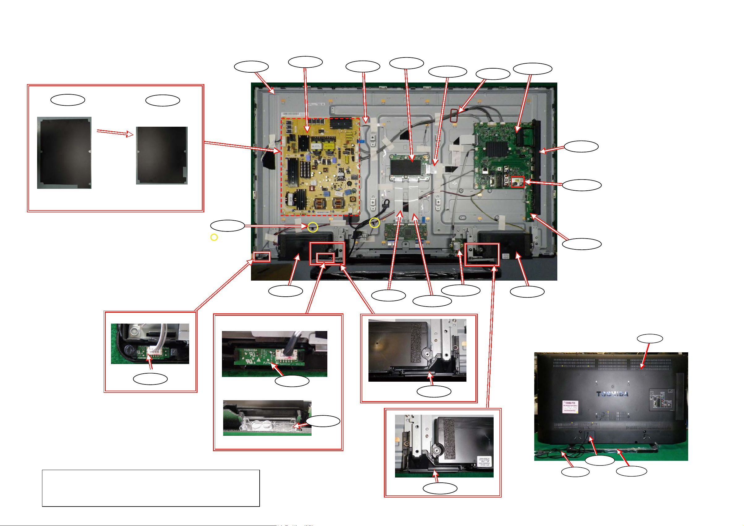
EXPLODED VIEW
(1/2)
A401S
P801x
A423S
A302
E02
(Under U800)
(Under E01)
mark
(2 places)
U04A is removed.
A201 is removed.
42L7453D/7463D series
Note:
These photographs are samples.
These photographs differ from the mass-production product.
Page 3
EXPLODED VIEW
(2/2)
42L7453D/42L7463D
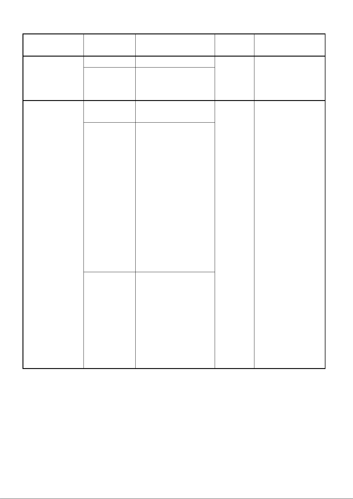
Location Service Part No. Description
A201 75036653 PIECE PIECE C R ASSY 14B J8, APRQ42J010E
A202 75036654 PIECE PIECE C L ASSY 14B J8, APRQ42J020E
A204 75036484 PIECE LENS RMT 55Z8, LENS RMT 55Z8, FCRR42J010E
A301 75037699 KEY PLATE ASSY, LCRR55D010E
A302 75036510 PIECE PIECE CORD POW 14B, PIECE CORD POW 14B, LCRR42J050E
A401S 75037685 COVER ASSY, UNIT (FOR SERVICE USE), 39C0GD51L02 For 7453D only
A401S 75037989 COVER ASSY, UNIT (FOR SERVICE USE), 39C0GD51L01 For 7463D only
A423S 75038497 STAND ASSY, AMRQ42J020E
B001 75037694 S-Fit LCD Panel (Open Cell, LGD LC420DUK-SGK2)
E01 75036525 SHEET INSULATOR POW F 4247Z8, ELRR42J010E
E02 75036526 SHEET INSULATOR POW B 4247Z8, ELRR42J020E
H7501 75037687 TUNER, SUT-RE232TN, PK31001480E For 7453D only
H7501 75037985 TUNER, SUT-PE232TN, PK31001510E For 7463D only
MZ01 75037698 CABLE, FFC, 51P-51P P0.5 L255, 12Z163, NBX5100170E
MZ02 75037696 CABLE, FFC, 51P-51P P0.5 L150, 12Z159, NBX5100160E
MZ03 75037697 CABLE, FFC, 41P-41P P0.5 L150, 12Z160, NBX4100190E
MZ04 75036544 CABLE, 42Z8 8P FFC, NBX0800050E
P801B 75023310 POWER CORD, EUROPE UK, 103025/2, GA04009190E For (B) model only
P801E 75022864 POWER CORD, EUROPE CONTINENT, 103025/3, RL833, GA02024150E For (G) model only
P801N 75022864 POWER CORD, EUROPE CONTINENT, 103025/3, RL833, GA02024150E For (N) model only
PP11 75037773 CLAMP/CLIP/WIRE SADDLE UAMS-05S-2, UAMS-0 5S-2
PP21 75021227 CLAMP, WIRE SADDLE, RBWS-1WM-V0 BK
U01A 75037676 PC BOARD ASSY, MAIN, A-BOARD, B911PE1168A1, 461C7851L02 For 7453D only
U01A 75037984 PC BOARD ASSY, MAIN(A-BOARD), B911PE1168B1, 461C7851L01 For 7463D only
U02A 75037656 PC BOARD ASSY, FRC, A-BOARD, B911PE1159A1, 465C4551L01
U03A 75037005 PCB LED UNIT Z8J8 COMPAL, B910PE1152B1, 455C4251L01
U04A 75037007 PCB RMT UNIT Z8J8 COMPAL, B912PE1153B1, 455C4351L01
U05A 75037657 PC BOARD ASSY, KEY, A-BOARD, B911PE1169A1, 454C5451L01
U800 75036527 POWER UNIT, PSLF226A01A, PK101W0541E
U802 75037695 MODULE, WIRELESS LAN, WLU5053-D4(ROHS) EU, PK29820020E
W661 75036482 SPEAKER, SPK-1561AJ, CG10150000E, PK23150000I
W662 75036482 SPEAKER, SPK-1561AJ, CG10150000E, PK23150000I
SAFETY PRECAUTION
The parts identified by mark are critical for safety. Replace only with part number specified.
The mounting position of replacement is to be identical with originals.
The substitute replacement par ts which do not have the same safety characteristics as s peci fied
in the parts list may create shock, fire or ot her haz ar ds .
Note:
Please see PPL put on Web PRESS for the newest information or other parts.
Page 4

PANEL IDENTIFICATION
A
Serial No. part printed on Rating Label
Panel Identification Code
Marking Marking Marking
BKT
CLU
DMV
ENW
FPX
GQY
HRZ
Panel Vendor
AUO
BriView
CMO
CHILIN
IPS
JS
Panel Vendor
SAMSUNG
LPL/LGD
CPT
Panel Vendor
SHARP
Page 5

REV. 00
Apr/16/2014
Page 6

SERVICE MANUAL
LCD Color Television
42L7453D/7463D series
(System Information)
Page 7

CONTENTS
1. IMPORTANT NOTICE
2. GREEN PRODUCT PROCUREMENT
3. LEAD-FREE SOLDER
4. SAFETY INSTRUCTION
5. SERVICE MODE
6. LED INDICATIONS FOR SERVICE
7. HOTEL MODE
8. MAIN BOARD EXCHANGE
9. WRITING SERIAL NUMBER INTO MAIN BOARD
10. INTERCONNECT
11. EXPLODED VIEW
12. SCHEMATIC DIAGRAM
1
Page 8

IMPORTANT NOTICE
WARNING:
You are requested that you shall not modify or alter the information or data provided
herein without prior written consent by Toshiba. Toshiba shall not be liable to
anybody for any damages, losses, expenses or costs, if any, incurred in connection
with or as a result of such modification or alteration.
THE INFORMATION OR DATA HEREIN SHALL BE PROVIDED "AS IS" WITHOUT ANY
WARRANTY OF ANY KIND, EITHER EXPRESS OR IMPLIED WARRANTY OF
MERCHANTABILITY AND FITNESS FOR A PARTICULAR PURPOSE.
Toshiba shall not be liable for any damages, losses, expenses or costs, if any,
incurred in connection with or as a result of use of any information or data provided
herein.
Page 9

GREEN PRODUCT PROCUREMENT
The EC is actively promoting the WEEE & RoHS Directives that define standards for
recycling and reuse of Waste Electrical and Electronic Equipment and for the Restriction of
the use of certain Hazardous Substances. From July 1, 2006, the RoHS Directive will
prohibit any marketing of new products containing the restricted substances.
Increasing attention is given to issues related to the global environmental. Toshiba
Corporation recognizes environmental protection as a key management tasks, and is doing
its utmost to enhance and improve the quality and scope of its environmental activities. In
line with this, Toshiba proactively promotes Green Procurement, and seeks to purchase
and use products, parts and materials that have low environmental impacts.
Green procurement of parts is not only confined to manufacture. The same green parts
used in manufacture must also be used as replacement parts.
LEAD-FREE SOLDER
This product is manufactured using lead-free solder as a part of a movement within the
consumer products industry at large to be environmentally responsible. Lead-free solder
must be used in the servicing and repair of this product.
WARNING: This product is manufactured using lead free solder.
DO NOT USE LEAD BASED SOLDER TO REPAIR THIS PRODUCT!
The melting temperature of lead-free solder is higher than that of leaded solder by 30ºC to
40ºC (54ºF to 72ºF). Use of a soldering iron designed for lead-based solders to repair
product made with lead-free solder may result in damage to the component and or PCB
being soldered. Great care should be made to ensure high-quality soldering when servicing
this product especially when soldering large components, through-hole pins, and on PCBs
as the level of heat required to melt lead-free solder is high.
Page 10

(1/4)
SAFETY INSTRUCTION
WARNING: BEFORE SERVICING THIS CHASSIS, READ THE "SAFETY PRECAUTION"
AND "PRODUCT SAFETY NOTICE" INSTRUCTIONS BELOW.
Safety Precaution
WARNING: SERVICING SHOULD NOT BE ATTEMPTED BY ANYONE UNFAMILIAR WITH
THE NECESSARY PRECAUTIONS ON THIS RECEIVER. THE FOLLOWING ARE THE
NECESSARY PRECAUTIONS TO BE OBSERVED BEFORE SERVICING THIS CHASSIS.
1. An isolation transformer should be connected in the power line between the receiver
and the AC line before any service is performed on the receiver.
2. Always disconnect the power plug before any disassembling of the product. It may
result in electrical shock.
3. When replacing a chassis in the cabinet, always be certain that all the protective
devices are put back in place, such as nonmetallic control knobs, insulating covers,
shields, isolation resistor-capacitor network, etc.
4. Always keep tools, components of the product, etc away from the children, These items
may cause injury to children.
5. Depending on the model, use an isolation transformer or wear suitable gloves when
servicing with the power on, and disconnect the power plug to avoid electrical shock
when replacing parts. In some cases, alternating current is also impressed in the
chassis, so electrical shock is possible if the chassis is contacted with the power on.
6. Always use the replacement parts specified for the particular model when making
repairs. The parts used in products require special safety characteristics such as
inflammability, voltage resistance, etc. therefore, use only replacement parts that have
these same characteristics. Use only the specified parts when the
in the circuit diagram or parts list.
7. Parts mounting and routing dressing of wirings should be the same as that used
originally. For safety purposes, insulating materials such as isolation tube or tape are
sometimes used and printed circuit boards are sometimes mounted floating. Also make
sure that wirings is routed and clamped to avoid parts that generate heat and which use
high voltage. Always follow the manufactured wiring routes / dressings.
mark is indicated
Page 11
(2/4)
8. Always ensure that all internal wirings are in accordance before re-assembling the
external casing after a repairing completed. Do not allow internal wiring to be pinched
by cabinets, panels, etc. Any error in reassembly or wiring can result in electrical
leakage, flame, etc., and may be hazardous.
9. NEVER remodel the product in any way. Remodeling can result in improper operation,
malfunction, or electrical leakage and flame, which may be hazardous.
10. Touch current check. (After completing the work, measure touch current to prevent an
electric shock.)
Plug the AC cord directly into the AC outlet. Do NOT use an isolation transformer for
this check.
Connect a measuring network for touch currents between each exposed metallic part
on the set and a good earth ground such as a water pipe.
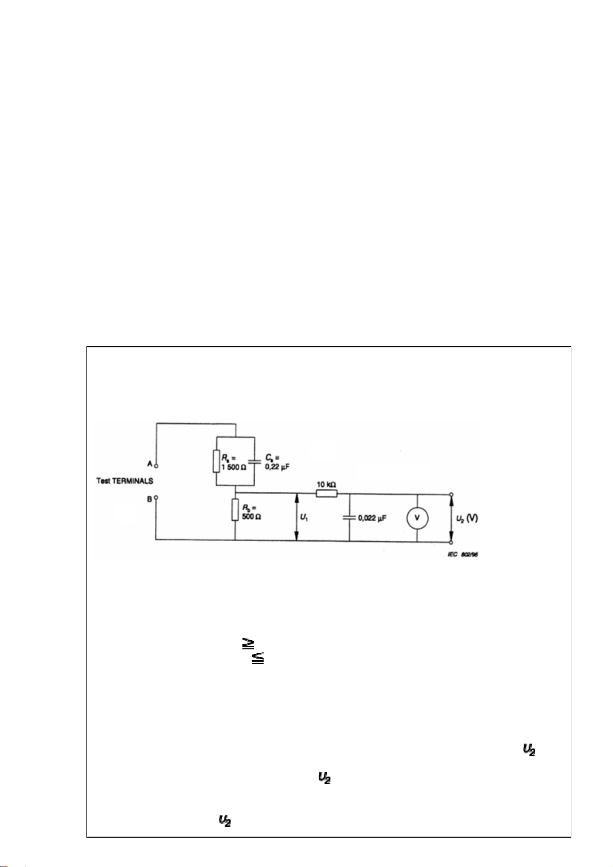
Annex D
(normative)
Measuring network for TOUCH CURRENTS
Resistance values in orms (Ω).
V: Voltmeter or oscilloscope
(r.m.s. or peak reading)
Input resistance :
1 MΩ
Input capacitance : 200 pF
Frequency range : 15 Hz to 1 MHz and d.c. respectively
Note: Appropriate measures should be taken to obtain the correct value in case of non
sinusoidal waveforms.
The measuring instrument is calibrated by comparing the frequency factor of with
the solid line in figure F.2 of IEC 60990 at various frequencies. A calibration curve is
constructed showing the deviation of
from the ideal curve as a function of
frequency.
TOUCH CURRENT =
/ 500 (peak value).
Page 12
(3/4)
The potential at any point (TOUCH CURRENT) expressed as voltage and does
not exceed the following value:
The part or contact of a TERMINAL is not HAZARDOUS LIVE if:
a) The open-circuit voltage should not exceed 35 V (peak) a.c. or 60 V d.c. or, if a) is
not met.
b)
The measurement of the TOUCH CURRENT shall be carried out in accordance
with IEC 60990, with the measuring network described in Annex D of this
standard.
The TOUCH CURRENT expressed as voltages and , does not exceed the
following values:
- for a.c. : = 35 V (peak) and = 0.35 V (peak);
- for d.c. : = 1.0 V
Note: The limit values of = 0.35 V (peak) for a.c. and = 1.0 V for d.c.
correspond to the values 0.7 mA (peak) a.c. and 2.0 mA d.c.
Page 13

(4/4)
Product Safety Notice
Many electrical and mechanical parts in this chassis have special safety-related characteristics.
These characteristics are often passed unnoticed by a visual inspection and the protection
afforded by them cannot necessarily be obtained by using replacement components rated for
higher voltage, wattage, etc. Replacement parts which have these special safety
characteristics are identified in this manual and its supplements; electrical components having
such features are identified by the international hazard symbols on the schematic diagram and
the parts list.
Before replacing any of these components, read the parts list in this manual carefully. The use
of substitute replacement parts which do not have the same safety characteristics as specified
in the parts list may create electrical shock, fire, or other hazards.
Page 14
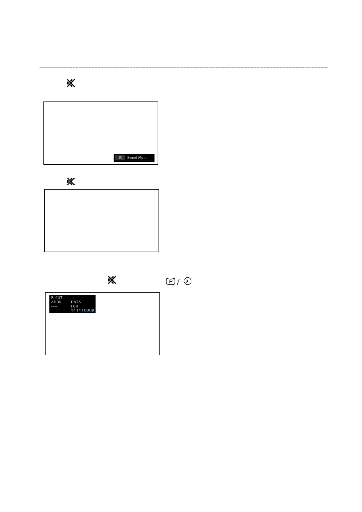
SERVICE MODE
ENTERING SERVICE MODE
1. Press button once on Remote Control.
TV mode changes as follows. Un-Mute => Mute
(1/3)
2. Press
button again and keep pressing.
(Sound Mute is canceled)
3. While pressing the
butt on, press button on TV control panel.
S
(Enter Service Mode)
Page 15
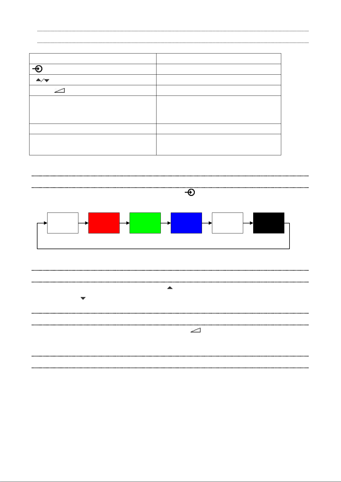
KEY FUNCTION IN THE SERVICE MODE
Normal
The following key entry during display of adjustment menu provides special functions.
Button Function
(2/3)
button (on Remote)
P (on Remote) Selection of the adjustment items
Volume +/– (on Remote) Change of the data value
[7] button Automatic A/D Adjustment
[9] button Self Check display ON
[Exit] button Exit from Service mode
CAUTION: Never try to perform initialization unless you have changed the memory IC.
Test signal selection
(PC, Component, Composite(PAL, NTSC))
Self Check display Off
TEST SIGNAL SELECTION
1) While displaying the adjustment menu, every pressing of button on the Remote Control changes the
built-in test patterns on screen as described below.
Picture
Red screen Green screen
Blue screen
When a pattern is changed at the time of an ATV display, it can display only for a moment.
SELECTING THE ADJUSTING ITEMS
1) While displaying the adjustment menu, press the P button to cycle through the adjustment items in the
order of table. (P
button for reverse order)
ADJUSTING THE DATA
1) While displaying the adjustment menu, press the VOLUME +/– button to change the value of data in
the range from 00H to FFH. The variable range depends on the adjusting item.
EXIT FROM SERVICE MODE
1) Press the [Exit] button on Remote.
Page 16

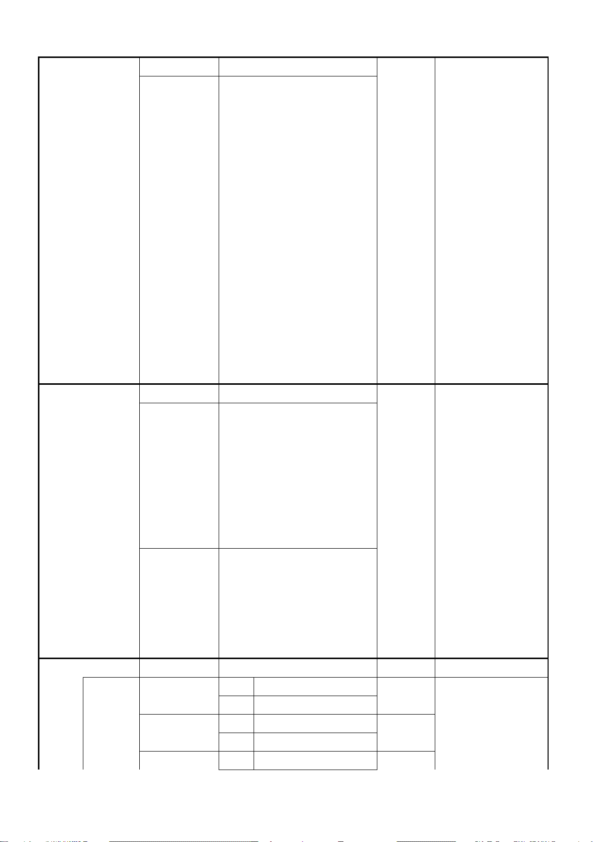
ADJUSTING ITEMS IN THE SERVICE MODE
Item Description
RCUT RED CUTOFF
GCUT GREEN CUTOFF
BCUT BLUE CUTOFF
RDRV RED DRIVE
GDRV GREEN DRIVE
BDRV BLUE DRIVE
OSRC COOL R-CUTOFF-OFFSET for COOL
OSRC NATURAL R-CUTOFF-OFFSET for NATURAL
OSRC WARM R-CUTOFF-OFFSET for WARM
OSGC COOL G-CUTOFF-OFFSET for COOL
OSGC NATURAL G-CUTOFF-OFFSET for NATURAL
OSGC WARM G-CUTOFF-OFFSET for WARM
(3/3)
OSBC COOL B-CUTOFF-OFFSET for COOL
OSBC NATURAL B-CUTOFF-OFFSET for NATURAL
OSBC WARM B-CUTOFF-OFFSET for WARM
OSRD COOL R-DRIVE-OFFSET for COOL
OSRD NATURAL R-DRIVE-OFFSET for NATURAL
OSRD WARM R-DRIVE-OFFSET for WARM
OSGD COOL G-DRIVE-OFFSET for COOL
OSGD NATURAL G-DRIVE-OFFSET for NATURAL
OSGD WARM G-DRIVE-OFFSET for WARM
OSBD COOL B-DRIVE-OFFSET for COOL
OSBD NATURAL B-DRIVE-OFFSET for NATURAL
OSBD WARM B-DRIVE-OFFSET for WARM
OSRD 3D COOL R-DRIVE-OFFSET for COOL (3D)
OSRD 3D NATURAL R-DRIVE-OFFSET for NATURAL (3D)
OSRD 3D WARM R-DRIVE-OFFSET for WARM (3D)
OSGD 3D COOL G-DRIVE-OFFSET for COOL (3D)
OSGD 3D NATURAL G-DRIVE-OFFSET for NATURAL (3D)
OSGD 3D WARM G-DRIVE-OFFSET for WARM (3D)
OSBD 3D COOL B-DRIVE-OFFSET for COOL (3D)
OSBD 3D NATURAL B-DRIVE-OFFSET for NATURAL (3D)
OSBD 3D WARM B-DRIVE-OFFSET for WARM (3D)
Page 17
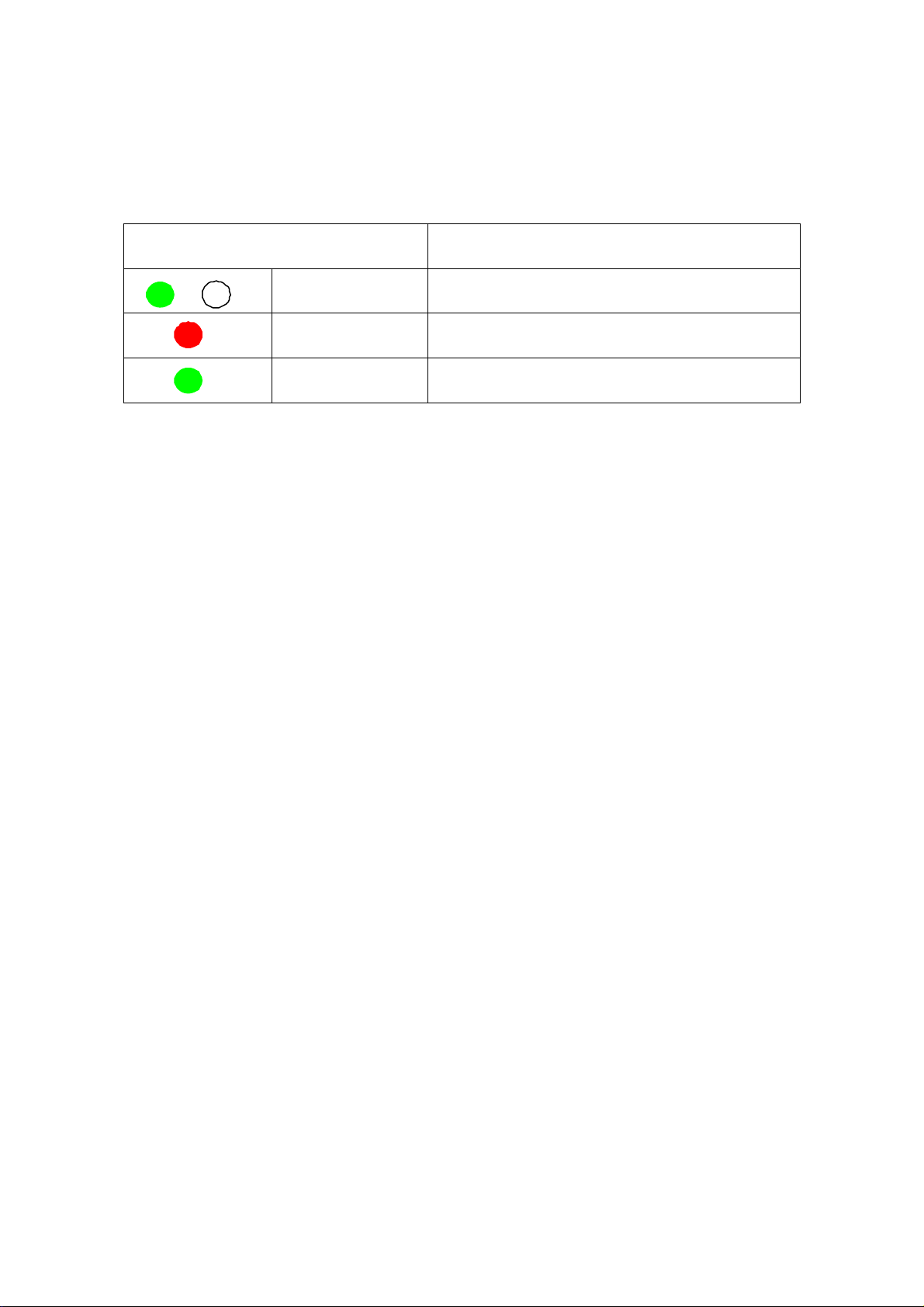
LED INDICATIONS FOR SERVICE
SW Upgrade and Error conditions indicated by the Power LED is described below.
Power LED
/
Green blink SW Upgrade in Progress
Red SW Upgrade Failed
Green SW Upgrade Successful
Page 18
(1/18)
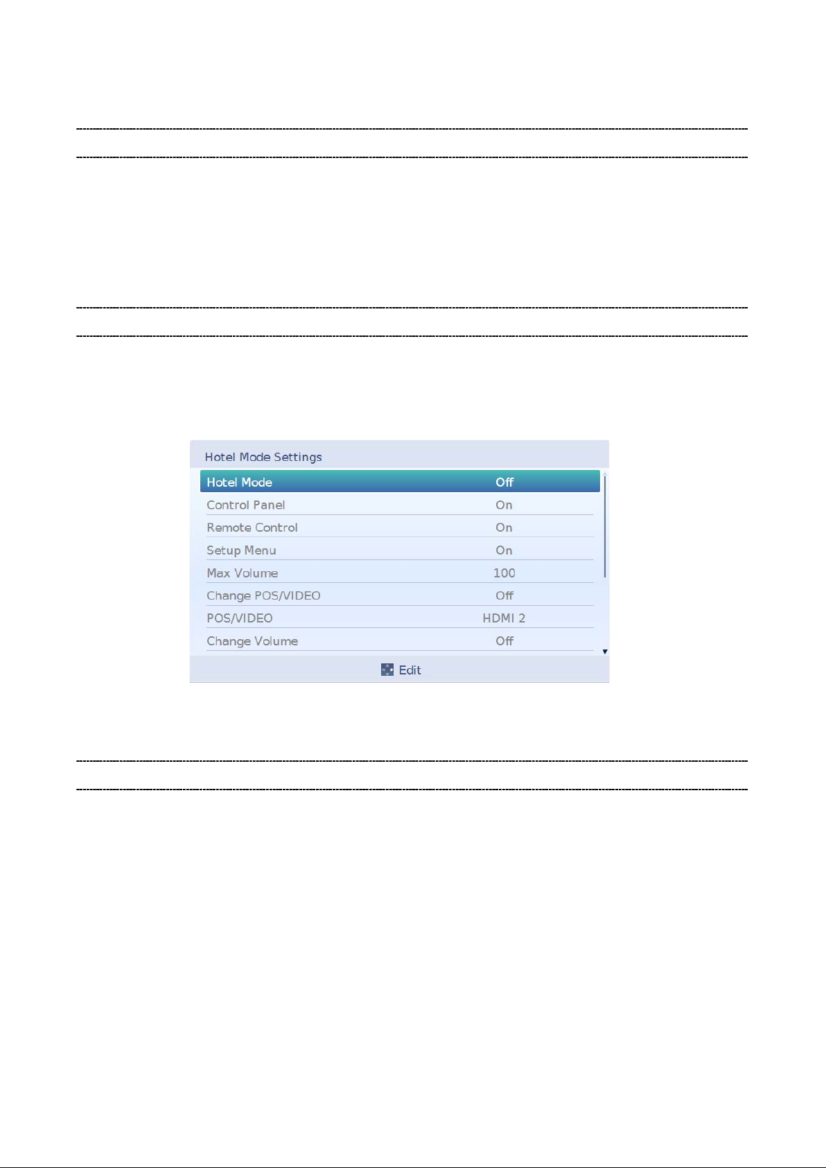
HOTEL MODE
1. ENTERING HOTEL MODE MENU
Hotel Mode Menu should be shown by the following operation.
1) Open Main Menu by pressing Menu but t on of RCU.
2) Press the following password nu mb er “1048” with the button of Remote Control.
Note: Hotel Menu can be displayed to in put t he pass word nu mber when ther e is focus in the f irst lay er of
Main Menu.
2. DISPLAY OF HOTEL MODE MENU
- The Graphic Design and color of Hotel Mode Menu is the same as the User menu.
(Small differences which do not affect to operation will be acceptable)
- The language will fol low the “Menu Language” setti ng in t he menu
(Fig.1; Example of Menu Image)
3. OPERATING HOTEL MODE MENU
- To enable Hotel Mode, press ▲/▼buttons to select “Hot el Mode” item and press button.
Press ▲/▼buttons to select “On” and press OK button.
- Once Hotel Mode is “On”, the Hotel Mode settings will be en abl ed f or adjusting.
- Press ▲/▼ buttons to select item of Hotel Mode Settings.
Press and ▲/▼ buttons to select settings a nd press OK button.
See the table below for explanation of each setting.
- Press Exit when finished adjusting the settings.
Page 19
(2/18)
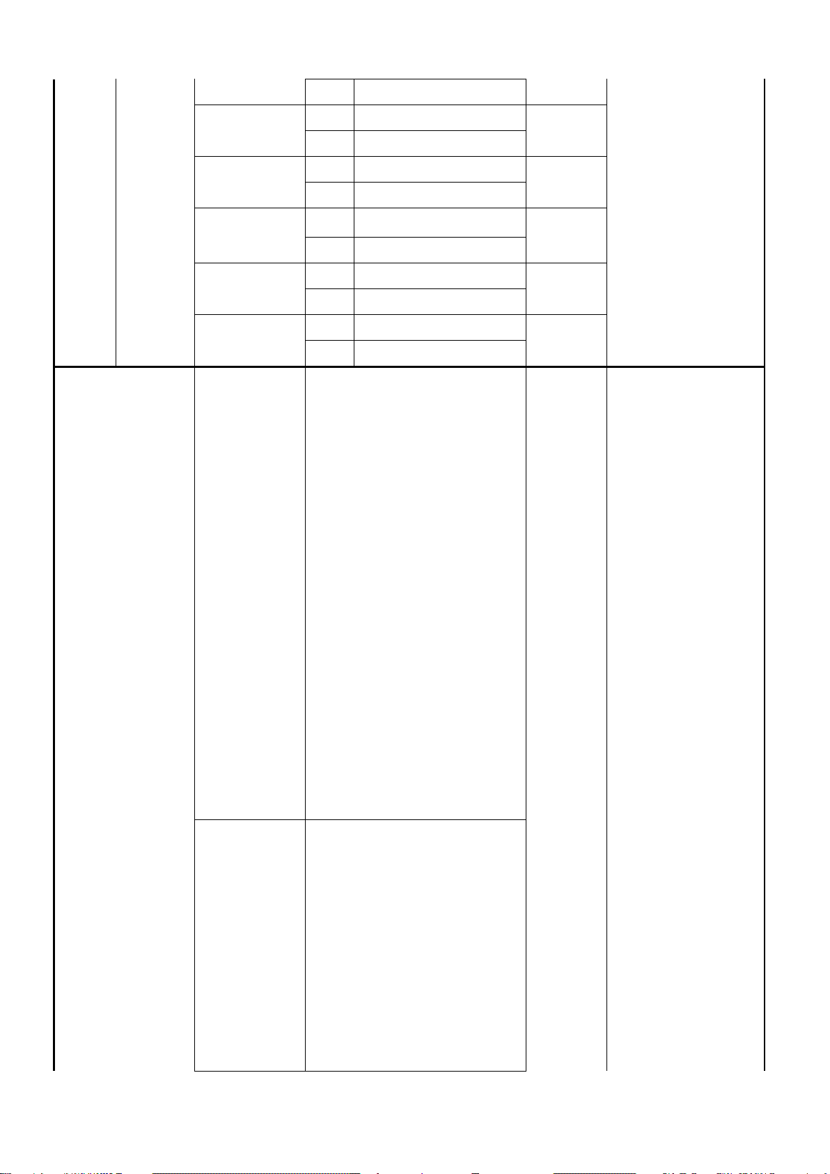
Item Options Description
Hotel Mode On Enable Hotel Mode Off -
Off Disable Hotel Mode.
All the settings of Hotel Mode
are disabled.
Control Panel On Allow use of all Control panel
buttons
Off (All Functions) Prohibit use of all control panel
buttons.
But, Power Off -> On by contro l
panel POWER button is not
prohibited.
(Power On -> Off is prohibited.)
Moreover, TV can be rebooted
by a long pressing (4 seconds
Factory
settings
On - Grayed out when "Hotel
Gray Out Conditions
Mode" = [Off]
Off (All except
power)
or more) of the control panel
power button.
* Entering Service mode/Hotel
mode Menu is not prohibited.
* Control panel buttons are
available during Service mode.
Prohibit use of all control panel
buttons.
But, Power On/Off by control
panel POWER button is not
prohibited.
* Entering Service mode/Hotel
mode Menu is not prohibited.
* Control panel buttons are
available during Service mode.
Page 20
(3/18)
Remote Control On Enable the remote control buttons. On - Grayed out when "Hotel
Off Disable the remote control buttons.
* The following remote codes are
not disabled.
- Super User mode (40BFFE)
- S mode (40EEC3)
* If “Off" is selected, RCU will not
function in any menu (including
no menu) except Hotel Menu. To
turn this option “On” later, “Hotel
Menu shortcut” (MENU-1-0-4-8)
can be used to pop up Hotel
Menu.
* TV can be rebooted by a long
pressing (4 seconds or more) of the
Remote control power button.
* Remote Enabled during Service
mode/Hotel mode Menu.
Mode" = [Off]
Setup Menu On Allow access to Main menu On - Grayed out when "Hotel
Off Prohibi t access to Main menu.
Main menu is grayed out and it is
prohibited to select.
Mode" = [Off]
* If “Off" is selected, Main menu
will not function. To turn this
option “On” later, “Hotel Menu
shortcut” (MENU-1-0-4-8) can be
used to pop up Hotel Men u .
Off (Except
Language)
OSD Menu Control
Prohibit access to all items in Main
menu except for the Language
setting.
The prohibited items are not shown
on the menu. (Gray-out instead of
erasing is acceptable)
(2nd layer) Picture On Enable Picture Menu On - Grayed out when "Hotel
Off Disable Picture Menu
Sound On Enable Sound Menu On
Off Disable Sound Menu
Options On Enable Option Menu On
Mode" = [Off]
Page 21
Off Disable Option Menu
Installation On Enable Installation Menu On
Off Disable Installation Menu
Network On Enable Network Menu On
Off Disable Network Menu
3D On Enable 3D Menu On
Off Disable 3D Menu
Timers On Enable Timers Menu On
Off Disable Timers Menu
Get Help On Enable Get Help Menu On
Off Disable Get Help Menu
(4/18)
Welcome Screen
(*Boot-up Ad is
unsupported in the
hotel mode.)
On When Hotel Mode is “On”, display a
fixed welcome image dur ing a bout 5
seconds to the center (without
expanding) every time the TV is
switched on.
*When Welcome Screen is “On”,
display a welcome image in no signal
too.
* Welcome image can be changed
through USB Clone Function. A
default welcome image (TOSHIBA) is
available. Refer to 4.1 for details of
Welcome image.
Welcome image becomes default by
“Reset Hotel Menu”
(*But Welcome image don’t becomes
default by USB Live Update, Network
On (AC) - Grayed out when "Hotel
Mode" = [Off]
Upgrade and OAD.)
On (AC) When Hotel Mode is “On”, display a
fixed welcome image dur ing a bout 5
seconds to the center (without
expanding) when TV power on first at
AC power is applied.
*When Welcome Screen is “On”,
display a welcome image in no signal
too.
* Welcome image can be changed
through USB Clone Function. A
Page 22
default welcome image (TOSHIBA) is
available. Refer to 4.1 for details of
Welcome image.
Welcome image becomes default by
“Reset Hotel Menu”
(*But Welcome image don’t becomes
default by USB Live Update, Network
Upgrade and OAD.)
Off Not display a welcome image every
time the TV is switched on and only
when TV power on first at AC power
is applied.
Also not display a welcome image in
no signal.
(5/18)
Signal Lost Message
(*Only available when
“Welcome Screen” is
[On].)
Time Information
Channel
On If there is no signal the same
welcome image is displayed during
about 5 seconds to the center
(without expanding), when “Welcome
Screen” is set to “On”.
On the bottom side of image there i s a
message (OSD message) displaying
“No Signal”.
Off If there is no signal the same
welcome image is displayed during
about 5 seconds to the center
(without expanding), when “Welcome
Screen” is set to “On”. And not
display a message “No Signal”.
0-9999 Witho ut time infor mat ion when "On
Timer" of the Main menu is set, time
On
(* When
“Welcome
Screen" is
set to “Off”,
Signal Lost
Message is
forced
“On”.)
0 - Grayed out when "Hotel
- Grayed out when "Hotel
Mode" = [Off]
- Grayed out when
"Welcome Screen " =
[Off]
Mode" = [Off]
information is acquired from the
specified channel.
* When time information is acquired,
"On Timer" can be set.
(Timeout of acquisition is 30
seconds.) (Fig.3)
Change POS/VIDEO On TV tunes to preset “POS/VIDEO”
(channel or input) when TV is
powered on.
Off - Grayed out when "Hotel
Mode" = [Off]
Page 23
On (AC) TV tunes to preset “POS/VIDEO”
(channel or input) only when AC
power is applied.
When TV is powered on by power
button, tune to the last channel or
input.
Off TV Tunes to the last chan nel o r input
viewed when powered on
(6/18)
POS/INPUT/VIDEO
(*Only available when
“Change POS/VIDEO”
is [On].
*The satellite is not
included in this
selection.)
* The input which does
not exist on the model
should not be shown.
(eg. “DTV” is not
shown on ATV
models.)
ATV/DTV POS
(*Only available when
"POS/INPUT/VIDEO"
is ATV or DTV.)
ATV ATV ATV - Grayed out when Hotel
DTV DTV
EXT1 EXT1
EXT2 EXT2
EXT3 EXT3
HDMI1 HDMI1
HDMI2 HDMI2
HDMI3 HDMI3
HDMI4 HDMI4
PC PC
ATV 0-99 0 - Grayed out when Hotel
DTV Number of chan nel li st
*The channel not acquired is not set.
(The value is not preserved and
The first
number of
channel list
Mode = [Off]
- Grayed out when
"Change POS/VIDEO" =
[Off]
Mode = [Off]
- Grayed out when
"POS/INPUT/VIDEO" =
returns to the origin when the
channel not acquired is set.)
*A set value returns to default after
the Auto/Manual tuning.
*A set value returns to default if the
set channel is deleted.
*A set value returns to default if
Channels-Renumber is executed.
* If the same channel number as
(1)TV Channels, (2) Radio Channels
and (3)Text Channels in DTV exist, it
is set by the priority level of (1), (2),
and (3).
SCART Pin8 On Pin8 will go on normal operation. On - Grayed out when "Hotel
Off Pin8 is ignored.
not [ATV/DTV]
- (For Only DTV) Grayed
out when there is no
acquisition channel in the
DTV channel list
Mode" = [Off]
Page 24

(7/18)
Grayed out when "USB
USB Control On USB function available On - Grayed out when "Hotel
Off USB function not available but allow
USB bus power
*USB Control is off will make “USB
Live Upgrade” and “AC on USB
upgrade” disabled too.
USB Power On USB bus power is supplied. On
100 - Grayed out when "Hotel
Volume Control
(Only available when
“Fixed Volume” is Off.)
Max Volume
Off USB bus power is not supplied.
(USB Flash drive doesn't work)
*
USB power is off will make “USB
Live Upgrade” and “AC on USB
upgrade” disabled too.
On Enable Volume Control Off - Grayed out when "Hotel
Off Disable Volume Control
0-100 Set maximum volume level.
Mode" = [Off]
Power" = [Off]
- Grayed out when "Hotel
Mode" = [Off]
Mode" = [Off]
- Grayed out when "Fixed
Volume" = [On]
(Only available when
“Volume Control” is
On.)
Startup Volume
(Only available when
“Fixed Volume” is Off.)
Volume Value
(Only available when
“Startup Volume” is
On.)
Fixed Volume On TV volume level is forced to “Fixed
On TV volume level is f or ced to “ V olum e”
Off TV volume level does not change
0-100 Volume level when TV is powered
It limits the volume level which can
be set by Volume button.
If you set it to 70, Volume bar can not
go to 71 or higher.
level when TV is powered on
when TV powers on
on.
This volume level can be set by Max
Volume or less.
Mode" = [Off]
- Grayed out when
"Volume Control" = [Off]
- Grayed out when "Fixed
Volume" = [On]
Off - Grayed out when "Hotel
Mode" = [Off]
- Grayed out when "Fixed
Volume" = [On]
30 - Grayed out when "Hotel
Mode" = [Off]
- Grayed out when
"Startup Volume" = [Off]
- Grayed out when "Fixed
Volume" = [On]
Off - Grayed out when "Hotel
Fixed Volume Value
(Only available when
“Fixed Volume” is On.)
Volume Value” level.
Off TV volume level is not forced to
“Fixed Volume Value” level..
0-100 Sets the fixed value the volume can
have. If Fixed Volume Limit is ON,
volume is set with the value here.
Mode" = [Off]
30 - Grayed out when "Hotel
Mode" = [Off]
- Grayed out when "Fixed
Page 25
Volume" = [Off]
(8/18)
Change Picture Mode
(Only available when
“Menu Control /
Picture" is On.)
Fixed Picture Mode
(Only available when
“Change Picture
Mode” is On.)
Change Picture Size On This item allows the picture mode to
On Picture setting mode is forced to
“Fixed Picture Mode” mode.
“Main menu/Picture Mode”, “Quick
menu/Picture Mode” and
“RCU/select picture mode button” will
be inaccessible.
Off Normal operation
AutoView AutoView Standard - Grayed out when "Hotel
Dynamic Dynamic
Standard Standard
Hollywood Night Hollywood Night
Hollywood Day Hollywood Day
Hollywood Pro Hollywood Pro
be set to a specific size (16:9, 4:3
etc) and prevents adjustment by the
Off - Grayed out when "Hotel
Mode" = [Off]
Mode" = [Off]
- Grayed out when
"Change Picture Mode"
= [Off]
Off - Grayed out when "Hotel
Mode" = [Off]
end-user.
“Quick menu/Picture Size” and
“RCU/select picture size button” will
be inaccessible.
Off Normal operation
Fixed Picture Size
(Only available when
“Change Picture Size”
is On.)
TV Power Disabled TV returns to previous Standby/On
Wide Wide Wide - Grayed out when "Hotel
4:3 4:3
Super live Super live
Cinema Cinema
State when AC power is applied
Force On Power TV on when AC power is
applied
Force Standby Put TV in Standby when AC power is
applied
Mode" = [Off]
- Grayed out when
"Change Picture Size" =
[Off]
Disabled - Grayed out when "Hotel
Mode" = [Off]
Note:
- When the “Active Standby Mode” is
set to “On”, the standby mode is
“Active Standby”.
- When the “Active Standby Mode”
Page 26

is set to “Off” and the “Wake on LAN
*When the Hotel Mode is On, this
*When the Hotel Mode is On, this
setting becomes effective regardless
eletext (or
Standby Mode” is set to “On”, the
standby mode is “WoL Standby”.
- When “Active Standby Mode” and
“Wake on LAN Standby Mode” are
set to “Off”, the standby mode is
“Standby”.
(9/18)
Hybrid TV Standard Enabled Enables the use of Hybrid TV
setting becomes effective regardless
of the setting of the main menu.
Disabled Disables the use of Hybrid TV
of the setting of the main menu.
Teletext On Enables the use Teletext (or MHEG if
available).
Off Disables the use of T
MHEG)
Position Change on
HDMI Input
On RF tuning via P▲, P▼, RETURN,
and number buttons is allowed.
(Normal operation)
Off When viewing HDMI input, RF tuning
Enabled - Grayed out when "Hotel
Mode" = [Off]
On - Grayed out when "Hotel
Mode" = [Off]
On - Grayed out when "Hotel
Mode" = [Off]
via P▲, P▼, RETURN, and number
buttons is disabled
A/D Channel List On TV shall combine both Analogue &
Digital channels in one channel list
(Fig.2), and select the ATV/DTV
channel without boarder.
* RF tuning without border via P▲, P
▼, Previous channel
Off DTV Channel List and ATV DTV
Channel List are separated.
NIT Update On Normal operation On - Grayed out when "Hotel
Off Disable Network Information Table
(NIT) update
Disable Standby Channel update and
Dynamic Scan
Off - Grayed out when "Hotel
Mode" = [Off]
Mode" = [Off]
Page 27
(10/18)
Start USB
Grayed out when "USB
Grayed out when
USB Clone Function Start USB Clone Press “OK” on "Start USB Clone"
button, USB Clone mode initial
window is displayed.
* Refer to “4. USB CLONE
FUNCTION”
Reset Hotel Menu When select this item, displ ay “Are
you sure you want to reset to default
settings? (Yes/No (Default:No))”
message.
If select Yes, reset Hotel Menu
settings to default values. And
welcome image becomes default,
too.
* Hotel Menu settings should not be
reset by “Reset TV” on the Main
menu.
(To prevent users from cancelling
- Grayed out when "Hotel
Clone
- Grayed out when "Hotel
Mode" = [Off]
Power" = [Off]
Mode" = [Off]
Hotel Menu settings that have been
specially set by the hotel)
Signage Mode On Enable Signage Mode Off - Grayed out when "Hotel
Off Disable Signage Mode.
All the settings of Signage Mode are
disabled.
Signage Mode Setup -
(2nd layer) Operational
mode
Online Display the homepage of
the assigned URL by Full
Screen Mode of Open
Browser, when turning on
DTV. If assigned URL is not
registered, display the
current Open Browser’s
homepage by Full Screen
Online
Mode" = [Off]
"Signage Mode" = [Off]
Mode, when turning on TV.
*Display error message
“Network unavailable.
Please check your Internet
connection”, when DTV is
not connected to the
network.
Page 28
*Tuner screen (etc.) is not
Grayed out when
" =
" =
displayed from power On to
the contents playback as
much as possible.
Offline Playback contents in USB
memory inserted in DTV by
Media Player without
confirmation message,
when turning on DTV.
In addition, playback
contents in USB memory by
Media Player without
confirmation message,
when USB memory is
inserted during power On of
DTV.
(11/18)
URL setting
mode
*Tuner screen (etc.) is not
displayed from power On to
the contents playback as
much as possible.
Press [OK] key, display the
URL input popup (ex.
Network Name of Manual
Setup in Network Setup).
Input the text of URL by
software keyboard of DTV.
Select [Done] button in
popup, set to assigned
default URL of Open
Browser for Signage mode.
* The text limited with URL
cannot be used.
* Assigned default URL of
"Operational mode
[Offline]
Playback
Content
Open Browser for Signage
mode can be copied with
the USB clone Function.
Photo Photo contents in root of
USB memory are selected
and play back.
In case of no playback
Photo - Grayed out when
"Operational mode
[Online]
Page 29
content, display ERROR
Grayed out when
" =
Grayed out when
" =
Grayed out when
t" =
Grayed out when
" =
Grayed out when
"Playback Content" =
“Unsupported file”.
And return the Photo List to
root of USB memory.
Video Video contents in root of
USB memory are selected
and play back.
In case of no playback
content, display ERROR
“Unsupported file”.
And return the Video List to
root of USB memory.
(12/18)
Repeat playback On Repeat playback contents
automatically (Photo:
Slideshow
Video: Repeat all)
*It is repeat playback
according to the list of
Media player.
Off No repeat playback
contents.
Interval time of
Slideshow
(Photo Mode)
Background
Music (Photo
3,5,10,
15,30,
60,90
sec
On Enable playback of the
Select the desired interval
time of Slideshow on Photo
mode. (The value is set
independently of current
Media Player interval time.)
BGM (background music) in
Off -
"Operational mode
[Online]
5sec -
"Operational mode
[Online]
"Playback Conten
[Video]
Off -
"Operational mode
Mode)
root of USB memory during
Photo playback mode.
Playback of the BGM is
followed to current Media
Player.
Off Disable the BGM
[Online]
-
[Video]
Page 30
Reset Signage
When select this item,
(13/18)
Menu
display “Are you sure you
want to reset to default
settings? (Yes/No
(Default:No))” message.
If select Yes, set to default
all setting in Signage Mode
Menu
* Signage Menu settings
should not be reset by
“Reset TV” on the Main
menu and “Reset Hotel
Menu”.
Page 31

Explanation of AD Channel List
DTV Mode ATV Mode
DTV Mode ATV Mode
DTV Mode ATV Mode
DTV Mode ATV Mode
A/D Channel List
= Off A/D Channel List = On
Press [LIST] key Press [LIST] key
Press [LIST] key
Press [LIST] key
DTV Channel List
(All Channels)
ATV Channel List ATV and DTV Channel List
(All Channels or TV Channels)
Note:
Yes
No
Explanation of Time Information Channel
(Fig.2)
(14/18)
- DTV Channel List: Upper side
- ATV Channel List: Lower side
- The focus is on the current channel.
This flow is applied to Time Information Channel of the Hotel Mode.
When the setting of “On
Timer” is started.
Can TV receive DTV
broadcast info
(TDT/TOT)?
Is “Enable DTV Clock”
set to [On]?
"On Timer" can use
"Power On T ime".
Yes
No
Yes
Is the Time Information
Channel set?
Yes
Get Time information from
the set channel.
Was time information able to
be acquired?
(Fig.3)
No (Timeout 30sec)
No
No
“On Timer” can use “Time
until Power On”.
Page 32

(15/18)
4. USB CLONE FUNCTION
4.1. Feature overview
Hotel Menu settings and Wel co me Scre en i mage, Pictur e set ting s, Default URL of T osh iba Cloud TV
Services and Networ k settings should be copied to other TV by Hotel Menu “USB Clone Function”.
< Welcome Screen image >
・File name: WelcomeScreen.jpg (case sensitive)
・File type: JPEG
・Color depth: 24bpp
・Resolution: 1280 x 720
・File size: 1MB or less
Note: The Welcome image is preserved besides the TOSHIBA logo (default). W hen user would like to
copy Welcome Screen, the clone data should be exported to USB memory in advance and then put the
Welcome Screen i mag e in to USB and start import Clone data from USB to TV.
< Default URL of Toshiba Cloud TV Services >
・File name: hotelCloudConf ig.txt (case sensitive)
*However, URL can be op er ated on the site specially developed.
・File type: Text
Note: When user would like to copy “URL o f Toshiba Cloud TV Services”, the clone data should be
exported to USB memory in advance and then put “
Clone data from USB to TV.
4.2. Copying data f or m TV to USB
(1) Press “OK” on “Start USB Clone” button of “USB Clone Function”, U SB Cl one mode initial window
[1-1] is displayed.
The options below are selected by left and right keys in this window.
USB to TV Copy setting data in USB mem or y to TV
TV to USB Copy TV settings to USB memory
(2) Insert USB memory, select “TV to USB” [1-2] and press [OK] key.
hotelCloudConfig.txt” file into USB and start import
(3) The now copying wind ow [1-3] will be displayed.
(4) Wait for wind ow that indicates the copying process is complete before remov ing t he U SB drive.
Page 33

Note: The title of the scr een image changes to USB Clone.
Complete copy
Error
[1-1]
(16/18)
[1-2]
OK key
[1-3]
Page 34

(17/18)
4.3. To write data form USB to TV
(1) Press “OK” on “Start USB Clone” button of “USB Cl one Func tion”, USB Clone mode initial window
[2-1] is displayed.
(2) Insert USB memory, select USB to TV [2-1], and press [OK] key.
(3) The window [2-3] w ill be displayed.
(4) W hen the copying has finished successfully, the message "The TV will reboot when this window is
closed." will be displayed. If the copying is not successful, an er r or message will be displayed.
(5) Exit the menu and the TV w i ll reboot.
(6) Remove the USB memory.
Page 35

Up and
Right and
Complete copy
Note: The title of the scr een image changes to USB Clone.
[2-1]
Down key
(18/18)
[2-2]
[2-3]
[2-4]
Left key
OK key
Error
[2-5]
Restart power
EXIT key
Page 36

(1/3)
[Example] Model_Setting_L6453_32_L.bin
TV series
Panel size
Panel Vendor
MAIN BOARD EXCHANGE
When Main board is ex changed, t he Ap plicati on S W (Firrmware) and Model Setting need t o
be updated and the serial number needs to be written the serial number into Main Board
(see “WRITING SERIAL NUMBER INTO MAIN BOARD”).
Please update in the following procedures.
Updating of Software and Model Setting
1. Copy the Application SW (Firmware) file and the Model Setting file to the root of the USB
mass storage device.
Application SW:
[Example] UPDATE_EU14_8.1.56.00.01.1_INIT_CLEAR#.enc
This Application SW is for all of
L74/L64 models.
This number is
an example.
“enc” means encrypted .
This SW is encrypted for
security.
Model Setting File:
Model setting files are categorized by shipout.
Each Shipout folder contains model setting files.
Page 37

2. Unplug TV, and then Insert the USB mass storage device to the USB slot of the TV.
3. Plug TV.
Software updating starts.
If Software updating does not start and the front LED lights red, then press [Power] key on
Remote Control to start Software updating.
4. After updating complete, unplug TV and remove the USB mass storage device.
(2/3)
5. Plug TV, then check the updating by using self check screen.
Refer to “Confirmation of Software updating” section on next page.
6. Update t o the newest SW.
This model can be updated from aerial or network to the newest Software.
Refer to the user manual of this model for the updating method.
Page 38

Confirmation of Software updating
TV model and
Panel vendor
[The 4th number and Shipout]
14 Nordic (N)
Check the TV Model and Model Info by using self check screen.
1. Press SETUP on Remote Control.
2. Select “Get Help” >> “System Information”
3. Press “3” “5” “7” “4”
(3/3)
Self check screen is displayed.
10 UK&Ireland (B)
12 Continental(France is included) (G)
13 Ru ssia (R)
Page 39

(1/2)
WRITING SERIAL NUMBER INTO M AIN BOARD
When the board is broken, service man will go to customers home and change the board. After
change the board service man has to put the serial number same as before. So the servi ce man will
use the PC and write the serial number to USB mass storage device. After that the service man will
plug the USB mass storage device to the TV and write the serial number to the TV.
1. Create the ini file by Text Editor.
File Name: ServiceSerialNumberWriting.ini
File Format: Plain Text
Write two lines, "[serial number]" and a serial number, using the text editor on Windows.
For example, when a serial number is "C37222T00008L1":
[serial number]
C37222T00008L1
2. Use the USB mass storage device formatted with “FAT32”.
3. Copy the "ServiceSerialNumberWriting.ini" file to the root directory of the USB mass
storage device.
4. Enter Service mode.
1. Press button once on Remote Control.
TV mode changes as follows. Un-Mute => Mute
2. Press
3. While pressing the
button aga in and keep pres sing.
button, press button on TV control panel.
5. Inser t the USB mass storage device to the USB slot of the TV set.
Writing starts.
Page 40

6. After fini sh writing the “OK” and “Serial number” appear on TV.
OK!!
Serial No: C35244C00001D1
7. Unplug USB mass storage device.
8. Check the serial number by using self check screen.
How to enter the self check screen.
1 Press SETUP on remote control unit.
2 Select “Get Help” >> “System Information”
3 Press “3” “5” “7” “4”
(2/2)
Page 41

Wiring Diagram (42/47L7453D/7463D series)
CN650 CN1 CN505 CN502 CN506
CN741 1 1 Anode1 1 1 1
2
RMT_IN
2
C_IRIN 3 3
Anode2
3 3 3
4
OP_IN
4
C_OP_IN 5 5
Anode3
5 5 5
11
Anode6
11 11 11
12 12
Cathode6
12 12 12
13
Anode7
13 13 13
2
GND 14 14
Cathode7
CN3 14 14 14
4
RED 16 CN90 PJ90 2
PWM_2
16 16 16
20 4 12V 4 12V 6
PWM_6
20 20 20
CN300 24 8 GND 8 GND 24 24 24
11 GND 11 GND_SOUND 27 27 27
29 P801A 29 29 29
30 CN91 PJ91 1 L 30 30 30
2 N 31 31 31
CN743 35 5 NC 5 18V_LNB 35 35 35
2
C_KEY_1
2
C_KEY_1 37 7 B_BL_ONOFF 7 BL_ON/OFF 37 37 37
42 42 42
CN162 44 44 44
2
M_USB0DM
2
M_USB0DM 46 CN782 CN501 46 46
5
M_WWOL_WAKEUP
5
M_WWOL_WAKEUP 49
3
GND
3
GND 49 49
RMT
Speaker(L)
LED board
KEY board
WiFi module
P801x
U04A
U03A
U05A
U802
U01A
U800
U02A
Panel
T-CON
MZ04
1 3.3V_TVM 1 3.3V_STB 2 2
3 GND 3 GND 4 4
5 3.3VF 5 3.3V_VD 6 6
6 5V1 7 7
7 GND 8 8
8 C_LED G 9 9
9 C_LED R 10 10
11
1 5V1 13
3 Green 15 1 PWM_1 15 15 15
17 1 12V 1 12V 3
18 2 12V 2 12V 4
19 3 12V 3 12V 5
21 5 GND 5 GND 7
22 6 GND 6 GND 8
23 7 GND 7 GND 23 23 23
Main board
Cathode1
Cathode2
Cathode3
Anode4
Cathode4
Anode5
Cathode5
PWM_3
PWM_4
PWM_5
NC
GND
2 2 2
4 4 4
6 6 6
7 7 7
8 8 8
9 9 9
10 10 10
17 17 17
18 18 18
19 19 19
21 21 21
22 22 22
MZ03 MZ02
4 A_R+AMP 25 9 VCC_AUDIO 9 18V_SOUND 25 25 25
3 A_R-AMP 26 10 VCC_AUDIO 10 18V_SOUND 26 26 26
Speaker(R)
1 C_POWER_KEY 1 C_POWER_KEY 36 6 GND 6 GND 36 36 36
2 A_L-AMP 27
1 A_L+AMP 28 12 GND 12 GND_SOUND 28 28 28
31 1 C_ACDET 1 AC_DETECT
32 2 C_POWER_TV 2 POWER_TV 32 32 32
33 3 5V1 3 5V 33 33 33
34 4 GND 4 GND 34 34 34
Power board
3 GND 3 GND 38 8 B_PWM 8 NC 38 38 38
39 9 B_CURRENT_SW1 9 CURRENT_SW1 39 39 39
40 10 B_CURRENT_SW2 10 CURRENT_SW1 40 40 40
41 41 41 41
43 43 43
1 5V_WLAN 1 5V_WLAN 45 45 45
3 M_USB0DP 3 M_USB0DP 47 1 12V_FRC 1 12V_FRC 47 47
4 GND 4 GND 48 2 12V_FRC 2 12V_FRC 48 48
6 GND 6 GND 50 4 C_POWER_FRC 4 C_POWER_FRC 50 50
51 5 GND 5 GND 51 51
FRC
MZ01
Page 42

EXPLODED VIEW
Location Description
PP21 CLAMP
U03A PCB LED UNIT
A401S
P801x
A423S
A302
E02
(Under U800)
(Under E01)
mark
(2
places)
U04A is removed.
A201 is rem oved.
42L7453D/7463D series
A201 PIECE C R ASSY
A202 PIECE C L ASSY
A204 PIECE LENS RMT
A301 KEY PLATE ASSY
A302 PIECE CORD POW
A401S COVER ASSY, UNIT
A423S STAND ASSY
B001 S-Fit LCD Panel
E01 SHEET INSULATOR
E02 SHEET INSULATOR
H7501 TUNER
MZ01 CABLE, FFC
MZ02 CABLE, FFC
MZ03 CABLE, FFC
MZ04 CABLE, FFC
P801x POWER CORD
PP11 CLAMP
U01A PC BOARD ASSY, MAIN
U02A PC BOARD ASSY, FRC
U04A PCB RMT UNIT
U05A PC BOARD ASSY, KEY
U800 POWER UNIT
U802 MODULE, WLAN
W661 SPEAKER
W662 SPEAKER
Note:
These photographs are samples.
These photographs differ from the mass-production product.
Page 43

7V24080018
7453/6453 Main
[XF]
X1000
2
NC
4
NC
20ppm
24MHz
1
3
C1000
1
6pF(D)
GND
130
2
21
R1000
1M(J)
2
C1001
1
6pF(D)
3.3V_STNBY
M_SPI_CS1N
3.3VD
21
R1019
4.7K(J)
R1044
390K(J)
NOT MOUNT
21
NOT MOUNT
21
R1045
100K(J)
NOT MOUNT
GND
116 122
115 116
904 116
373 950 990
950 116 990
161 116
653 116
116 123
R1046
1K(J)
21
161 116
602 116 990
602 116 990
C_POWER_DDR
M_GPIO9
C_POWER_DB
C_ACDET
C_POWER_TV
M_GPIO13
115
M_WLAN_POWER
M_POWER_LCD
M_CKE_EN
M_I2CDATA_PM
116
M_I2CCLK_PM
116
H_CD_SENSE_INV
676
C_EN_VBUS
675
M_EXT_AMUTE
373
C_HOSTRST
115
M_POWER_SENSE
950
M_WWOL_WAKEUP
C_OP_IN
700
C_KEY_1
700
C_POWER_KEY
700
C_IRIN
700
M_DDCA_DA
M_DDCA_CK
R1001
330(D)
[TP]
21
1
DP107
AA1
XIN
D12
RESET
D20
POWER_SENSE
E19
SAR_GPIO[3]
F20
SAR_GPIO[2]
E20
SAR_GPIO[1]
D21
SAR_GPIO[0]
F11
IRIN
D11
DDCA_DA
E11
DDCA_CK
J28
VSENSE_VDD
P4
TCON[12]
P5
TCON[11]
P6
TCON[14]
P11
VDDC_MCP
F12
GPIO8
F10
GPIO9
F8
GPIO10
B12
GPIO11
B11
GPIO12
B13
GPIO13
F15
GPIO14
E12
GPIO16
C13
GPIO17
E15
GPIO18
A10
GPIO19
C11
GPIO20
E8
GPIO21
F9
GPIO22
B10
GPIO23
E17
GPIO53/EJ_RSTZ
D17
GPIO54/EJ_TRST_N
F16
GPIO55/EJ_TCK
E16
GPIO56/EJ_TMS
D18
GPIO57/EJ_TDI
F17
GPIO58/EJ_TDO
E18
GPIO59/EJ_DINT
V46A00084100
DTV PROCESSOR 1/11
[V-UMSD8361K]
IC100
[MISC. INTERFACE]
[GPIO INTERFACE]
GPIO60/UART_TX1
GPIO61/UART_RX1
GPIO62/UART_TX2
GPIO63/UART_RX2
GPIO64/UART_TX3
GPIO65/UART_RX3
GPIO72/LED[0]
GPIO73/LED[1]
XOUT
PWM_PM
PWM3
PWM2
PWM1
PWM0
VID0
VID1
DDCR_DA
DDCR_CK
VSENSE_VSS
TCON[13]
VDD_MCP33
VDD_MCP33
GND
GPIO66
GPIO69
GPIO70
GPIO71
GPIO75
GPIO78
GPIO79
GPIO177
GPIO178
GPIO179
GPIO180
AA2
G24
H23
H24
F23
G25
F19
A12
F13
E13
J27
G20
C21
B21
E22
F22
E14
F14
F18
G23
D14
G22
C16
A15
C18
B18
A18
R6
W9
Y9
GND
W3
V3
U2
U3
C_LED_G
M_BLPWM
M_PWM1
M_PWM0
M_VID0
M_VID1
M_I2CDATA
[TP]
DP106
M_VDBG_EN
B_I2CP_CK
B_I2CP_DA
M_BL_ONOFF
M_DAMP_MUTE
M_SPI_WP
M_I2CCLK
1
B_PANEL_I2C_SW
M_BT_POWER
M_3D_ENA
H_+5VPWRD
H_+5VPWRC
H_+5VPWRA
H_+5VPWRB
700 113
650 652
113
113
903
903
370 116 755
370 116 755
3.3V_MCP_VDD331.2V_MCP_VDDC
650
602 116
652
370
130
650
662
662
661
661
650
650
161
1
[TP]
DP108
1
[TP]
DP109
1
[TP]
DP105
1
[TP]
DP120
1
1
[TP]
DP121
DP122
[TP]
MSD8361MVK-YC
Page 44

V46A00084100
7453/6453 Main
DTV PROCESSOR 2/11
[V-UMSD8361K]
IC100
120
120
120
120
120
120
120
120
120
120
120
120
120
120
120
120
120
120
120
120
121
121
121
121
121
121
121
121
121
121
121
121
121
121
121
121
121
121
121
121
M_DDRADQU7
M_DDRADQU6
M_DDRADQU5
M_DDRADQU4
M_DDRADQU3
M_DDRADQU2
M_DDRADQU1
M_DDRADQU0
M_DDRADQL7
M_DDRADQL6
M_DDRADQL5
M_DDRADQL4
M_DDRADQL3
M_DDRADQL2
M_DDRADQL1
M_DDRADQL0
M_DDRADQSU
M_DDRADQSUB
M_DDRADQSL
M_DDRADQSLB
M_DDRBDQU7
M_DDRBDQU6
M_DDRBDQU5
M_DDRBDQU4
M_DDRBDQU3
M_DDRBDQU2
M_DDRBDQU1
M_DDRBDQU0
M_DDRBDQL7
M_DDRBDQL6
M_DDRBDQL5
M_DDRBDQL4
M_DDRBDQL3
M_DDRBDQL2
M_DDRBDQL1
M_DDRBDQL0
M_DDRBDQSU
M_DDRBDQSUB
M_DDRBDQSL
M_DDRBDQSLB
AD27
W27
AE27
Y27
AE26
V26
AD26
W26
AC27
AG28
AB26
AH27
AA26
AF26
AB27
AF28
Y26
Y28
AC26
AC28
AF19
AF24
AF18
AF23
AG17
AG24
AG18
AG23
AF20
AF16
AG20
AH15
AG21
AH16
AF21
AG16
AH22
AG22
AH19
AG19
[DDR INTERFACE]
A_DDR3_DQU[7]
A_DDR3_DQU[6]
A_DDR3_DQU[5]
A_DDR3_DQU[4]
A_DDR3_DQU[3]
A_DDR3_DQU[2]
A_DDR3_DQU[1]
A_DDR3_DQU[0]
A_DDR3_DQL[7]
A_DDR3_DQL[6]
A_DDR3_DQL[5]
A_DDR3_DQL[4]
A_DDR3_DQL[3]
A_DDR3_DQL[2]
A_DDR3_DQL[1]
A_DDR3_DQL[0]
A_DDR3_DQSU
A_DDR3_DQSUB
A_DDR3_DQSL
A_DDR3_DQSLB
B_DDR3_DQU[7]
B_DDR3_DQU[6]
B_DDR3_DQU[5]
B_DDR3_DQU[4]
B_DDR3_DQU[3]
B_DDR3_DQU[2]
B_DDR3_DQU[1]
B_DDR3_DQU[0]
B_DDR3_DQL[7]
B_DDR3_DQL[6]
B_DDR3_DQL[5]
B_DDR3_DQL[4]
B_DDR3_DQL[3]
B_DDR3_DQL[2]
B_DDR3_DQL[1]
B_DDR3_DQL[0]
B_DDR3_DQSU
B_DDR3_DQSUB
B_DDR3_DQSL
B_DDR3_DQSLB
A_DDR3_A[14]
A_DDR3_A[13]
A_DDR3_A[12]
A_DDR3_A[11]
A_DDR3_A[10]
A_DDR3_A[9]
A_DDR3_A[8]
A_DDR3_A[7]
A_DDR3_A[6]
A_DDR3_A[5]
A_DDR3_A[4]
A_DDR3_A[3]
A_DDR3_A[2]
A_DDR3_A[1]
A_DDR3_A[0]
A_DDR3_CASZ
A_DDR3_RASZ
A_DDR3_WEZ
A_DDR3_DMU
A_DDR3_DML
A_DDR3_ODT
A_DDR3_BA[2]
A_DDR3_BA[1]
A_DDR3_BA[0]
A_DDR3_RESET
A_DDR3_CKE
A_DDR3_MCLK
A_DDR3_MCLKZ
A_DDR3_CS0
B_DDR3_A[14]
B_DDR3_A[13]
B_DDR3_A[12]
B_DDR3_A[11]
B_DDR3_A[10]
B_DDR3_A[9]
B_DDR3_A[8]
B_DDR3_A[7]
B_DDR3_A[6]
B_DDR3_A[5]
B_DDR3_A[4]
B_DDR3_A[3]
B_DDR3_A[2]
B_DDR3_A[1]
B_DDR3_A[0]
B_DDR3_CASZ
B_DDR3_RASZ
B_DDR3_WEZ
B_DDR3_DMU
B_DDR3_DML
B_DDR3_ODT
B_DDR3_BA[2]
B_DDR3_BA[1]
B_DDR3_BA[0]
B_DDR3_RESET
B_DDR3_CKE
B_DDR3_MCLK
B_DDR3_MCLKZ
N24
AC24
T23
P24
V23
AC25
P23
AB23
R24
AA24
R25
AA23
AA25
R23
Y24
U23
U24
V24
AF27
AA27
V25
W24
T24
Y23
AB24
U28
V27
U26
W23
AC23
AC14
AC20
AC22
AD19
AD14
AD23
AC15
AE23
AD16
AC21
AC17
AC16
AD22
AD17
AC19
AE20
AD20
AF17
AF22
AC18
AD18
AD21
AE17
AD15
AG25
AF25
AH25
M_DDRAAD14
M_DDRAAD13
M_DDRAAD12
M_DDRAAD11
M_DDRAAD10
M_DDRAAD9
M_DDRAAD8
M_DDRAAD7
M_DDRAAD6
M_DDRAAD5
M_DDRAAD4
M_DDRAAD3
M_DDRAAD2
M_DDRAAD1
M_DDRAAD0
M_DDRACAS
M_DDRARAS
M_DDRAWE
M_DDRADMU
M_DDRADML
M_DDRAODT
M_DDRABA2
M_DDRABA1
M_DDRABA0
M_DDRARESET
M_DDRACKE
M_DDRACLK
M_DDRABCLK
M_DDRACS
M_DDRBAD14
M_DDRBAD13
M_DDRBAD12
M_DDRBAD11
M_DDRBAD10
M_DDRBAD9
M_DDRBAD8
M_DDRBAD7
M_DDRBAD6
M_DDRBAD5
M_DDRBAD4
M_DDRBAD3
M_DDRBAD2
M_DDRBAD1
M_DDRBAD0
M_DDRBCAS
M_DDRBRAS
M_DDRBWE
M_DDRBDMU
M_DDRBDML
M_DDRBODT
M_DDRBBA2
M_DDRBBA1
M_DDRBBA0
M_DDRBRESET
M_DDRBCKE
M_DDRBCLK
M_DDRBBCLK
120
120
120
120
120
120
120
120
120
120
120
120
120
120
120
120
120
120
120
120
120
120
120
120
123
123
120
120
120
121
121
121
121
121
121
121
121
121
121
121
121
121
121
121
121
121
121
121
121
121
121
121
121
123
123
121
121
MSD8361MVK-YC
Page 45

V46A00084100
7453/6453 Main
DTV PROCESSOR 3/11
[V-UMSD8361K]
IC100
M_PCM_D7
792
M_PCM_D6
792
M_PCM_D5
792
M_PCM_D4
792
M_PCM_D3
792
M_PCM_D2
792
M_PCM_D1
792
M_PCM_D0
792
M_PCM_IRQA_N
795
M_PCM_CD_N
795
M_PCM_WAIT_N
795
C_FAN_ENABLE2
704
M_USBOVERC M_USBPW
160
M_SPI_DO M_SPI_CLK
130
F_HELVOPDN
650
F_FRC_CTRL1
650
M_NFRB M_NFALE
130
GND
21
R1024
4.7K(J)
AE6
PCM_D[7]
AD5
PCM_D[6]
AE5
PCM_D[5]
AD4
PCM_D[4]
AE4
PCM_D[3]
AH10
PCM_D[2]
AF10
PCM_D[1]
AH9
PCM_D[0]
AF5
PCM_IRQA_N
AE3
PCM_CD_N
AH7
PCM_WAIT_N
P28
PCM2_IRQA_N
P27
PCM2_CD_N
N27
PCM2_WAIT_N
C14
SPI_DO
T27
SPI1_DI
R27
SPI2_DI
AF13
NF_RBZ
AG10
NF_DQS
MSD8361MVK-YC
[CI INTERFACE]
[FLASH INTERFACE]
PCM_A[14]
PCM_A[13]
PCM_A[12]
PCM_A[11]
PCM_A[10]
PCM_A[9]
PCM_A[8]
PCM_A[7]
PCM_A[6]
PCM_A[5]
PCM_A[4]
PCM_A[3]
PCM_A[2]
PCM_A[1]
PCM_A[0]
PCM_OE_N
PCM_IORD_N
PCM_CE_N
PCM_WE_N
PCM_RESET
PCM_REG_N
PCM_IOWR_N
PCM2_CE_N
PCM2_RESET
SPI_CK
SPI_DI
SPI_CZ
SPI1_CK
VSYNC_LIKE
SPI2_CK
EMMC_CMD
EMMC_CLK
EMMC_RSTN
NF_ALE
NF_WPZ
NF_CEZ
NF_CLE
NF_REZ
NF_WEZ
NF_CEZ1
AC10
AB9
AG4
AE8
AC8
AD9
AC9
AG5
AF6
AH6
AF7
AF8
AG8
AF9
AG9
AD8
AD7
AD6
AH4
AG6
AG7
AB8
P26
N26
C15
B14
D15
T26
R26
R28
AF11
AG11
AF12
AG13
AG14
AF14
AH13
AH12
AG12
AF15
M_PCM_IORD_N
M_PCM_REG_N
M_PCM_IOWR_N
C_FAN_ENABLE1
F_FRC_CTRL0
M_PCM_A14
M_PCM_A13
M_PCM_A12
M_PCM_A11
M_PCM_A10
M_PCM_A9
M_PCM_A8
M_PCM_A7
M_PCM_A6
M_PCM_A5
M_PCM_A4
M_PCM_A3
M_PCM_A2
M_PCM_A1
M_PCM_A0
M_PCM_OE_N
M_PCM_CE_N
M_PCM_WE_N
M_PCM_RST
M_SPI_DI
F_HE_RESET
M_EMMC_CMD
M_EMMC_CLK
M_EMMC_RST
M_NFWP
M_NFCE
M_NFCLE
M_NFRE
M_NFWE
M_NFCE1
792
792
792
792
792
792
792
792
792
792
792
792
792
792
792
792
792
792
792
792
792
792
704
160 116
130
130 113
650
650
131
131
131
130
130
130
130
130
130
130
1
[TP]
DP101
Page 46

V46A00084100
7453/6453 Main
DTV PROCESSOR 4/11
[V-UMSD8361K]
IC100
796 765
R_TSCLK
GND
21
R1023
4.7K(J)
GND
21
R1022
4.7K(J)
R1043
33(J)
116 704
791 116
609 116
116 760
116 755
796 765
796 765
796 765
796 765
796 765
796 765
796 765
796 765
21
796 765
796 765
M_I2CCLK_SENS
116
M_I2CDATA_SENS
116
C_FANSTOP_2
S_CI_VCC_EN
M_VGA_EEP_WP
R_TDEMO_RST
M_DSUB_I2CCLK
609
R_TUNER_BUSSW_EN
M_DSUB_I2CDATA
609
R_DATA7
R_DATA6
R_DATA5
R_DATA4
R_DATA3
R_DATA2
R_DATA1
R_DATA0
R_TSVAL
R_TSSYC
M_ADCIP
755
M_ADCIN
755
M_USB0DP
161
M_USB0DM
161
M_USB1DP
160
M_USB1DM
160
M_USB2DP
160
M_USB2DM
160
M_LANRDN
M_LANRDP
151
Y5
TS0_D[7]
Y6
TS0_D[6]
Y4
TS0_D[5]
AA4
TS0_D[4]
AA5
TS0_D[3]
AC6
TS0_D[2]
AC5
TS0_D[1]
AB7
TS0_D[0]
AC4
TS0_CLK
AB6
TS0_VLD
AB5
TS0_SYNC
R4
TS1_D[7]
T5
TS1_D[6]
U5
TS1_D[5]
T6
TS1_D[4]
V6
TS1_D[3]
V5
TS1_D[2]
V4
TS1_D[1]
W6
TS1_D[0]
U4
TS1_CLK
U6
TS1_VLD
W5
TS1_SYNC
V1
VIFP
V2
VIFM
A19
DP_P0
B19
DM_P0
AH3
DP_P1
AG3
DM_P1
AH2
DP_P2
AG2
DM_P2
B17
RN
C17 A16
RP TP
MSD8361MVK-YC
[TS/IF INTERFACE]
[USB INTERFACE]
[LAN INTERFACE]
TS2_D[7]
TS2_D[6]
TS2_D[5]
TS2_D[4]
TS2_D[3]
TS2_D[2]
TS2_D[1]
TS2_D[0]
TS2_CLK
TS2_VLD
TS2_SYNC
IFAGC
SSRXN
SSRXP
SSTXN
SSTXP
AB12
AB11
AE10
AD11
AD10
AC12
AD12
AE11
AC13
AD13
AE13
L27
DP
L28
DM
K27
L26
M26
M28
B16
TN
M_TSI0DATA7
M_TSI0DATA6
M_TSI0DATA5
M_TSI0DATA4
M_TSI0DATA3
M_TSI0DATA2
M_TSI0DATA1
M_TSI0DATA0
M_TSI0CLKI
M_TSI0VALID
M_TSI0SYNC
T3
R_IFAGC_SoC
M_USBDP
M_USBDM
M_LANTDN
M_LANTDP
796
796
796
796
796
796
796
796
796
796
796
755
161
161
151151
151
Page 47

V46A00084100
7453/6453 Main
DTV PROCESSOR 5/11
[V-UMSD8361K]
IC100
M_AUL0
606
M_AUR0 C1151
606
M_AUL1
606
M_AUR1
606
F_I2CS_CK
112
F_I2CS_DA
112
1
DP104
1
[TP]
DP110
[TP]
N3
LINEIN_L0
N2
LINEIN_R0
M2
LINEIN_L1
M1
LINEIN_R1
L1
LINEIN_L2
M3
LINEIN_R2
L2
LINEIN_L3
L3
LINEIN_R3
E23
I2S_IN_BCK
D24
I2S_IN_SD
D23
I2S_IN_WS
E21
SPDIF_IN
W1
SIFP
W2 P2
SIFM AUVAG
[AUDIO INTERFACE]
LINEOUT_L0
LINEOUT_R0
LINEOUT_L2
LINEOUT_R2
EAR_OUTL
EAR_OUTR
I2S_OUT_BCK
I2S_OUT_MCK
I2S_OUT_WS
I2S_OUT_SD
SPDIF_OUT
AUVRM
E24
E25
F25
F24
F21
MSD8361MVK-YC
T2
T1
R2
R1
R3
P1
P3
R1051
R1052
0(X)
0(X)
R1053
R1054
0(X)
0(X)
R1050
100(J)
2
6.3V
C1002
1
4.7uF(K)
21
6.3V
1uF(K)
NOT MOUNT
21
21
2.2nF(K)
21
C1153
21
2.2nF(K)
NOT MOUNT
2
C1003
1
MPZ1608S300AT
2
1
2
1
NOT MOUNT
FL105
12
NOT MOUNT
C1152
2
2.2nF(K)
C1154
2
2.2nF(K)
GND
1
1
M_AOUTL0
M_AOUTR0
GNDGND
M_AOUTL_HP
M_AOUTR_HP
M_I2S_BCK
M_I2S_MCLK
M_I2S_LRCK
M_I2S_DATA
A_SPDIF
310
310
320
320
370 113
370 113
370 113
370 113
604
Page 48

V46A00084100
7453/6453 Main
DTV PROCESSOR 6/11
[V-UMSD8361K]
IC100
MSD8361MVK-YC
[LVDS INTERFACE]
LVA0P
LVA0N
LVA1P
LVA1N
LVA2P
LVA2N
LVACKP
LVACKN
LVA3P
LVA3N
LVA4P
LVA4N
LVB0P
LVB0N
LVB1P
LVB1N
LVB2P
LVB2N
LVBCKP
LVBCKN
LVB3P
LVB3N
LVB4P
LVB4N
LHSYNC
LVSYNC
LCK
LDE
TCON[10]
TCON[9]
TCON[8]
TCON[7]
TCON[6]
TCON[5]
TCON[4]
TCON[3]
TCON[2]
TCON[1]
TCON[0]
B28
C26
C28
C27
D26
D27
E26
E27
E28
F26
F28
F27
C23
B23
C24
B24
A24
C25
A25
B25
A26
A27
B26
B27
A21
C22
A22
B22
K24
K25
G27
J25
G26
J24
H26
H27
H25
H28
J26
M_LVA0+1
M_LVA0-1
M_LVA1+1
M_LVA1-1
M_LVA2+1
M_LVA2-1
M_LVACLK+1
M_LVACLK-1
M_LVA3+1
M_LVA3-1
M_LVA4+1
M_LVA4-1
M_LVB0+1
M_LVB0-1
M_LVB1+1
M_LVB1-1
M_LVB2+1
M_LVB2-1
M_LVBCLK+1
M_LVBCLK-1
M_LVB3+1
M_LVB3-1
M_LVB4+1
M_LVB4-1
F_I2C_SW
A_HP_DET
F_FRC_RESET
F_POWER_FRC
M_CURRENT_SW2
M_CURRENT_SW1
C_FANSTOP_1
M_CR_SW
C_A_PWDN
650
650
650
650
650
650
650
650
650
650
650
650
650
650
650
650
650
650
650
650
650
650
650
650
650
604
650
653
652
652
116 704
607
373
R1029
10K(J)
R1028
470(J)
21
[LED]
DS100
3.3VD
21
CA
GND
17-21SYGC/S530-E1/TR8
Page 49

V46A00084100
7453/6453 Main
DTV PROCESSOR 7/11
[V-UMSD8361K]
IC100
606
606
606
608
606
606
606
606
606
606
607
606
M_RIN0M
M_GIN0M
M_BIN0M
M_SOGIN0
M_RIN1M
M_GIN1M
M_BIN1M
M_BIN2M
M_GIN2M
M_RIN2M
M_CVBS0
M_CVBS3
608
608
608
608
608
608
608
608
606
600
600
606
606
606
606
607
606
606
M_RIN0P
M_GIN0P
M_BIN0P
M_HSYNC0
M_VSYNC0
M_RIN1P
M_GIN1P
M_BIN1P
M_SOGIN1
M_HSYNC1
M_VSYNC1
M_RIN2P
M_GIN2P
M_BIN2P
M_SOGIN2
M_CVBS1
M_CVBS2
M_VCOM
G3
RIN0M
F2
RIN0P
F1
GIN0M
F3
GIN0P
E2
BIN0M
E3
BIN0P
E1
SOGIN0
G2
HSYNC0
H3
VSYNC0
K2
RIN1M
K3
RIN1P
J2
GIN1M
J1
GIN1P
H1
BIN1M
H2
BIN1P
J3
SOGIN1
F5
HSYNC1
G4
VSYNC1
K5
RIN2M
J6
RIN2P
H4
GIN2M
J4
GIN2P
H6
BIN2M
H5
BIN2P
J5
SOGIN2
L6
CVBS0
M6
CVBS1
M5
CVBS2
N5
CVBS3
M4
VCOM
MSD8361MVK-YC
[ANALOG VIDEO INTERFACE]
CVBSOUT1
CVBSOUT2
L5
L4
M_CVBSOUT1
605
Page 50

V46A00084100
7453/6453 Main
DTV PROCESSOR 8/11
[V-UMSD8361K]
IC100
660
660
660
660
660
660
660
660
660 665
660 665
663
660
660
660
660
660
660
660
660
660 665
660 665
663
660
660
660
660
660
660
660
660
660 674
660 674
664
664
660
660
660
660
660
660
660
660
660 665
660 665
664
664
H_RXA0N
H_RXA0P
H_RXA1N
H_RXA1P
H_RXA2N
H_RXA2P
H_RXACKN
H_RXACKP
H_DDCDA_CK
H_DDCDA_DA
H_HOTPLUGA
H_RXB0N
H_RXB0P
H_RXB1N
H_RXB1P
H_RXB2N
H_RXB2P
H_RXBCKN
H_RXBCKP
H_DDCDB_CK
H_DDCDB_DA
H_HOTPLUGB
H_RXC0N
H_RXC0P
H_RXC1N
H_RXC1P
H_RXC2N
H_RXC2P
H_RXCCKN
H_RXCCKP
H_DDCDC_CK
H_DDCDC_DA
H_HOTPLUGC
H_AVDD5_HDMI_C
H_RXD0N
H_RXD0P
H_RXD1N
H_RXD1P
H_RXD2N
H_RXD2P
H_RXDCKN
H_RXDCKP
H_DDCDD_CK
H_DDCDD_DA
H_HOTPLUGD
H_AVDD5_HDMI_D
B3
RXA0N
A2
RXA0P
B2
RXA1N
B1
RXA1P
C1
RXA2N
C2
RXA2P
C4
RXACKN
A3
RXACKP
D8
DDCDA_CK
E7
DDCDA_DA
D9
HOTPLUGA
B6
RXB0N
C6
RXB0P
B5
RXB1N
C5
RXB1P
B4
RXB2N
A4
RXB2P
C7
RXBCKN
A6
RXBCKP
D5
DDCDB_CK
E6
DDCDB_DA
D6
HOTPLUGB
AD1
RXC0N
AD3
RXC0P
AE1
RXC1N
AE2
RXC1P
AF1
RXC2N
AF2
RXC2P
AC3
RXCCKN
AD2
RXCCKP
AB3
DDCDC_CK
AC2
DDCDC_DA
AB2
HOTPLUGC
E5
AVDD5_HDMI_C
B9
RXD0N
C9
RXD0P
B8
RXD1N
C8
RXD1P
B7
RXD2N
A7
RXD2P
C10
RXDCKN
A9
RXDCKP
C3
DDCDD_CK
D3
DDCDD_DA
D4
HOTPLUGD
E4
AVDD5_HDMI_D
MSD8361MVK-YC
[HDMI INTERFACE]
ARC0
CEC
E9
F6
H_ARC0
H_CEC
660
660
Page 51

1.15V_USB
7453/6453 Main
1.15V_MOD
1.5V_SOC
3.3V_STNBY
3.3V_MOD
2.5V_ETH
3.3VD
V46A00084100
DTV PROCESSOR 9/11
3.3V_AU
3.3V_ADC3.3V_USB
3.3V_MPLL3.3V_HDMI
3.3V_DMPLL3.3V_EAR
6.3V
C1004
1uF(K)
3.3V_LPLL
2
1
Y10
Y11
G14
G11
G12
H12
H7
G8
K7
Y12
G15
H15
G16
Y14
AA14
G9
V19
U20
U21
V20
V21
AH26
W20
W18
W19
Y18
AG26
N11
R12
R13
K8
AVDD_LPLL
AVDD_LPLL
AVDD_MPLL33
AVDD_DMPLL
AVDD_DVI33
AVDD_DVI33
AVDD_EAR33
AVDD_AU33
AVDD_ADC33
AVDD_RX33
AVDD_USB33
AVDD_USB33
AVDD_ETH25
AVDD_MOD
AVDD_MOD
AVDD_NODIE
AVDD_DDR0_C
AVDD_DDR0_D
AVDD_DDR0_D
AVDD_DDR0_D
AVDD_DDR0_D
AVDD_DDR0_D
AVDD_DDR1_C
AVDD_DDR1_D
AVDD_DDR1_D
AVDD_DDR1_D
AVDD_DDR1_D
AVDDLV_USB
AVDDLV_MOD
AVDDLV_MOD
DVDD_NODIE
[V-UMSD8361K]
IC100
[POWER AND GND 1/3]
GND
GND
GND
GND
GND
GND
GND
GND
GND
GND
GND
GND
GND
GND
GND
GND
GND
GND
GND
GND
GND
GND
GND
GND
GND
GND
GND
GND
GND
GND
GND
GND
GND
GND
GND
GND
GND
GND
GND
GND
GND
GND
GND
GND
GND
GND
GND
GND
GND
GND
GND
GND
GND
GND
GND
A13
B15
B20
C19
C20
G7
G13
G17
G18
G19
G21
H8
H9
H10
H11
H13
H14
H16
H17
H18
H19
H20
H21
H22
J7
J8
J9
J10
J11
J12
J13
J14
J15
J16
J17
J18
J19
J20
J21
J22
J23
K9
K10
K11
K12
K13
K14
K15
K16
K19
K20
K21
K22
K23
K26
GND
MSD8361MVK-YC
GND
Page 52

V46A00084100
7453/6453 Main
V46A00084100
DTV PROCESSOR 10/11
[V-UMSD8361K]
3.3VD1.15V_VDDC1.15V_CPU
1.15V_DDR
U19
DVDD_DDR
U17
DVDD_RX_1
U18
DVDD_RX_1
V17
DVDD_RX_2
V18
DVDD_RX_2
Y13
VDDP
AA13
VDDP
M22
VDDP_5
L11
VDDC
L12
VDDC
L13
VDDC
M11
VDDC
M12
VDDC
M13
VDDC
N12
VDDC
N13
VDDC
P12
VDDC
P13
VDDC
T7
VDDC
U7
VDDC
K17
VDDC
K18
VDDC
M19
VDDC_CPU
M20
VDDC_CPU
M21
VDDC_CPU
N19
VDDC_CPU
N20
VDDC_CPU
N21
VDDC_CPU
P19
VDDC_CPU
P20
VDDC_CPU
P21
VDDC_CPU
MSD8361MVK-YC
IC100
[POWER AND GND 2/3]
GND
GND
GND
GND
GND
GND
GND
GND
GND
GND
GND
GND
GND
GND
GND
GND
GND
GND
GND
GND
GND
GND
GND
GND
GND
GND
GND
GND
GND
GND
GND
GND
GND
GND
GND
GND
GND
GND
GND
GND
GND
GND
GND
GND
GND
GND
GND
GND
GND
GND
GND
GND
L10
L14
L15
L16
L17
L18
L19
L20
L21
L22
L23
L24
L25
M10
M14
M15
M16
M17
M18
M23
M24
M25
M27
N10
N14
N15
N16
N17
N18
N22
N23
N25
P10
P14
P15
P16
P17
P18
P22
L7
L8
L9
M7
M8
M9
N6
N7
N8
N9
P7
P8
P9
GND
R7
R8
R9
R10
R11
R14
R15
R16
R17
R18
R19
R20
R21
R22
T8
T9
T10
T11
T12
T13
T14
T15
T16
T17
T18
T19
T20
T21
T22
T25
U8
U9
U10
U11
U12
U13
U14
U15
U16
U22
U27
V7
V8
V9
V10
V11
V12
V13
V14
V15
V16
V22
V28
W7
W8
W10
W11
W12
GND
GND
GND
GND
GND
GND
GND
GND
GND
GND
GND
GND
GND
GND
GND
GND
GND
GND
GND
GND
GND
GND
GND
GND
GND
GND
GND
GND
GND
GND
GND
GND
GND
GND
GND
GND
GND
GND
GND
GND
GND
GND
GND
GND
GND
GND
GND
GND
GND
GND
GND
GND
GND
GND
GND
GND
GND
GND
DTV PROCESSOR 11/11
[V-UMSD8361K]
IC100
[POWER AND GND 3/3]
GND
GND
GND
GND
GND
GND
GND
GND
GND
GND
GND
GND
GND
GND
GND
GND
GND
GND
GND
GND
GND
GND
GND
GND
GND
GND
GND
GND
GND
GND
GND
GND
GND
GND
GND
GND
GND
GND
GND
GND
GND
GND
GND
GND
GND
GND
GND
GND
GND
GND
GND
GND
GND
GND
GND
GND
GND
W13
W14
W15
W16
W17
W21
W22
W25
Y15
Y16
Y17
Y19
Y20
Y21
Y22
AA3
AA7
AA8
AA15
AA16
AA17
AA18
AA19
AA20
AA21
AA22
AA28
AB1
AB15
AB16
AB17
AB18
AB19
AB20
AB21
AB22
AB25
AD24
AD25
AD28
AE14
AE16
AE19
AE22
AE24
AE25
AF4
AG1
AG15
AG27
AH18
AH21
AH24
Y2
Y3
Y7
Y8
MSD8361MVK-YC
GND
Page 53

3.3VD
7453/6453 Main
3.3V_LPLL
3.3V_STNBY
3.3V_MPLL
1.5V_SOC
1.15V_CPU
GND
C1005
4.7uF(K)
1
C1006
100nF(K)
1
C1007
100nF(K)
1
C1021
10uF(K)
1
C1022
10uF(K)
1
C1023
4.7uF(K)
1
C1024
100nF(K)
1
C1025
10nF(K)
1
C1026
10nF(K)
1
C1009
10uF(K)
1
2
2
2
1.15V_VDDC
2
2
2
2
2
2
2
R1031
0(X)
R1032
0(X)
R1027
R1033
0(X)
R1034
0(X)
21
3.3V_MOD
21
1.15V_DDR
21
1.15V_USB
21
1.15V_MOD
21
C1082
10nF(K)
1
C1008
100nF(K)
1
C1083
100nF(K)
1
C1027
1uF(K)
1
C1028
10nF(K)
1
C1084
100nF(K)
1
C1085
100nF(K)
1
C1010
100nF(K)
1
2
2
2
GND
GND
2
R1035
0(X)
R1036
0(X)
R1037
0(X)
R1038
0(X)
R1039
0(X)
R1040
21
3.3V_DMPLL
21
3.3V_AU
21
3.3V_EAR
21
3.3V_USB
21
3.3V_ADC
21
0(X)
2
2
2
2
GND
2.5V_ETH
C1033
4.7uF(K)
1
2
GND
C1011
100nF(K)
1
C1086
100nF(K)
1
C1087
100nF(K)
1
C1088
100nF(K)
1
C1089
100nF(K)
1
C1090
100nF(K)
1
3.3V_HDMI
2
2
2
2
2
2
GND
C1080
4.7uF(K)
1
C1081
100nF(K)
1
C1014
10uF(K)
1
2
C1015
4.7uF(K)
1
2
C1016
1nF(K)
1
2
C1017
1nF(K)
1
2
C1018
10nF(K)
1
2
C1019
10nF(K)
1
2
C1020
10nF(K)
1
2
GND
2
2
GND
C1029
10uF(K)
1
2
C1030
4.7uF(K)
1
2
C1031
10nF(K)
1
2
C1032
100nF(K)
1
2
C1070
10uF(K)
1
2
C1071
22uF(M)6.3V
2012
2
C1072
22uF(M)6.3V
2012
2
C1073
22uF(M)6.3V
2012
2
C1074
10uF(M)6.3V
1608
1
2
1
1
1
GND
GND
Page 54

3.3VD
7453/6453 Main
R1121
10K(J)
1uF(K)
21
C1124
6.3V
1.2V_MCP_VDDC
V47A00051500
NOT MOUNT
UREG
[V-L00I]
8
VCC
5
4
1
16V
2
1uF(K)
C1120
1
6
2
BD00IC0WEFJ-E2
GND
V0UT
EN
NC
NC
GND
NC
TH-PAD
1
2
FB
37
R1123
10K(D)
21
9
R1124
20K(D)
GND
21
GND
IC112
2
2.2uF(K)
1
GND
R1122
0(X)
C1121
10V
21
GND
1
C1122
100nF(K)
2
105
105
F_I2CS_DA
F_I2CS_CK
V22A00074100
[C4A2]
CN112
1
2
3
4
1T
2T
BM04B-GHS-TBT(LF)(SN)(N)
GND
3.3VD
3.3V_MCP_VDD33
R1120
21
0(X)
1
2
GND
C1123
100nF(K)
Page 55

3.3VD
7453/6453 Main
3.3VD
3.3VD
3.3VD
370 105
101
M_I2S_BCK
M_PWM0
R1100
4.7K(J)
21
NOT MOUNT
R1101
4.7K(J)
21
GND
3.3VD
R1102
4.7K(J)
21
NOT MOUNT
R1103
4.7K(J)
21
GND
370 105
101
M_I2S_MCLK
M_PWM1
R1104
4.7K(J)
21
NOT MOUNT
370 105
R1105
4.7K(J)
21
GND
3.3VD
R1106
4.7K(J)
21
NOT MOUNT
700 101
R1107
4.7K(J)
21
GND GND
M_I2S_LRCK
C_LED_G
R1108
4.7K(J)
21
NOT MOUNT
R1109
4.7K(J)
21
GND
3.3V_STNBY 3.3V_STNBY
R1110
4.7K(J)
21
NOT MOUNT
370 105
103 130
M_I2S_DATA
M_SPI_DI
R1111
4.7K(J)
21
NOT MOUNT
R1112
4.7K(J)
21
GND
R1113
4.7K(J)
21
NOT MOUNT
R1114
4.7K(J)
21
Page 56

7453/6453 Main
3.3V_STNBY
3.3V_STNBY
V46A00065600
HRESET IC
[V-LXC6127]
IC120
34
MRB RESET
12
VIN VSS
R1223
XC6127N27FNR-G
1
2
C1203
100nF(K)
GND
21
4.7K(J)
C_HOSTRST
2
50V
C1190
1nF(K)
1
NOT MOUNT
GND
101
101
101 116
M_GPIO13
M_GPIO9
NOT MOUNT
R1218
0(X)
R1219
0(X)
NOT MOUNT
R1205
0(X)
R1206
0(X)
21
21
21
21
H_MHL_OVC
C_LED_R
675
700
V22A00074100
5V1
GND
[C4A2]
CN120
1
2
3
4
1T
2T
BM04B-GHS-TBT(LF)(SN)(N)
NOT MOUNT
Page 57

101 122
7453/6453 Main
101 123
104 704
106 704
101 161
104 755
791 104
609 104
104 760
101 161
602 101
160 103
950 101 990
101 904
653 101
101 115
C_POWER_DDR
M_CKE_EN
C_FANSTOP_2
C_FANSTOP_1
M_WWOL_WAKEUP
R_TUNER_BUSSW_EN
S_CI_VCC_EN
M_VGA_EEP_WP
R_TDEMO_RST
M_WLAN_POWER
M_VDBG_EN
M_USBPW
C_POWER_TV
C_POWER_DB
M_POWER_LCD
M_GPIO9
21
R1002
NOT MOUNT
21
R1003
4.7K(J)
4.7K(J)
21
R1004
4.7K(J)
21
R1005
4.7K(J)
21
R1006
4.7K(J)
21
R1007
4.7K(J)
21
R1008
4.7K(J)
21
R1010
4.7K(J)
21
R1011
4.7K(J)
21
R1012
4.7K(J)
21
21
R1013
R1014
4.7K(J)
NOT MOUNT
21
R1017
R1018
4.7K(J)
4.7K(J)
NOT MOUNT
NOT MOUNT
21
4.7K(J)
21
R1041
4.7K(J)
21
R1042
4.7K(J)
370 101 755
370 101 755
101
101
M_I2CDATA
M_I2CCLK
M_I2CDATA_PM
M_I2CCLK_PM
3.3VD
21
R1015
1.5K(J)
21
R1016
1.5K(J)
R1226
3.3V_STNBY
R1225
1.5K(J)
1.5K(J)
21
21
V46A00084400
EEPROM
[V-MSEE32K8D]
IC121
5
SDA
6
SCL
1
A0
2
A1
3
A2
7
WP
8
M24C64-RDW6TP
100nF(K)
C1204
2
[Vss][Vcc]
4
1
602 101 990
602 101 990
M_DDCA_CK
M_DDCA_DA
3.3V_STNBY
4.7K(J)
21
R1227
4.7K(J)
21
GND
R1228
R1230
47(J)
GND
2
GND
1.5K(J)
GND
R1161
33(J)
NOT MOUNT
C1160
10nF(K)
GND
3.3VD
2
1
25V
NOT MOUNT
V47A00027500
TEMP SENSOR
[V-L3285]
6
SDA
1
SCL
3
A1
5
A0
4
MM3285CNRE
NOT MOUNT
DP117
1
1
GND
IC127
GNDVDD
C1202
100nF(K)
NOT MOUNT
V22A00080700
SM04B-GHS-TB(LF)(SN)
[C4A2]
CN101
1
2
3
4
1T
2T
DP116
GND
M_I2CDATA_SENS
104
M_I2CCLK_SENS
104
DP112
1
DP113
1
DP114
1
DP115
1
5V1
R1229
21
21
47(J)
NOT MOUNT
V22A00074100
[C4A2]
CN100
1
2
3
4
1T
2T
3.3VD
21
21
R1048
R1047
1.5K(J)
R1160
33(J)
21
21
NOT MOUNT
BM04B-GHS-TBT(LF)(SN)(N)
1
GND
1
DP118
DP119
NOT MOUNT
Page 58

102
7453/6453 Main
M_DDRACS
R1026
47K(J)
21
GND
121 122
M_DDRVREF
102
102
102
102
102
102
102
102
102
102
102
102
102
102
102
102
102
102
102
102
123
102
102
102
102
102
102
102
102
102
102
123
2
C1034
1
1nF(K)
GND
M_DDRAAD0
M_DDRAAD1
M_DDRAAD2
M_DDRAAD3
M_DDRAAD4
M_DDRAAD5
M_DDRAAD6
M_DDRAAD7
M_DDRAAD8
M_DDRAAD9
M_DDRAAD10
M_DDRAAD11
M_DDRAAD12
M_DDRAAD13
M_DDRAAD14
M_DDRABA2
M_DDRABA1
M_DDRABA0
M_DDRABCLK
M_DDRACLK
M_DDRACKE_SW
M_DDRARAS
M_DDRACAS
M_DDRAWE
M_DDRADML
M_DDRADMU
M_DDRADQSL
M_DDRADQSLB
M_DDRADQSU
M_DDRADQSUB
M_DDRAODT
M_DDRARST
2
240(D)
C1035
1
R1020
1nF(K)
1.5V_DDR
V46A00084300
DDR3 SDRAM
[V-MDSD128M16]
N3
P7
P3
N2
P8
P2
R8
R2
T8
R3
L7
R7
N7
T3
T7
M7
M3
N8
M2
K7
J7
K9
L2
J3
K3
L3
E7
D3
F3
G3
C7
B7
K1
T2
L8
21
H1
M8
A1
A8
C1
C9
D2
E9
F1
H2
H9
B2
D9
G7 E1
K2
K8
N1
N9
R1
R9
IC110
A0
A1
A2
A3
A4
A5
A6
A7
A8
A9
A10/AP
A11
A12/BC#
A13
NC
NC
BA2
BA1
BA0
/CK
CK
CKE
/CS
/RAS
/CAS
/WE
DML
DMU
DQSL
/DQSL
DQSU
/DQSU
ODT
/RESET
DQL0
DQL1
DQL2
DQL3
DQL4
DQL5
DQL6
DQL7
DQU0
DQU1
DQU2
DQU3
DQU4
DQU5
DQU6
DQU7
ZQ
VREFDQ
VREFCA
VDDQ
VDDQ
VDDQ
VDDQ
VDDQ
VDDQ
VDDQ
VDDQ
VDDQ
VDD
VDD
VDD VSS
VDD
VDD
VDD
VDD
VDD
VDD
VSSQ
VSSQ
VSSQ
VSSQ
VSSQ
VSSQ
VSSQ
VSSQ
VSSQ
H5TQ4G63AFR-RDC
VSS
VSS
VSS
VSS
VSS
VSS
VSS
VSS
VSS
VSS
VSS
1.5V_DDR
1
2
C1036
100nF(K)
1
2
C1037
100nF(K)
1
2
C1038
100nF(K)
1
2
C1039
100nF(K)
1
2
C1040
100nF(K)
1
2
C1041
M_DDRADQL0
E3
M_DDRADQL1
F7
M_DDRADQL2
F2
M_DDRADQL3
F8
M_DDRADQL4
H3
M_DDRADQL5
H8
M_DDRADQL6
G2
M_DDRADQL7
H7
M_DDRADQU0
D7
M_DDRADQU1
C3
M_DDRADQU2
C8
M_DDRADQU3
C2
M_DDRADQU4
A7
M_DDRADQU5
A2
M_DDRADQU6
B8
M_DDRADQU7
A3
NC
NC
NC
NC
J1
J9
L1
L9
B1
B9
D1
D8
E2
E8
F9
G1
G9
A9
B3
G8
J2
J8
M1
M9
P1
P9
T1
T9
GND
102
102
102
102
102
102
102
102
102
102
102
102
102
102
102
102
100nF(K)
1
C1042
10nF(K)
1
C1043
10nF(K)
1
C1044
10nF(K)
1
C1045
10nF(K)
1
C1046
10nF(K)
1
C1047
10nF(K)
1
C1048
4.7uF(K)
1
C1049
1nF(K)
1
C1050
1nF(K)
1
C1051
1uF(K)
2
2
2
2
2
2
2
2
2
2
GND
Page 59

GND
7453/6453 Main
120 122
M_DDRVREF
102
102
102
102
102
102
102
102
102
102
102
102
102
102
102
102
102
102
102
102
123
102
102
102
102
102
102
102
102
102
102
123
2
C1052
1
1nF(K)
GND
M_DDRBAD0
M_DDRBAD1
M_DDRBAD2
M_DDRBAD3
M_DDRBAD4
M_DDRBAD5
M_DDRBAD6
M_DDRBAD7
M_DDRBAD8
M_DDRBAD9
M_DDRBAD10
M_DDRBAD11
M_DDRBAD12
M_DDRBAD13
M_DDRBAD14
M_DDRBBA2
M_DDRBBA1
M_DDRBBA0
M_DDRBBCLK
M_DDRBCLK
M_DDRBCKE_SW
M_DDRBRAS
M_DDRBCAS
M_DDRBWE
M_DDRBDML
M_DDRBDMU
M_DDRBDQSL
M_DDRBDQSLB
M_DDRBDQSU
M_DDRBDQSUB
M_DDRBODT
M_DDRBRST
2
240(D)
C1053
1
R1021
1nF(K)
1.5V_DDR
V46A00084300
DDR3 SDRAM
[V-MDSD128M16]
N3
P7
P3
N2
P8
P2
R8
R2
T8
R3
L7
R7
N7
T3
T7
M7
M3
N8
M2
K7
J7
K9
L2
J3
K3
L3
E7
D3
F3
G3
C7
B7
K1
T2
L8
21
H1
M8
A1
A8
C1
C9
D2
E9
F1
H2
H9
B2
D9
G7 E1
K2
K8
N1
N9
R1
R9
IC111
A0
A1
A2
A3
A4
A5
A6
A7
A8
A9
A10/AP
A11
A12/BC#
A13
NC
NC
BA2
BA1
BA0
/CK
CK
CKE
/CS
/RAS
/CAS
/WE
DML
DMU
DQSL
/DQSL
DQSU
/DQSU
ODT
/RESET
DQL0
DQL1
DQL2
DQL3
DQL4
DQL5
DQL6
DQL7
DQU0
DQU1
DQU2
DQU3
DQU4
DQU5
DQU6
DQU7
ZQ
VREFDQ
VREFCA
VDDQ
VDDQ
VDDQ
VDDQ
VDDQ
VDDQ
VDDQ
VDDQ
VDDQ
VDD
VDD
VDD VSS
VDD
VDD
VDD
VDD
VDD
VDD
VSSQ
VSSQ
VSSQ
VSSQ
VSSQ
VSSQ
VSSQ
VSSQ
VSSQ
H5TQ4G63AFR-RDC
VSS
VSS
VSS
VSS
VSS
VSS
VSS
VSS
VSS
VSS
VSS
1.5V_DDR
1
2
C1054
100nF(K)
1
2
C1055
100nF(K)
1
2
C1056
100nF(K)
1
2
C1057
100nF(K)
1
2
C1058
100nF(K)
1
2
C1059
M_DDRBDQL0
E3
M_DDRBDQL1
F7
M_DDRBDQL2
F2
M_DDRBDQL3
F8
M_DDRBDQL4
H3
M_DDRBDQL5
H8
M_DDRBDQL6
G2
M_DDRBDQL7
H7
M_DDRBDQU0
D7
M_DDRBDQU1
C3
M_DDRBDQU2
C8
M_DDRBDQU3
C2
M_DDRBDQU4
A7
M_DDRBDQU5
A2
M_DDRBDQU6
B8
M_DDRBDQU7
A3
NC
NC
NC
NC
J1
J9
L1
L9
B1
B9
D1
D8
E2
E8
F9
G1
G9
A9
B3
G8
J2
J8
M1
M9
P1
P9
T1
T9
GND
102
102
102
102
102
102
102
102
102
102
102
102
102
102
102
102
100nF(K)
1
C1060
10nF(K)
1
C1061
10nF(K)
1
C1062
10nF(K)
1
C1063
10nF(K)
1
C1064
10nF(K)
1
C1065
10nF(K)
1
C1066
4.7uF(K)
1
C1067
1nF(K)
1
C1068
1nF(K)
1
C1069
1uF(K)
2
2
2
2
2
2
2
2
2
2
GND
Page 60

3.3VD
7453/6453 Main
3.3VD
101 116
5V1
D1242
1SS355VMTE-17
AC
NOT MOUNT
[SBD] [SBD]
D1240
RB055L-30TE25
R1234
CA
21
0(X)
1.5V_DDR
1K(D)
21
1K(D)
21
GND
C_POWER_DDR
R1241
47(J)
100mW
D1241
RB055L-30TE25
R1220
2
C1220
R1221
1
4.7uF(K)
CA
6.3V
DP124
1
21
C1280
2.2uF(K)
10V
DP125
M_DDRVREF
1
R1240
0(X)
120 121
21
R1238
6.8K(J)
NOT MOUNT
21
21
R1239
6.8K(J)
NOT MOUNT
D1243
AC
NOT MOUNT
C1288
10V
10uF(K)
NOT MOUNT
1SS355VMTE-17
2
C1287
6.3V
1
1uF(K)
NOT MOUNT
V47A00045600
UREG
[V-LMM185*]
1
IC124
25
2
1
VIN VOUT
3
GND
MM1851FTRE
HGND
4
CNCo
6
10nF(K)
GNDGND
1.15V_VDDC
21
R1254
1K(J)
2
C1290
1
GND
1.5V_DDR
C1281
25V
OR=V41A00013200
4.7uF(K)
GND
C1282
2.2uF(K)
10V
V41A00020200
DTA023YEBTL
2.2k+10k
2
6.3V
C1285
1
1uF(K)
NOT MOUNT
GND
5VD
21
R1255
1.5V_DDR
Q1204
E
[TRPD]
B
C
Q1205
B
2SC4116-Y(TE85L,F)
E
4.7K(J)
GND
NOT MOUNT
R1263
0(X)
21
Q1206
SSM3K310T(T5L,F,T)
S
D
G
[MFNG]
R1256
10K(J)
C1286
16V
1uF(K)
21
2
1
21
C
1.5V_SOC
R1258
1K(J)
2 1
R1257
75K(J)
GND
Page 61

102
7453/6453 Main
3.3V_STNBY
C1283
100nF(K)
10V
M_DDRARESET
1.5V_DDR
5
3
C1284
NOT MOUNT
V46A00063900
XC6108N12AMR
RESET IC
[V-L6108]
VSEN
Cd
VIN
4.7nF(K)50V
R1242
0(X)
IC123
21
VOUT
VSS
1.5V_DDR
10K(J)
21
14
2
R1244
R1252
0(X)
R1253
0(X)
1.5V_DDR
21
21
R1260
R1261
200(J)
NOT MOUNT
21
21
200(J)
NOT MOUNT
M_DDRARST
M_DDRBRST
120
121
101 116
M_DDRBRESET
102
M_CKE_EN
OR=V41A00013100
5VD
[TRNC]
Q1200
B
DTC023YEBTL
V41A00021100
2.2k+10k
NOT MOUNT
R1243
0(X)
E
C
E
21
C
[TRPD]
Q1201
B
V41A00020200
DTA023YEBTL
GND
GND
R1259
4.7K(J)
2.2k+10k
OR=V41A00013200
R1251
1K(J)
21
NOT MOUNT
V41A00002900
SSM3K16FV(TPL3,Z)
M_DDRACKE
102
21
NOT MOUNT
GND
1
2
C1289
1nF(K)
102
M_DDRBCKE
V41A00002900
SSM3K16FV(TPL3,Z)
R1245
0(X)
Q1202
D
[MFNN]
R1246
0(X)
Q1203
D
[MFNN]
21
S
G
GND
21
S
G
0(X)
R1247
21
R1249
1K(J)
21
0(X)
R1248
R1250
1K(J)
21
GND
21
M_DDRACKE_SW
M_DDRBCKE_SW
120
121
Page 62

3.3V_STNBY 3.3V_STNBY
7453/6453 Main
103 113
103
101
101
M_SPI_DI
M_SPI_CLK
M_SPI_CS1N
M_SPI_WP
R1213
21
0(X)
0(X)
22(J)
R1215
21
22(J)
R1214
21
R1207
21
103
103
103
103
103
103
103
103
R1210
NOT MOUNT
R1209
GND
M_NFCE1
M_NFWP
M_NFCE
M_NFCLE
M_NFALE
M_NFRE
M_NFRB
M_NFWE
21
21
4.7K(J)
4.7K(J)
V46A00084200
[V-M25QA]
IC122
52
6
1
3
7
84
W25X40CLSSIG
DODI
CLK
CS
WP
HOLD
VCC GND
21
R1204
4.7K(J)
R1231
22(J)
C1205
2
1
100nF(K)
GND
[RMX4A]
RM120 22(J)
81
36
4
[RMX4A]
36
4
72
5
RM121 22(J)
81
72
5
M_EMMC_D7
M_EMMC_D2
M_EMMC_D6
M_EMMC_D5
M_EMMC_D1
M_EMMC_D4
M_EMMC_D0
M_EMMC_D3
131
131
131
131
131
131
131
131
21
M_SPI_DO
103
Page 63

103
7453/6453 Main
103
103
130
130
130
130
130
130
130
130
M_EMMC_CMD
M_EMMC_CLK
M_EMMC_RST
M_EMMC_D0
M_EMMC_D1
M_EMMC_D2
M_EMMC_D3
M_EMMC_D4
M_EMMC_D5
M_EMMC_D6
M_EMMC_D7
R1115
10(J)
R1116
10(J)
R1117
33(J)
[RMX4A]
47K(J)
21
21
21
R1208
GND
3.3VD
2
1
3.3VD
72
81
5
72
81
RM106
21
RM107
[RMX4A]
4
36
36
1K(J)
C1091
2.2uF(K)
2
C1092
1
2.2uF(K)
5
4
21
R1118
47K(J)
10K(J)
3.3VD
V46A00082400
153BALL EMMC
[V-EMMC153A]1/2
M5
CMD
M6
CLK
K5
RST_n
A3
DAT0
A4
DAT1
A5
DAT2
B2
DAT3
B3
DAT4
B4
DAT5
B5
DAT6
B6
DAT7
E6
VCC
F5
VCC
J10
VCC
K9
VCC
C6
VCCQ
M4
VCCQ
N4
VCCQ
P3
VCCQ
P5
VCCQ
A6
RFU
A7
RFU
E5
RFU
E8
RFU
E9
RFU
E10
RFU
F10
RFU
RFU
THGBMAG5A1JBAIRH2H
GND
IC118
VDDi
VSS
VSS
VSS
VSS
VSSQ
VSSQ
VSSQ
VSSQ
VSSQ
RFU
RFU
RFU
RFU
RFU
RFU
RFU
RFU
H10
G10
K10
P10G3
C2
E7
G5
K8
C4
N2
N5
P4
P6
H5
J5
K6
K7
P7
100nF(K)
C1093
2
V46A00082400
153BALL EMMC
[V-EMMC153A]2/2
NC
(TEST)
NC
(TEST)
NC
NC
NC
NC
NC
NC
NC
NC
(TEST)
NC
NC
NC
NC
NC
NC
NC
NC
NC
NC
NC
NC
NC
NC
NC
NC
NC
NC
NC
NC
NC
NC
NC
NC
NC
NC
NC
NC
NC
NC
NC
NC
NC
NC
NC
NC
NC
NC
NC
NC
NC
NC
NC
NC
IC118
(TEST)
(TEST)
(TEST)
H2
NC
H3
NC
H12
NC
H13
NC
H14
NC
J1
NC
J2
NC
J3
NC
J12
NC
J13
NC
J14
NC
K1
NC
K2
NC
K3
NC
K12
NC
K13
NC
K14
NC
L1
NC
L2
NC
L3
NC
L12
NC
L13
NC
L14
NC
M1
NC
M2
NC
M3
NC
M7
NC
M8
NC
M9
NC
M10
NC
M11
NC
M12
NC
M13
NC
M14
NC
N1
NC
N3
NC
N6
NC
N7
NC
N8
NC
N9
NC
N10
NC
N11
NC
N12
NC
N13
NC
N14
NC
P1
NC
P2
NC
P8
NC
P9
NC
P11
NC
P12
NC
P13
NC
P14
NC
GND
A1
A2
A8
A9
A10
A11
A12
A13
A14
B1
B7
B8
B9
B10
B11
B12
B13
B14
C1
C3
C5
C7
C8
C9
C10
C11
C12
C13
C14
D1
D2
D3
D4
D12
D13
D14
E1
E2
E3
E12
E13
E14
F1
1
F2
F3
F12
F13
F14
G1
G2
G12
G13
G14
H1
THGBMAG5A1JBAIRH2H
GND
GND
Page 64

2.5V_ETH
7453/6453 Main
104
104
104
104
M_LANTDP
M_LANTDN
M_LANRDP
M_LANRDN
R1550
49.9(F)
21
C1550
2
100nF(K)
R1551
49.9(F)
21
R1552
49.9(F)
21
1
C1551
2
100nF(K)
R1553
49.9(F)
21
R1555
21
0(X)
1
1
C1559
C1560
2
2
4.7uF(K)
100nF(K)
NOT MOUNT
1
GND GND
GND
1
GND
1
C1552
10pF(J)
2
GND
1
C1553
10pF(J)
2
GND
C1554
10pF(J)
2
GND
C1555
10pF(J)
GND
1
2
1
C1556
2
100nF(K)
GND
1
C1557
2
100nF(K)
GND
V06A00014000
[TMK]
1
2
3
4
5
6
7
T1500
16
15
14
NC
NC
13
NC
12
NC
11
10
89
TS21C HF
R1557
75(J)
R1556
75(J)
21
21
75(J)
R1558
75(J)
21
21
2
C1558
1
GR442QR73D102KW01L
1nF(K)
2KV
GND
RJ039-FD08M3B0H1W
GND
R1559
V21A00029200
[C8A2]
PJ150
1
2
3
4
5
6
7
8
1T
2T
Page 65

5V_USBIN
7453/6453 Main
2
C1600
1
GND
2
C1601
1
22uF(K)
GND
100nF(K)
6
5
4
7
V47A00050700
[V-UTPS2553]
IC160
IN
OUT
ILIMGND
EN
FAULT
PAD
TPS2553DRVR-1
3.3VD
5V_USBV1
1
2
3
21
R1600
C1604
22K(F)
2
1
2
C1605
1
22uF(K)
2
+
C1606
1
100nF(K)
100uF(M)
[CP]
16V
21
R1602
1K(J)
R1606
100(J)
21
2
C1610
1
NOT MOUNT
1uF(K)16V
21
R1607
10K(J)
21
R1608
20K(J)
NOT MOUNT
M_USBOVERC
103
103 116
M_USBPW
GND GND
V47A00050700
[V-UTPS2553]
IC161
6
IN
5
4
EN
7
PAD
OUT
ILIMGND
FAULT
TPS2553DRVR-1
GND GND
1
2
3
R1601
21
GND
C1607
22K(F)
GND
2
1
2
C1608
1
22uF(K)
2
+
C1609
1
100nF(K)
100uF(M)
[CP]
16V
5V_USBV2
21
R1603
1K(J)
GND
104
104
104
104
M_USB1DM
M_USB1DP
M_USB2DM
M_USB2DP
5V_USBV1
5V_USBV2
V21A00028600
[C4A3]
1
2
3
4
1T
2T
3T
U250FD004S11GBR
GND
V21A00028700
[C4A3]
1
2
3
4
1T
2T
3T
U250FD004M190BY
GND
PJ160
PJ161
Page 66

5V_WLAN
7453/6453 Main
101 116
101
5V1
3.3VD
FL167
12
MPZ1608S221AT
C1657
4.7uF(K)
M_WLAN_POWER
NOT MOUNT
FL168
12
MPZ1608S221AT
C1659
4.7uF(K)
M_BT_POWER
NOT MOUNT
1
GND
1
21
R1663
GND
2
2
4.7K(J)
2
C1658
1
GND
R1651
3.3K(J)
C1651
1uF(K)
6.3V
NOT MOUNT
NOT MOUNT
2
C1660
1
NOT MOUNT
GNDGND
R1658
3.3K(J)
C1654
1uF(K)
6.3V
NOT MOUNT
NOT MOUNT
100nF(K)
B
R1652
10K(J)
100nF(K)
B
R1659
10K(J)
SSM6J414TU,LF(T
C1652
33nF(K)
25V
R1653
R1654
10K(J)
220K(J)
AC
D1651
1SS355VMTE-17
C
Q1651
2SC4116-Y(TE85L,F)
E
GND
SSM6J414TU,LF(T
C1655
NOT MOUNT33nF(K)
25V
NOT MOUNT
R1660
R1661
10K(J)
220K(J)
NOT MOUNT
NOT MOUNT
AC
D1652
1SS355VMTE-17
C
NOT MOUNT
Q1653
2SC4116-Y(TE85L,F)
E
GND
V41A00023900
Q1652
5V_WLAN
[MFPI]
4
S
36
NOT MOUNT
V41A00023900
Q1654
D
G
C1653
100nF(K)
10V
1
2
5
GND
3.3V_BT
R1655
100mW
330(J)
[MFPI]
4
S
36
D
G
C1656
100nF(K)
10V
NOT MOUNT
1
2
5
R1662
100mW
330(J)
GND
101 116
NOT MOUNT
M_USB0DM
104
M_USB0DP
104
M_WWOL_WAKEUP
M_USBDM
104
M_USBDP
104
3.3V_STNBY
R1672
NOT MOUNT
4.7K(J)
C1665
2.2nF(K)
50V
2
1
GND
GND
R1656
33(J)
12
MPZ1608S221AT
12
MPZ1608S221AT
GND
NOT MOUNT
FL166
12
MPZ1608S221AT
NOT MOUNT
FL160
12
MPZ1608S221AT
NOT MOUNT
FL161
12
MPZ1608S221AT
FL163
12
MPZ1608S221AT
FL165
FL169
3.3V_BT
NOT MOUNT
12
MPZ1608S221AT
FL164
V22A00100300
[C6A2]
CN162
1
2
3
4
5
6
1T
2T
SM06B-GHS-TB(LF)(SN)
GND
V22A00100400
SM08B-GHS-TB(LF)(SN)
GND
NOT MOUNT
[C8A2]
CN163
1
2
3
4
5
6
7
8
1T
2T
Page 67

105
7453/6453 Main
105
M_AOUTL0
M_AOUTR0
R3112 1K(J)
R3115 1K(J)
21
21
C3128
220pF(J)
50V
1
GND
V47A00057500
DRV612PWR
[V-L612]
C3123 2.2uF(K)
C3127 2.2uF(K)
R3114 33K(J)
21
2
1
21
50V
R3116
220pF(J)
200K(J)
GND
R3113
200K(J)
2
C3129
10V
2
1
10V
2
1
21
R3110 1.8K(J)
21
R3109 0(X)
3.3VD
21
2
C3124
1uF(K)
16V
1
2
1
1
14
12
4
6
9
10
C3119
1uF(K)
6.3V
IN_L
IN_R
GAIN
MUTE
CN
CP
IC310
OUT_L
OUT_R
VSS
GND
GNDVDD
2
13
7
NC
8
NC
5
3
11
GND
R3111 33(J)
R3119 33(J)
C3130
1nF(K)
50V
2
C3125
1uF(K)
6.3V
1
2
1
C3120
1nF(K)
50V
R3117 1K(J)
R3118 1K(J)
21
21
2
1
GND
21
21
A_L_TV1
A_R_TV1
600
600
373
A_DRV_MUTE
GND
Page 68

105
7453/6453 Main
105
M_AOUTR_HP
M_AOUTL_HP
L3200
12
NLCV32T-100K-PF
10uH(K)
L3201
12
NLCV32T-100K-PF
10uH(K)
R3202
200(J)
C3202
10uF(K)
10V
1
2
R3203
200(J)
21
21
1
C3203
10uF(K)
10V
2
GND
[CP]
C3200
+
2
100uF(M)
6.3V
[CP]
C3201
+
2
100uF(M)
6.3V
1
1
V41A00001200
[TRN2D]
B2
E2
IMH23 T110
2NPN
Q3200
GND
10K(J)
C1C2
B1
E1
3.3V_STNBY
R3206
GND
R3200
21
R_HP
604
33(J)
R3201
21
21
21
R3207
10K(J)
33(J)
L_HP
604
373
A_HP_MUTE
C
Q3201
B
[TRPD]
V41A00020200
E
2.2k+10k
DTA023YEBTL
OR=V41A00013200
Page 69

101 116 755
7453/6453 Main
101 116 755
373 370
101
M_I2CDATA
M_I2CCLK
A_DAMP_SD
M_DAMP_MUTE
W3721 0(X)
21
21
W3720 0(X)
NOT MOUNT
R3704
21
0(X)
3.3V_DAMP
21
0(X)
W3703
W3706
NOT MOUNT
NOT MOUNT
21
W3705
0(X)
W3704
NOT MOUNT
NOT MOUNT
GND
21
21
0(X)
W3707
10K(J)
21
21
0(X)
0(X)
W3701
NOT MOUNT
GND
R3706
21
0(X)
VREG_AMP
21
W3708
10K(J)
21
0(X)
W3702
NOT MOUNT
NOT MOUNT
21
R3702
21
R3701
47K(J)
0(X)
2
1
1uF(K)16V
C3703
NOT MOUNT
2
11
12
8
9
7
13
V47A00062900
D-AMP
[V-L5760DAPR]
IC370
SFT_CLIP
SPK_GAIN0
SPK_GAIN1
FREQ/SDA
PBTL/SCL
SPK_SD
SPK_SLEEP/ADR
SPK_FAULT
6
R3700
0(X)
21
A_DAMP_SD
373 370
105 113
105 113
105 113
105 113
M_I2S_MCLK
M_I2S_BCK
M_I2S_DATA
M_I2S_LRCK
3.3VD
R3715
21
22(J)
R3717
22(J)
W3700
21
0(J)
1608
21
R3716
22(J)
R3718
22(J)
21
21
C3709
1uF(K)
2
C3715
1
3.3V_DAMP
6.3V
1
GND
2
1
22pF(J)
GND
2
2
C3716
1
22pF(J)
VCC_AUDIO
GND
C3717
22pF(J)
2
1
100nF(K)50V
C3714
2
1
2
1
4.7uF(K)50V
C3711
C3718
22pF(J)
2
1
100nF(K)50V
C3713
2
1
4.7uF(K)50V
C3710
14
15
16
17
10
1
28
21
2
1
100nF(K)50V
TAS5760MDAPR
C3712
MCLK
SCLK
SDIN
DVDD
AVDD
PVDD
PVDD
BSTRPA+
SPK_OUTA+
BSTRPA-
SPK_OUTA-LRCK
BSTRPB-
SPK_OUTB-
BSTRPB+
SPK_OUTB+
GVDD_REG
ANA_REG
VCOM
DGND
ANA_REF
GGND
PGND
PGND
ThermalPad
C3708
1
30
29
C3705
25
26
C3707
24
23
C3706
19
20
32
C3701
1
3
1
4
C3702
1uF(K)6.3V
18
220nF(K)25V
1
220nF(K)25V
1
220nF(K)25V
1
220nF(K)25V
1uF(K)6.3V
2
2
2
2
2
VREG_AMP
2
1
2
1uF(K)
C3704
16V
A_DAMP_OUTA+
A_DAMP_OUTA-
A_DAMP_OUTB-
A_DAMP_OUTB+
371
371
371
371
5
31
27
22
GND
33
GND
Page 70

A_DAMP_OUTA+
7453/6453 Main
370
L372
10uH(X)
12
CLF7045T-100M
38m
Ω
A_DAMP_OUTA-
370
A_DAMP_OUTB+
370
A_DAMP_OUTB-
370
Ω
38m
L373
10uH(X)
12
CLF7045T-100M
L371
10uH(X)
12
CLF7045T-100M
Ω
38m
L370
10uH(X)
12
CLF7045T-100M
Ω
38m
2
C3724
C3723
330nF(K)25V
1
NOT MOUNT
2
C3725
C3720
330nF(K)25V
1
NOT MOUNT
2
C3721
C3727
330nF(K)25V
1
NOT MOUNT
2
C3726
C3722
330nF(K)25V
1
NOT MOUNT
2
330nF(K)25V
1
2
330nF(K)25V
1
2
330nF(K)25V
1
2
330nF(K)25V
1
GND
GND
D3702
A C
1SS355VMTE-17
VCC_AUDIO
AC
D3701
1SS355VMTE-17
D3707
A C
1SS355VMTE-17
VCC_AUDIO
AC
D3705
1SS355VMTE-17
A
D3700
C
1SS355VMTE-17
D3706
A C
1SS355VMTE-17
AC
D3704
1SS355VMTE-17
D3703
A C
1SS355VMTE-17
[TP][TP][TP][TP]
A_R+AMP
A_R-AMP
A_L-AMP
A_L+AMP
DP300
DP301
DP302
DP303
371
371
371
371
GND
A_L+AMP
371
A_L-AMP
371
A_R+AMP
371
A_R-AMP
371
V22A00110300
[C4A2]
CN300
1
2
3
4
1T
2T
A2010WR0-4PS-SHP
Page 71

3.3VD
7453/6453 Main
950 101 990
C_ACDET
5V1
R3745
21
10K(J)
[MFNN]
G
5V1
R3712
10K(J)
M_EXT_AMUTE R3757
101
21
D
S
GND
NOT MOUNT
Q3711
SSM3K16FV(TPL3,Z)
1K(J)
C_A_PWDN
106
NOT MOUNT
R3727
21
0(X)
2
C3728
10V
220nF(K)
1
NOT MOUNT
GND
R3705
4.7K(J)
21
C
Q3700
DTC043ZEBTL
4.7k+47k
A_DRV_MUTE
310
R3750
100K(J)
21
GND
D3709
AC
1SS355VMTE-17
[TRNC]
V41A00021800
OR=V41A00010100
B
E
GND
D3708
21
AC
0(X)
R3216
21
A_HP_MUTE
320
1SS355VMTE-17
R3725
[MFNN]
G
1K(J)
21
5V1
21
NOT MOUNT
R3726
10K(J)
NOT MOUNT
GND
DTC043ZEBTL
D
V41A00021800
4.7k+47k
S
Q373
SSM3K16FV(TPL3,Z)
NOT MOUNT
[TRNC]
Q372
B
C
E
GND
A_DAMP_SD
370
Page 72

MOUNT
7453/6453 Main
V21A00028000
[V-CN21B]
PJ600
SHIELD GND
CVBS/SY IN
VIDEO OUT
CVBS/SY IN RETURN
VIDEO OUT RETURN
FAST BLANKING
RED/SC IN
BLANKING RETURN
RED/SC RETURN
GREEN IN
GREEN RETURN
SLOW SWITCH
BLUE IN
AUDIO IN(L)
BLUE RETURN
AUDIO EARTH
AUDIO OUT(L)
AUDIO IN(R)
AUDIO OUT(R)
SC-118ABZ1
DP601
1
DP603
1
DP605
1
DP607
1
DP609
1
DP611
1
DP613
1
DP619
1
GND
21
20
19
18
17
16
15
14
13
12
NC
11
10
NC
9
8
7
6
5
4
3
2
1
GND
1
1
DP621
DP620
1
2
C6015
1
1
DP617
DP618
2
C6016
1
10pF(J)
R6009
2
C6017
1
10pF(J)
21
1K(J)
R6010
21
1K(J)
L6001 330(J)
21
L6000
21
330(J)
2
2
C6002
1.5nF(K)
1
GND
C6001
1.5nF(K)
1
GND
10pF(J)
2
C6006
1
1nF(K)
GND
2
C6000
1
1nF(K)
GND
DP604
1
DP602
1
DP606
1
DP608
1
DP610
1
DP612
1
DP614
1
R6013
[VARA]
RV606
NOT MOUNT
[VARA]
RV605
NOT MOUNT
21
R6011
GND
21
R6012
GND
21
R6014
100K(J)
NOT MOUNT
GND
21
U
21
U
22K(J)
NOT MOUNT
22K(J)
NOT MOUNT
21
100K(J)
NOT MOUNT
GND
FL616
12
MMZ1005F470CT
FL617
12
MMZ1005F470CT
FL618
12
MMZ1005F470CT
GND
GND
10K(D)
21
R6004
A_L_E1
A_R_E1
A_R_TV1
A_L_TV1
MOUNT
606
606
310
310
R6001
125mW
75(J)
R6002
125mW
75(J)
R6003
125mW
75(J)
R6007
125mW
150(J)
R6008
125mW
150(J)
R6000
125mW 75(J)
21
MOUNT
21
MOUNT
21
MOUNT
21
MOUNT
MOUNT
R6005
2.7K(F)
21
21
21
GND
[VARA]
RV604
U
NOT MOUNT
[VARA]
RV600
U
NOT MOUNT
[VARA]
RV601
NOT MOUNT
U
[VARA]
RV602
NOT MOUNT
U
[VARA]
RV603
U
NOT MOUNT
21
21
21
21
21
GND
V_TV_OUT
V_E1
RED_E1
GREEN_E1
BLUE_E1
M_VSYNC1
M_HSYNC1
605
606
608
608
608
107
107
Page 73

V22A00106000
7453/6453 Main
[C15A2]
PJ604
D229FD015S117BY
DP644
1
DP645
1
DP646
1
DP647
1
DP649
1
GND
2
C6038
1
1
2
3
4
5
6
7
8
9
10
11
12
13
14
15
1T
2T
DP661
DP662
1
1
2
C6039
1
10pF(J)
GND
10pF(J)
V_DSUB_SDA
V_DSUB_SCL
5V_VGA
GND
DP666
1
1
DP663
1
2
C6035
1
DP667
2
C6036
1
10pF(J)
609
609
DP6581DP6591DP660
2
C6037
1
10pF(J)
10pF(J)
1
2
C6032
1
DP653
1
1
2
C6033
1
10pF(J)
GND
DP654
2
C6034
1
10pF(J)
10pF(J)
5V1
FL610
12
MMZ1005D220CT
FL611
12
MMZ1005D220CT
FL612
12
MMZ1005D220CT
E
C
R6042
75(J)
R6043
75(J)
R6044
75(J)
ON
21
GND
ON
21
GND
21
GND
V41A00002900
SSM3K16FV(TPL3,Z)
Q6029
S
D
V41A00002900
SSM3K16FV(TPL3,Z)
Q6030
S
D
[MFNN] [MFNN]
[MFNN]
G
G
V_PC_R
V_PC_G
ON
V_PC_B
V_HD_DSUB
V_VD_DSUB
M_DDCA_CK
608
608
608
608
608
101 116 990
101 116
M_VDBG_EN
2.2k+10k
[TRNC]
Q6028
B
DTC023YEBTL
V41A00021100
2.2k+10k
OR=V41A00013100
[TRPD]
B
C
E
Q6027
DTA023YEBTL
V41A00020200
OR=V41A00013200
R6089
10K(J)
21
GND
V41A00002900
SSM3K16FV(TPL3,Z)
Q6031
S
D
G
V41A00002900
SSM3K16FV(TPL3,Z)
Q6032
S
D
[MFNN]
G
M_DDCA_DA
101 116 990
Page 74

C6009
7453/6453 Main
10V
10uF(K)
2
NOT MOUNT
R6017
18K(J)
21
NOT MOUNT
NOT MOUNT
R6019
1
100(J)
W6003
0(X)
3.3V_AV
10V
2
C6010
NOT MOUNT
100nF(K)
1
R6020
560(J)
21
NOT MOUNT
21
E
21
B
GND
[TRP]
Q6003
2SA1576UB TLQ
NOT MOUNT
CV_E2
607
C
V21A00025500
[V-CN16E]
PJ601
[GN]
[BL]
[RD]
[WH]
[RD]
RCA-532H-00C-01
63mW
75(J)
R6052
63mW
75(J)
R6053
1nF(K)
GND
GND
GND
GND
A_L_CS_E2
A_R_CS_E2
Y_CS_E2
CB_CS_E2
CR_CS_E2
CR_E2_SW
606
606
606
606
606
607
ON
ON
ON
R6018
10K(J)
21
NOT MOUNT
GND
FL613
12
MMZ1005D220CT
DP633
2
C6090
1
10pF(J)
DP638
1
DP639
1
2
C6091
1
1
2
C6092
1
10pF(J)
10pF(J)
1
[TP]
1
[TP]
DP641
DP642
1
1
1
1
1
1
[TP]
DP640
DP634
DP635
DP643
DP636
DP637
FL614
12
MMZ1005D220CT
FL615
12
MMZ1005D220CT
R6062
1K(J)
C6018
1nF(K)
21
GND
R6063
1K(J)
11
10
9
8
7
6
5
4
3
2
1
GND
21
2
1
21
R6051
75(J)
125mW
21
21
2
C6024
1
GND
Page 75

A_SPDIF
7453/6453 Main
105
[V-J7F]
PJ602
GND
SW2
SW2
T2
SW1
T1
T3
PJ3523-FD07G1BA300
V21A00025200
1
5
7
3
6
4
2
DP630
DP631
3.3VD
V44A00005700
2
C3600
1uF(K)
6.3V
R3601 22(J)
21
D3600
CA
UDZVTE-176.2B
[ZD]
R6054
100mW
DP615
1
DP616
1
R6055
100mW
R6056
100mW
R6057
100mW
1
2
2
1
1
GND
1
DP622
C6058
2.2nF(K)
1
C6059
2.2nF(K)
21
21
21
21
75(J)
75(J)
75(J)
75(J)
2
1
C6060
10nF(K)
2
1
C6061
10nF(K)
R6050
22(J)
1
2
1
3
1T
2T
OPT-108HA
GND
ON
ON
R6058
A_HP_DET
3.3VD
21
21
4.7K(J)
(VCC)
(Vin)
(GND)
R_HP
L_HP
[OTB]
DS360
320
320
106
LED
Page 76

5VD
7453/6453 Main
3.3VD
V47A00064200
[V-L6219BXXX]
3
CE
4
NC
3.3V_AV
UREG
IC612
107
10V
M_CVBSOUT1
2
VIN
C6093100nF(K)
1
TCR2EF33,LM(T
[VSS]
GND
VOUT
51
2
2
C6094
1uF(K)
1
6.3V
V47A00045900
MOUNT
NOT MOUNT
2
C6098
1
10uF(K)
16V
GND
100nF(K)
C6096
1
C6097
100nF(K)
2
4
1
65
1
2
MOUNT
GND
[L2571]
IC611
VIN VOUT
POWER_SAVE VSAG
V+ GND
NJM2561BF1(TE2)
2
3
125mW
75(J)
21
R6030
V_TV_OUT
600
MOUNT
GND
Page 77

600
7453/6453 Main
V_E1
MOUNT
R6034
470(J)
MOUNT
R6100
33(J)
M_CVBS3
MOUNT
C6007
1
1nF(K)
C6045
2
47nF(K)
MOUNT
2
1
C6008
1
NOT MOUNT
100nF(K)
100nF(K)
NOT MOUNT
21
21
C6105
2
M_SOGIN1
2
1
M_CVBS2
107
100nF(K)
107
C6127
2
1
GND
107
603
603
603
603
603
A_L_E1
600
A_R_E1
600
Y_CS_E2
CB_CS_E2
CR_CS_E2
A_L_CS_E2
A_R_CS_E2
330pF(J)
NOT MOUNT
330pF(J)
NOT MOUNT
2
C6052
1
2
C6062
1
2
C6053
1
330pF(J)
NOT MOUNT
R6121
0(X)
R6098
R6099
R6097
33(J)
2
C6063
1
330pF(J)
NOT MOUNT
10K(J)
R6106
R6104
10K(J)
21
21
21
21
10K(J)
R6116
R6118
21
21
R6107
12K(J)
21
21
21
R6117
12K(J)
21
2
C6047
1
R6108
21
560pF(K)
C6095
1nF(K)
2
C6041
2
C6042
2
C6040
2
47nF(K)
2
C6056
1
R6115
21
560pF(K)
2.2uF(K)
C6048
C6046
2
C6049
1
GND
2
C6054
1
GND
2
1
2
1
1
1
1
1
2.2uF(K)
C6055
2
C6057
2
GND
M_AUL0
M_AUR0
M_SOGIN2
C6111 NOT MOUNT
1
C6112
1
C6113 NOT MOUNT
1
M_GIN2P
2
M_BIN2P
NOT MOUNT
2
M_RIN2P
2
47pF(J)
GND
1
1
M_AUL1
M_AUR1
105
105
107
107
107
107
105
105
GND
R6200
68(J)
R6201
68(J)
R6202
68(J)
R6203
68(J)
R6204
68(J)
R6205
68(J)
R6206
68(J)
R6207
68(J)
R6208
68(J)
R6209
68(J)
C6200
21
2
47nF(K)
C6201
21
2
47nF(K)
C6202
21
2
47nF(K)
C6203
21
2
47nF(K)
C6204
21
2
47nF(K)
C6205
21
2
47nF(K)
C6206
21
2
47nF(K)
C6207
21
2
47nF(K)
C6208
21
2
47nF(K)
C6209
21
2
47nF(K)
1
1
1
1
1
1
1
1
1
1
M_BIN0M
M_GIN0M
M_RIN0M
M_BIN1M
M_GIN1M
M_RIN1M
M_BIN2M
M_GIN2M
M_RIN2M
M_VCOM
107
107
107
107
107
107
107
107
107
107
Page 78

603
7453/6453 Main
603
CV_E2
CR_E2_SW
3.3VD
R6140
10K(J)
21
R6136
33(J)
21
2
C6069
NOT MOUNT
1
C6064
2
47nF(K)
R6142
100(J)
1
C6108
1
220pF(J)
NOT MOUNT
21
M_CVBS1
2
GND
M_CR_SW
107
106
1
C6117
100nF(K)
2
GND
M_CVBS0
107
GND
Page 79

600
7453/6453 Main
600
600
GREEN_E1
RED_E1
BLUE_E1
MOUNT
R6094
33(J)
MOUNT
R6096
33(J)
MOUNT
R6095
33(J)
21
21
21
MOUNT
2
C6082
47nF(K)
MOUNT
2
C6081
47nF(K)
MOUNT
2
C6083
47nF(K)
1
1
100nF(K)
NOT MOUNT
1
1
100nF(K)
NOT MOUNT
1
1
100nF(K)
NOT MOUNT
C6114
2
C6115
2
C6116
2
GND
M_GIN1P
M_RIN1P
M_BIN1P
107
107
107
V_PC_R
602
V_PC_G
602
V_PC_B
602
V_HD_DSUB
602
V_VD_DSUB
602
R6035
100(J)
R6038
100(J)
R6164
21
R6165
21
R6166
21
33(J)
NOT MOUNT
R6041
21
0(X)
21
21
GND
R6036
2.2K(J)
R6039
2.2K(J)
21
21
R6037
100(J)
R6040
100(J)
21
21
C6073
2
C6076
2
C6074
2
47nF(K)
NOT MOUNT
C6065
1
1nF(K)
1
1
1
2
C6118
1
C6119
1
C6120
1
C6066
1
100nF(K)
10V
2
2
NOT MOUNT
2
NOT MOUNT
2
NOT MOUNT
GND
M_RIN0P
M_GIN0P
M_BIN0P
M_SOGIN0
M_HSYNC0
M_VSYNC0
107
107
107
107
107
107
Page 80

G
7453/6453 Main
5V_VGA
5V1
104 116
602
602
M_VGA_EEP_WP
V_DSUB_SCL
V_DSUB_SDA
[SBD]
D6080
CA
1SS388(TPH3,F)
[SBD]
D6081
CA
1SS388(TPH3,F)
[TRNC]
Q6010
B
DTC023YEBTL
V41A00021100
2.2k+10k
OR=V41A00013100
R6080
10K(J)
21
C
E
GND
6
1
2
3
7
2
C6084
1
100nF(K)
V46A00026900
EEPROM
[V-MSEE2568E]
IC610
SDA
SCL
E0
E1
E2
WC
VSSVCC
M24C02-WMN6TP
R6082
10K(J)
21
R6083
10K(J)
21
Q6025
[MFNN]
V41A00002900
D
S
R6088
10K(J)
10K(J)
21
R6087
21
M_DSUB_I2CCLK
104
SSM3K16FV(TPL3,Z)
100(J)
21
R6084
5
100(J)
21
R6085
V41A00002900
Q6026
[MFNN]
D
G
S
SSM3K16FV(TPL3,Z)
M_DSUB_I2CDATA
104
48
GND
Page 81

106
7453/6453 Main
106
106
106
106
106
106
106
106
106
106
106
106
106
106
106
106
106
106
106
106
106
106
106
103
103
103
103
106
652 101
106
101
101
101
101
M_LVA4-1
M_LVA4+1
M_LVA3-1
M_LVA3+1
M_LVACLK-1
M_LVACLK+1
M_LVA2-1
M_LVA2+1
M_LVA1-1
M_LVA1+1
M_LVA0-1
M_LVA0+1
M_LVB4-1
M_LVB4+1
M_LVB3-1
M_LVB3+1
M_LVBCLK-1
M_LVBCLK+1
M_LVB2-1
M_LVB2+1
M_LVB1-1
M_LVB1+1
M_LVB0-1
M_LVB0+1
F_FRC_CTRL0
F_FRC_CTRL1
F_HE_RESET
F_HELVOPDN
F_FRC_RESET
M_BLPWM
F_I2C_SW
M_3D_ENA
3.3VD
R6524NOT MOUNT
3.3K(J)
21
R6525NOT MOUNT
3.3K(J)
21
B_I2CP_CK
B_PANEL_I2C_SW
B_I2CP_DA
10K(J)
21
R6515
GND
MCZ2010AH121T
45
3
27
1
FL640
6
8
[FL09C]
MCZ2010AH121T
45
3
27
1
FL641
6
8
[FL09C]
12V_LCD
2
1
16V
C6500
100nF(K)
2
1
16V
C6501
1uF(K)
2
1
50V
C6502
1nF(K)
GND
DP651
1
GND
MCZ2010AH121T
45
3
27
1
FL642
6
8
[FL09C]
MCZ2010AH121T
45
3
27
1
FL643
6
8
[FL09C]
MCZ2010AH121T
45
3
27
1
FL644
6
8
[FL09C]
MCZ2010AH121T
45
3
27
1
1
[TP]
DP665
10K(J)
21
21
NOT MOUNT
NOT MOUNT
R6516
GND GND
21
R6513 10K(J)
R6517 10K(J)
FL645
6
8
[FL09C]
R6511 MOUNT100(J)
21
R6510 MOUNT100(J)
21
R6509 MOUNT100(J)
21
R6508 MOUNT100(J)
21
R6507 MOUNT100(J)
21
R6506 MOUNT100(J)
21
R6505 MOUNT100(J)
21
R6504 MOUNT100(J)
21
R6514
100(J)
21
MOUNT
3.3VD
V46A00014400
MOUNT
TC7WB66FK(TE85L,F)
[L66]
IC650
1
7
5
3
8
[1]
A1A2B1
OE1
[2]
OE2
VCC GND
1
100nF(K)
C6503
MOUNT
DP668
1
DP669
1
DP670
1
DP671
1
DP672
1
DP673
1
DP674
1
DP675
1
DP676
DP677
1
MOUNT
R6526
R6527
10(J)
MOUNT
10(J)
21
21
2
B2
6
1
R6502
4
2
GND
R6503
DP652
1
W6500
0(X)
21
MOUNT
DP655
MOUNT
W6501
0(X)
21
GND
DP6561DP657
4.7K(J)
0(X)
GND
4.7K(J)
R6500
21
21
21
NOT MOUNT
0(X)
MOUNT
R6501
21
1
2
3
4
5
6
7
8
9
10
11
12
13
14
15
16
17
18
19
20
21
22
23
24
1
25
26
27
28
29
30
31
32
33
34
35
36
37
38
39
40
41
42
43
44
45
46
47
48
49
50
51
1T
2T
3T
4T
5T
6T
7T
1
8T
9T
10T
11T
12T
NOT MOUNT
GND
MOUNT
FI-RNE51SZ-HF-R1500
V22A00092600
[V-CN51A]
CN650
[SHIELD]
Page 82

M_BL_ONOFF
7453/6453 Main
101
21
MOUNT
R6530
10K(J)
R6531
0(X)
21
2
C6531
50V
2.2nF(K)
1
B_BL_ONOFF
950
650 101
106
106
M_BLPWM
M_CURRENT_SW1
M_CURRENT_SW2
GND
21
MOUNT
GND
R6532
10K(J)
R6533
33(J)
R6535
33(J)
R6537
33(J)
GND
21
2
C6532
2.2nF(K)
50V
1
B_PWM
950
GND
21
21
C6533
2.2nF(K)
50V
2
2.2nF(K)
1
GND
C6534
50V
2
1
GND
B_CURRENT_SW1
B_CURRENT_SW2
950
950
Page 83

12V_IN
7453/6453 Main
L6503
MPZ1608S300AT
MOUNT
12V_LCD
101 116
M_POWER_LCD
21
R6543
GND
MPZ1608S300AT
R6541
1K(J)
10K(J)
L6504
NOT MOUNT
21
C6541
1uF(K)
16V
21
R6542
V47A00048400
AOZ1361DI-02
LOAD SWITCH
[V-L136XX]
IC653
TH_PAD:OUT
1
VIN
2
VIN
3
FLTB
68
7
4
GND
12
TH-PAD:GND
EN
SET
TFLT
27K(J)
GND
106
F_POWER_FRC
OUT
OUT
11
10
9
5
SS
25V
C6542
22nF(K)
2
1
C6543
1nF(K)
50V
R6546
C6544
100nF(K) 16V
R6549 100(J)
R6545
8.2K(J)
NOT MOUNT
GND
8.2K(J)
DP678
DP680
DP679
1
1
1
12V_FRC
V22A00100200
1
2
3
4
5
1T
2T
SM05B-GHS-TB(LF)(SN)
[C5A2]
CN782
GND
Page 84

V22A00122800
7453/6453 Main
[C19A4]
PJ660
1
2
3
4
5
6
7
8
9
10
11
12
13
14
15
16
17
18
19
1T
2T
3T
4T
H050FS019G475BR
MCZ2010CH900L4T
45
3
27
1
FL660
6
8
[FL09C]
MCZ2010CH900L4T
45
3
27
1
12K(J)
21
GNDGND
47K(J)
21
FL661
R6600
R6601
6
8
[FL09C]
C6600
1
1uF(K)
16V
2
0(J)
4
36
RM660
5
72
81
[RMX4A]
0(J)
4
36
R6602
RM661
21
5
72
81
[RMX4A]
H_DDCDB_CK
H_DDCDB_DA
10(J)
H_RXB2P
H_RXB2N
H_RXB1P
H_RXB1N
H_RXB0P
H_RXB0N
H_RXBCKP
H_RXBCKN
H_PWRB
H_HPDB
H_ARC0
108
108
108
108
108
108
108
108
665 108
665 108
661 663
663
108
V22A00122800
[C19A4]
PJ662
1
2
3
4
5
6
7
8
9
10
11
12
13
14
15
16
17
18
19
1T
2T
3T
4T
H050FS019G475BR
GND
GND
0(J)
H_RXC2P
4
36
RM664
5
72
81
[RMX4A]
H_RXC2N
H_RXC1P
H_RXC1N
0(J)
H_RXC0P
4
36
RM665
5
H_RXCCKP
H_RXCCKN
72
81
[RMX4A]
H_DDCDC_CK
H_DDCDC_DA
H_PWRC_CN
H_HPDC_CN
H_RXC0N
H_CDSENSE_CN
108
108
108
108
108
108
108
108
108 674
108 674
664 675 662
664
676
V22A00122800
[C19A4]
PJ661
1
2
3
4
5
6
7
8
9
10
11
12
13
14
15
16
17
18
19
1T
2T
3T
4T
H050FS019G475BR
GND
R6604
H_CEC
21
108
100(J)
MCZ2010CH900L4T
45
3
27
1
FL662
6
8
[FL09C]
MCZ2010CH900L4T
45
3
27
1
FL663
6
8
[FL09C]
0(J)
H_RXA2P
4
36
RM662
5
72
81
[RMX4A]
H_RXA2N
H_RXA1P
H_RXA1N
0(J)
H_RXA0P
4
36
RM663
5
H_RXACKP
H_RXACKN
72
81
[RMX4A]
H_DDCDA_CK
H_DDCDA_DA
H_RXA0N
H_PWRA
H_HPDA
108
108
108
108
108
108
108
108
665 108
665 108
661 663
663
V22A00120000
[V-C19A6]
PJ663
MCZ2010CH900L4T
45
3
27
1
2
3
4
5
6
7
8
9
10
11
12
13
14
15
16
17
18
19
1T
2T
3T
4T
5T
6T
1
MCZ2010CH900L4T
45
3
27
1
FL666
FL667
6
8
[FL09C]
6
8
[FL09C]
0(J)
H_RXD2P
H_RXD2N
RM666
5
72
81
[RMX4A]
H_RXD1P
H_RXD1N
4
36
0(J)
H_RXD0P
4
36
RM667
5
H_RXDCKP
H_RXDCKN
72
81
[RMX4A]
H_DDCDD_CK
H_DDCDD_DA
H_RXD0N
H_PWRD
H_HPDD
108
108
108
108
108
108
108
108
665 108
665 108
664 662
664
H050FS019G406BR
GNDGND
GND
GND
Page 85

3.3VD
7453/6453 Main
21
R6605 1K(J)
660 663
660 663
H_PWRA
H_PWRB
1.5K(J)
21
R6610
3.3K(J)
GND
1.5K(J)
21
R6612
3.3K(J)
GND
R6611
21
R6613
21
C
Q6610
B
2SC4116-Y(TE85L,F)
E
GND
3.3VD
R66031K(J)
21
C
Q6611
B
2SC4116-Y(TE85L,F)
E
GND
H_+5VPWRA
H_+5VPWRB
101
101
Page 86

660 664 675
7453/6453 Main
H_PWRC_CN
1.5K(J)
21
R6614
3.3K(J)
GND
R6615
21
3.3VD
R66091K(J)
21
C
Q6612
B
2SC4116-Y(TE85L,F)
E
GND
3.3VD
R66081K(J)
21
H_+5VPWRC
101
660 664
H_PWRD
1.5K(J)
21
R6616
R6617
3.3K(J)
21
GND
C
Q6613
B
2SC4116-Y(TE85L,F)
E
GND
H_+5VPWRD
101
Page 87

660 661
7453/6453 Main
108
H_PWRA
H_HOTPLUGA
21
R6623
10K(J)
R6622
4.7K(J)
R6624
820(J)
21
21
R6628
56(J)
C
Q6600
B
2SC4116-Y(TE85L,F)
E
GND
R6629
21
62(J)
R6630
21
21
H_HPDA
660
62(J)
660 661
108
H_PWRB
H_HOTPLUGB
21
R6626
10K(J)
R6625
4.7K(J)
R6627
820(J)
21
21
R6631
56(J)
C
Q6601
B
2SC4116-Y(TE85L,F)
E
GND
R6632
21
62(J)
R6633
21
21
H_HPDB
660
62(J)
Page 88

660 675 662
7453/6453 Main
H_PWRC_CN
R9904
10(J)
21
H_AVDD5_HDMI_C
108
660
660 662
660
H_HPDC_CN
H_PWRD
H_HPDD
R6607
21
33(J)
R9905
21
10(J)
R6606
21
33(J)
H_HOTPLUGC
H_AVDD5_HDMI_D
H_HOTPLUGD
108
108
108
Page 89

5V1
7453/6453 Main
660 108
660 108
660 108
660 108
660 108
660 108
H_DDCDA_CK
H_DDCDA_DA
H_DDCDB_CK
H_DDCDB_DA
H_DDCDD_CK
H_DDCDD_DA
47K(J)
21
21
R6640 47K(J)
R6641 47K(J)
R6642
21
21
R6643 47K(J)
47K(J)
21
21
R6646 47K(J)
R6647
Page 90

3.3V_STNBY
7453/6453 Main
5V1
[SBD]
D6650
CA
RB055L-30TE25
2
C6650
1
2.2uF(K)
10V
D6651
1SS355VMTE-17
V47A00057700
UREG
[V-L00I]
8
5
4
6
IC667
VCC
EN
NC
NC
NC
BD00IA5WEFJ-E2
TH-PAD
V0UT
GND
3.3V_HDMI
AC
21
R6680
10K(D)
1
2
FB
37
9
GND
21
R6681
21
R6682
2
330(D)
C6651
1
2.2uF(K)
3.3K(D)
10V
Page 91

5V1
7453/6453 Main
660 108
660 108
H_DDCDC_CK
H_DDCDC_DA
47K(J)
21
R6702
47K(J)
21
R6701
Page 92

3.3V_STNBY
7453/6453 Main
5V_MHLIN
H_PWRC_CN
660 664 662
H_MHL_OVC
115
R6750
9.1K(D)
21
21
R6751
C6702
3.9K(D)
100nF(K)10V
NOT MOUNT
5V_MHLIN
21
R6731
22K(D)
21
R6733
5
3
NOT MOUNT
R6732
0(X)
0(X)
V46A00063900
XC6108N12AMR
RESET IC
[V-L6108]
IC677
VSEN
Cd
VIN
21
VOUT
VSS
[CP]
100uF(M)
14
2
2
+
C6753
16V
GND
1
2
1uF(K)
1
C6754
24K(D)
GND
V47A00061400
TPS2553DRVR
[V-UTPS2553]
1
OUT
2
ILIM GND
3
FAULT
R6730
21
IC675
PAD
21
GND
R6736
4.7K(J)
6
IN
5
4
EN
7
GND
V45A00011600
TC7SET08FU(T5L,JF)
[7SET08]
4
IC676
2
C6755
1
100nF(K)
&
[Vcc]
[Vss]
1
C_EN_VBUS
101
2
5
3
2
C6700
1
100nF(K)
GND
H_CD_SENSE
676
GND
GND
10V
C6703
100nF(K)
GND
Page 93

660
7453/6453 Main
H_CDSENSE_CN
21
R6727
300K(J)
GND
2
C6709
1
47nF(K)
3.3V_STNBY
SSM3K16FV(TPL3,Z)
[MFNN]
D
Q6708
G
S
21
R6726
160(J)
SSM3K16FV(TPL3,Z)
Q6703
[MFNN]
G
21
R6725
4.7K(J)
GND
3.3V_STNBY
R6700
21
D
S
GND
47K(J)
H_CD_SENSE_INV
H_CD_SENSE
101
675
Page 94

101
7453/6453 Main
101
C_IRIN
C_OP_IN
MOUNT
R7022
21
0(X)
NOT MOUNT
[CL1G017]
IC706
42
21
47(J)
R7021
35
GND
NL17SZ17XV5T2G
[Vcc][GND]
C7027
NC
AY
3.3V_STNBY
1
NOT MOUNT100nF(K)
C7006
100nF(K)
2
C7028
1
MOUNT
GND
R7000
21
33(J)
2
1
GND
21
47(J)
R7023
33pF(J)
[TP]
DP713
21
R7001
15K(J)
NOT MOUNT
[TP]
DP711
DP721
1
C7031
[TP]
DP715
1
[TP][TP] [TP]
3.3VD 3.3V_STNBY
[TP]
DP712
1
1
[TP]
DP714
2
1
2
1
C7036
1
[C9A2]
CN741
1
2
3
4
5
6
7
8
9
1T
2T
SM09B-GHS-TB(LF)(SN)
100nF(K)
V22A00103700
5V1
1
DP7171DP718
1
C7032
1uF(K)
2
100nF(K)
1
101 113
115
101
101
C_LED_G
C_LED_R
C_POWER_KEY
C_KEY_1
21
21
4.7K(J)
R7033
10K(J)
GND
21
21
4.7K(J)
R7034
10K(J)
GND
21
R7030
R7036
3.3V_STNBY
21
R7014
33K(J)
21
100K(J)
R7031
21
100K(J)
R7035
R7012
33K(J)
R7019
1K(J)
21
C
Q7011
B
2SC4116-Y(TE85L,F)
E
GND
C
Q7010
B
2SC4116-Y(TE85L,F)
E
GND
21
R7018
1K(J)
2
C7035
1
10nF(K)
GND
2
C7034
1
10nF(K)
GND
[TP]
DP719
[TP]
DP720
DP726
[TP]
GND
1
V22A00098800
1
1
1
2
3
1T
2T
[C3A2]
CN743
SM03B-GHS-TB(LF)(SN)
GND
Page 95

106 116
7453/6453 Main
103
104 116
103
C_FANSTOP_1
C_FAN_ENABLE1
10K(D)
21
GND
C_FANSTOP_2
C_FAN_ENABLE2
10K(D)
21
GND
R7053
MOUNT
MOUNT
R7054
3.3VD
3.3VD
R7058
MOUNT
10K(D)
21
NOT MOUNT
R7063
NOT MOUNT
R7064
R7101
MOUNT
10K(D)
21
NOT MOUNT
R7108
NOT MOUNT
R7109
3.3VD
NOT MOUNT
10K(D)
21
21
0(X)
21
0(X)
3.3VD
NOT MOUNT
10K(D)
21
21
0(X)
21
0(X)
R7062
R7107
12V_LNB
C7021
1uF(K)
GND
12V_FRC
C7105
1uF(K)
GND
V47A00027400
XC6216C202PR
[V-L6216CXXX]
3
CE
VIN
16V
NOT MOUNT
V47A00027400
XC6216C202PR
[V-L6216CXXX]
3
CE
VIN
16V
NOT MOUNT
NOT MOUNT
UREG
IC705
[VSS]
NOT MOUNT
NOT MOUNT
UREG
IC708
[VSS]
NOT MOUNT
VOFB
VOUT
C7022
1uF(K)
16V
NOT MOUNT
VOFB
VOUT
C7106
1uF(K)
16V
NOT MOUNT
R7065
100(J)
4
15
2
NOT MOUNT
R7106
100(J)
4
15
2
NOT MOUNT
21
C7023
1uF(K)
16V
GND
21
C7107
1uF(K)
16V
GND
NOT MOUNT
21
R7061
30K(D)
R7060
21
10K(D)
NOT MOUNT
NOT MOUNT
NOT MOUNT
GND
21
R7103
30K(D)
R7102
21
10K(D)
GND
NOT MOUNT
2
C7024
1
1nF(K)
NOT MOUNT
GND
2
C7108
1
1nF(K)
NOT MOUNT
NOT MOUNT
GND
[TP]
DP708
1
1
2
C7025
1
10nF(K)
[TP]
DP723
1
1
2
C7109
1
10nF(K)
[TP]
DP709
[TP]
DP710
1
2
C7026
1
10nF(K)
NOT MOUNT
[TP]
DP724
[TP]
DP725
1
2
C7110
1
10nF(K)
NOT MOUNT
NOT MOUNT
V22A00098800
[C3A2]
CN710
1
2
3
1T
2T
SM03B-GHS-TB(LF)(SN)
NOT MOUNT
V22A00098800
[C3A2]
CN711
1
2
3
1T
2T
SM03B-GHS-TB(LF)(SN)
Page 96

NEW_V86A00020500
7453/6453 Main
TUNER
[V-HBSTPE232]
*H7501
ANT5V(GND)
Vcc(3.3V)
SDA
SCL
IF_P
IF_N
AGC_T
IOUT
QOUT
AGC_S
LNB_IN
GND
GND
GND
GND
GND
GND
GND
GND
GND
GND
GND
SUT-RE232TN<V86A00020400>
DP760
1
2
3
4
5
6
7
8
9
10
11
1T
2T
3T
4T
5T
6T
7T
8T
9T
10T
11T
1
GND
DP759
1
1
1
1
1
1
1
1
1
1
DP757
1
1nF(K)
1
DP758
DP750
DP751
DP752
DP753
DP754
DP761
DP762
DP755
DP756
C7502
50V
3.3V_DEMO
GND
2
1
1
GND
GND
NOT MOUNT
FL750
0ohm
MPZ1608S601AT
12
C7500
10uF(K)
2
C7501
100nF(K)
2
2
C7503
1nF(K)
50V
NOT MOUNT
1nF(K)
NOT MOUNT
1
1
2
1
GND
C7504
50V
GND
R7500 0(J)
21
R7501 0(J)
*R7503 0(J)
*R7504 0(J)
21
21
21
*R7505
100(J)
21
1
R7502
3K(J)
2
21
*C7505
100nF(K)
GND
NOT MOUNT
C7506
33pF(J)
2
C7510
1
GND
1
GND
2
2
C7507
33pF(J)
1
NOT MOUNT
0(J)
R7506
R7507 0(J)
21
21
R_SDA_TN
R_SCL_TN
R_DIF_P
R_DIF_N
R_IFAGC
R_DIF_S2IP
R_DIF_S2QP
R_IFAGC_S2
LNB
755
755
755
755
755
760
760
760
770
Page 97

750
7453/6453 Main
750
R_DIF_N
R_DIF_P
C7552
1uF(K)
2
2
C7553
1uF(K)
1
1
C7550
8pF(D)
3K(J)
R7550
21
C7551
1
1
8pF(D)
FL755
300ohm
12
MMZ1005Y301CT
2
2
GND
12
MMZ1005Y301CT
FL756
300ohm
C7554
8pF(D)
1
1
C7555
8pF(D)
3.3VD
R7560
FL757
300ohm
12
MMZ1005Y301CT
2
2
GND
FL758
300ohm
12
MMZ1005Y301CT
C7556
22pF(J)
1
1
C7557
22pF(J)
M_ADCIN
2
2
GND
M_ADCIP
104
104
R_IFAGC R_IFAGC_SoC
750
C7562
R7565
47K(J)
NOT MOUNT
GND
100nF(K)
21
R7562
100(J)
21
2
1
GND GND
R7561
0(X)
C7561
22nF(K)
10K(J)
21
21
104
370 101 116
370 101 116
104 116
R_TUNER_BUSSW_EN
M_I2CCLK
M_I2CDATA
R7553
0(J)
21
R7555
0(J)
21
21
R7554
0(J)
2
C7563
1
100nF(K)
NOT MOUNT
GND
3.3V_DEMO
GND
1
7
5
3
8
2
1
C7558
100nF(K)
DBG_TUNER_BUSSW_EN
V45A00010300
[CL2G066]
IC755
[1]
IN/OUT
OUT/IN
CONT
[2]
IN/OUT
OUT/IN
CONT
GNDVCC
TC7W66FU(TE12L,F)
R_I2CDATA
R_I2CCLK
2
6
21
4
GND
R7556
10K(J)
780
760 770 780
760 770 780
R_SCL_TN
R_SDA_TN
21
R7557
10K(J)
750
750
Page 98

3.3V_DEMO
7453/6453 Main
12
750
750
770
750
*FL760
220ohm
R_DIF_S2QP
R_DIF_S2IP
R_DSQOUT
R_IFAGC_S2
3.3V_DVDD
1
*C7601
100nF(K)
*C7607
100nF(K)
1
21
0(J)
*R7611
*R7608
21
0(X)
2
C7606
10pF(J)
2
1
43
21
21
21
V46A00084000
44
46
47
19
20
21
6
7
2
14
1
5
41
48
10
16
33
8
12
35
MSB1312
2
1
*C7620
1nF(K)
2
21
0(X)
*C7600
2.2nF(K)
3.3V_AVDD
GND
1
*R7601
10K(J)
1
21
2
GND
1.26V_DEMO
*C7613
100nF(K)
GND
3.3V_DEMO
3.3V_DVDD
1.26V_DEMO
*C7614
100nF(K)
*R7604
2.2K(J)
*R7605
2.2K(J)
*R7609
10K(J)
3.3V_AVDD
C7605
10pF(J)
2
GND
*R7603
[V-LMSB1310]
QP
QM
IP
IM
DiSEqC_IN
DiSEqC_OUT
DiSEqC_HV
I2CM_SCL
I2CM_SDA
*IC760
XTALO
XTALI
TS_D7
TS_D6
TS_D5
TS_D4
TS_D3
TS_D2
TS_D1
TS_D0
TS_ERR
TS_CLK
TS_VLD
TS_SYNC
I2CS_SDA
I2CS_SCL
RESETn
GPIO
SAR_RSSI
IF_AGC
AVDD_3V3 GND
AVDD_3V3 GND
AVDD_3V3
AVDD_3V3
VDDP_3V3
VDDP_3V3
VDDC_1V26
VDDC_1V26
VDDC_1V26
GND
GND
GNDVDDP_3V3
GND
GND
GND
GND
39
40
23
24
25
26
27
28
29
30
11
22
31
32
36
37
R_S2_MOSTRT
17
13
3
4
42
45
9
15
34
18
38
GND
DP763
1
*R7607
21
R_S2_MDO7
R_S2_MDO6
R_S2_MDO5
R_S2_MDO4
R_S2_MDO3
R_S2_MDO2
R_S2_MDO1
R_S2_MDO0
R_S2_TSERR
R_S2_MOCLK
R_S2_MOVAL
*R7612
*R7613 0(X)
*R7614 0(X)
1M(J)
*C7619
9pF(D)
765
765
765
765
765
765
765
765
765
765
765
765
0(X)
21
21
R_TDEMO_RST
21
2
1
R_I2CDATA
R_I2CCLK
2
1
GND
755 770 780
755 770 780
104 116
V10A00019000
1
3
*C7618
8pF(D)
[XF]
*X7600
24MHz
2
NC
4
NC
GND
100nF(K)
*C7608
100nF(K)
2
1
*C7609
2
1
10nF(K)
*C7621
10nF(K)
2
1
*C7622
GND
*C7610
100nF(K)
*C7612
100nF(K)
*C7623
100nF(K)
*C7624
100nF(K)
*C7615
100nF(K)
100nF(K)
*C7616
100nF(K)
*C7617
2
1
*C7625
10nF(K)
*C7611
10nF(K)
2
1
1
*C7626
10nF(K)
2
GND
Page 99

760
7453/6453 Main
760
760
760
760
760
760
760
R_S2_MDO0
R_S2_MDO1
R_S2_MDO2
R_S2_MDO3
R_S2_MDO4
R_S2_MDO5
R_S2_MDO6
R_S2_MDO7
[RMX4A]
*RM765
36
4
81
72
5
33(J)
[RMX4A]
*RM766
36
4
81
72
5
33(J)
R_DATA0
R_DATA1
R_DATA2
R_DATA3
[RMX4A]
RM770
36
4
10K(J)
R_DATA4
R_DATA5
R_DATA6
R_DATA7
[RMX4A]
RM768
36
4
10K(J)
796 104
796 104
796 104
796 104
81
72
5
GND
796 104
796 104
796 104
796 104
81
72
5
GND
760
760
760
760
R_S2_MOVAL
R_S2_MOSTRT
R_S2_TSERR
R_S2_MOCLK
*R7652
10(J)
*R7654
10(J)
*R7650
10(J)
21
21
21
R7653
10K(J)
R7655
10K(J)
*R7656
10K(J)
R7651
10K(J)
R_TSVAL
21
GND
R_TSSYC
21
GND
21
GND
R_TSCLK
21
GND
796 104
796 104
796 104
Page 100

[SBD]
7453/6453 Main
*D7700
RB055L-30TE25
12
*L7700
10uH(X)
2.5A
2
[CP]
+
*C7707
1
100uF(M)
16V
NOT MOUNT
GND
CA
2
2
760
+
*C7704
1
100uF(M)
GND
R_I2CDATA
R_I2CCLK
R_DSQOUT
2
*C7711
10uF(K)
1
16V
*C7708
1uF(K)
1
50V
NOT MOUNT
GND
755 760 780
755 760 780
12V_LNB
2
1
GND GND GND GND
*C7701
10uF(K)
16V
2
*C7710
10uF(K)
1
16V
*FL771
MPZ2012S221AT
[CP]
35V
2
*C7712
10uF(K)
1
16V
NOT MOUNT
2
*C7703
4.7uF(K)
25V
1
GND
2
1
GND
*C7702
220nF(K)
25V
AC
*D7701
1SR154-400TE25
[V-LLNBH25S]
21
Vup
3
LX
8
SDA
7
SCL
22
DSQIN
23
DSQOUT
GND
2
FLT
1
NC
5
NC
10
NC
11
NC
17 15
Vcc A_GND
*IC770
HEAT_GND
V46A00084700
LNBH25
Vout
BPSW
DETIN
ADDR
VBYP
ISEL
P_GND
20
2
1
GND
*C7705
220nF(K)
25V
18
19
6
GND
CA
[SBD]
GND
*D7702
RB055L-30TE25
LNB
750
16
2
21
1
12K(D)
*C7706
220nF(K)
25V
9
12
NC
NC
NC
NC
*R7700
13
14
24
4
25
GND
 Loading...