


FILE NO. 070-200333
DOCUMENT CREATED IN JAPAN, Jan., 2004
SERVICE MANUAL
COLOR TELEVISION
N3WS Chassis
34HX83
(TAC0321)

CHAPTER 1 GENERAL ADJUSTMENTS
SAFETY INSTRUCTIONS ........................................................................................................................................ 3
SET-UP ADJUSTMENT ............................................................................................................................................ 4
SERVICE MODE ...................................................................................................................................................... 6
ELECTRICAL ADJUSTMENTS ................................................................................................................................ 9
CIRCUIT CHECKS ................................................................................................................................................. 11
CHAPTER 2 SPECIFIC INFORMATIONS
GENERAL ADJUSTMENTS
SETTING & ADJUSTING DATA .............................................................................................................................. 12
LOCATION OF CONTROLS ................................................................................................................................... 13
ADDING CHANNELS TO THE TV'S MEMORY ...................................................................................................... 15
CHASSIS AND CABINET REPLACEMENT PARTS LIST ......................................................................................16
PC BOARDS BOTTOM VIEW................................................................................................................................. 31
TERMINAL VIEW OF TRANSISTORS ................................................................................................................... 40
CIRCUIT BLOCK DIAGRAM .................................................................................................................................. 42
SPECIFICATIONS .............................................................................................................................................. END
TABLE OF CONTENTS
APPENDIX:
CIRCUIT DIAGRAM
– 2 –
CHAPTER 1 GENERAL ADJUSTMENTS
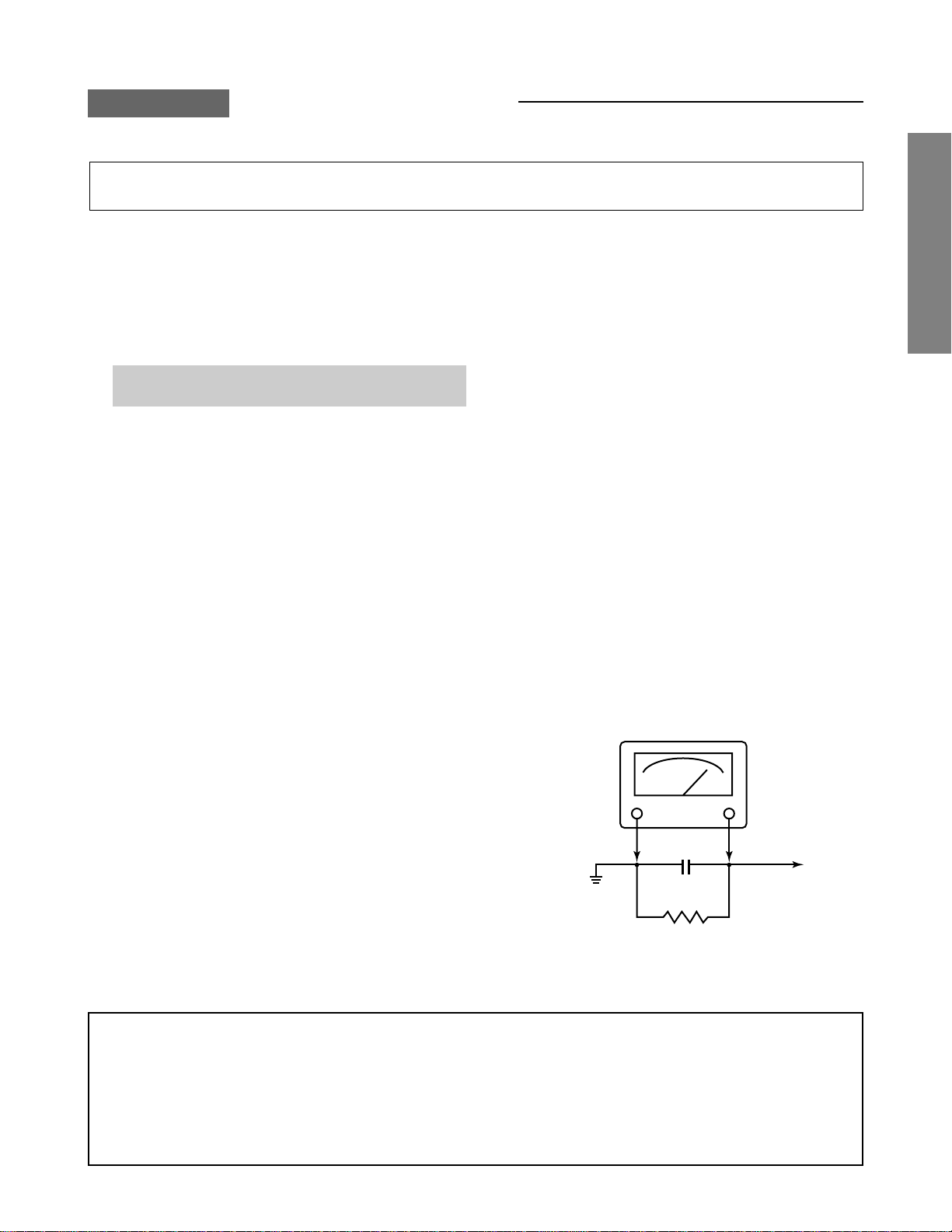
AC VOLTMETER
0.15µF
Good earth ground
such as a water
pipe, conduit, etc.
Place this probe on
each exposed
metallic part.
1500 ohm
10 watt
SAFETY INSTRUCTIONS
WARNING: BEFORE SERVICING THIS CHASSIS, READ THE “X-RAY RADIATION PRECAUTION”, “SAFETY PRECAU-
TION” AND “PRODUCT SAFETY NOTICE” INSTRUCTIONS BELOW.
X-RAY RADIATION PRECAUTION
1. Excessive high voltage can produce potentially hazardous
X-RAY RADIATION. To avoid such hazards, the high voltage must not be above the specified limit. The nominal
value of the high voltage of this receiver is (A) kV at zero
beam current (minimum brightness) under a 120V AC
power source. The high voltage must not, under any circumstances, exceed (B) kV.
Refer to table-1 for high voltage (A), (B).
(See SETTING & ADJUSTING DATA on page 12)
Each time a receiver requires servicing, the high voltage
should be checked following the HIGH VOLTAGE CHECK
procedure in this manual. It is recommended that the reading of the high voltage be recorded as a part of the service
record. It is important to use an accurate and reliable high
voltage meter.
SAFETY PRECAUTION
2. This receiver is equipped with a Fail Safe (FS) circuit which
prevents the receiver from producing an excessively high
voltage even if the B+ voltage increases abnormally. Each
time the receiver is serviced, the FS circuit must be checked
to determine that the circuit is properly functioning, following the FS CIRCUIT CHECK procedure in this manual.
3. The only source of X-RAY RADIATION in this TV receiver
is the picture tube. For continued X-RAY RADIATION protection, the replacement tube must be exactly the same
type tube as specified in the parts list.
4. Some part in this receiver have special safety-related characteristics for X-RAY RADIATION protection. For continued safety, parts replacement should be undertaken only
after referring to the PRODUCT SAFETY NOTICE below.
GENERAL ADJUSTMENTS
WARNING : Service should not be attempted by anyone unfamiliar with the necessary precautions on this receiver. The following are the necessary precautions to be observed before
servicing this chassis.
1. An isolation Transformer should be connected in the power
line between the receiver and the AC line before any service is performed on the receiver.
2. Always discharge the picture tube anode to the CRT conductive coating before handling the picture tube. The picture tube is highly evacuated and if broken, glass fragments will be violently expelled. Use shatter proof goggles and keep picture tube away from the unprotected body
while handling.
3. When replacing a chassis in the cabinet, always be certain that all the protective devices are put back in place,
such as; non-metallic control knobs, insulating covers,
shields, isolation resistor-capacitor network etc.
4. Before returning the set to the customer, always perform
an AC leakage current check on the exposed metallic parts
of the cabinet, such as antennas, terminals, screwheads,
metal overlays, control shafts etc. to be sure the set is
safe to operate without danger of electrical shock. Plug
the AC line cord directly into a 120V AC outlet (do not use
a line isolation transformer during this check). Use an AC
voltmeter having 5000 ohms per volt or more sensitivity in
the following manner:
Connect a 1500 ohm 10 watt resistor, paralleled by a 0.15
µF, AC type capacitor, between a known good earth ground
(water pipe, conduit, etc.) and the exposed metallic parts,
one at a time. Measure the AC voltage across the combination of 1500 ohm resistor and 0.15 µF capacitor. Reverse the AC plug at the AC outlet and repeat AC voltage
measurements for each exposed metallic part. Voltage
measured must not exceed 0.3 volts rms. This corresponds
to 0.2 milliamp. AC. Any value exceeding this limit constitutes a potential shock hazard and must be corrected immediately.
Many electrical and mechanical parts in this chassis have special safety-related characteristics. These characteristics are
often passed unnoticed by a visual inspection and the protection afforded by them cannot necessarily be obtained by using
replacement components rated for higher voltage, wattage, etc. Replacement parts which have these special safety characteristics are identified in this manual and its supplements; electrical components having such features are identified by the
international hazard symbols on the schematic diagram and the parts list.
Before replacing any of these components, read the parts list in this manual carefully. The use of substitute replacement
parts which do not have the same safety characteristics as specified in the parts list may create shock, fire, X-ray radiation
or other hazards.
PRODUCT SAFETY NOTICE
– 3 –
WARNING: BEFORE SERVICING THIS CHASSIS, READ THE “X-RAY RADIATION PRECAUTION”, “SAFETY PRECAU-
TION” AND “PRODUCT SAFETY NOTICE” ON PAGE 3 OF SERVICE MANUAL.
■ The following adjustments should be made when a complete realignment is required or a new picture tube is installed.
Perform the adjustments in order as follows :
1. Color Purity
2. Convergence
3. White Balance
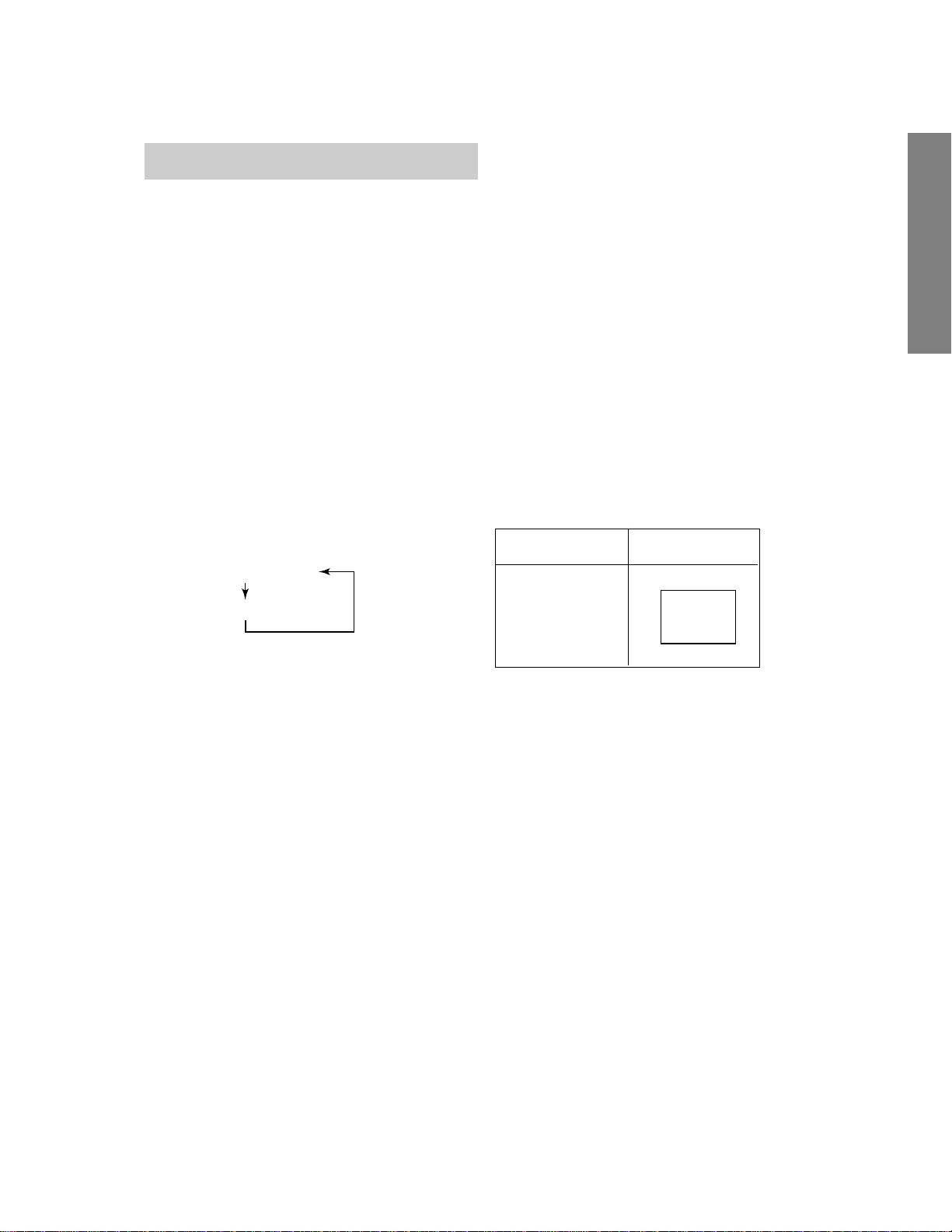
Note: The PURITY/CONVERGENCE MAGNET assembly and rubber wedges need mechanical positioning.
Refer to figure 1.
COLOR PURITY ADUSTMENT
GENERAL ADJUSTMENTS
(1)Let the screen face in the installing direction or toward the east (when it is to be moved), bring up the service mode
screen after demagnetizing (front, left, right, and top) with the degaussing coil, receive white signals by pressing the
[TV/VIDEO] button, and then the receiver should be operated for more than 40 minutes.
(2)Perform rough adjustment of the central convergence with the P/C magnet according to the adjustment item.
(3)Receive built-in green signals, loosen set screws on the deflection yoke, remove rubber wedges, and shift the deflection
yoke to toward front.
(4)Move alternately the two 2-pole magnets of the P/C magnets so that the green raster can come to the center of the
screen.
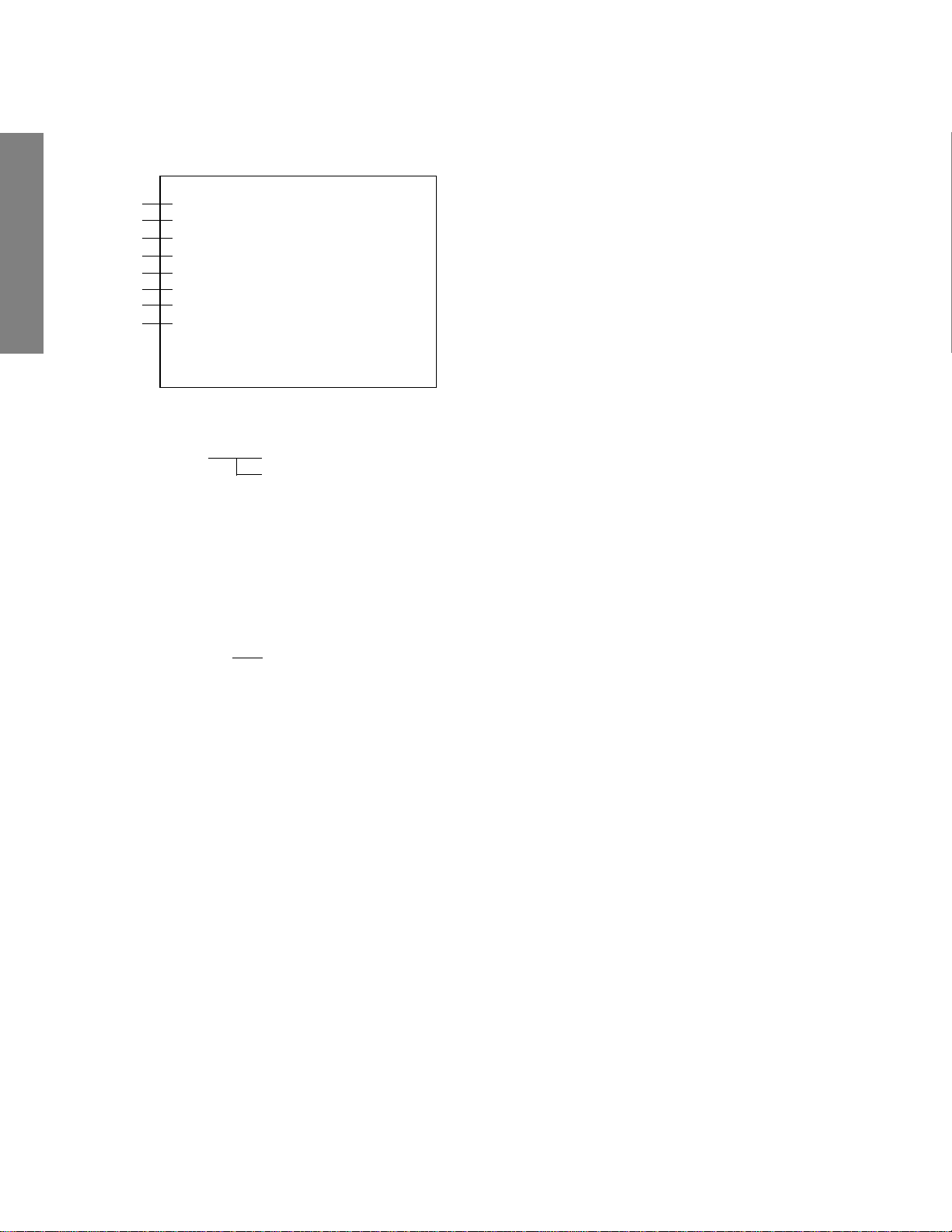
SET-UP ADJUSTMENT FOR FLAT TUBE
Figure 1.
2-pole purity magnet
(27": Magnet is fixed with deflection yoke.)
Green Belt
Sub-4-pole convergence magnet (32" : 34")
Sub-4-pole convergence magnet (to be installed on deflection yoke for 30", 32”)
Main 4-pole convergence magnet (30" : 32")
6-pole convergence magnet (34")
6-pole convergence magnet (30" : 32")
Main 4-pole convergence magnet (34")
P/C magnet installing position A
• 30"=26.5 mm
A
• 32"=30.5 mm or 32.5 mm
• 34"=37 mm
• 34"=39 mm
(5)Receive built-in red and blue signals, check that there is no inclination of the single color raster toward one side, and if
each color tilts to a great extent, make adjustment with the 2-pole magnet so that the 3 colors will come to the center
evenly.
(6)Receive the green raster, shift the deflection yoke from a
foremost position (hitting against the picture tube) to a
Shift deflection yoke
(7) Perform marking of each point on
(6)
(8)
the tape of picture tube
backward position horizontally, stop the deflection yoke
at a position where it begins to become a green raster,
and perform accurate marking on the picture tube.
(7)Shift the deflection yoke further backward, and perform
Picture tube
CRT-D board
accurate marking at a position where the green raster
begins to being luck.
(8)Fix the deflection yoke at a position 60% forward within
the range marked in items (6) and (7) above.
CONVERGENCE ADJUSTMENTS
100 60 0%
Fix the deflection yoke at a position 60% forward from a point
between (6) and (7)
P/C Mag
* Adjust the convergence magnet to get vest convergence in the the order to (1) ~ (5).
■ CENTER CONVERGENCE:
(1)Receive the white crosshatch or dot pattern from the service signal generator.
(2)Use the 2 pieces of main 4-pole magnets of P/C magnets, change the open angle, and align the red and blue vertical
lines on the screen center.
(3)Freeze the open angle of the main 4-pole magnets, turn them simultaneously, and align the horizontal lines.
(4)Take the same steps for items (2) and (3) above and align red/blue with green on the screen center using two 6-pole
magnets.
– 4 –
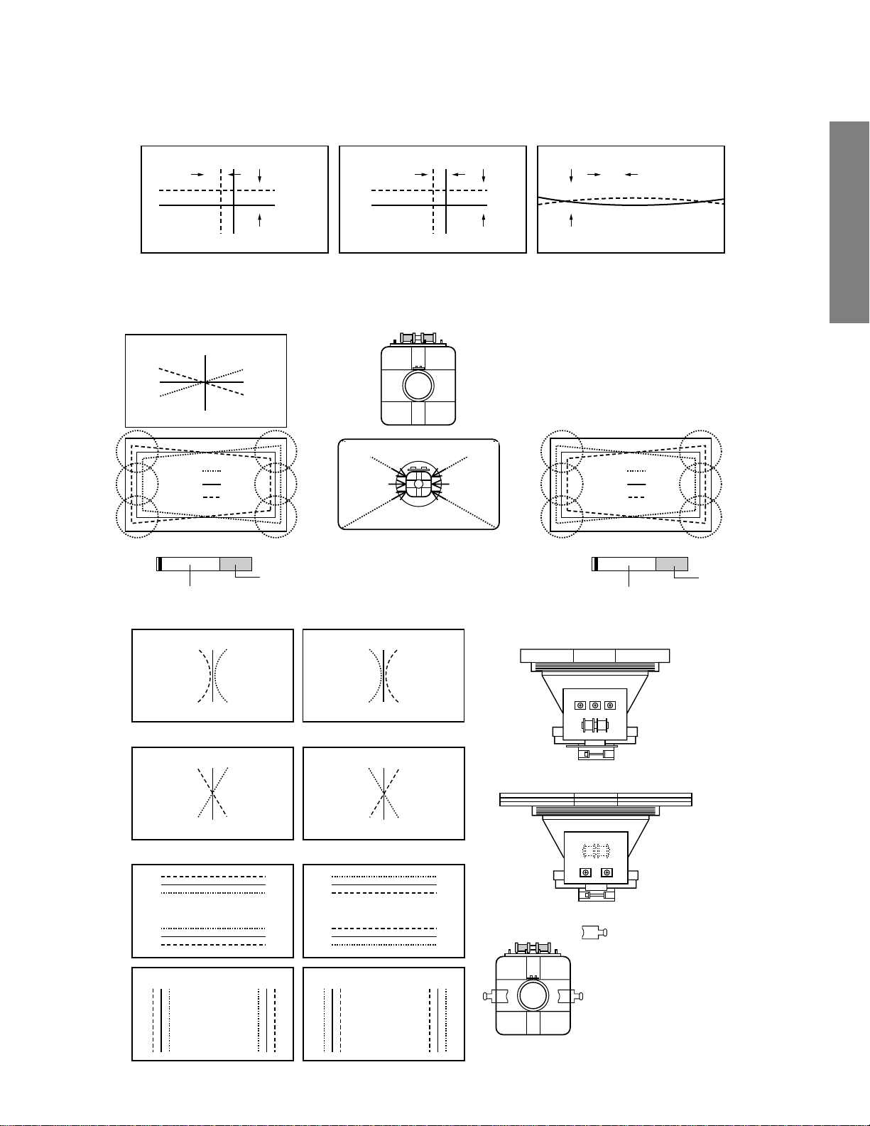
(5)Adjust the sub-4-pole magnets only in case there is any deviation of Xv bow-shaped convergence. (To be usually set at
the initial position)
Align both sides with the sub-4-pole magnets and minimize the deviation of blue and red with the main 4-pole magnets.
blue
blue
red
red
Main 4-pole magnet
red/blue
red/blue
green
6-pole magnet
■ CIRCUMFERENCE CONVERGENCE:
Perform correction in the following manner.
*
blue
green
red
A
B
C
(Parts code:23 948 274) TC-S
blue
green
red
S
N
Blue color or blue mark
D
E
F
*Insert the correction piece between the
picture tube and the deflection yoke.
Bonded surface
(Insertion position of correction
piece)
D
E
F
A
B
C
Adjust VR 1 and minimize the deviation of YH. *Only 27", 30" and 32".
Red
green
blue
blue
green
Red
Xv bow-shaped deviation of convergence
blue
green
red
Sub-4-pole magnet
• Adjust coils and minimize deviation
(The 27” unit has coils underneath it)
A
B
C
■ 30", 27", 32"
blue
green
red
(Parts code:23 948 464)
N
S
Transparent
GENERAL ADJUSTMENTS
D
E
F
Bonded surface
Red
green
blue
blue
green
Red
Adjust VR 2 (YHC) and minimize the deviation of YH.
Red
blue
green
green
blue
Red
blue
Red
green
green
Red
blue
Adjust VR 3 (YV) and minimize the deviation of YV.
Red
green
blue
blue
green
Red
GH
Red
blue
green
green
blue
red
green
blue
red
green
green
Red
– 5 –
blue
Red
Red
blue
blue
green
VR3
VR2 VR1
■ 34"
YV YHC
27" (Part No. 23 947 371)
32", 30" (Part No. 23 947 121)
34" (Part No. 23 993 080)
GH
Perform correction by inserting the
correction piece into the clearance of terminal board coils of
the deflection yoke.
Note:
Perform insertion by turning the
metal side to the terminal board
side of the deflection yoke.
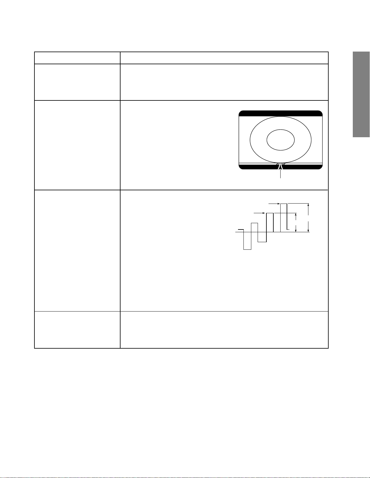
1. ENTERING TO SERVICE MODE
1) Press MUTE button twice
on Remote Control.
SERVICE MODE
2) Press MUTE button
again to keep pressing.
3) While pressing the MUTE button,
press MENU button on TV set.
S
1/2 MUTE
GENERAL ADJUSTMENTS
2. DISPLAYING THE ADJUSTMENT MENU
1) Press MENU button on TV.
Service mode
3. KEY FUNCTION IN THE SERVICE MODE
The following key entry during display of adjustment menu provides special functions.
A single horizontal line ON/OFF: TV (ANT)/VIDEO button (on TV)
Test signal selection : TV (ANT)/VIDEO button (on Remote)
Selection of the adjustment items : Channel s/t (on TV or Remote)
Change of the data value : Volume s/t (on TV or Remote)
Adjustment menu mode ON/OFF : MENU button (on TV)
Initialization of the memory (QA02, QA04) : RECALL+Channel (s) button on TV
Initialization of the self diagnostic data: RECALL+Channel (t) button on TV
“RCUT” selection : 1 button
“GCUT” selection : 2 button
“BCUT” selection : 3 button
“CNTX” selection : 4 button
“COLC” selection : 5 button
“TNTC” selection : 6 button
Test audio signal ON/OFF (1kHz) : 8 button
Self diagnostic display ON/OFF : 9 button
MUTE
(Service mode display)
Adjustment mode
S
Press
Press
Item
Data
– 6 –
4. SELECTING THE ADJUSTING ITEMS
1) Every pressing of CHANNEL s button in the service mode changes the adjustment items in the order of table-2.
(t button for reverse order)
Refer to table-2 for preset data of adjustment mode.
(See SETTING & ADJUSTING DATA on page 12)
5. ADJUSTING THE DATA
1) Pressing of VOLUME s or t button will cahnge the value of data in the range from 00H to FFH. The variable range
depends on the adjusting item.
6. EXIT FROM SERVICE MODE
1) Pressing POWER button to turn off the TV once.
■ INITIALIZATION OF MEMORY DATA OF QA02 AND QA04
After replacing QA02 and QA04, the following initialization is required.
1. Enter the service mode, then select any register item.
2. Press and hold the RECALL button on the Remote, then press the CHANNEL s button on the TV. The initialization of QA02
and QA04 has been complated.
3. Check the picture carefully. If necessary, adjust any adjustment item above.
Perform “Programming Channel Memory” on the owner's manual.
CAUTION: Never attempt to initialize the data unless QA02, QA04 has been replaced.
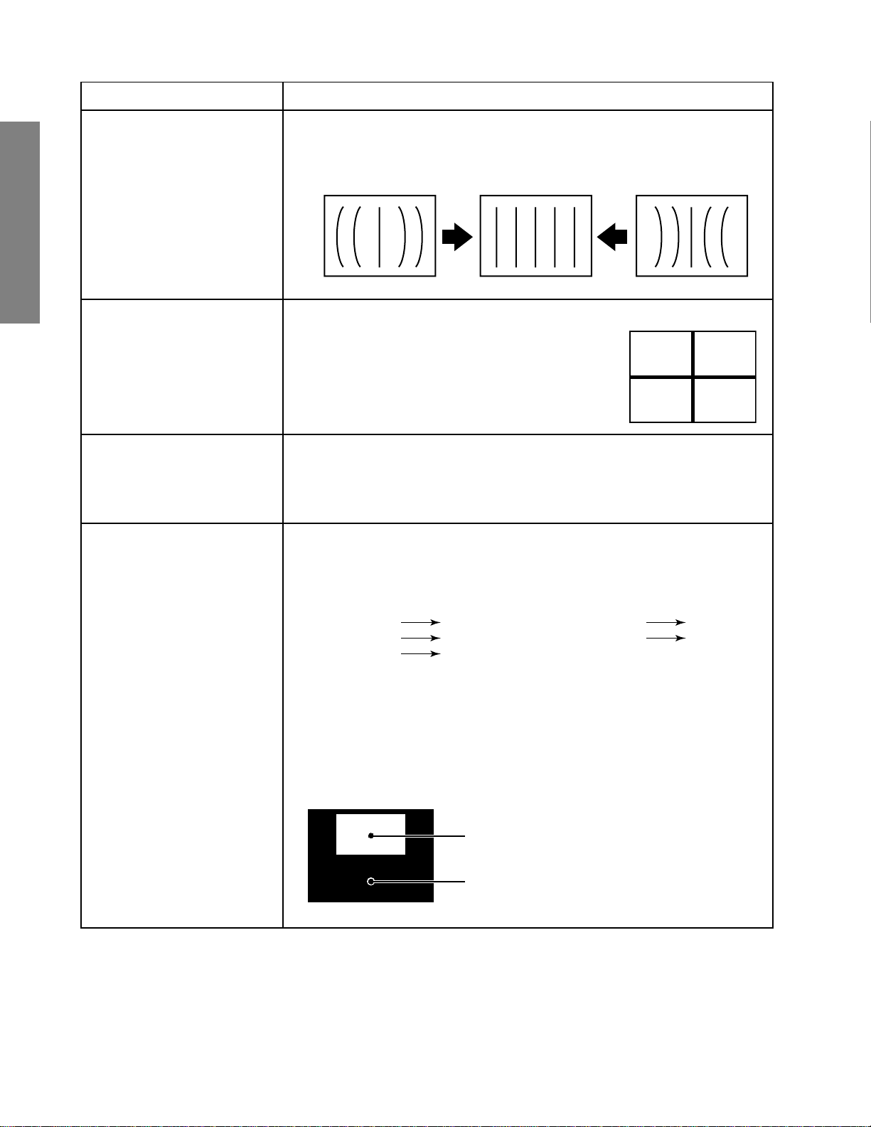
7. TEST SIGNAL SELECTION
1) Every pressing of TV/VIDEO button on the Remote Control in the Service mode changes the built-in test patterns
on screen in the following order.
GENERAL ADJUSTMENTS
Signals Picture
Normal picture
All white
2) Press “8” button while any built-in test pattern to on the screen to output the 1 kHz sound. Press the button again to
cut off the sound.
Note: If the video cable is connected to the VIDEO1 INPUT jack, the built-in pattern signals are not displayed.
• All White
– 7 –
8. SELF DIAGNOSTIC FUNCTION
1) Press “9” button on Remote Control during display of adjustment menu in the service mode.
The diagnosis will begin to check if interface among IC’s are executed properly.
2) During diagnosis, the following displays are shown.
SELF CHECK
GENERAL ADJUSTMENTS
Part number of microprocessor (QA01)
Operation number of protection circuit (current limiter) . . . . “000” is normal.
BUS line check “OK” ................... Normal
BUS line ACK (acknowledge) check
Sync. signal check Green display ..... Normal
ID code for TV set
Version of "EEP"
Data for "OPT"
NO. 23 * * * * * *
POWER : 000
BUS LINE : OK
BUS CONT : OK
BLOCK : MAIN SUB
SET ID : FF
EEP VER : FF
OPT1 : 02 OPT2 : A4
DVI
NO 23009621
ERR CODE : 030000
“SCL-GND” or “NG” .......... SCL-GND short circuit
“SDA-GND” or “NG” .......... SDA-GND short circuit
“SCL-SDA” or “NG” ........... SCL-SDA short circuit
“OK” ..................... Normal
Display of Location Number . . . . NG
(Display example)
“QA02 NG”, “H001 NG”, “Q501 NG” etc.
Note: The indication of failure place is only one place though failure places are plural. When
repair of a failure place finishes, the next failure place is indicated. (The order of priority of
indication is left side.)
Cyan display ...... No check
Red display ........ NG
MAIN....... Main sync
SUB ........ Sub sync (when turn on the PIP)
– 8 –
ELECTRICAL ADJUSTMENTS
ITEM ADJUSTMENT PROCEDURE
FOCUS VR ADJ
SUB-BRIGHTNESS
(BRTC)
SUB-COLOR
(SCOL)
SUB-TINT
(TNTC)
1. Enter the service mode, then select any register item.
2. Press the TV/VIDEO button on the Remote until the black cross-bar pattern appears on the screen.
3. Adjust the FOCUS control (on T461) for well defined scanning lines on the picture
screen.
1. Constrict the picture height until the vertical retrace line appears adjusting the item
HIT (HEIGHT).
2. Adjust the CONTRAST control to the minimum.
3. Call up the adjustment mode display, then
select the item BRTC.
4. Press the VOLUME s or t button so the
belt of vertical retrace line just disappear.
5. Adjust the CONTRAST control for the desired contrast.
6. Perform the HEIGHT adjustment.
Vertical retrace line
1. Receive color-bar signal from color-bar
generator.
2. Press the RESET button.
3. Connect oscilloscope to TP501 on SIGNAL board.
4. Adjust the CONTRAST control to the
minimum.
Magenta
0
Blue
2
3 (1.6V
5. Call up the adjustment mode display,
then select the item TNTC.
6. Adjust the SUB-TINT by pressing the
VOLUME s or t button to obtain a blue
bar to magenta bar ratio of 3:2 as shown.
7. Press the RESET button.
8. Select the item SCOL.
9. Adjust the SUB-COLOR by pressing the VOLUME s or t button to achieve
1.6V0-p of a blue bar on scope.
10. Check the picture with off-air signal.
0-P
GENERAL ADJUSTMENTS
)
WIDTH
(WID)
1. Call up the adjustment mode display, then select the item WID.
2. Press the VOLUME s or t button to get the picture so the left and right edges of
raster begins to lack.
3. Press the VOLUME s or t button to advance the data by 7 steps.
Note : Check the horizontal picture position is correct.
– 9 –
ITEM ADJUSTMENT PROCEDURE
E-W PARABOLA (DPC)
(PARA)
GENERAL ADJUSTMENTS
HORIZONTAL POSITION
(HPOS)
VERTICAL POSITION
(VPOS)
HEIGHT
(HIT)
1. Call up the adjustment mode display, then select the item PARA.
2. Press the TV/VIDEO button on Remote until the cross-hatch pattern appears on
the screen.
3. Press the VOLUME s or t button to make vertical lines straight as shown below.
1. Call up the adjustment mode display, then select the item HPOS or VPOS.
2. Press the TV/VIDEO button on Remote until the
white cross-bar or black cross-bar pattern appears
on the screen.
3. Adjust the HORIZONTAL and VERTICAL position
alternately by pressing the VOLUME s or t button for proper picture position.
4. Check the picture with off-air signal.
1. Call up the adjustment mode display, then select the item HIT.
2. Press the VOLUME s or t button to get the picture so the top of raster begins to
lack.
3. Press the VOLUME s button to advance the data by 9 steps.
Note : Check the vertical picture position is correct.
WHITE BALANCE
(RCUT)
(GCUT)
(BCUT)
(GDRV)
(BDRV)
1. Adjust the CONTRAST control to the center, and BRIGHTNESS control to the
maximum.
2. Call up the adjustment mode display, and press the TV/VIDEO button on Remote
until the white and black pattern appears on the screen.
3. Adjust the following items with the CHANNEL s/t and VOLUME s/t buttons.
RCUT
Item :
GCUT
Item :
BCUT
Item :
4. Press the TV/VIDEO button on TV to display a single horizontal line on the screen.
5. Turn the SCREEN control (FBT) fully counterclockwise and gradually rotate clockwise until the first horizontal line appears slightly on the screen.
6. Press the TV/VIDEO button to display the normal picture.
7. Adjust the remaining two “?CUT” items (CHANNEL s/t → TV/VIDEO → VOL-
UME s/t in order) to obtain the slightly lighted horizontal line in the same levels of
three (red, green, blue) colors. The line should be white if the adjustments are
proper.
Data : 40H
Data : 40H
Data : 40H
Bright area
Adjust "GDRV" or "BDRV" to be white.
Dark area
Fine adjust "RCUT", "GCUT" or "BCUT" to be black.
Item :
GDRV Data : 40H
Item :
BDRV Data : 40H
– 10 –
CIRCUIT CHECKS
HIGH VOLTAGE CHECK
CAUTION: There is no HIGH VOLTAGE ADJUSTMENT on
this chassis. Checking should be done following the steps
below.
1. Connect an accurate high voltage meter to the second anode of the picture tube.
2. Turn on the receiver. Set the BRIGHTNESS and CONTRAST controls to minimum (zero beam current).
3. High voltage must be measured below (B) kV.
Refer to table-1 for high voltage (B).
(See SETTING & ADJUSTING DATA on page 12)
4. Vary the BRIGHTNESS control to both extremes to be sure
the high voltage does not exceed the limit under any conditions.
FS CIRCUIT CHECK
The Fail Safe (FS) circuit check is indispensable for the final
check in servicing. Checking should be done following the
steps below.
1. Turn the receiver on and press the RESET button.
2. Temporarily short TP-(R) and TP-(X) with a jumper wire.
Raster and sound will disappear.
3. The receiver must remain in this state even after removing
the jumper wire. This is the evidence that the FS circuit is
functioning properly.
4. To obtain a picture again, temporarily turn the receiver off
and allow the FS circuit more than 5 seconds to reset. Then
turn the power switch on to produce a normal picture.
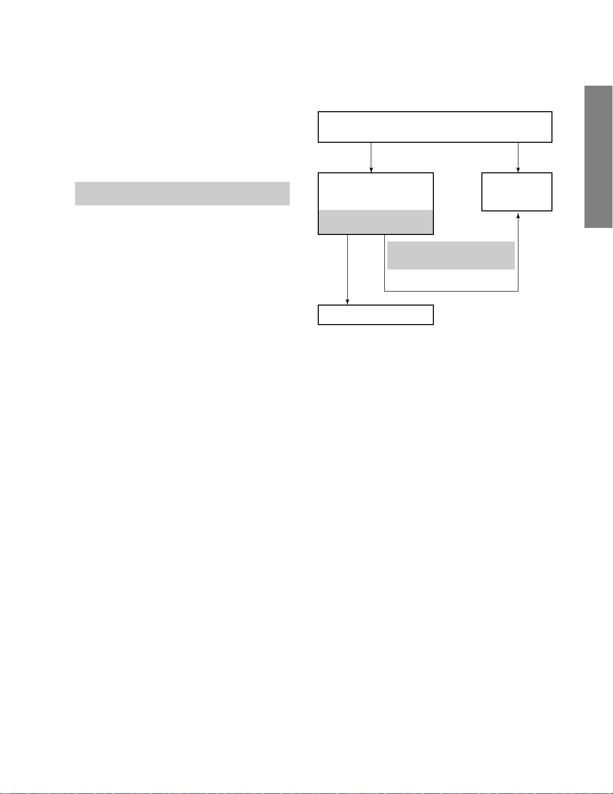
Troubleshooting Guide for Fail Safe Circuit
Check that the set returns to normal operation when pin 12
of Z801(or emitter of Q472) is grounded with jumper wire.
YES NO
Check the voltage across
Capacitor C471 is
approximately
Refer to table –3 for
FBT detection voltage
YES
Defective Fail Safe Circuit
(C)
volts.
(C)
(See SETTING & ADJUSTING
DATA on page 12)
.
NO
Faulty power
circuit or horizontal circuit.
GENERAL ADJUSTMENTS
– 11 –
CHAPTER 2 SPECIFIC INFORMATIONS
SAFETY INSTRUCTIONS
SERVICE MODE
GENERAL ADJUSTMENTS
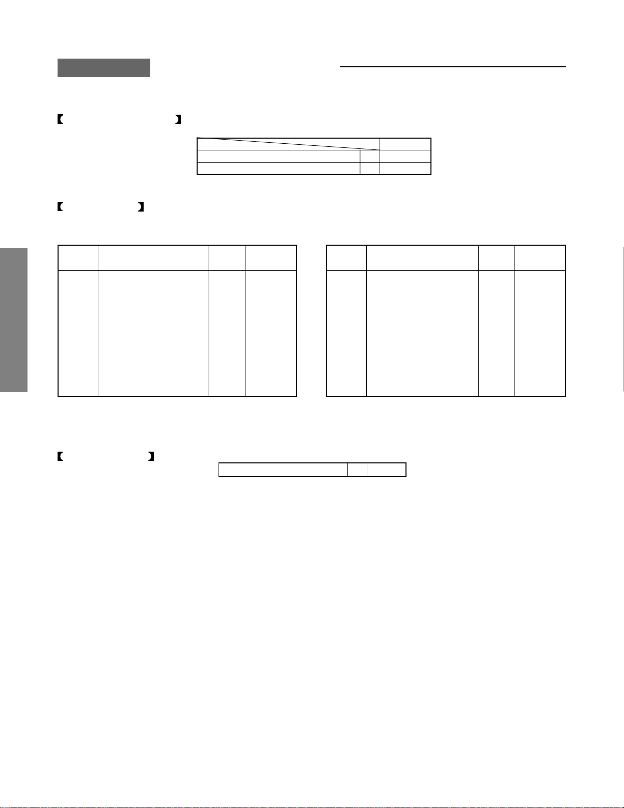
ADJUSTING ITEMS AND DATA IN THE SERVICE MODE:
SETTING & ADJUSTING DATA
34"
HIGH VOLTAGE AT ZERO BEAM: (A) 30.0 kV
MAX HIGH VOLTAGE:
Table-1
(B) 35.0 kV
Item Name of adjustment
RCUT
GCUT
BCUT
GDRV
BDRV
BRTC
TNTC
SPECIFIC INFORMATIONS
SCNT
HIT
CIRCUIT CHECKS
R CUT OFF
G CUT OFF
B CUT OFF
G DRIVE
B DRIVE
BRIGHT CENTER
TINT CENTTER
SUB CONTRAST
PICTURE HIT
(Basis)
(Basis)
(Basis)
(Basis 1,4,7,10)
(Basis 1,4,7,10)
(1-12)
(1,2,3)
(1,2,3)
(1080)
Preset
40H
40H
40H
40H
40H
80H
46H
15H
38H
NORMAL
& FULL
←
←
←
←
←
←
←
12H
24H
Table-2
FBT DETECTION VOLTAGE (C) 20.1 V
Table-3
Item Name of adjustment Preset
LIN
WID
PARA
CNR
TRAP
HPS
TCNR
BCNR
VPSI
V-LINEARITY
PICTURE WIDTH
E-W PARABOLA
EW M CORRECTION
EW TRAPEZIUM
H-POSITION
EW TOP CORNER
EW BOTTOM COR
VTRAP (VPS1)
(1080)
(1080)
(1080)
(1080)
(1080)
(1080)
12H
00H
16H
15H
35H
39H
14H
10H
82H
NORMAL
& FULL
←
20H
←
←
←
46H
←
←
6DH
– 12 –

TV Front
LOCATION OF CONTROLS
Remote sensor
MENU ; : ts
TV/VIDEO
CHANNELVOLUMEMENU
S-VIDEO
L/MONO
VIDEO-3 IN
Power indicator
R
AUDIOVIDEO
POWER
GENERAL ADJUSTMENTS
TV Rear
Video 3
Video/Audio inputs
(behind the door)
ANT OUT
VIDEO
MONO
AUDIO
ANT( 75
COLOR
STREAM HD-1
Y
PB
PR
L/
L
AUDIO
R
R
IN
ANT-2 IN
)
ANT-1 IN
ANT-1 ANT-2OUT
VIDEO 1
S-VIDEO
VIDEO
L/
MONO
AUDIO
R
VIDEO 2
S-VIDEO
MENU
COLOR
STREAM HD-2
Y
PB
PR
L
AUDIO
R
VIDEO
L/
MONO
AUDIO
R
R
AUDIO
OUT
Volume ; :
DV/HDCP IN
DVI/HDCP IN
L
L
VAR
AUDIO
ON OFF
R
Channel tsTV/VIDEO
AUDIO CENTER
CHANNEL IN
POWER
SPECIFIC INFORMATIONS
VIDEO 1/2
ColorStream
HD-1
Video/
Audio OUT
ColorStream
HD-2
– 13 –
Audio Center Channel IN
Variable Audio OUT
Remote Control
GENERAL ADJUSTMENTS
TOP MENU (DVD only)
SPECIFIC INFORMATIONS
+10 (DVD only)
ENTER
Device Switch
PAUSE
TV/VCR (VCR only)
REW
TV / VIDEO
RECALL
INFO
123
456
7
100
N
E
M
P
O
T
FAVORITE
E
N
T
E
E
R
N
T
E
R
TV
CBL/SAT
VCR
DVD
TV/VCR PAUSE
CH SCAN
REC
89
+10
0
U
FAV
MENU
DVDMENU
FAV
VOLCH
POP DIRECT CH MUTE SLEEP
STOP
FREEZE SOURCE
FFREW
SKIP / SEARCH
SWAP POP CH
POWER
CHRTN
ENT
G
PIC SIZE
E
PLAY
SPLIT
LIGHT
POWER
INFO (CBL/SAT only)
Channel Numbers (0-9)
U
I
D
E
GUIDE (CBL/SAT only)
89; : (DVD only)
IT
X
R
A
E
L
C
CLEAR (DVD only)
CH 89
PLAY
STOP
SKIP/SEARCH
(DVD only)
REC (VCR only)
FF
– 14 –
SKIP/SEARCH
(DVD only)

ADDING CHANNELS TO THE TV’S MEMORY
When you press Channel 8 or 9, your TV will stop only on the channels stored in the TV’s channel memory.
Follow the steps below to program all active channels into the TV’s memory.
Programming channels automatically
Your TV can automatically detect all active channels in your
area and store them in its memory. After the channels are
stored automatically, you can manually add or erase
individual channels (see “Adding and erasing channels
manually,” below).
To program channels automatically:
Press MENU, and then press ; or : until the SET UP
1
menu appears.
Press 8 or 9 until the TV/CABLE is highlighted.
2
Press ; or : to highlight either TV or CABLE, depend-
3
ing on which you use. If you use an antenna, highlight
TV; if you use cable, highlight CABLE.
Press 9 to select CH PROGRAM.
4
Press ; or : to start channel programming. The TV will
5
automatically cycle through all the TV or Cable channels
(depending on which you selected), and store all active
channels in the channel memory.
While the TV is cycling through the channels, the
message “Programming Now—Please Wait” appears.
When channel programming is complete, the message
6
“Completed” appears.
Press Channel 8 or 9 to view the programmed chan-
7
nels.
Adding and erasing channels manually
After you have programmed the channels automatically, you
can manually add or erase specific channels.
To add or erase channels:
Select the channel you want to add or erase. If you are
1
adding a channel, you must select the channel using the
Channel Number buttons.
Press 8 or 9 to highlight ADD/ERASE.
3
Press ; or : to select ADD or ERASE, depending on
4
the function you want to perform.
Repeat steps 1-4 for other channels you want to add or
5
erase.
Using the Quick Connect Guide
The Quick Connect Guide automatically starts the first time
the TV is turned on.
You can change the current settings any time.
Press MENU, and then press ; or : until the SET UP
1
menu appears.
Press 8 or 9 to highlight “QUICK CONNECT GUIDE”.
2
Press ; or : to enter the Quick Connection Guide
3
mode.
Advance the setup according to the guide displayed on
the screen.
You can set up the following items.
On-screen display language selection
Ye s
Cable box connection
Cable box output channel selection
(ch3/ch4)
Select channels using Cable box
(Confirmation only)
Cable box selection (Yes/No)
Cable or Antenna connection
TV (antenna)/Cable source selection
Automatic channel programming
Clock setting
Picture mode selection
Basic setup has been completed
GENERAL ADJUSTMENTS
SPECIFIC INFORMATIONS
No
Press MENU, and then press ; or : until the SET UP
2
menu appears.
– 15 –

CHASSIS AND CABINET REPLACEMENT PARTS LIST
WARNING: BEFORE SERVICING THIS CHASSIS, READ THE “X-RAY RADIATION PRECAUTION”, “SAFETY
PRECAUTION” AND “PRODUCT SAFETY NOTICE” ON PAGE 3 OF THIS MANUAL.
CAUTION: The international hazard symbols “ ” in the schematic diagram and the parts list designate components
which have special characteristics important for safety and should be replaced only with types identical to those in the
original circuit or specified in the parts list. The mounting position of replacements is to be identical with originals.
Before replacing any of these components, read carefully the PRODUCT SAFETY NOTICE. Do not degrade the
safety of the receiver through improper servicing.
NOTICE:
•
The part number must be used when ordering parts, in order to assist in processing, be sure to include the Model
number and Description.
•
The PC board assembly with * mark is no longer available after the end of the production.
Model : 34HX83
Capacitors ............. CD : Ceramic Disk PF : Plastic Film EL : Electrolytic
Resistors ............... CF : Carbon Film CC : Carbon Composition MF : Metal Film
OMF : Oxide Metal Film VR : Variable Resistor FR : Fusible Resistor
(All CD and PF capacitors are ±5%, 50V and all resistors, ±5%, 1/6W unless otherwise noted.)
Location
Parts No. Description
No.
CAPACITORS
C101 24796339 ELECTROLYTIC CE04G 35V 3.3UF M
C102 24665221 ELECTROLYTIC, 10V 220UF M 3A
SPECIFIC INFORMATIONS
C105 24100102 CERAMIC CHIP, 50V F 1000PF Z
C106 24669479 ELECTROLYTIC, 50V 4.7UF M 3A
C107 24666221 ELECTROLYTIC, 16V 220UF M 3A
C112 24665221 ELECTROLYTIC, 10V 220UF M 3A
C115 24100102 CERAMIC CHIP, 50V F 1000PF Z
C117 24666221 ELECTROLYTIC, 16V 220UF M 3A
C118 24665221 ELECTROLYTIC, 10V 220UF M 3A
C198 24100104 CERAMIC CHIP, 25V F 0.1UF Z
C201 24109103 CERAMIC CHIP, 50V B 0.01UF K
C205 24766229 ELECTROLYTIC, 50V 2.2UF M
C206 24794220 ELECTROLYTIC, 16V 22UF M
C307 24693823 PLASTIC FILM CQ921 M 100V 0.082MF J
C308 24668221 ELECTROLYTIC, 35V 220UF M 3A
C309 24212101 CERAMIC DISC, 50V B 100PF K
C310 24667102 ELECTROLYTIC, 25V 1000UF M 3A
C311 24214152 CERAMIC DISC, 500V B 1500PF K
C313 24082057 PLASTIC FILM, 100V 0.22UF J
C314 24591563 PLASTIC FILM, 50V 0.056UF J
C320 24667221 ELECTROLYTIC, 25V 220UF M 3A
C322 24539105 PLASTIC FILM, 50V 1UF J
C323 24539105 PLASTIC FILM, 50V 1UF J
C325 24591203 PLASTIC FILM, 50V 0.02UF J
C326 24669010 ELECTROLYTIC, 50V 1UF M 3A
C327 24073041 ELECTROLYTIC, 16V 470UF M 3A
C331 24667102 ELECTROLYTIC, 25V 1000UF M 3A
C332 24591562 PLASTIC FILM, 50V 5600PF J
C333 24109332 CERAMIC CHIP, 50V B 3300PF K
C362 24591123 PLASTIC FILM, 50V 0.012MF J
C370 24666100 ELECTROLYTIC, 10V 10UF M 3A
C402 24092463 CERAMIC CHIP, 16V B 0.22UF K
C404 24669229 ELECTROLYTIC, 50V 2.2UF M 3A
C406 24109223 CERAMIC CHIP, 25V B 0.022UF K
C410 24109221 CERAMIC CHIP, 50V B 220PF K
C413 24214392 CERAMIC DISC, 500V B 3900PF K
C416 24676330 ELECTROLYTIC, 100V 33UF M 3A
C417 24214391 CERAMIC DISC, 500V B 390PF K
Location
* C428 24503192 PLASTIC FILM, 400V 0.15UF J
* C442 24503190 PLASTIC FILM, 400V 0.12UF J
* C443 24503348 PLASTIC FILM, 1800VH 3900PF H
* C444 24503196 PLASTIC FILM CF92 T 1800VH 5600PF H
* C461 24820123 PLASTIC FILM, 630V 0.012UF J
* C467 24820123 PLASTIC FILM, 630V 0.012UF J
Parts No. Description
No.
C418 24667221 ELECTROLYTIC, 25V 220UF M 3A
C432 24763101 ELECTROLYTIC, 16V 100UF M
C439 24503459 PLASTIC FILM, 400V 0.068UF J
C445 24095804 PLASTIC FILM, 400V 0.056UF J
C446 24073120 ELECTRPLYTIC, 250V 33UF, 250YXF33M
C448 24073118 ELECTROLYTIC, 160V 33UF M
C450 24092341 CERAMIC DISC, 2KV R 470PF K
C451 24092341 CERAMIC DISC, 2KV R 470PF K
C452 24820103 PLASTIC FILM, 630V 0.01UF J
C464 24503149 PLASTIC FILM, 250V 3.3UF
C465 24591183 PLASTIC FILM, 50V 0.018UF J
C466 24679220 ELECTROLYTIC, 250V 22UF M 3A
C468 24591823 PLASTIC FILM, 50V 0.082UF J
C469 24591122 PLASTIC FILM, 50V 1200PF J
C470 24766220 ELECTROLYTIC, 50V 22UF M
C471 24766479 ELECTROLYTIC, 50V 4.7UF M
C472 24539104 PLASTIC FILM, 50V 0.1UF J
C476 24214471 CERAMIC DISC, 500V B 470PF K
C477 24666220 ELECTROLYTIC, 16V 22UF M 3A
C482 24109122 CERAMIC CHIP, 50V B 1200PF K
C488 24666100 ELECTROLYTIC, 10V 10UF M 3A
C502 24092730 CERAMIC CHIP, 16V B 0.1UF K
C503 24666471 ELECTROLYTIC, 16V 470UF M 3A
C508 24092730 CERAMIC CHIP, 16V B 0.1UF K
C509 24666101 ELECTROLYTIC, 16V 100UF M 3A
C513 24109103 CERAMIC CHIP, 50V B 0.01UF K
C515 24100104 CERAMIC CHIP, 25V F 0.1UF Z
C520 24567334 PLASTIC FILM, 50V 0.33UF J
C524 24109103 CERAMIC CHIP, 50V B 0.01UF K
C525 24109103 CERAMIC CHIP, 50V B 0.01UF K
C526 24109103 CERAMIC CHIP, 50V B 0.01UF K
C527 24109103 CERAMIC CHIP, 50V B 0.01UF K
C528 24109103 CERAMIC CHIP, 50V B 0.01UF K
– 16 –

Location
* C801 24503002 PLASTIC FILM, AC275V 0.22UF M
* C802 24503001 PLASTIC FILM, AC275V 0.1UF M
* C811 24092583 CERAMIC DISC, AC250V E 2200PF M
Parts No. Description
No.
C529 24109103 CERAMIC CHIP, 50V B 0.01UF K
C533 24100104 CERAMIC CHIP, 25V F 0.1UF Z
C534 24100104 CERAMIC CHIP, 25V F 0.1UF Z
C535 24109103 CERAMIC CHIP, 50V B 0.01UF K
C536 24109103 CERAMIC CHIP, 50V B 0.01UF K
C537 24109103 CERAMIC CHIP, 50V B 0.01UF K
C538 24100104 CERAMIC CHIP, 25V F 0.1UF Z
C540 24092538 CERAMIC CHIP, 10V F 1UF Z
C541 24092538 CERAMIC CHIP, 10V F 1UF Z
C542 24092538 CERAMIC CHIP, 10V F 1UF Z
C547 24109103 CERAMIC CHIP, 50V B 0.01UF K
C563 24797010 ELECTROLYTIC, 50V 1UF M
C564 24797229 ELECTROLYTIC, 50V 2.2UF M
C568 24100104 CERAMIC CHIP, 25V F 0.1UF Z
C571 24109103 CERAMIC CHIP, 50V B 0.01UF K
C582 24761102 ELECTROLYTIC, 6.3V 1000UF M
C583 24761102 ELECTROLYTIC, 6.3V 1000UF M
C584 24797010 ELECTROLYTIC, 50V 1UF M
C585 24109103 CERAMIC CHIP, 50V B 0.01UF K
C586 24761102 ELECTROLYTIC, 6.3V 1000UF M
C612 24073068 ELECTROLYTIC, 35V 100UF M 3A
C613 24109103 CERAMIC CHIP, 50V B 0.01UF K
C617 24073034 ELECTROLYTIC, 16V 10UF M 3A
C660 24073063 ELECTROLYTIC CE04P 35V 4.7UF M 3A
C661 24109821 CERAMIC CHIP, 50V B 82OPF K
C662 24109821 CERAMIC CHIP, 50V B 82OPF K
C664 24073083 ELECTROLYTIC CE04P 50V 3.3UF M 3A
C665 24794220 ELECTROLYTIC, 16V 22UF M
C671 24073087 ELECTROLYTIC, 50V 22UF M 3A
C672 24669479 ELECTROLYTIC, 50V 4.7UF M 3A
C673 24073084 ELECTROLYTIC, 50V 4.7UF M 3A
C676 24503041 PLASTIC FILM, 63V 0.1UF J
C677 24503041 PLASTIC FILM, 63V 0.1UF J
C678 24073084 ELECTROLYTIC, 50V 4.7UF M 3A
C679 24073052 ELECTROLYTIC, 25V 47UF M 3A
C680 24109223 CERAMIC CHIP, 25V B 0.022UF K
C681 24073071 ELECTROLYTIC, 35V 470UF M 3A
C682 24073072 ELECTROLYTIC, 35V 1000UF M 3A
C683 24073071 ELECTROLYTIC, 35V 470UF M 3A
C684 24073072 ELECTROLYTIC, 35V 1000UF M 3A
C686 24503041 PLASTIC FILM, 63V 0.1UF J
C690 24109102 CERAMIC CHIP, 50V B 1000PF K
C704 24591822 PLASTIC FILM, 50V 8200PF J
C705 24232103 CERAMIC DISC, 50V F 0.01UF Z
C707 24794470 ELECTROLYTIC, 16V 47UF M
C712 24666470 ELECTORLYTIC, 16V 47UF M 3A
C713 24709100 ELECTROLYTIC, 200V 10UF M
C714 24436101 CERAMIC DISC, 50V SL 100PF J
C715 24214472 CERAMIC DISC, 500V B 4700PF K
C716 24436101 CERAMIC DISC, 50V SL 100PF J
C717 24214472 CERAMIC DISC, 500V B 4700PF K
C718 24766470 ELECTROLYTIC, 50V 47UF M
C719 24435560 CERAMIC DISC, 500V SL 56PF J
C720 24709100 ELECTROLYTIC, 200V 10UF M
C721 24797470 ELECTROLYTIC, 50V 47UF M
C726 24212102 CERAMIC DISC, 50V B 1000PF K
C805 24092623 CERAMIC DISC, 250V F 0.01UF Z
C806 24092623 CERAMIC DISC, 250V F 0.01UF Z
C807 24214103 CERAMIC DISC, 500V B 0.01UF K
C808 24214103 CERAMIC DISC, 500V B 0.01UF K
C810 24086062 ELECTROLYTIC, 200V 1000UF M 3F
C810A 23960136 ADHESIVE, SILICONE, TSE3843-W
Location
* C812 24092583 CERAMIC DISC, AC250V E 2200PF M
* C815 24092591 CERAMIC DISC, AC250V B 470PF K
Parts No. Description
No.
C817 24590102 PLASTIC FILM, 50V 1000PF J
C818 24539104 PLASTIC FILM, 50V 0.1UF J
C821 24794102 ELECTROLYTIC, 16V 1000UF M
C828 24503047 PLASTIC FILM, 63V 0.33UF J
C829 24794101 ELECTROLYTIC, 16V 100UF M
C830 24503047 PLASTIC FILM, 63V 0.33UF J
C831 24795470 ELECTROLYTIC, 25V 47UF M
C832 24794101 ELECTROLYTIC, 16V 100UF M
C833 24794101 ELECTROLYTIC, 16V 100UF M
C833 24503041 PLASTIC FILM, 63V 0.1UF J
C834 24503041 PLASTIC FILM, 63V 0.1UF J
C835 24214331 CERAMIC DISC, 500V B 330PF K
C835 24795470 ELECTROLYTIC, 25V 47UF M
C838 24617040 ELECTROLYTIC, 25V 1000UF M 3D
C839 24503047 PLASTIC FILM, 63V 0.33UF J
C840 24679220 ELECTROLYTIC, 250V 22UF M 3A
C841 24073043 ELECTROLYTIC, 16V 2200UF M 3A
C842 24503041 PLASTIC FILM, 63V 0.1UF J
C843 24092469 CERAMIC DISC, 2KV B 100PF K
C844 24793221 ELECTROLYTIC, 10V 220UF M
C845 24073082 ELECTROLYTIC, 50V 2.2UF M 3A
C847 24795470 ELECTROLYTIC, 25V 47UF M
C848 24796222 ELECTROLYTIC, 35V 2200UF M
C849 24794222 ELECTROLYTIC, 16V 2200UF M
C860 24214103 CERAMIC DISC, 500V B 0.01UF K
C862 24435221 CERAMIC DISC, 500V SL 220PF J
C863 24503041 PLASTIC FILM, 63V 0.1UF J
C864 24092347 CERAMIC DISC, 2KV R 1500PF K
C865 24092347 CERAMIC DISC, 2KV R 1500PF K
C866 24669010 ELECTROLYTIC, 50V 1UF M 3A
C867 24591682 PLASTIC FILM, 50V 6800PF J
C868 24668470 ELECTROLYTIC, 35V 47UF M 3A
C869 24678229 ELECTROLYTIC, 200V 2.2UF M 3A
C870 24503208 PLASTIC FILM, 400V 0.24UF J
C871 24092347 CERAMIC DISC, 2KV R 1500PF K
C873 24503045 PLASTIC FILM, 63V 0.22UF J
C874 24435221 CERAMIC DISC, 500V SL 220PF J
C876 24503041 PLASTIC FILM, 63V 0.1UF J
C877 24092347 CERAMIC DISC, 2KV R 1500PF K
C879 24212101 CERAMIC DISC, 50V B 100PF K
C881 24214471 CERAMIC DISC, 500V B 470PF K
C882 24214471 CERAMIC DISC, 500V B 470PF K
C884 24640019 ELECTROLYTIC, 160V 220UF M H-R
C885 24214471 CERAMIC DISC, 500V B 470PF K
C886 24214471 CERAMIC DISC, 500V B 470PF K
C889 24796332 ELECTROLYTIC, 35V 3300UF M
C891 24503515 MT PLA, 250V 68000PF K
C893 24092333 CERAMIC DISC, 2KV 100PF K
C894 24092333 CERAMIC DISC, 2KV 100PF K
C895 24794222 ELECTROLYTIC, 16V 2200UF M
C896 24214471 CERAMIC DISC, 500V B 470PF K
C897 24796102 ELECTROLYTIC, 35V 1000UF M
C898 24503047 PLASTIC FILM, 63V 0.33UF J
C899 24214471 CERAMIC DISC, 500V B 470PF K
C902 24092349 CERAMIC DISC, 2KV R 2200PF K
C903 24436221 CERAMIC DISC, 50V SL 220PF J
C905 24436471 CERAMIC DISC, 50V SL 470PF J
C907 24436221 CERAMIC DISC, 50V SL 220PF J
C909 24679330 ELECTROLYTIC, 250V 33UF M 3A
C910 24669478 ELECTROLYTIC, 50V 0.47UF M 3A
C911 24203100 ELECTORLYTIC, 16V 10UF M 7L 3A
C912 24073042 ELECTROLYTIC, 16V 1000UF M 3A
C913 24763102 ELECTROLYTIC, 16V 1000UF M
SPECIFIC INFORMATIONS
– 17 –

Location
SPECIFIC INFORMATIONS
Parts No. Description
No.
C914 24092398 CERAMIC DISC, 25V 0.1UF Z,
C918 24092398 CERAMIC DISC, 25V 0.1UF Z,
C919 24092398 CERAMIC DISC, 25V 0.1UF Z,
C930 24214102 CERAMIC DISC, 500V B 1000PF K
C931 24214101 CERAMIC DISC, 500V B 100PF K
C963 24436331 CERAMIC DISC, 50V SL 330PF J
C964 24436331 CERAMIC DISC, 50V SL 330PF J
C965 24436331 CERAMIC DISC, 50V SL 330PF J
C970 24214102 CERAMIC DISC, 500V B 1000PF K
C999 24763331 ELECTROLYTIC, 16V 330UF M
C999A 23960136 ADHESIVE, SILICONE, TSE3843-W
C2020 24109103 CERAMIC CHIP, 50V B 0.01UF K
C2102 24108100 CERAMIC CHIP, 50V SL 10PF D
C2103 24108100 CERAMIC CHIP, 50V SL 10PF D
C2104 24108100 CERAMIC CHIP, 50V SL 10PF D
C2110 24109103 CERAMIC CHIP, 50V B 0.01UF K
C2112 24109103 CERAMIC CHIP, 50V B 0.01UF K
C2113 24092731 CERAMIC CHIP, 16V B 1UF K
C3100 24667102 ELECTROLYTIC, 25V 1000UF M 3A
C3103 24105330 CERAMIC CHIP, 50V CH 33PF J
C3110 24092730 CERAMIC CHIP, 16V B 0.1UF K
C3150 24669229 ELECTROLYTIC, 50V 2.2UF M 3A
C3301 24073037 ELECTROLYTIC, 16V 47UF M 3A
C3302 24105102 CERAMIC CHIP, 25V CH 1000PF J
C3303 24092730 CERAMIC CHIP, 16V B 0.1UF K
C3304 24105471 CERAMIC CHIP, 50V CH 470PF J
C4010 24109331 CERAMIC CHIP, 50V B 330PF K
C4401 24073039 ELECTROLYTIC, 16V 220UF M 3A
C4402 24109103 CERAMIC CHIP, 50V B 0.01UF K
C4403 24766010 ELECTROLYTIC, 50V 1UF M
C4404 24109103 CERAMIC CHIP, 50V B 0.01UF K
C4405 24100104 CERAMIC CHIP, 25V F 0.1UF Z
C4406 24109103 CERAMIC CHIP, 50V B 0.01UF K
C4407 24763221 ELECTROLYTIC, 16V 220UF M
C4410 24109122 CERAMIC CHIP, 50V B 1200PF K
C4420 24109103 CERAMIC CHIP, 50V B 0.01UF K
C4427 24092538 CERAMIC CHIP, 10V F 1UF Z
C4460 24539224 PLASTIC FILM, 50V 0.22UF J
C4461 24539224 PLASTIC FILM, 50V 0.22UF J
C4690 24109103 CERAMIC CHIP, 50V B 0.01UF K
C4691 24109822 CERAMIC CHIP, 50V B 8200PF K
C4693 24591473 PLASTIC FILM, 50V 0.047UF J
C4699 24667222 ELECTROLYTIC, 25V 2200UF M 3A
C4811 24567474 PLASTIC FILM, 50V 0.47UF J
C4816 24669010 ELECTROLYTIC, 50V 1UF M 3A
C4819 24567684 PLASTIC FILM, 50V 0.68UF J
C5020 24109103 CERAMIC CHIP, 50V B 0.01UF K
C5030 24763101 ELECTROLYTIC, 16V 100UF M
C5080 24797010 ELECTROLYTIC, 50V 1UF M
C5090 24763101 ELECTROLYTIC, 16V 100UF M
CA04 24109103 CERAMIC CHIP, 50V B 0.01UF K
CA05 24109103 CERAMIC CHIP, 50V B 0.01UF K
CA06 24109392 CERAMIC CHIP, 50V B 3900PF K
CA07 24109392 CERAMIC CHIP, 50V B 3900PF K
CA09 24109103 CERAMIC CHIP, 50V B 0.01UF K
CA15 24109103 CERAMIC CHIP, 50V B 0.01UF K
CA22 24109103 CERAMIC CHIP, 50V B 0.01UF K
CA23 24105101 CERAMIC CHIP, 50V CH 100PF J
CA25 24100103 CERAMIC CHIP, 50V F 0.01UF Z
CA27 24092538 CERAMIC CHIP, 10V F 1UF Z
CA28 24085970 ELECTROLYTIC, NONPOLAR, 16V 10UF M 7L
CA30 24085970 ELECTROLYTIC, NONPOLAR, 16V 10UF M 7L
24092398A NI TOOITSU
24092398A NI TOOITSU
24092398A NI TOOITSU
Location
Parts No. Description
No.
CA31 24092538 CERAMIC CHIP, 10V F 1UF Z
CA33 24100103 CERAMIC CHIP, 50V F 0.01UF Z
CA34 24092538 CERAMIC CHIP, 10V F 1UF Z
CA37 24105101 CERAMIC CHIP, 50V CH 100PF J
CA39 24105101 CERAMIC CHIP, 50V CH 100PF J
CA42 24109392 CERAMIC CHIP, 50V B 3900PF K
CA45 24105471 CERAMIC CHIP, 50V CH 470PF J
CA46 24105471 CERAMIC CHIP, 50V CH 470PF J
CA49 24105101 CERAMIC CHIP, 50V CH 100PF J
CA52 24109103 CERAMIC CHIP, 50V B 0.01UF K
CA54 24092730 CERAMIC CHIP, 16V B 0.1UF K
CA55 24105101 CERAMIC CHIP, 50V CH 100PF J
CA59 24105101 CERAMIC CHIP, 50V CH 100PF J
CA60 24105101 CERAMIC CHIP, 50V CH 100PF J
CA61 24666220 ELECTROLYTIC, 16V 22UF M 3A
CA68 24666100 ELECTROLYTIC, 10V 10UF M 3A
CA69 24109103 CERAMIC CHIP, 50V B 0.01UF K
CA71 24105331 CERAMIC CHIP, 50V CH 330PF J
CA72 24085970 ELECTROLYTIC, NONPOLAR, 16V 10UF M 7L
CA73 24666100 ELECTROLYTIC, 10V 10UF M 3A
CA80 24503041 PLASTIC FILM, 63V 0.1UF J
CA81 24073015 ELECTROLYTIC, 10V 47UF M 3A
CA82 24503049 PLASTIC FILM, 63V 0.47UF J
CA95 24100103 CERAMIC CHIP, 50V F 0.01UF Z
CA251 24073015 ELECTROLYTIC, 10V 47UF M 3A
CA331 24073015 ELECTROLYTIC, 10V 47UF M 3A
CA371 24105820 CERAMIC CHIP, 50V CH 82PF J
CA38 24105101 CERAMIC CHIP, 50V CH 100PF J
CA381 24105820 CERAMIC CHIP, 50V CH 82PF J
CA391 24105820 CERAMIC CHIP, 50V CH 82PF J
CA611 24109103 CERAMIC CHIP, 50V B 0.01UF K
CA701 24092538 CERAMIC CHIP, 10V F 1UF Z
CA705 24666100 ELECTROLYTIC, 10V 10UF M 3A
CB01 24794470 ELECTROLYTIC, 16V 47UF M
CB05 24666100 ELECTROLYTIC, 10V 10UF M 3A
CB13 24085970 ELECTROLYTIC, NONPOLAR, 16V 10UF M 7L
CB14 24105331 CERAMIC CHIP, 50V CH 330PF J
CB15 24794100 ELECTROLYTIC, 16V 10UF M
CB40 24092538 CERAMIC CHIP, 10V F 1UF Z
CB41 24109222 CERAMIC CHIP, 50V B 2200PF K
CB42 24105561 CERAMIC CHIP, 50V CH 560PF J
CB43 24109332 CERAMIC CHIP, 50V B 3300PF K
CB62 24105331 CERAMIC CHIP, 50V CH 330PF J
CB90 24109103 CERAMIC CHIP, 50V B 0.01UF K
CB91 24666100 ELECTROLYTIC, 10V 10UF M 3A
CC01 24109102 CERAMIC CHIP, 50V B 1000PF K
CC02 24109102 CERAMIC CHIP, 50V B 1000PF K
CC03 24109102 CERAMIC CHIP, 50V B 1000PF K
CC04 24109102 CERAMIC CHIP, 50V B 1000PF K
CC05 24109102 CERAMIC CHIP, 50V B 1000PF K
CC06 24109102 CERAMIC CHIP, 50V B 1000PF K
CC07 24109102 CERAMIC CHIP, 50V B 1000PF K
CC08 24109102 CERAMIC CHIP, 50V B 1000PF K
CC11 24109102 CERAMIC CHIP, 50V B 1000PF K
CC12 24109102 CERAMIC CHIP, 50V B 1000PF K
CC15 24109102 CERAMIC CHIP, 50V B 1000PF K
CC16 24109102 CERAMIC CHIP, 50V B 1000PF K
CI01 24109103 CERAMIC CHIP, 50V B 0.01UF K
CI02 24109103 CERAMIC CHIP, 50V B 0.01UF K
CI03 24109103 CERAMIC CHIP, 50V B 0.01UF K
CI04 24109103 CERAMIC CHIP, 50V B 0.01UF K
CI05 24109103 CERAMIC CHIP, 50V B 0.01UF K
CI07 24109103 CERAMIC CHIP, 50V B 0.01UF K
CI08 24797010 ELECTROLYTIC, 50V 1UF M
CI09 24105470 CERAMIC CHIP, 50V CH 47PF J
– 18 –

Location
Parts No. Description
No.
CI10 24105180 CERAMIC CHIP, 50V CH 18PF J
CI11 24105270 CERAMIC CHIP, 50V CH 27PF J
CI12 24797478 ELECTROLYTIC, 50V 0.47UF M
CI13 24109102 CERAMIC CHIP, 50V B 1000PF K
CI14 24105470 CERAMIC CHIP, 50V CH 47PF J
CI15 24105390 CERAMIC CHIP, 50V CH 39PF J
CI16 24109103 CERAMIC CHIP, 50V B 0.01UF K
CI17 24092726 CERAMIC CHIP CK733B 16V 2,200,000PFK
CI18 24109153 CERAMIC CHIP, 50V B 0.015UF K
CI21 24109103 CERAMIC CHIP, 50V B 0.01UF K
CI23 24109103 CERAMIC CHIP, 50V B 0.01UF K
CI25 24105240 CERAMIC CHIP, 50V CH 24PF J
CI51 24797220 ELECTROLYTIC, 50V 22UF M
CI52 24794101 ELECTROLYTIC, 16V 100UF M
CI53 24797339 ELECTROLYTIO, 50V 3.3UF M
CJ01 24567104 PLASTIC FILM, 50V 0.1UF J
CJ02 24666470 ELECTORLYTIC, 16V 47UF M 3A
CJ03 24567104 PLASTIC FILM, 50V 0.1UF J
CJ04 24666470 ELECTORLYTIC, 16V 47UF M 3A
CJ05 24794101 ELECTROLYTIC, 16V 100UF M
CS01 24797229 ELECTROLYTIC, 50V 2.2UF M
CS02 24797229 ELECTROLYTIC, 50V 2.2UF M
CS03 24797229 ELECTROLYTIC, 50V 2.2UF M
CS04 24797229 ELECTROLYTIC, 50V 2.2UF M
CS05 24797229 ELECTROLYTIC, 50V 2.2UF M
CS06 24797229 ELECTROLYTIC, 50V 2.2UF M
CS07 24797229 ELECTROLYTIC, 50V 2.2UF M
CS08 24797229 ELECTROLYTIC, 50V 2.2UF M
CS09 24797229 ELECTROLYTIC, 50V 2.2UF M
CS10 24797229 ELECTROLYTIC, 50V 2.2UF M
CS11 24797229 ELECTROLYTIC, 50V 2.2UF M
CS12 24797229 ELECTROLYTIC, 50V 2.2UF M
CS13 24794100 ELECTROLYTIC, 16V 10UF M
CS14 24794100 ELECTROLYTIC, 16V 10UF M
CS15 24797229 ELECTROLYTIC, 50V 2.2UF M
CS16 24797229 ELECTROLYTIC, 50V 2.2UF M
CS19 24797479 ELECTROLYTIC, 50V 4.7UF M
CS20 24797478 ELECTROLYTIC, 50V 0.47UF M
CS21 24797479 ELECTROLYTIC, 50V 4.7UF M
CS22 24797479 ELECTROLYTIC, 50V 4.7UF M
CS24 24797229 ELECTROLYTIC, 50V 2.2UF M
CS25 24794470 ELECTROLYTIC, 16V 47UF M
CS26 24085944 ELECTROLYTIC, NONPOLAR, 50V
CS27 24085944 ELECTROLYTIC, NONPOLAR, 50V
CS30 24797229 ELECTROLYTIC, 50V 2.2UF M
CS31 24797229 ELECTROLYTIC, 50V 2.2UF M
CS115 24797010 ELECTROLYTIC, 50V 1UF M
CS116 24797010 ELECTROLYTIC, 50V 1UF M
CS119 24797229 ELECTROLYTIC, 50V 2.2UF M
CS120 24109103 CERAMIC CHIP, 50V B 0.01UF K
CS121 24797229 ELECTROLYTIC, 50V 2.2UF M
CS122 24797101 ELECTROLYTIC, 50V 100UF M
CS123 24073089 ELECTROLYTIC, 50V 47UF M 3A
CS124 24797229 ELECTROLYTIC, 50V 2.2UF M
CS125 24590102 PLASTIC FILM, 50V 1000PF J
CV01 24092621 CERAMIC CHIP, 10V B 1UF K
CV02 24092621 CERAMIC CHIP, 10V B 1UF K
CV03 24092621 CERAMIC CHIP, 10V B 1UF K
CV04 24100104 CERAMIC CHIP, 25V F 0.1UF Z
CV05 24092621 CERAMIC CHIP, 10V B 1UF K
CV06 24092621 CERAMIC CHIP, 10V B 1UF K
CV07 24100104 CERAMIC CHIP, 25V F 0.1UF Z
CV08 24794101 ELECTROLYTIC, 16V 100UF M
2.2UF M 11L
2.2UF M 11L
Location
Parts No. Description
No.
CV09 24092621 CERAMIC CHIP, 10V B 1UF K
CV10 24794100 ELECTROLYTIC, 16V 10UF M
CV11 24092621 CERAMIC CHIP, 10V B 1UF K
CV12 24100104 CERAMIC CHIP, 25V F 0.1UF Z
CV13 24100104 CERAMIC CHIP, 25V F 0.1UF Z
CV14 24092621 CERAMIC CHIP, 10V B 1UF K
CV15 24100104 CERAMIC CHIP, 25V F 0.1UF Z
CV23 24794101 ELECTROLYTIC, 16V 100UF M
CV24 24100104 CERAMIC CHIP, 25V F 0.1UF Z
CV38 24109102 CERAMIC CHIP, 50V B 1000PF K
CV39 24212102 CERAMIC DISC, 50V B 1000PF K
CV40 24794101 ELECTROLYTIC, 16V 100UF M
CV42 24100104 CERAMIC CHIP, 25V F 0.1UF Z
CV45 24092621 CERAMIC CHIP, 10V B 1UF K
CV46 24092621 CERAMIC CHIP, 10V B 1UF K
CV47 24092621 CERAMIC CHIP, 10V B 1UF K
CV64 24794471 ELECTROLYTIC, 16V 470UF M
CV65 24794101 ELECTROLYTIC, 16V 100UF M
CV66 24100104 CERAMIC CHIP, 25V F 0.1UF Z
CV67 24794100 ELECTROLYTIC, 16V 10UF M
CV68 24100104 CERAMIC CHIP, 25V F 0.1UF Z
CV100 24794100 ELECTROLYTIC, 16V 10UF M
CV238 24109103 CERAMIC CHIP, 50V B 0.01UF K
CV244 24109103 CERAMIC CHIP, 50V B 0.01UF K
CV245 24092441 CERAMIC CHIP, 16V F 1UF Z
CV246 24092441 CERAMIC CHIP, 16V F 1UF Z
CV247 24092441 CERAMIC CHIP, 16V F 1UF Z
CV248 24109103 CERAMIC CHIP, 50V B 0.01UF K
CV249 24092441 CERAMIC CHIP, 16V F 1UF Z
CV250 24092441 CERAMIC CHIP, 16V F 1UF Z
CV251 24092441 CERAMIC CHIP, 16V F 1UF Z
CV252 24109103 CERAMIC CHIP, 50V B 0.01UF K
CV253 24092441 CERAMIC CHIP, 16V F 1UF Z
CV254 24092441 CERAMIC CHIP, 16V F 1UF Z
CV255 24092441 CERAMIC CHIP, 16V F 1UF Z
CV256 24109103 CERAMIC CHIP, 50V B 0.01UF K
CV257 24203100 ELECTORLYTIC, 16V 10UF M 7L 3A
CV258 24666471 ELECTROLYTIC, 16V 470UF M 3A
CV259 24109103 CERAMIC CHIP, 50V B 0.01UF K
CV261 24109103 CERAMIC CHIP, 50V B 0.01UF K
CV263 24109103 CERAMIC CHIP, 50V B 0.01UF K
CY101 24092441 CERAMIC CHIP, 16V F 1UF Z
CY102 24794101 ELECTROLYTIC, 16V 100UF M
CY103 24100104 CERAMIC CHIP, 25V F 0.1UF Z
CY104 24109103 CERAMIC CHIP, 50V B 0.01UF K
CY105 24109103 CERAMIC CHIP, 50V B 0.01UF K
CY106 24109103 CERAMIC CHIP, 50V B 0.01UF K
CY107 24794100 ELECTROLYTIC, 16V 10UF M
CY108 24100104 CERAMIC CHIP, 25V F 0.1UF Z
CY109 24105101 CERAMIC CHIP, 50V CH 100PF J
CY111 24109103 CERAMIC CHIP, 50V B 0.01UF K
CY112 24105181 CERAMIC CHIP, 50V CH 180PF J
CY113 24109103 CERAMIC CHIP, 50V B 0.01UF K
CY114 24109103 CERAMIC CHIP, 50V B 0.01UF K
CY115 24105390 CERAMIC CHIP, 50V CH 39PF J
CY116 24105470 CERAMIC CHIP, 50V CH 47PF J
CY117 24105180 CERAMIC CHIP, 50V CH 18PF J
CY501 24109103 CERAMIC CHIP, 50V B 0.01UF K
CY502 24092730 CERAMIC CHIP, 16V B 0.1UF K
CY504 24109222 CERAMIC CHIP, 50V B 2200PF K
CY505 24105120 CERAMIC CHIP, 50V CH 12PF J
CY506 24109103 CERAMIC CHIP, 50V B 0.01UF K
CY508 24092730 CERAMIC CHIP, 16V B 0.1UF K
CY512 24092463 CERAMIC CHIP, 16V B 0.22UF K
CY513 24092730 CERAMIC CHIP, 16V B 0.1UF K
SPECIFIC INFORMATIONS
– 19 –

Location
Parts No. Description
No.
CY514 24092730 CERAMIC CHIP, 16V B 0.1UF K
CY515 24092730 CERAMIC CHIP, 16V B 0.1UF K
CY516 24109103 CERAMIC CHIP, 50V B 0.01UF K
CY517 24092731 CERAMIC CHIP, 16V B 1UF K
CY524 24092730 CERAMIC CHIP, 16V B 0.1UF K
CY525 24092730 CERAMIC CHIP, 16V B 0.1UF K
CY526 24092730 CERAMIC CHIP, 16V B 0.1UF K
CY538 24794222 ELECTROLYTIC, 16V 2200UF M
CY539 24794470 ELECTROLYTIC, 16V 47UF M
CY582 24105101 CERAMIC CHIP, 50V CH 100PF J
RESISTORS
R101 24553223 OXIDE METAL FILM, 1W 22K OHM J
R150 24011101 CHIP, METAL FILM, 1/20W 100 OHM J
R151 24011562 CHIP, METAL FILM, 1/20W 5.6K OHM J
R152 24011103 CHIP, METAL FILM, 1/20W 10K OHM J
R173 24011103 CHIP, METAL FILM, 1/20W 10K OHM J
R174 24011273 CHIP, METAL FILM, 1/20W 27K OHM J
R217 24366103 CARBON FILM, 1/6W 10K OHM J
R218 24366333 CARBON FILM, 1/6W 33K OHM J
R227 24366273 CARBON FILM, 1/6W 27K OHM J
R228 24366562 CARBON FILM, 1/6W 5.6K OHM J
R232 24011222 CHIP, METAL FILM, 1/20W 2.2K OHM J
R245 24011102 CHIP, METAL FILM, 1/20W 1K OHM J
R264 24011750 CHIP, METAL FILM, 1/20W 75 OHM J
R265 24011750 CHIP, METAL FILM, 1/20W 75 OHM J
R266 24011750 CHIP, METAL FILM, 1/20W 75 OHM J
R286 24011750 CHIP, METAL FILM, 1/20W 75 OHM J
SPECIFIC INFORMATIONS
R287 24011750 CHIP, METAL FILM, 1/20W 75 OHM J
R288 24011750 CHIP, METAL FILM, 1/20W 75 OHM J
R303 24321109 OXIDE METAL FILM, 1/2W 1 OHM J
R305 24322918 OXIDE METAL FILM, 1W 0.91 OHM J
R309 24383271 OXIDE METAL FILM, 2W 270 OHM J
R315 24011274 CHIP, METAL FILM, 1/20W 270K OHM J
R316 24011823 CHIP, METAL FILM, 1/20W 82K OHM J
R318 24011101 CHIP, METAL FILM, 1/20W 100 OHM J
R319 24011101 CHIP, METAL FILM, 1/20W 100 OHM J
R320 24011101 CHIP, METAL FILM, 1/20W 100 OHM J
R321 24011224 CHIP, METAL FILM, 1/20W 220K OHM J
R322 24011274 CHIP, METAL FILM, 1/20W 270K OHM J
R324 24011394 CHIP, METAL FILM, 1/20W 390K OHM J
R326 24366102 CARBON FILM, 1/6W 1K OHM J
* R327 24338159 OXIDE METAL FILM, 1W 1.5 OHM J
* R328 24338159 OXIDE METAL FILM, 1W 1.5 OHM J
R329 24011103 CHIP, METAL FILM, 1/20W 10K OHM J
R331 24872823 CHIP, METAL FILM, 1/16W 82K OHM J
R332 24011102 CHIP, METAL FILM, 1/20W 1K OHM J
R333 24552103 OXIDE METAL FILM, 1/2W 10K OHM J
R334 24552103 OXIDE METAL FILM, 1/2W 10K OHM J
R336 24000824 CHIP JUMPER, 2125TYPE
R360 24011223 CHIP, METAL FILM, 1/20W 22K OHM J
R361 24011223 CHIP, METAL FILM, 1/20W 22K OHM J
R362 24011223 CHIP, METAL FILM, 1/20W 22K OHM J
R363 24011472 CHIP, METAL FILM, 1/20W 4.7K OHM J
R365 24011331 CHIP, METAL FILM, 1/20W 330 OHM J
R366 24011911 CHIP, METAL FILM, 1/20W 910 OHM J
R367 24011242 CHIP, METAL FILM, 1/20W 2.4K OHM J
R370 24872103 CHIP, METAL FILM, 1/16W 10K OHM J
R371 24011103 CHIP, METAL FILM, 1/20W 10K OHM J
R372 24011103 CHIP, METAL FILM, 1/20W 10K OHM J
R373 24011102 CHIP, METAL FILM, 1/20W 1K OHM J
R374 24011102 CHIP, METAL FILM, 1/20W 1K OHM J
R376 24011471 CHIP, METAL FILM, 1/20W 470 OHM J
R377 24366220 CARBON FILM, 1/6W 22 OHM J
R401 24011361 CHIP, 1/20W 360 OHM J
Location
* R465 24011821 CHIP, METAL FILM, 1/20W 820 OHM J
* R468 24000634 METAL FILM, 1/4W 11K OHM F
* R470 24339518 OXIDE METAL FILM, 2W 0.51 OHM J
* R478 24338109 OXIDE METAL FILM, 1W 1 OHM J
Parts No. Description
No.
R402 24011103 CHIP, METAL FILM, 1/20W 10K OHM J
R403 24011272 CHIP, 1/20W 2.7K OHM J
R405 24553682 OXIDE METAL FILM, 1W 6.8K OHM J
R409 24011102 CHIP, METAL FILM, 1/20W 1K OHM J
R411 24366101 CARBON FILM, 1/6W 100 OHM J
R412 24323228 OXIDE METAL FILM, 2W 0.22 OHM J
R413 24011332 CHIP, METAL FILM, 1/20W 3.3K OHM J
R415 24383271 OXIDE METAL FILM, 2W 270 OHM J
R416 24383680 OXIDE METAL FILM, 2W 68 OHM J
R426 24366222 CARBON FILM, 1/6W 2.2K OHM J
R429 24553100 OXIDE METAL FILM, 1W 10 OHM J
R431 24546159 FUSIBLE, 1/2W 1.5 OHM J
R432 24552151 OXIDE METAL FILM, 1/2W 150 OHM J
R435 24327224 METAL FILM, 1/4W 220K OHM F
R441 24383331 OXIDE METAL FILM, 2W 330 OHM J
R460 24366103 CARBON FILM, 1/6W 10K OHM J
R461 24366102 CARBON FILM, 1/6W 1K OHM J
R462 24366562 CARBON FILM, 1/6W 5.6K OHM J
R463 24366473 CARBON FILM, 1/6W 47K OHM J
R464 24366221 CARBON FILM, 1/6W 220 OHM J
R466 24383220 OXIDE METAL FILM, 2W 22 OHM J
R467 24383220 OXIDE METAL FILM, 2W 22 OHM J
R469 24366823 CARBON FILM, 1/6W 82K OHM J
R471 24381271 OXIDE METAL FILM, 1/2W 270 OHM J
R472 24381270 OXIDE METAL FILM, 1/2W 27 OHM J
R473 24000247 METAL FILM, 1/4W 39K OHM F
R474 24872472 CHIP, METAL FILM, 1/16W 4.7K OHM J
R475 24872912 CHIP, METAL FILM, 1/16W 9.1K OHM J
R476 24000221 METAL FILM, 1/4W 20K OHM F
R477 24366102 CARBON FILM, 1/6W 1K OHM J
R479 24381131 OXIDE METAL FILM, 1/2W 130 OHM J
R481 24011103 CHIP, METAL FILM, 1/20W 10K OHM J
R482 24011182 CHIP, METAL FILM, 1/20W 1.8K OHM J
R483 24011223 CHIP, METAL FILM, 1/20W 22K OHM J
R486 24011622 CHIP, METAL FILM, 1/20W 6.2K OHM J
R487 24011474 CHIP, METAL FILM, 1/20W 470K OHM J
R488 24011154 CHIP, METAL FILM, 1/20W 150K OHM J
R489 24011563 CHIP, METAL FILM, 1/20W 56K OHM J
R494 24366184 CARBON FILM, 1/6W 18OK OHM J
R502 24000445 CHIP JUMPER, 1608TYPE
R513 24011104 CHIP, METAL FILM, 1/20W 100K OHM J
R514 24011103 CHIP, METAL FILM, 1/20W 10K OHM J
R515 24871103 CHIP, METAL FILM, 1/8W 10K OHM J
R520 24011101 CHIP, METAL FILM, 1/20W 100 OHM J
R521 24011101 CHIP, METAL FILM, 1/20W 100 OHM J
R526 24000445 CHIP JUMPER, 1608TYPE
R547 24011680 CHIP, METAL FILM, 1/20W 68 OHM J
R548 24011680 CHIP, METAL FILM, 1/20W 68 OHM J
R553 24011680 CHIP, METAL FILM, 1/20W 68 OHM J
R560 24011102 CHIP, METAL FILM, 1/20W 1K OHM J
R561 24552181 OXIDE METAL FILM, 1/2W 180 OHM J
R562 24011103 CHIP, METAL FILM, 1/20W 10K OHM J
R563 24011472 CHIP, METAL FILM, 1/20W 4.7K OHM J
R564 24011101 CHIP, METAL FILM, 1/20W 100 OHM J
R565 24011102 CHIP, METAL FILM, 1/20W 1K OHM J
R566 24011101 CHIP, METAL FILM, 1/20W 100 OHM J
R567 24011102 CHIP, METAL FILM, 1/20W 1K OHM J
R568 24011101 CHIP, METAL FILM, 1/20W 100 OHM J
R569 24011224 CHIP, METAL FILM, 1/20W 220K OHM J
R570 24011103 CHIP, METAL FILM, 1/20W 10K OHM J
R610 24871222 CHIP, METAL FILM, 1/8W 2.2K OHM J
– 20 –

Location
* R808 24019493 THERMISTOR, PTC, AC140V 1.5 OHM M
* R810 24045007 CEMENT, 20W 1.2 J
Parts No. Description
No.
R611 24871222 CHIP, METAL FILM, 1/8W 2.2K OHM J
R612 24011103 CHIP, METAL FILM, 1/20W 10K OHM J
R613 24871222 CHIP, METAL FILM, 1/8W 2.2K OHM J
R614 24011221 CHIP, METAL FILM, 1/20W 220 OHM J
R615 24011221 CHIP, METAL FILM, 1/20W 220 OHM J
R616 24011183 CHIP, METAL FILM, 1/20W 18K OHM J
R617 24011473 CHIP, METAL FILM, 1/20W 47K OHM J
R660 24872102 CHIP, METAL FILM, 1/16W 1K OHM J
R661 24011472 CHIP, METAL FILM, 1/20W 4.7K OHM J
R662 24011472 CHIP, METAL FILM, 1/20W 4.7K OHM J
R663 24011122 CHIP, METAL FILM, 1/20W 1.2K OHM J
R664 24011122 CHIP, METAL FILM, 1/20W 1.2K OHM J
R666 24011102 CHIP, METAL FILM, 1/20W 1K OHM J
R667 24011182 CHIP, METAL FILM, 1/20W 1.8K OHM J
R668 24011223 CHIP, METAL FILM, 1/20W 22K OHM J
R669 24011223 CHIP, METAL FILM, 1/20W 22K OHM J
R676 24366229 CARBON FILM, 1/6W 2.2 OHM J
R677 24366229 CARBON FILM, 1/6W 2.2 OHM J
R680 24011473 CHIP, METAL FILM, 1/20W 47K OHM J
R681 24011103 CHIP, METAL FILM, 1/20W 10K OHM J
R682 24011104 CHIP, METAL FILM, 1/20W 100K OHM J
R683 24011333 CHIP, METAL FILM, 1/20W 33K OHM J
R686 24366229 CARBON FILM, 1/6W 2.2 OHM J
R693 24011102 CHIP, METAL FILM, 1/20W 1K OHM J
R698 24011102 CHIP, METAL FILM, 1/20W 1K OHM J
R699 24011472 CHIP, METAL FILM, 1/20W 4.7K OHM J
R702 24552221 OXIDE METAL FILM, 1/2W 220 OHM J
R709 24366563 CARBON FILM, 1/6W 56K OHM J
R713 24366393 CARBON FILM, 1/6W 39K OHM J
R715 24366273 CARBON FILM, 1/6W 27K OHM J
R716 24366273 CARBON FILM, 1/6W 27K OHM J
R717 24366333 CARBON FILM, 1/6W 33K OHM J
R718 24366222 CARBON FILM, 1/6W 2.2K OHM J
R719 24366101 CARBON FILM, 1/6W 100 OHM J
R720 24366102 CARBON FILM, 1/6W 1K OHM J
R721 24366101 CARBON FILM, 1/6W 100 OHM J
R722 24552471 OXIDE METAL FILM, 1/2W 470 OHM J
R723 24366101 CARBON FILM, 1/6W 100 OHM J
R724 24366151 CARBON FILM, 1/6W 150 OHM J
R725 24366182 CARBON FILM, 1/6W 1.8K OHM J
R730 24552100 OXIDE METAL FILM, 1/2W 10 OHM J
R731 24552331 OXIDE METAL FILM, 1/2W 330 OHM J
R732 24366330 CARBON FILM, 1/6W 33 OHM J
R733 24366683 CARBON FILM, 1/6W 68K OHM J
R734 24366330 CARBON FILM, 1/6W 33 OHM J
R735 24366683 CARBON FILM, 1/6W 68K OHM J
R736 24553470 OXIDE METAL FILM, 1W 47 OHM J
R737 24366681 CARBON FILM, 1/6W 680 OHM J
R738 24366102 CARBON FILM, 1/6W 1K OHM J
R739 24366681 CARBON FILM, 1/6W 680 OHM J
R740 24553470 OXIDE METAL FILM, 1W 47 OHM J
R741 24322229 OXIDE METAL FILM, 1W 2.2 OHM J
R742 24322229 OXIDE METAL FILM, 1W 2.2 OHM J
R743 24554181 OXIDE METAL FILM, 2W 180 OHM J
R744 24366122 CARBON FILM, 1/6W 1.2K OHM J
R745 24366122 CARBON FILM, 1/6W 1.2K OHM J
R818 24366102 CARBON FILM, 1/6W 1K OHM J
R819 24366103 CARBON FILM, 1/6W 10K OHM J
R832 24011473 CHIP, METAL FILM, 1/20W 47K OHM J
R834 24366102 CARBON FILM, 1/6W 1K OHM J
R835 24366820 CARBON FILM, 1/6W 82 OHM J
R836 24011151 CHIP, METAL FILM, 1/20W 150 OHM J
R837 24011220 CHIP, METAL FILM, 1/20W 22 OHM J
Location
* R899 24010001 CARBON FILM, 1/2W 3.9M OHM J
Parts No. Description
No.
R838 24011152 CHIP, METAL FILM, 1/20W 1.5K OHM J
R840 24552562 OXIDE METAL FILM, 1/2W 5.6K OHM J
R841 24366102 CARBON FILM, 1/6W 1K OHM J
R842 24376563 CARB0N FILM, 1/2W 56K OHM J
R843 24376563 CARB0N FILM, 1/2W 56K OHM J
R844 24366103 CARBON FILM, 1/6W 10K OHM J
R844 24323568 OXIDE METAL FILM, 2W 0.56 OHM J
R845 24011182 CHIP, METAL FILM, 1/20W 1.8K OHM J
R846 24011560 CHIP, METAL FILM, 1/20W 56 OHM J
R847 24000445 CHIP JUMPER, 1608TYPE
R848 24011680 CHIP, METAL FILM, 1/20W 68 OHM J
R849 24011152 CHIP, METAL FILM, 1/20W 1.5K OHM J
R850 24366222 CARBON FILM, 1/6W 2.2K OHM J
R851 24366473 CARBON FILM, 1/6W 47K OHM J
R861 24382153 OXIDE METAL FILM, 1W 15K OHM J
R862 24552330 OXIDE METAL FILM, 1/2W 33 OHM J
R864 24552102 OXIDE METAL FILM, 1/2W 1K OHM J
R865 24552121 OXIDE METAL FILM, 1/2W 120 OHM J
R867 24366223 CARBON FILM, 1/6W 22K OHM J
R868 24552560 OXIDE METAL FILM, 1/2W 56 OHM J
R870 24381221 OXIDE METAL FILM, 1/2W 220 OHM J
R871 24553470 OXIDE METAL FILM, 1W 47 OHM J
R872 24382563 OXIDE METAL FILM, 1W 56K OHM J
R883 24553393 OXIDE METAL FILM, 1W 39K OHM J
R884 24366102 CARBON FILM, 1/6W 1K OHM J
R891 24366152 CARBON FILM, 1/6W 1.5K OHM J
R901 24552101 OXIDE METAL FILM, 1/2W 100 OHM J
R902 24552101 OXIDE METAL FILM, 1/2W 100 OHM J
R903 24552101 OXIDE METAL FILM, 1/2W 100 OHM J
R904 24366472 CARBON FILM, 1/6W 4.7K OHM J
R905 24366150 CARBON FILM, 1/6W 15 OHM J
R907 24366560 CARBON FILM, 1/6W 56 OHM J
R913 24366560 CARBON FILM, 1/6W 56 OHM J
R914 24366101 CARBON FILM, 1/6W 100 OHM J
R915 24366150 CARBON FILM, 1/6W 15 OHM J
R916 24366330 CARBON FILM, 1/6W 33 OHM J
R917 24366271 CARBON FILM, 1/6W 270 OHM J
R918 24366330 CARBON FILM, 1/6W 33 OHM J
R920 24000910 FUSIBLE, 1W 3.3 OHM J
R921 24366101 CARBON FILM, 1/6W 100 OHM J
R922 24366150 CARBON FILM, 1/6W 15 OHM J
R924 24366330 CARBON FILM, 1/6W 33 OHM J
R925 24366271 CARBON FILM, 1/6W 270 OHM J
R928 24366101 CARBON FILM, 1/6W 100 OHM J
R929 24366150 CARBON FILM, 1/6W 15 OHM J
R930 24366330 CARBON FILM, 1/6W 33 OHM J
R932 24366332 CARBON FILM, 1/6W 3.3K OHM J
R933 24545829 FUSIBLE, 1/4W 8.2 OHM J
R934 24366471 CARBON FILM, 1/6W 470 OHM J
R935 24366122 CARBON FILM, 1/6W 1.2K OHM J
R937 24366271 CARBON FILM, 1/6W 270 OHM J
R940 24366560 CARBON FILM, 1/6W 56 OHM J
R942 24366222 CARBON FILM, 1/6W 2.2K OHM J
R943 24366222 CARBON FILM, 1/6W 2.2K OHM J
R944 24366222 CARBON FILM, 1/6W 2.2K OHM J
R945 24366330 CARBON FILM, 1/6W 33 OHM J
R946 24366330 CARBON FILM, 1/6W 33 OHM J
R950 24060356 VARIABLE, METAL 16B 0.6W 20M OHM M
R952 24366222 CARBON FILM, 1/6W 2.2K OHM J
R953 24366222 CARBON FILM, 1/6W 2.2K OHM J
R954 24366222 CARBON FILM, 1/6W 2.2K OHM J
R958 24366101 CARBON FILM, 1/6W 100 OHM J
R961 24568472 CERAMIC COVERED, 7W 4.7K OHM J
R962 24568472 CERAMIC COVERED, 7W 4.7K OHM J
SPECIFIC INFORMATIONS
– 21 –

Location
SPECIFIC INFORMATIONS
Parts No. Description
No.
R964 24568472 CERAMIC COVERED, 7W 4.7K OHM J
R965 24568472 CERAMIC COVERED, 7W 4.7K OHM J
R966 24366331 CARBON FILM, 1/6W 330 OHM J
R977 24366681 CARBON FILM, 1/6W 680 OHM J
R978 24568472 CERAMIC COVERED, 7W 4.7K OHM J
R979 24568472 CERAMIC COVERED, 7W 4.7K OHM J
R980 24552101 OXIDE METAL FILM, 1/2W 100 OHM J
R981 24552101 OXIDE METAL FILM, 1/2W 100 OHM J
R982 24552101 OXIDE METAL FILM, 1/2W 100 OHM J
R992 24366150 CARBON FILM, 1/6W 15 OHM J
R2020 24011101 CHIP, METAL FILM, 1/20W 100 OHM J
R2040 24011101 CHIP, METAL FILM, 1/20W 100 OHM J
R2060 24011102 CHIP, METAL FILM, 1/20W 1K OHM J
R2104 24011332 CHIP, METAL FILM, 1/20W 3.3K OHM J
R2105 24011101 CHIP, METAL FILM, 1/20W 100 OHM J
R2106 24011101 CHIP, METAL FILM, 1/20W 100 OHM J
R2107 24011101 CHIP, METAL FILM, 1/20W 100 OHM J
R2108 24011103 CHIP, METAL FILM, 1/20W 10K OHM J
R2109 24011103 CHIP, METAL FILM, 1/20W 10K OHM J
R2110 24011103 CHIP, METAL FILM, 1/20W 10K OHM J
R2111 24011470 CHIP, METAL FILM, 1/20W 47 OHM J
R2112 24011470 CHIP, METAL FILM, 1/20W 47 OHM J
R2113 24011470 CHIP, METAL FILM, 1/20W 47 OHM J
R2149 24871102 CHIP, METAL FILM, 1/8W 1K OHM J
R2150 24871102 CHIP, METAL FILM, 1/8W 1K OHM J
R2151 24871102 CHIP, METAL FILM, 1/8W 1K OHM J
R2152 24011101 CHIP, METAL FILM, 1/20W 100 OHM J
R2153 24011101 CHIP, METAL FILM, 1/20W 100 OHM J
R2154 24011101 CHIP, METAL FILM, 1/20W 100 OHM J
R2155 24871102 CHIP, METAL FILM, 1/8W 1K OHM J
R2156 24871102 CHIP, METAL FILM, 1/8W 1K OHM J
R2157 24871102 CHIP, METAL FILM, 1/8W 1K OHM J
R2158 24011103 CHIP, METAL FILM, 1/20W 10K OHM J
R2159 24011103 CHIP, METAL FILM, 1/20W 10K OHM J
R2160 24011103 CHIP, METAL FILM, 1/20W 10K OHM J
R2161 24871472 CHIP, METAL FILM, 1/8W 4.7K OHM J
R2162 24871562 CHIP, METAL FILM, 1/8W 5.6K OHM J
R2163 24011100 CHIP, METAL FILM, 1/20W 10 OHM J
R2164 24011100 CHIP, METAL FILM, 1/20W 10 OHM J
R2165 24011100 CHIP, METAL FILM, 1/20W 10 OHM J
R2166 24011100 CHIP, METAL FILM, 1/20W 10 OHM J
R2167 24011100 CHIP, METAL FILM, 1/20W 10 OHM J
R2168 24011100 CHIP, METAL FILM, 1/20W 10 OHM J
R2201 24366563 CARBON FILM, 1/6W 56K OHM J
R2202 24366563 CARBON FILM, 1/6W 56K OHM J
R3105 24011102 CHIP, METAL FILM, 1/20W 1K OHM J
R3106 24011102 CHIP, METAL FILM, 1/20W 1K OHM J
R3140 24011101 CHIP, METAL FILM, 1/20W 100 OHM J
R3150 24011474 CHIP, METAL FILM, 1/20W 470K OHM J
R3301 24011222 CHIP, METAL FILM, 1/20W 2.2K OHM J
R3302 24011103 CHIP, METAL FILM, 1/20W 10K OHM J
R3303 24011472 CHIP, METAL FILM, 1/20W 4.7K OHM J
R3304 24011472 CHIP, METAL FILM, 1/20W 4.7K OHM J
R3305 24011103 CHIP, METAL FILM, 1/20W 10K OHM J
R3306 24011562 CHIP, METAL FILM, 1/20W 5.6K OHM J
R3307 24011103 CHIP, METAL FILM, 1/20W 10K OHM J
R3308 24011103 CHIP, METAL FILM, 1/20W 10K OHM J
R3502 24000445 CHIP JUMPER, 1608TYPE
R3920 24011101 CHIP, METAL FILM, 1/20W 100 OHM J
R4111 24019259 FUSIBLE, 1/4W 27 OHM G
R4310 24011183 CHIP, METAL FILM, 1/20W 18K OHM J
R4401 24011472 CHIP, METAL FILM, 1/20W 4.7K OHM J
R4403 24011471 CHIP, METAL FILM, 1/20W 470 OHM J
R4405 24011102 CHIP, METAL FILM, 1/20W 1K OHM J
R4406 24011103 CHIP, METAL FILM, 1/20W 10K OHM J
Location
Parts No. Description
No.
R4410 24011103 CHIP, METAL FILM, 1/20W 10K OHM J
R4413 24011561 CHIP, METAL FILM, 1/20W 560 OHM J
R4422 24011101 CHIP, METAL FILM, 1/20W 100 OHM J
R4425 24011472 CHIP, METAL FILM, 1/20W 4.7K OHM J
R4461 24011102 CHIP, METAL FILM, 1/20W 1K OHM J
R4471 24011223 CHIP, METAL FILM, 1/20W 22K OHM J
R4472 24011223 CHIP, METAL FILM, 1/20W 22K OHM J
R4500 24321229 OXIDE METAL FILM, 1/2W 2.2 OHM J
R4501 24383820 OXIDE FILM, 2W 82. J
R4504 24383820 OXIDE FILM, 2W 82. J
R4560 24011102 CHIP, METAL FILM, 1/20W 1K OHM J
R4562 24011103 CHIP, METAL FILM, 1/20W 10K OHM J
R4563 24011682 CHIP, METAL FILM, 1/20W 6.8K OHM J
R4620 24011333 CHIP, METAL FILM, 1/20W 33K OHM J
R4630 24872183 CHIP, METAL FILM, 1/16W 18K OHM J
R4670 24000525 METAL FILM, 1/4W 4.7K OHM F
R4690 24872103 CHIP, METAL FILM, 1/16W 10K OHM J
R4691 24872242 CHIP, METAL FILM, 1/16W 2.4K OHM J
R4692 24872471 CHIP, METAL FILM, 1/16W 470 OHM J
R4693 24552331 OXIDE METAL FILM, 1/2W 330 OHM J
R4700 24011274 CHIP, METAL FILM, 1/20W 270K OHM J
R4701 24011474 CHIP, METAL FILM, 1/20W 470K OHM J
R4702 24011271 CHIP, METAL FILM, 1/20W 270 OHM J
R4703 24011823 CHIP, METAL FILM, 1/20W 82K OHM J
R4714 24011101 CHIP, METAL FILM, 1/20W 100 OHM J
R4715 24011222 CHIP, METAL FILM, 1/20W 2.2K OHM J
R4716 24011222 CHIP, METAL FILM, 1/20W 2.2K OHM J
R4717 24011332 CHIP, METAL FILM, 1/20W 3.3K OHM J
R4799 24872103 CHIP, METAL FILM, 1/16W 10K OHM J
R4816 24366471 CARBON FILM, 1/6W 470 OHM J
R4817 24366101 CARBON FILM, 1/6W 100 OHM J
R4818 24366331 CARBON FILM, 1/6W 330 OHM J
R4819 24366102 CARBON FILM, 1/6W 1K OHM J
R4820 24011103 CHIP, METAL FILM, 1/20W 10K OHM J
R5020 24011101 CHIP, METAL FILM, 1/20W 100 OHM J
R5030 24011101 CHIP, METAL FILM, 1/20W 100 OHM J
R9180 24366470 CARBON FILM, 1/6W 47 OHM J
R9240 24366470 CARBON FILM, 1/6W 47 OHM J
R9300 24366470 CARBON FILM, 1/6W 47 OHM J
RA01 24011102 CHIP, METAL FILM, 1/20W 1K OHM J
RA02 24011101 CHIP, METAL FILM, 1/20W 100 OHM J
RA03 24011101 CHIP, METAL FILM, 1/20W 100 OHM J
RA04 24011102 CHIP, METAL FILM, 1/20W 1K OHM J
RA05 24011102 CHIP, METAL FILM, 1/20W 1K OHM J
RA06 24011102 CHIP, METAL FILM, 1/20W 1K OHM J
RA07 24011102 CHIP, METAL FILM, 1/20W 1K OHM J
RA09 24011102 CHIP, METAL FILM, 1/20W 1K OHM J
RA10 24011102 CHIP, METAL FILM, 1/20W 1K OHM J
RA12 24011102 CHIP, METAL FILM, 1/20W 1K OHM J
RA13 24011102 CHIP, METAL FILM, 1/20W 1K OHM J
RA15 24011102 CHIP, METAL FILM, 1/20W 1K OHM J
RA16 24011102 CHIP, METAL FILM, 1/20W 1K OHM J
RA17 24011101 CHIP, METAL FILM, 1/20W 100 OHM J
RA22 24011682 CHIP, METAL FILM, 1/20W 6.8K OHM J
RA23 24011102 CHIP, METAL FILM, 1/20W 1K OHM J
RA26 24011333 CHIP, METAL FILM, 1/20W 33K OHM J
RA28 24011101 CHIP, METAL FILM, 1/20W 100 OHM J
RA30 24011101 CHIP, METAL FILM, 1/20W 100 OHM J
RA32 24011682 CHIP, METAL FILM, 1/20W 6.8K OHM J
RA33 24011102 CHIP, METAL FILM, 1/20W 1K OHM J
RA35 24011152 CHIP, METAL FILM, 1/20W 1.5K OHM J
RA36 24011332 CHIP, METAL FILM, 1/20W 3.3K OHM J
RA37 24011101 CHIP, METAL FILM, 1/20W 100 OHM J
RA38 24011101 CHIP, METAL FILM, 1/20W 100 OHM J
RA39 24011101 CHIP, METAL FILM, 1/20W 100 OHM J
– 22 –

Location
Parts No. Description
No.
RA40 24011101 CHIP, METAL FILM, 1/20W 100 OHM J
RA41 24011332 CHIP, METAL FILM, 1/20W 3.3K OHM J
RA42 24011151 CHIP, METAL FILM, 1/20W 150 OHM J
RA43 24011102 CHIP, METAL FILM, 1/20W 1K OHM J
RA44 24011102 CHIP, METAL FILM, 1/20W 1K OHM J
RA45 24011102 CHIP, METAL FILM, 1/20W 1K OHM J
RA46 24011102 CHIP, METAL FILM, 1/20W 1K OHM J
RA47 24011101 CHIP, METAL FILM, 1/20W 100 OHM J
RA49 24011102 CHIP, METAL FILM, 1/20W 1K OHM J
RA51 24011101 CHIP, METAL FILM, 1/20W 100 OHM J
RA52 24011103 CHIP, METAL FILM, 1/20W 10K OHM J
RA53 24011102 CHIP, METAL FILM, 1/20W 1K OHM J
RA54 24011332 CHIP, METAL FILM, 1/20W 3.3K OHM J
RA55 24011102 CHIP, METAL FILM, 1/20W 1K OHM J
RA59 24011101 CHIP, METAL FILM, 1/20W 100 OHM J
RA60 24011101 CHIP, METAL FILM, 1/20W 100 OHM J
RA71 24366273 CARBON FILM, 1/6W 27K OHM J
RA72 24011332 CHIP, METAL FILM, 1/20W 3.3K OHM J
RA72 24366153 CARBON FILM, 1/6W 15K OHM J
RA73 24011471 CHIP, METAL FILM, 1/20W 470 OHM J
RA73 24366822 CARBON FILM, 1/6W 8.2K OHM J
RA74 24011153 CHIP, METAL FILM, 1/2OW 15K OHM J
RA75 24011153 CHIP, METAL FILM, 1/2OW 15K OHM J
RA76 24011103 CHIP, METAL FILM, 1/20W 10K OHM J
RA76 24366822 CARBON FILM, 1/6W 8.2K OHM J
RA77 24011103 CHIP, METAL FILM, 1/20W 10K OHM J
RA77 24366153 CARBON FILM, 1/6W 15K OHM J
RA78 24011333 CHIP, METAL FILM, 1/20W 33K OHM J
RA79 24011333 CHIP, METAL FILM, 1/20W 33K OHM J
RA80 24011101 CHIP, METAL FILM, 1/20W 100 OHM J
RA81 24011473 CHIP, METAL FILM, 1/20W 47K OHM J
RA021 24011101 CHIP, METAL FILM, 1/20W 100 OHM J
RA031 24011101 CHIP, METAL FILM, 1/20W 100 OHM J
RA161 24011103 CHIP, METAL FILM, 1/20W 10K OHM J
RA221 24011153 CHIP, METAL FILM, 1/2OW 15K OHM J
RA361 24011102 CHIP, METAL FILM, 1/20W 1K OHM J
RA374 24000445 CHIP JUMPER, 1608TYPE
RA384 24000445 CHIP JUMPER, 1608TYPE
RA394 24000445 CHIP JUMPER, 1608TYPE
RA401 24011561 CHIP, METAL FILM, 1/20W 560 OHM J
RA431 24011103 CHIP, METAL FILM, 1/20W 10K OHM J
RA703 24011102 CHIP, METAL FILM, 1/20W 1K OHM J
RA705 24011103 CHIP, METAL FILM, 1/20W 10K OHM J
RA708 24011101 CHIP, METAL FILM, 1/20W 100 OHM J
RB03 24011330 CHIP, 1/20W 33 OHM J
RB05 24011102 CHIP, METAL FILM, 1/20W 1K OHM J
RB11 24366271 CARBON FILM, 1/6W 270 OHM J
RB12 24366103 CARBON FILM, 1/6W 10K OHM J
RB13 24366470 CARBON FILM, 1/6W 47 OHM J
RB14 24011153 CHIP, METAL FILM, 1/2OW 15K OHM J
RB15 24011153 CHIP, METAL FILM, 1/2OW 15K OHM J
RB16 24011471 CHIP, METAL FILM, 1/20W 470 OHM J
RB17 24011332 CHIP, METAL FILM, 1/20W 3.3K OHM J
RB30 24366103 CARBON FILM, 1/6W 10K OHM J
RB37 24011331 CHIP, METAL FILM, 1/20W 330 OHM J
RB38 24011105 CHIP, METAL FILM, 1/20W 1M OHM J
RB39 24011123 CHIP, METAL FILM, 1/20W 12K OHM J
RB40 24011392 CHIP, METAL FILM, 1/20W 3.9K OHM J
RB41 24011392 CHIP, METAL FILM, 1/20W 3.9K OHM J
RB42 24011103 CHIP, METAL FILM, 1/20W 10K OHM J
RB61 24011222 CHIP, METAL FILM, 1/20W 2.2K OHM J
RB62 24011103 CHIP, METAL FILM, 1/20W 10K OHM J
RB64 24011332 CHIP, METAL FILM, 1/20W 3.3K OHM J
RB65 24011392 CHIP, METAL FILM, 1/20W 3.9K OHM J
RB81 24011122 CHIP, METAL FILM, 1/20W 1.2K OHM J
Location
Parts No. Description
No.
RB82 24011123 CHIP, METAL FILM, 1/20W 12K OHM J
RB83 24011123 CHIP, METAL FILM, 1/20W 12K OHM J
RB84 24011562 CHIP, METAL FILM, 1/20W 5.6K OHM J
RB90 24011392 CHIP, METAL FILM, 1/20W 3.9K OHM J
RB91 24011473 CHIP, METAL FILM, 1/20W 47K OHM J
RB92 24011271 CHIP, METAL FILM, 1/20W 270 OHM J
RB93 24011271 CHIP, METAL FILM, 1/20W 270 OHM J
RB94 24011222 CHIP, METAL FILM, 1/20W 2.2K OHM J
RB95 24011222 CHIP, METAL FILM, 1/20W 2.2K OHM J
RB96 24011273 CHIP, METAL FILM, 1/20W 27K OHM J
RB97 24011273 CHIP, METAL FILM, 1/20W 27K OHM J
RB98 24011102 CHIP, METAL FILM, 1/20W 1K OHM J
RB031 24011330 CHIP, 1/20W 33 OHM J
RB032 24011330 CHIP, 1/20W 33 OHM J
RB033 24011103 CHIP, METAL FILM, 1/20W 10K OHM J
RB051 24011102 CHIP, METAL FILM, 1/20W 1K OHM J
RB052 24011332 CHIP, METAL FILM, 1/20W 3.3K OHM J
RB512 24011100 CHIP, METAL FILM, 1/20W 10 OHM J
RB551 24011102 CHIP, METAL FILM, 1/20W 1K OHM J
RB552 24011102 CHIP, METAL FILM, 1/20W 1K OHM J
RB553 24011332 CHIP, METAL FILM, 1/20W 3.3K OHM J
RC01 24011101 CHIP, METAL FILM, 1/20W 100 OHM J
RC02 24011101 CHIP, METAL FILM, 1/20W 100 OHM J
RC03 24011101 CHIP, METAL FILM, 1/20W 100 OHM J
RC04 24011101 CHIP, METAL FILM, 1/20W 100 OHM J
RC05 24011101 CHIP, METAL FILM, 1/20W 100 OHM J
RC06 24011101 CHIP, METAL FILM, 1/20W 100 OHM J
RC07 24011101 CHIP, METAL FILM, 1/20W 100 OHM J
RC08 24011101 CHIP, METAL FILM, 1/20W 100 OHM J
RC09 24011221 CHIP, METAL FILM, 1/20W 220 OHM J
RC10 24011221 CHIP, METAL FILM, 1/20W 220 OHM J
RC13 24011101 CHIP, METAL FILM, 1/20W 100 OHM J
RC14 24011101 CHIP, METAL FILM, 1/20W 100 OHM J
RI01 24011270 CHIP, 1/20W 27 OHM J
RI02 24011512 CHIP, METAL FILM, 1/20W 5.1K OHM J
RI03 24011102 CHIP, METAL FILM, 1/20W 1K OHM J
RI04 24011470 CHIP, METAL FILM, 1/20W 47 OHM J
RI05 24011361 CHIP, 1/20W 360 OHM J
RI06 24011519 METAL FILM CHIP, 1/16W 5.1 J
RI07 24011360 METAL FILM CHIP, 1/20W 36 J
RI08 24011332 CHIP, METAL FILM, 1/20W 3.3K OHM J
RI09 24011123 CHIP, METAL FILM, 1/20W 12K OHM J
RI11 24011113 CHIP, METAL FILM, 1/20W 11K OHM J
RI13 24011112 CHIP, METAL FILM, 1/20W 1.1K OHM J
RI14 24011102 CHIP, METAL FILM, 1/20W 1K OHM J
RI15 24011182 CHIP, METAL FILM, 1/20W 1.8K OHM J
RI16 24011122 CHIP, METAL FILM, 1/20W 1.2K OHM J
RI17 24011101 CHIP, METAL FILM, 1/20W 100 OHM J
RI18 24011132 CHIP, METAL FILM, 1/20W 1.3K OHM J
RI19 24011391 CHIP, METAL FILM, 1/20W 390 OHM J
RI20 24011821 CHIP, METAL FILM, 1/20W 820 OHM J
RI21 24011271 CHIP, METAL FILM, 1/20W 270 OHM J
RI22 24011475 METAL FILM CHIP, 1/16W 4R7M K
RI23 24011221 CHIP, METAL FILM, 1/20W 220 OHM J
RI27 24011103 CHIP, METAL FILM, 1/20W 10K OHM J
RI28 24011123 CHIP, METAL FILM, 1/20W 12K OHM J
RI30 24011102 CHIP, METAL FILM, 1/20W 1K OHM J
RI32 24366750 CARBON FILM, 1/6W 75 OHM J
RI33 24011124 CHIP, 1/20W 120K OHM J
RI35 24011563 CHIP, METAL FILM, 1/20W 56K OHM J
RI36 24011683 CHIP, METAL FILM, 1/20W 68K OHM J
RI51 24066046 VARIABLE. CARBON, 0.1W 20K N
RI52 24011101 CHIP, METAL FILM, 1/20W 100 OHM J
RJ01 24000633 METAL FILM, 1/4W 10K OHM F
RJ02 24000359 METAL FILM, 1/4W 1.1K OHM F
SPECIFIC INFORMATIONS
– 23 –

Location
SPECIFIC INFORMATIONS
Parts No. Description
No.
RJ03 24366512 CARBON FILM, 1/6W 5.1K OHM J
RJ05 24310159 OXIDE METAL FILM, 1/2W 1.5 OHM J
RJ06 24382471 OXIDE METAL FILM, 1W 470 OHM J
RJ07 24310109 OXIDE METAL FILM, 1/2W 1 OHM J
RJ08 24366102 CARBON FILM, 1/6W 1K OHM J
RJ41 24000445 CHIP JUMPER, 1608TYPE
RJ42 24000445 CHIP JUMPER, 1608TYPE
RJ43 24000445 CHIP JUMPER, 1608TYPE
RJ44 24000445 CHIP JUMPER, 1608TYPE
RJ45 24000445 CHIP JUMPER, 1608TYPE
RJ46 24000445 CHIP JUMPER, 1608TYPE
RJ47 24000445 CHIP JUMPER, 1608TYPE
RS01 24011562 CHIP, METAL FILM, 1/20W 5.6K OHM J
RS02 24011562 CHIP, METAL FILM, 1/20W 5.6K OHM J
RS03 24011562 CHIP, METAL FILM, 1/20W 5.6K OHM J
RS04 24011562 CHIP, METAL FILM, 1/20W 5.6K OHM J
RS05 24011562 CHIP, METAL FILM, 1/20W 5.6K OHM J
RS06 24011562 CHIP, METAL FILM, 1/20W 5.6K OHM J
RS07 24011562 CHIP, METAL FILM, 1/20W 5.6K OHM J
RS08 24011562 CHIP, METAL FILM, 1/20W 5.6K OHM J
RS09 24011562 CHIP, METAL FILM, 1/20W 5.6K OHM J
RS10 24011562 CHIP, METAL FILM, 1/20W 5.6K OHM J
RS11 24011101 CHIP, METAL FILM, 1/20W 100 OHM J
RS12 24011101 CHIP, METAL FILM, 1/20W 100 OHM J
RS13 24011562 CHIP, METAL FILM, 1/20W 5.6K OHM J
RS14 24011562 CHIP, METAL FILM, 1/20W 5.6K OHM J
RS15 24011101 CHIP, METAL FILM, 1/20W 100 OHM J
RS16 24011101 CHIP, METAL FILM, 1/20W 100 OHM J
RS17 24011101 CHIP, METAL FILM, 1/20W 100 OHM J
RS18 24011101 CHIP, METAL FILM, 1/20W 100 OHM J
RS19 24011101 CHIP, METAL FILM, 1/20W 100 OHM J
RS20 24011101 CHIP, METAL FILM, 1/20W 100 OHM J
RS21 24011222 CHIP, METAL FILM, 1/20W 2.2K OHM J
RS22 24011222 CHIP, METAL FILM, 1/20W 2.2K OHM J
RS25 24011101 CHIP, METAL FILM, 1/20W 100 OHM J
RS26 24011101 CHIP, METAL FILM, 1/20W 100 OHM J
RS29 24011102 CHIP, METAL FILM, 1/20W 1K OHM J
RS30 24011102 CHIP, METAL FILM, 1/20W 1K OHM J
RS31 24011104 CHIP, METAL FILM, 1/20W 100K OHM J
RS32 24011104 CHIP, METAL FILM, 1/20W 100K OHM J
RS33 24011223 CHIP, METAL FILM, 1/20W 22K OHM J
RS34 24011223 CHIP, METAL FILM, 1/20W 22K OHM J
RS37 24011473 CHIP, METAL FILM, 1/20W 47K OHM J
RS38 24011473 CHIP, METAL FILM, 1/20W 47K OHM J
RS39 24011473 CHIP, METAL FILM, 1/20W 47K OHM J
RS40 24011473 CHIP, METAL FILM, 1/20W 47K OHM J
RS41 24011473 CHIP, METAL FILM, 1/20W 47K OHM J
RS42 24011473 CHIP, METAL FILM, 1/20W 47K OHM J
RS45 24011103 CHIP, METAL FILM, 1/20W 10K OHM J
RS46 24011103 CHIP, METAL FILM, 1/20W 10K OHM J
RS47 24011473 CHIP, METAL FILM, 1/20W 47K OHM J
RS48 24011473 CHIP, METAL FILM, 1/20W 47K OHM J
RS49 24011473 CHIP, METAL FILM, 1/20W 47K OHM J
RS50 24011473 CHIP, METAL FILM, 1/20W 47K OHM J
RS51 24011272 CHIP, 1/20W 2.7K OHM J
RS52 24011104 CHIP, METAL FILM, 1/20W 100K OHM J
RS55 24011103 CHIP, METAL FILM, 1/20W 10K OHM J
RS56 24011104 CHIP, METAL FILM, 1/20W 100K OHM J
RS57 24011562 CHIP, METAL FILM, 1/20W 5.6K OHM J
RS58 24011562 CHIP, METAL FILM, 1/20W 5.6K OHM J
RS59 24011562 CHIP, METAL FILM, 1/20W 5.6K OHM J
RS60 24011562 CHIP, METAL FILM, 1/20W 5.6K OHM J
RS61 24011101 CHIP, METAL FILM, 1/20W 100 OHM J
RS62 24011101 CHIP, METAL FILM, 1/20W 100 OHM J
RS63 24011102 CHIP, METAL FILM, 1/20W 1K OHM J
Location
Parts No. Description
No.
RS64 24011393 CHIP, METAL FILM, 1/20W 39K OHM J
RS65 24011563 CHIP, METAL FILM, 1/20W 56K OHM J
RS66 24011393 CHIP, METAL FILM, 1/20W 39K OHM J
RS67 24011563 CHIP, METAL FILM, 1/20W 56K OHM J
RS101 24011103 CHIP, METAL FILM, 1/20W 10K OHM J
RS102 24011103 CHIP, METAL FILM, 1/20W 10K OHM J
RS103 24011103 CHIP, METAL FILM, 1/20W 10K OHM J
RS104 24011104 CHIP, METAL FILM, 1/20W 100K OHM J
RS107 24011473 CHIP, METAL FILM, 1/20W 47K OHM J
RS108 24011473 CHIP, METAL FILM, 1/20W 47K OHM J
RS109 24011333 CHIP, METAL FILM, 1/20W 33K OHM J
RS110 24011102 CHIP, METAL FILM, 1/20W 1K OHM J
RS112 24011223 CHIP, METAL FILM, 1/20W 22K OHM J
RS113 24011333 CHIP, METAL FILM, 1/20W 33K OHM J
RS114 24011102 CHIP, METAL FILM, 1/20W 1K OHM J
RS116 24011223 CHIP, METAL FILM, 1/20W 22K OHM J
RS120 24366271 CARBON FILM, 1/6W 270 OHM J
RS121 24011103 CHIP, METAL FILM, 1/20W 10K OHM J
RS122 24011103 CHIP, METAL FILM, 1/20W 10K OHM J
RS123 24011473 CHIP, METAL FILM, 1/20W 47K OHM J
RS124 24011332 CHIP, METAL FILM, 1/20W 3.3K OHM J
RS125 24011333 CHIP, METAL FILM, 1/20W 33K OHM J
RS126 24011472 CHIP, METAL FILM, 1/20W 4.7K OHM J
RV01 24011101 CHIP, METAL FILM, 1/20W 100 OHM J
RV03 24011101 CHIP, METAL FILM, 1/20W 100 OHM J
RV06 24011101 CHIP, METAL FILM, 1/20W 100 OHM J
RV07 24011104 CHIP, METAL FILM, 1/20W 100K OHM J
RV08 24011101 CHIP, METAL FILM, 1/20W 100 OHM J
RV09 24011101 CHIP, METAL FILM, 1/20W 100 OHM J
RV10 24011101 CHIP, METAL FILM, 1/20W 100 OHM J
RV11 24011101 CHIP, METAL FILM, 1/20W 100 OHM J
RV12 24011101 CHIP, METAL FILM, 1/20W 100 OHM J
RV14 24011104 CHIP, METAL FILM, 1/20W 100K OHM J
RV15 24011101 CHIP, METAL FILM, 1/20W 100 OHM J
RV17 24011101 CHIP, METAL FILM, 1/20W 100 OHM J
RV19 24011101 CHIP, METAL FILM, 1/20W 100 OHM J
RV20 24011101 CHIP, METAL FILM, 1/20W 100 OHM J
RV21 24011101 CHIP, METAL FILM, 1/20W 100 OHM J
RV26 24011561 CHIP, METAL FILM, 1/20W 560 OHM J
RV27 24011101 CHIP, METAL FILM, 1/20W 100 OHM J
RV29 24552101 OXIDE METAL FILM, 1/2W 100 OHM J
RV30 24011101 CHIP, METAL FILM, 1/20W 100 OHM J
RV33 24011750 CHIP, METAL FILM, 1/20W 75 OHM J
RV34 24011750 CHIP, METAL FILM, 1/20W 75 OHM J
RV35 24011750 CHIP, METAL FILM, 1/20W 75 OHM J
RV36 24011750 CHIP, METAL FILM, 1/20W 75 OHM J
RV37 24011750 CHIP, METAL FILM, 1/20W 75 OHM J
RV40 24011750 CHIP, METAL FILM, 1/20W 75 OHM J
RV41 24011101 CHIP, METAL FILM, 1/20W 100 OHM J
RV60 24011222 CHIP, METAL FILM, 1/20W 2.2K OHM J
RV61 24011101 CHIP, METAL FILM, 1/20W 100 OHM J
RV62 24011101 CHIP, METAL FILM, 1/20W 100 OHM J
RV66 24011750 CHIP, METAL FILM, 1/20W 75 OHM J
RV68 24011222 CHIP, METAL FILM, 1/20W 2.2K OHM J
RV69 24011222 CHIP, METAL FILM, 1/20W 2.2K OHM J
RV70 24011101 CHIP, METAL FILM, 1/20W 100 OHM J
RV71 24011222 CHIP, METAL FILM, 1/20W 2.2K OHM J
RV72 24011222 CHIP, METAL FILM, 1/20W 2.2K OHM J
RV73 24011222 CHIP, METAL FILM, 1/20W 2.2K OHM J
RV74 24011222 CHIP, METAL FILM, 1/20W 2.2K OHM J
RV75 24011222 CHIP, METAL FILM, 1/20W 2.2K OHM J
RV76 24011272 CHIP, 1/20W 2.7K OHM J
RV77 24011101 CHIP, METAL FILM, 1/20W 100 OHM J
RV78 24011101 CHIP, METAL FILM, 1/20W 100 OHM J
RV79 24011272 CHIP, 1/20W 2.7K OHM J
– 24 –

Location
Parts No. Description
No.
RV82 24011562 CHIP, METAL FILM, 1/20W 5.6K OHM J
RV100 24366750 CARBON FILM, 1/6W 75 OHM J
RV101 24366750 CARBON FILM, 1/6W 75 OHM J
RV102 24366750 CARBON FILM, 1/6W 75 OHM J
RV103 24366332 CARBON FILM, 1/6W 3.3K OHM J
RV323 24011101 CHIP, METAL FILM, 1/20W 100 OHM J
RV324 24011101 CHIP, METAL FILM, 1/20W 100 OHM J
RV325 24011101 CHIP, METAL FILM, 1/20W 100 OHM J
RV330 24011101 CHIP, METAL FILM, 1/20W 100 OHM J
RV331 24011101 CHIP, METAL FILM, 1/20W 100 OHM J
RV332 24011101 CHIP, METAL FILM, 1/20W 100 OHM J
RV337 24011101 CHIP, METAL FILM, 1/20W 100 OHM J
RV338 24011101 CHIP, METAL FILM, 1/20W 100 OHM J
RV346 24011101 CHIP, METAL FILM, 1/20W 100 OHM J
RV347 24011101 CHIP, METAL FILM, 1/20W 100 OHM J
RV348 24011101 CHIP, METAL FILM, 1/20W 100 OHM J
RV351 24011330 CHIP, 1/20W 33 OHM J
RV352 24011330 CHIP, 1/20W 33 OHM J
RV353 24011330 CHIP, 1/20W 33 OHM J
RV354 24011330 CHIP, 1/20W 33 OHM J
RV355 24011330 CHIP, 1/20W 33 OHM J
RV356 24011330 CHIP, 1/20W 33 OHM J
RV358 24011101 CHIP, METAL FILM, 1/20W 100 OHM J
RV359 24011472 CHIP, METAL FILM, 1/20W 4.7K OHM J
RX11 24011221 CHIP, METAL FILM, 1/20W 220 OHM J
RX12 24011221 CHIP, METAL FILM, 1/20W 220 OHM J
RY101 24011101 CHIP, METAL FILM, 1/20W 100 OHM J
RY102 24011221 CHIP, METAL FILM, 1/20W 220 OHM J
RY103 24011102 CHIP, METAL FILM, 1/20W 1K OHM J
RY104 24011102 CHIP, METAL FILM, 1/20W 1K OHM J
RY105 24011821 CHIP, METAL FILM, 1/20W 820 OHM J
RY106 24000445 CHIP JUMPER, 1608TYPE
RY107 24011222 CHIP, METAL FILM, 1/20W 2.2K OHM J
RY109 24011332 CHIP, METAL FILM, 1/20W 3.3K OHM J
RY110 24011152 CHIP, METAL FILM, 1/20W 1.5K OHM J
RY501 24011303 CHIP, METAL FILM, 1/20W 30K OHM J
RY502 24011103 CHIP, METAL FILM, 1/20W 10K OHM J
RY503 24011223 CHIP, METAL FILM, 1/20W 22K OHM J
RY504 24011103 CHIP, METAL FILM, 1/20W 10K OHM J
RY505 24011123 CHIP, METAL FILM, 1/20W 12K OHM J
RY507 24011472 CHIP, METAL FILM, 1/20W 4.7K OHM J
RY508 24011222 CHIP, METAL FILM, 1/20W 2.2K OHM J
RY509 24011472 CHIP, METAL FILM, 1/20W 4.7K OHM J
RY510 24011152 CHIP, METAL FILM, 1/20W 1.5K OHM J
RY511 24011222 CHIP, METAL FILM, 1/20W 2.2K OHM J
RY512 24011222 CHIP, METAL FILM, 1/20W 2.2K OHM J
RY513 24011152 CHIP, METAL FILM, 1/20W 1.5K OHM J
RY516 24011472 CHIP, METAL FILM, 1/20W 4.7K OHM J
RY517 24011472 CHIP, METAL FILM, 1/20W 4.7K OHM J
RY518 24011472 CHIP, METAL FILM, 1/20W 4.7K OHM J
RY519 24000445 CHIP JUMPER, 1608TYPE
RY520 24011101 CHIP, METAL FILM, 1/20W 100 OHM J
RY521 24011101 CHIP, METAL FILM, 1/20W 100 OHM J
RY523 24011122 CHIP, METAL FILM, 1/20W 1.2K OHM J
RY524 24011681 CHIP, METAL FILM, 1/20W 680 OHM J
RY525 24011222 CHIP, METAL FILM, 1/20W 2.2K OHM J
RY526 24011222 CHIP, METAL FILM, 1/20W 2.2K OHM J
RY527 24011222 CHIP, METAL FILM, 1/20W 2.2K OHM J
RY528 24011222 CHIP, METAL FILM, 1/20W 2.2K OHM J
RY529 24011102 CHIP, METAL FILM, 1/20W 1K OHM J
RY532 24011101 CHIP, METAL FILM, 1/20W 100 OHM J
RY533 24000445 CHIP JUMPER, 1608TYPE
RY534 24000445 CHIP JUMPER, 1608TYPE
RY541 24011682 CHIP, METAL FILM, 1/20W 6.8K OHM J
RY542 24011392 CHIP, METAL FILM, 1/20W 3.9K OHM J
Location
Parts No. Description
No.
RY543 24011152 CHIP, METAL FILM, 1/20W 1.5K OHM J
RY545 24011101 CHIP, METAL FILM, 1/20W 100 OHM J
RY548 24011102 CHIP, METAL FILM, 1/20W 1K OHM J
RY550 24011332 CHIP, METAL FILM, 1/20W 3.3K OHM J
RY551 24011182 CHIP, METAL FILM, 1/20W 1.8K OHM J
RY552 24011152 CHIP, METAL FILM, 1/20W 1.5K OHM J
RY560 24011332 CHIP, METAL FILM, 1/20W 3.3K OHM J
RY561 24011471 CHIP, METAL FILM, 1/20W 470 OHM J
RY562 24011101 CHIP, METAL FILM, 1/20W 100 OHM J
RY573 24011472 CHIP, METAL FILM, 1/20W 4.7K OHM J
RY575 24011103 CHIP, METAL FILM, 1/20W 10K OHM J
RY576 24011123 CHIP, METAL FILM, 1/20W 12K OHM J
COILS & TRANSFORMERS
L001 23103153 FERRITE CORE, TFE1008AZ, 31X33X13
L003 23103154 FERRITE CORE, 24X36X13
L004 23103154 FERRITE CORE, 24X36X13
L005 23103154 FERRITE CORE, 24X36X13
L101 23289845 COIL, PEAKING, TRF4680AT
L103 23289844 COIL, PEAKING, TRF4470AT
L111 23289845 COIL, PEAKING, TRF4680AT
L113 23289842 COIL, PEAKING, TRF4220AT
L115 23103159 FILTER, EMI, TEM2028AA, 7.5X6.4X8
L121 23238562 COIL, PEAKING, TRF4109AJ
L122 23238562 COIL, PEAKING, TRF4109AJ
L301 23103145 FERRITE CHOKE, TEM2011AA
L302 23289846 COIL, PEAKING, TRF4101AT
L401 23280022 COIL, PEAKING, TRF4101AZ
* L441 23233986 COIL, HORIZ LINIALTY, TLN2209AG
L442 23248282 COIL, CHOKE, TLN3458AH
L450 23248305 COIL, CHOKE, TLN3346GH
L451 23233100 COIL, TLN2110AH
* L461 23248310 COIL, CHOKE, TLN3500GH
L463 23103145 FERRITE CHOKE, TEM2011AA
L464 23103145 FERRITE CHOKE, TEM2011AA
L465 23289840 COIL, PEAKING, TRF4100AT
L491 23248191 COIL, CHOKE, TLN3351AD
L501 23289844 COIL, PEAKING, TRF4470AT
L503 23280022 COIL, PEAKING, TRF4101AZ
L504 23103827 INDUCTOR, BEAD, TEM2120M
L550 23103146 EMI FILTER, TEM2030AA
L551 23103824 COIL, FILTER, TEM2028K
L582 23248288 COIL, CHOKE, TLN3299GH
L702 23261974 COIL, FERRITE BEAD, HC5-035
L704 23103859 FILTER, FERRITE CHOKE, TEM2011
L705 23103859 FILTER, FERRITE CHOKE, TEM2011
L706 23237987 COIL, PEAKING, TRF4100AC
L805 23248297 COIL, CHOKE, TLN3481GH
L806 23248297 COIL, CHOKE, TLN3481GH
L833 23248321 COIL, CHOKE 15X23H 22MMH 4.2A,
L834 23280019 COIL, PEAKING, TRF4330AZ
L835 23248248 COIL, CHOKE, TLN3500AH
L836 23248321 COIL, CHOKE 15X23H 22MMH 4.2A,
L837 23248292 COIL, CHOKE, TLN3499GH
L838 23248292 COIL, CHOKE, TLN3499GH
L839 23248320 COIL, CHOKE 15X23H 100MMH 2.5A,
L840 23280019 COIL, PEAKING, TRF4330AZ
L861 23103145 FERRITE CHOKE, TEM2011AA
L862 23103145 FERRITE CHOKE, TEM2011AA
L883 23103145 FERRITE CHOKE, TEM2011AA
L884 23103145 FERRITE CHOKE, TEM2011AA
60MMH 0.5A
TLN3462AH
TLN3462AH
TLN3441AH
SPECIFIC INFORMATIONS
– 25 –

Location
* L901 23200498 COIL, DG 0.75CU 50T-2LOOP, TSB-2416AH
SPECIFIC INFORMATIONS
* LJ901 23200448 COIL, GEOMAGNETIC CORRECTION,
Parts No. Description
No.
L885 23248288 COIL, CHOKE, TLN3299GH
L886 23103145 FERRITE CHOKE, TEM2011AA
L887 23103145 FERRITE CHOKE, TEM2011AA
L888 23248292 COIL, CHOKE, TLN3499GH
L889 23248292 COIL, CHOKE, TLN3499GH
L891 23103145 FERRITE CHOKE, TEM2011AA
L892 23103145 FERRITE CHOKE, TEM2011AA
L895 23103145 FERRITE CHOKE, TEM2011AA
L896 23103145 FERRITE CHOKE, TEM2011AA
L901 23289120 COIL, PEAKING, TRF4120AF
L901A 23969041 TAPE WHITE 3M #1, W=1 INCH TNP COMMON
L902 23289689 COIL, PEAKING, TRF46R8AF
L903 23289689 COIL, PEAKING, TRF46R8AF
L904 23289689 COIL, PEAKING, TRF46R8AF
L905 23289835 COIL, PEAKING 1.50MMHK, COLTRF41R5AT
L906 23289835 COIL, PEAKING 1.50MMHK, COLTRF41R5AT
L907 23289835 COIL, PEAKING 1.50MMHK, COLTRF41R5AT
L908 23237987 COIL, PEAKING, TRF4100AC
L910 23103146 EMI FILTER, TEM2030AA
L911 23289840 COIL, PEAKING, TRF4100AT
L916 23289120 COIL, PEAKING, TRF4120AF
L924 23289120 COIL, PEAKING, TRF4120AF
LA37 23289836 COIL, PEAKING, TRF42R2AT
LA38 23289836 COIL, PEAKING, TRF42R2AT
LA39 23289836 COIL, PEAKING, TRF42R2AT
LI01 23246051 COIL, CHIP-INDUCTOR-0.22MMH K,
LI02 23246196 COIL, CHIP INDUCTOR, TRF41R2CG
LI51 23289470 COIL, PEAKING, TRF4470AF
LI52 23289120 COIL, PEAKING, TRF4120AF
LI53 23289180 COIL, PEAKING, TRF4180AF
LI54 23232050 COIL, VARIABLE, TRF3554D
LI55 23289129 COIL, PEAKING 1.0MMH J 0405, TRF41R2AF
LI56 23289180 COIL, PEAKING, TRF4180AF
LI57 23289228 COIL, PEAKING, TRF4R22AF
LV02 23103824 COIL, FILTER, TEM2028K
LV03 23103824 COIL, FILTER, TEM2028K
LV09 23289840 COIL, PEAKING, TRF4100AT
LV13 23289840 COIL, PEAKING, TRF4100AT
LV42 23289840 COIL, PEAKING, TRF4100AT
LV200 23103824 COIL, FILTER, TEM2028K
LV210 23103824 COIL, FILTER, TEM2028K
LV230 23103824 COIL, FILTER, TEM2028K
LV231 23103824 COIL, FILTER, TEM2028K
LV240 23103824 COIL, FILTER, TEM2028K
LV250 23103146 EMI FILTER, TEM2030AA
LV260 23103824 COIL, FILTER, TEM2028K
LV261 23103824 COIL, FILTER, TEM2028K
LV262 23103824 COIL, FILTER, TEM2028K
LV270 23103146 EMI FILTER, TEM2030AA
LV270 23103898 EMI FILTER, TEM2030AH
LV271 23289840 COIL, PEAKING, TRF4100AT
LY100 23246223 COIL, CHIP INDUCTOR, TRF4330CG
LY101 23103827 INDUCTOR, BEAD, TEM2120M
LY102 23103827 INDUCTOR, BEAD, TEM2120M
LY103 23103230 INDUCTOR, BEAD, TEM2134AD
LY104 23246219 COIL, CHIP INDUCTOR, TRF4150CG
LY105 23246219 COIL, CHIP INDUCTOR, TRF4150CG
LY112 23103230 INDUCTOR, BEAD, TEM2134AD
LY113 23246398 COIL, CHIP INDUCTOR 10MMH K,
LY290 23103824 COIL, FILTER, TEM2028K
COLTRF4R22CE
TSB-2408AG
COLTRF4100CV
Location
* T461Z 23236785 TRANSFORMER, HORIZ OUTPUT, SERVICE,
* T801 23211765 COIL, LF LH35V, TRF3239AH
* T840 23217431 TRANSFORMER, CONVERTER, TPW3425AH
* T862 23217618 TRANSFORMER, CONVERTER EER42,
Parts No. Description
No.
LY291 23103824 COIL, FILTER, TEM2028K
LY292 23103824 COIL, FILTER, TEM2028K
LY501 23246398 COIL, CHIP INDUCTOR 10MMH K,
T400 23224390 TRANSFORMER, FOCUS, TLN2226AH
T401 23224381 TRANSFORMER, HORIZ DRIVE, TLN1080GH
COLTRF4100CV
TFB4193YD
TRSTPW3526AS
SEMICONDUCTORS
Q151 23314994 TRANSISTOR, 2SA1576A106
Q152 23314993 TRANSISTOR, 2SC4081 Q
Q172 23314993 TRANSISTOR, 2SC4081 Q
Q201 23314993 TRANSISTOR, 2SC4081 Q
Q301 23319787 IC, LA7833S
Q301B 70391355 SCREW, BIND HEAD TAP-TITE B,
Q302 23000711 IC, TA1317AN
Q360 23314993 TRANSISTOR, 2SC4081 Q
Q370 23114497 TRANSISTOR, RN1406
Q371 23314204 TRANSISTOR, 2SC2412K,Q
Q372 23114497 TRANSISTOR, RN1406
Q373 23314204 TRANSISTOR, 2SC2412K,Q
Q374 23314204 TRANSISTOR, 2SC2412K,Q
Q392 23205045 TRANSISTOR, 2SA1037AKQ
Q402 23314862 TRANSISTOR, FET, 2SK941
Q404 23205149 TRANSISTOR, 2SC5859(FA)
Q404B 23850638 INSULATOR, TRANSISTOR, AC263
Q404D 72471082 SCREW, 3X10MM
Q410 23314994 TRANSISTOR, 2SA1576A106
Q418 23314141 TRANSISTOR, 2SC3852
Q418B 70391355 SCREW, BIND HEAD TAP-TITE B,
Q425 23314993 TRANSISTOR, 2SC4081 Q
Q430 23314141 TRANSISTOR, 2SC3852
Q430B 70391355 SCREW, BIND HEAD TAP-TITE B,
Q460 23205031 TRANSISTOR, FET, 2SK2920
Q470 23114759 TRANSISTOR, 2SA949-Y
Q480 23314993 TRANSISTOR, 2SC4081 Q
Q484 23205045 TRANSISTOR, 2SA1037AKQ
Q486 23314204 TRANSISTOR, 2SC2412K,Q
Q510 23009369 IC, TA1360AFG
Q520 23314994 TRANSISTOR, 2SA1576A106
Q521 23314994 TRANSISTOR, 2SA1576A106
Q522 23314994 TRANSISTOR, 2SA1576A106
Q610 23906523 IC, TA8256BH
Q610B 70391355 SCREW, BIND HEAD TAP-TITE B,
Q611 23314183 TRANSISTOR, 2SC4213-B
Q612 23314994 TRANSISTOR, 2SA1576A106
Q613 70114396 TRANSISTOR, 2SC3326B
Q614 70114396 TRANSISTOR, 2SC3326B
Q615 70114396 TRANSISTOR, 2SC3326B
Q670 23314183 TRANSISTOR, 2SC4213-B
Q683 23314993 TRANSISTOR, 2SC4081 Q
Q705 23114433 TRANSISTOR, 2SC1815-Y
Q706 23114433 TRANSISTOR, 2SC1815-Y
Q707 23114437 TRANSISTOR, 2SC752GTM-Y
Q709 23114433 TRANSISTOR, 2SC1815-Y
Q710 23114425 TRANSISTOR, 2SA1015-Y(TE
BITTB 3X8 SZN
BITTB 3X8 SZN
BITTB 3X8 SZN
BITTB 3X8 SZN
– 26 –

Location
* Q801 23135013 IC, STR-Z4317
* Q841 23000823 IC, PHOTO COUPLER, TLP421F(GR)
* Q842 23000823 IC, PHOTO COUPLER, TLP421F(GR)
* Q862 23000823 IC, PHOTO COUPLER, TLP421F(GR)
* Q883 23319692 IC, SE130N, LF4
Parts No. Description
No.
Q711 23314909 TRANSISTOR, 2SA1837
Q712 23314912 TRANSISTOR, 2SC4793
Q719 23114433 TRANSISTOR, 2SC1815-Y
Q720 23114433 TRANSISTOR, 2SC1815-Y
Q805 23205085 TRANSISTOR, 2SC5343-Y(BUL
Q829 23000804 IC, SI-3090J(LF1101)
Q829B 70391355 SCREW, BIND HEAD TAP-TITE B,
Q832 70200563 IC, RESET VS=2.9V, PST9129
Q834 23000805 IC, SI-3033CA(LF1101)
Q835 23000546 IC, SI-8050SS
Q835B 70391356 SCREW, BITTB3X10 SZN
Q839 23000805 IC, SI-3033CA(LF1101)
Q839B 70391355 SCREW, BIND HEAD TAP-TITE B,
Q840 23906133 IC, MIP280
Q843 23314965 TRANSISTOR, KTC3198 Y
Q901 23205159 TRANSISTOR, 2SC3942
Q902 23205165 TRANSISTOR, 2SC3950E
Q903 23205159 TRANSISTOR, 2SC3942
Q904 23205165 TRANSISTOR, 2SC3950E
Q905 23205159 TRANSISTOR, 2SC3942
Q906 23205165 TRANSISTOR, 2SC3950E
Q907 23114735 TRANSISTOR, 2SA102-Y(C)
Q908 23114429 TRANSISTOR, 2SC2120-Y(TE
Q930 23205158 TRANSISTOR, 2SC3790E
Q931 23205156 TRANSISTOR, 2SA1480E
Q933 23205158 TRANSISTOR, 2SC3790E
Q934 23205156 TRANSISTOR, 2SA1480E
Q936 23205158 TRANSISTOR, 2SC3790E
Q937 23205156 TRANSISTOR, 2SA1480E
Q961 23114433 TRANSISTOR, 2SC1815-Y
Q2104 23314962 TRANSISTOR, KTA1266 Y
Q2105 23314962 TRANSISTOR, KTA1266 Y
Q2106 23314962 TRANSISTOR, KTA1266 Y
Q2107 23314962 TRANSISTOR, KTA1266 Y
Q2108 23314962 TRANSISTOR, KTA1266 Y
Q2109 23314962 TRANSISTOR, KTA1266 Y
Q2201 23114460 TRANSISTOR, RN1204
Q2202 23114460 TRANSISTOR, RN1204
Q3103 23314994 TRANSISTOR, 2SA1576A106
Q3301 23906164 IC, TA75S393F
Q3302 23205014 TRANSISTOR, 2SC4667-O
Q4021 23205085 TRANSISTOR, 2SC5343-Y(BUL
Q4022 23205081 TRANSISTOR, 2SA1980-Y(BU
Q4460 23314993 TRANSISTOR, 2SC4081 Q
Q4461 23314993 TRANSISTOR, 2SC4081 Q
Q4501 23906335 IC, TA1270AF(J)
Q4690 23314204 TRANSISTOR, 2SC2412K,Q
Q4703 23314994 TRANSISTOR, 2SA1576A106
Q4819 23205085 TRANSISTOR, 2SC5343-Y(BUL
QA01 23009506 IC, MCU 1CHIP 16BIT 4M 64P, MN102H85KFK
QA02 23009649 IC, AT24C64A-10PI
QA14 23205045 TRANSISTOR, 2SA1037AKQ
QA70 23319935 IC, MM1096BS
QA71 23314993 TRANSISTOR, 2SC4081 Q
QA72 23314993 TRANSISTOR, 2SC4081 Q
QA80 23906295 IC, UPC29M33HB
QA81 70200563 IC, RESET VS=2.9V, PST9129
QB03 23114498 TRANSISTOR, RN1405
BITTB 3X8 SZN
BITTB 3X8 SZN
Location
Parts No. Description
No.
QB05 23314993 TRANSISTOR, 2SC4081 Q
QB11 23114528 TRANSISTOR, 2SC1740S
QB14 23314993 TRANSISTOR, 2SC4081 Q
QB15 23314993 TRANSISTOR, 2SC4081 Q
QB30 23314965 TRANSISTOR, KTC3198 Y
QB44 23314994 TRANSISTOR, 2SA1576A106
QB45 23314993 TRANSISTOR, 2SC4081 Q
QB55 23314993 TRANSISTOR, 2SC4081 Q
QB61 70114402 TRANSISTOR, 2SC3437-Y
QB81 70114396 TRANSISTOR, 2SC3326B
QB82 70114396 TRANSISTOR, 2SC3326B
QB83 23314994 TRANSISTOR, 2SA1576A106
QB84 23314993 TRANSISTOR, 2SC4081 Q
QB85 23314994 TRANSISTOR, 2SA1576A106
QB86 23314994 TRANSISTOR, 2SA1576A106
QB87 23314994 TRANSISTOR, 2SA1576A106
QB88 23314994 TRANSISTOR, 2SA1576A106
QI01 23114611 TRANSISTOR, 2SC3357
QI02 23314994 TRANSISTOR, 2SA1576A106
QI03 23314993 TRANSISTOR, 2SC4081 Q
QI05 23009240 IC, VIF/SIF SSOP24PIN, TA1274F(FA03A5,EL)
QJ02B 70391355 SCREW, BIND HEAD TAP-TITE B,
QS03 23314993 TRANSISTOR, 2SC4081 Q
QS04 23314993 TRANSISTOR, 2SC4081 Q
QS05 23318977 IC, MC14052BF
QS06 23318977 IC, MC14052BF
QS07 23314183 TRANSISTOR, 2SC4213-B
QS08 23314183 TRANSISTOR, 2SC4213-B
QS09 23114493 TRANSISTOR, RN2404
QS10 23904896 IC, JLC1562BF
QS11 23114499 TRANSISTOR, RN1404
QS12 23114499 TRANSISTOR, RN1404
QS13 23114499 TRANSISTOR, RN1404
QS14 23114499 TRANSISTOR, RN1404
QS101 23906597 IC, BA4558F
QS102 23114493 TRANSISTOR, RN2404
QS103 70114396 TRANSISTOR, 2SC3326B
QS104 70114396 TRANSISTOR, 2SC3326B
QS120 23906597 IC, BA4558F
QV01 23906887 IC, CXA2069Q
QV04 23314993 TRANSISTOR, 2SC4081 Q
QV06 23314994 TRANSISTOR, 2SA1576A106
QV09 23314994 TRANSISTOR, 2SA1576A106
QV12 23009418 IC, 2IN-1OUTSW DRIVER, MM1505XNRE
QV70 23314993 TRANSISTOR, 2SC4081 Q
QV71 23314993 TRANSISTOR, 2SC4081 Q
QV72 23314994 TRANSISTOR, 2SA1576A106
QV73 23314994 TRANSISTOR, 2SA1576A106
QV74 23314993 TRANSISTOR, 2SC4081 Q
QV254 23000360 IC, MM1519XQ
QY100 23906515 IC, TC90A45F
QY101 23314993 TRANSISTOR, 2SC4081 Q
QY102 23314993 TRANSISTOR, 2SC4081 Q
QY103 23314994 TRANSISTOR, 2SA1576A106
QY501 23000812 IC, TA1340F
QY502 23205014 TRANSISTOR, 2SC4667-O
QY503 23314994 TRANSISTOR, 2SA1576A106
QY504 23314994 TRANSISTOR, 2SA1576A106
QY507 23314993 TRANSISTOR, 2SC4081 Q
QY511 23314994 TRANSISTOR, 2SA1576A106
QY512 23314994 TRANSISTOR, 2SA1576A106
QY513 23314994 TRANSISTOR, 2SA1576A106
QY514 23314994 TRANSISTOR, 2SA1576A106
QY515 23314994 TRANSISTOR, 2SA1576A106
BITTB 3X8 SZN
SPECIFIC INFORMATIONS
– 27 –

Location
SPECIFIC INFORMATIONS
* D484 23115774 DIODE, ZENER, RD6.2E(FA-1)
* D801 23316393 DIODE, VRM=600V IO=6A SIP, D5SB60,
Parts No. Description
No.
QY516 23314994 TRANSISTOR, 2SA1576A106
QY518 23314993 TRANSISTOR, 2SC4081 Q
QY520 23314993 TRANSISTOR, 2SC4081 Q
D101 23316755 DIODE, ZENER, MTZJ33C
D230 23316231 DIODE, 1SS355
D301 23357366 DIODE, FR105-B5
D302 23357366 DIODE, FR105-B5
D303 23357366 DIODE, FR105-B5
D318 23118859 DIODE, 1SS133
D321 23316754 DIODE, ZENER, MTZJ33B
D327 23316715 DIODE, ZENER, MTZJ11A
D330 23316794 DIODE, SC570A
D336 23316672 DIODE, ZENER, MTZJ5.6B
D337 23316672 DIODE, ZENER, MTZJ5.6B
D365 23316678 DIODE, ZENER, MTZJ6.8B
D372 23118859 DIODE, 1SS133
D373 23118859 DIODE, 1SS133
D374 23316716 DIODE, ZENER, MTZJ11B
D404 23224366 DIODE, FMQ-3GU
D404B 72471082 SCREW, 3X10MM
D406 23357366 DIODE, FR105-B5
D408 23357366 DIODE, FR105-B5
D412 23357366 DIODE, FR105-B5
D414 23357366 DIODE, FR105-B5
D415 23357366 DIODE, FR105-B5
D419 23316716 DIODE, ZENER, MTZJ11B
D420 23316675 DIODE, ZENER, MTZJ6.2B
D431 23316690 DIODE, ZENER, MTZJ10B
D432 23115532 DIODE, ERB12-01
D439 23316690 DIODE, ZENER, MTZJ10B
D462 23316725 DIODE, ZENER, MTZJ15B
D465 23357366 DIODE, FR105-B5
D469 23118859 DIODE, 1SS133
D470 23316758 DIODE, ZENER, MTZJ36B
D471 23357366 DIODE, FR105-B5
D475 23316720 DIODE, ZENER, MTZJ12C
D476 23118859 DIODE, 1SS133
D480 23316573 DIODE, ZENER, MA8062-L
D481 23118859 DIODE, 1SS133
D485 23316688 DIODE, ZENER, MTZJ9.1C
D502 23316231 DIODE, 1SS355
D505 23316622 DIODE, ZENER, MA8270-M
D520 23118641 DIODE, ZENER, RD2.0ESA B2
D522 23316231 DIODE, 1SS355
D523 23316231 DIODE, 1SS355
D535 23316591 DIODE, ZENER, MA8100-M
D601 23316231 DIODE, 1SS355
D602 23316231 DIODE, 1SS355
D603 23316231 DIODE, 1SS355
D604 23316231 DIODE, 1SS355
D607 23118262 DIODE, ZENER, RD33MD
D611 23316231 DIODE, 1SS355
D612 23118131 DIODE, 1SS193
D613 23316231 DIODE, 1SS355
D614 23316231 DIODE, 1SS355
D615 23316231 DIODE, 1SS355
D616 23316231 DIODE, 1SS355
D617 23316231 DIODE, 1SS355
D704 23118859 DIODE, 1SS133
D705 23118859 DIODE, 1SS133
D715 23118859 DIODE, 1SS133
D721 23118859 DIODE, 1SS133
4009 F05
Location
* D840 23357207 DIODE, LN1WBA60
* D899 24019485 VARISTOR, TNR10V431K
Parts No. Description
No.
D801B 70391356 SCREW, BITTB3X10 SZN
D834 23316269 DIODE, AK04
D835 23316637 DIODE, SCHOTTKY, FMB-G14L
D835B 70391355 SCREW, BIND HEAD TAP-TITE B,
D837 23316678 DIODE, ZENER, MTZJ6.8B
D841 23316673 DIODE, ZENER, MTZJ5.6C
D842 23316665 DIODE, ZENER, MTZJ4.7A
D843 23118094 DIODE, EU2A
D845 23118859 DIODE, 1SS133
D846 23118633 DIODE, ZENER, RD3.0ES B2
D847 23118633 DIODE, ZENER, RD3.0ES B2
D848 23118859 DIODE, 1SS133
D855 23118859 DIODE, 1SS133
D856 23316665 DIODE, ZENER, MTZJ4.7A
D862 23357366 DIODE, FR105-B5
D864 23357366 DIODE, FR105-B5
D873 23316690 DIODE, ZENER, MTZJ10B
D875 23316689 DIODE, ZENER, MTZJ10A
D876 23316747 DIODE, ZENER, MTZJ27C
D879 23316747 DIODE, ZENER, MTZJ27C
D881 23118859 DIODE, 1SS133
D883 23357018 DIODE, RL2
D884 23357018 DIODE, RL2
D885 23357042 DIODE, FMX-12S(023-108)
D891 23357042 DIODE, FMX-12S(023-108)
D895 23357042 DIODE, FMX-12S(023-108)
D895B 70391355 SCREW, BIND HEAD TAP-TITE B,
D901 23118859 DIODE, 1SS133
D904 23118859 DIODE, 1SS133
D905 23118859 DIODE, 1SS133
D906 23118859 DIODE, 1SS133
D907 23118859 DIODE, 1SS133
D908 23118859 DIODE, 1SS133
D909 23118859 DIODE, 1SS133
D911 23115337 DIODE, 1S1834
D916 23357012 DIODE, 1SS244
D917 23357012 DIODE, 1SS244
D918 23357012 DIODE, 1SS244
D919 23357012 DIODE, 1SS244
D921 23115337 DIODE, 1S1834
D926 23357012 DIODE, 1SS244
D927 23357012 DIODE, 1SS244
D928 23357012 DIODE, 1SS244
D929 23357012 DIODE, 1SS244
D949 23357012 DIODE, 1SS244
D950 23357012 DIODE, 1SS244
D951 23357012 DIODE, 1SS244
D952 23357012 DIODE, 1SS244
D4401 23316591 DIODE, ZENER, MA8100-M
D4603 23316231 DIODE, 1SS355
D4819 23316454 SCR, SF0R3G42NG5H
DA02 23316574 DIODE, ZENER CHIP VZ6.05-6.36V,
DA23 23316231 DIODE, 1SS355
DA43 23316231 DIODE, 1SS355
DA44 23316231 DIODE, 1SS355
DA45 23316231 DIODE, 1SS355
DA46 23316231 DIODE, 1SS355
DA70 23316231 DIODE, 1SS355
DB01 23358564 DIODE, LED, SLR-56VC3FPQ
DB03 23358522 DIODE, LED, SIR-56SB3F
BITTB 3X8 SZN
BITTB 3X8 SZN
MA8062-M
– 28 –

Location
Parts No. Description
No.
DB05 23118538 DIODE, ZENER, RD6.2ESA B2
DB30 23316231 DIODE, 1SS355
DB30 23316792 DIODE, SC215
DB31 23118859 DIODE, 1SS133
DB31 23316231 DIODE, 1SS355
DB61 23316231 DIODE, 1SS355
DS120 23316740 DIODE, ZENER, MTZ J 22D
DV01 23316591 DIODE, ZENER, MA8100-M
DV07 23316577 DIODE, ZENER, MA8068-M
DV14 23316577 DIODE, ZENER, MA8068-M
DV21 23316577 DIODE, ZENER, MA8068-M
DV22 23316673 DIODE, ZENER, MTZJ5.6C
DV23 23316673 DIODE, ZENER, MTZJ5.6C
DV241 23316591 DIODE, ZENER, MA8100-M
DV242 23316591 DIODE, ZENER, MA8100-M
DV243 23316591 DIODE, ZENER, MA8100-M
DV244 23316591 DIODE, ZENER, MA8100-M
DV249 23316591 DIODE, ZENER, MA8100-M
DV250 23316591 DIODE, ZENER, MA8100-M
DV251 23316577 DIODE, ZENER, MA8068-M
DV252 23316577 DIODE, ZENER, MA8068-M
DV256 23316591 DIODE, ZENER, MA8100-M
DV257 23316591 DIODE, ZENER, MA8100-M
DV258 23316591 DIODE, ZENER, MA8100-M
MISCELLANEOUS
B205C 23845856 WIRE CLAMP, POF COAT) L=70MM
B213 23035412 SCREW, BTB4X12 SZN
B232 23037312 SCREW, BTBW3X12SZN
B248 23845859 HOLDER, WIRE, PVC-C0AT, L=70MM
BB130 23368627 CONNECTOR, BRIDGE B-B 8P 2.5JST
BB13A 23903022 CONNECTOR, BASE B-B 8P 2.5 JST
BB13B 23903022 CONNECTOR, BASE B-B 8P 2.5 JST
BB14A 23713014 CONNECTOR, BRIDGE PLUG 16P 1.5
BB14B 23713013 CONNECTOR, SOCKET, B-B 16P 1.5
BB50A 23713014 CONNECTOR, BRIDGE PLUG 16P 1.5
BB50B 23713013 CONNECTOR, SOCKET, B-B 16P 1.5
BB60A 23713014 CONNECTOR, BRIDGE PLUG 16P 1.5
BB60B 23713013 CONNECTOR, SOCKET, B-B 16P 1.5
BB70A 23713014 CONNECTOR, BRIDGE PLUG 16P 1.5
BB70B 23713013 CONNECTOR, SOCKET, B-B 16P 1.5
* F470 23144897 FUSE, 2A 125V
F470A 23165433 FUSE HOLDER, 5.2 SOC
F470B 23165433 FUSE HOLDER, 5.2 SOC
* F801 23144518 FUSE, CARTRIDGE, 125V 10A
F801A 23165433 FUSE HOLDER, 5.2 SOC
F801B 23165433 FUSE HOLDER, 5.2 SOC
* F840 23144581 FUSE, AXIAL, 125V 200MA
* F860 23144456 FUSE, AXIAL, 125V 5.0A
* F889 23144681 FUSE, CARTRIDGE 5X20, 125V 4.0A
F889A 23165433 FUSE HOLDER, 5.2 SOC
F889B 23165433 FUSE HOLDER, 5.2 SOC
G101 24011151 CHIP, METAL FILM, 1/20W 150 OHM J
G102 24011151 CHIP, METAL FILM, 1/20W 150 OHM J
G400 24946561 CARBON COMPOSITION, 1/2W 560 OHM K
G403 24946223 CARBON COMPOSITION, GF 1/2W 22K K
G404 23103145 FERRITE CHOKE, TEM2011AA
G410 23316731 DIODE, ZENER, MTZJ18B
G499 24503361 PLASTIC FILM CQ921 M 100V 1200PF J
G500 23289470 COIL, PEAKING, TRF4470AF
* G883 23118631 DIODE, ZENER, RD3.3ESA B2
G908 24366560 CARBON FILM, 1/6W 56 OHM J
G914 23118859 DIODE, 1SS133
G915 23118859 DIODE, 1SS133
08TM-2.5FJ-E
Location
Parts No. Description
No.
G923 24366560 CARBON FILM, 1/6W 56 OHM J
G924 23118859 DIODE, 1SS133
G925 23118859 DIODE, 1SS133
G941 24366560 CARBON FILM, 1/6W 56 OHM J
G947 23118859 DIODE, 1SS133
G948 23118859 DIODE, 1SS133
G951 24366102 CARBON FILM, 1/6W 1K OHM J
G966 24366102 CARBON FILM, 1/6W 1K OHM J
G9880 24366102 CARBON FILM, 1/6W 1K OHM J
GJ17 24000445 CHIP JUMPER, 1608TYPE
GJ19 24000445 CHIP JUMPER, 1608TYPE
GJ33 24000445 CHIP JUMPER, 1608TYPE
GJ101 24000445 CHIP JUMPER, 1608TYPE
GJ102 24000445 CHIP JUMPER, 1608TYPE
GJ103 24000445 CHIP JUMPER, 1608TYPE
GJ105 24000445 CHIP JUMPER, 1608TYPE
GJ107 24000445 CHIP JUMPER, 1608TYPE
GJ108 24000445 CHIP JUMPER, 1608TYPE
GJ203 24000445 CHIP JUMPER, 1608TYPE
GJ213 24000445 CHIP JUMPER, 1608TYPE
GJ255 24000445 CHIP JUMPER, 1608TYPE
GJ256 24000445 CHIP JUMPER, 1608TYPE
GJ267 24000445 CHIP JUMPER, 1608TYPE
GJ275 24000445 CHIP JUMPER, 1608TYPE
GJ401 24000445 CHIP JUMPER, 1608TYPE
GJ501 24000445 CHIP JUMPER, 1608TYPE
GJ502 24000445 CHIP JUMPER, 1608TYPE
GJ561 24000445 CHIP JUMPER, 1608TYPE
GJ562 24000445 CHIP JUMPER, 1608TYPE
GJ563 24000445 CHIP JUMPER, 1608TYPE
GJ572 24000445 CHIP JUMPER, 1608TYPE
GJ573 24000445 CHIP JUMPER, 1608TYPE
GJ599 24000445 CHIP JUMPER, 1608TYPE
GJA33 24000445 CHIP JUMPER, 1608TYPE
GR503 24000445 CHIP JUMPER, 1608TYPE
GR505 24000445 CHIP JUMPER, 1608TYPE
GR90 24011474 CHIP, METAL FILM, 1/20W 470K OHM J
GS501 24000445 CHIP JUMPER, 1608TYPE
GS502 24000445 CHIP JUMPER, 1608TYPE
H002 23148043 IF MODULE, US WOW MSP3441G VDS,
H003 23124087 ANTENNA SWITCH, RSU135X1,
H003A 23740989 NUT, F-CONNECTOR 2H BS
J449A 23960136 ADHESIVE, SILICONE, TSE3843-W
JY508 24000445 CHIP JUMPER, 1608TYPE
JY509 24000445 CHIP JUMPER, 1608TYPE
KB01 23000852 IC, REMOTE PHOTO RECEIVER,
M439A 23960136 ADHESIVE, SILICONE, TSE3843-W
M461A 23192957 ANODE CAP ASSY, TCC5602AT
M461B 23509111 FOCUS CABLE
M461C 23509372 CABLE ASSY, SCREEN
N726 23969041 TAPE WHITE 3M #1, W=1 INCH TNP COMMON
N805E 23960136 ADHESIVE, SILICONE, TSE3843-W
P101 23367068 CONNECTOR, PLUG 8P, 2.5MM G JST-EH,
P105 23368578 CONNECTOR, PLUG 4P, 2.5MM G JST-EH,
P113 23368579 CONNECTOR, PLUG 5P, 2.5MM G JST-EH,
P311A 23902655 CONNECTOR, B-B 15P
P311B 23367724 CONNECTOR, PLUG B-B 15P
P312A 23902655 CONNECTOR, B-B 15P
P312B 23367724 CONNECTOR, PLUG B-B 15P
MVUS52
2I3O BUNPAI US
PIC-37043TE2
B8B-EH-F1-TV4
B4B-EH-F1-TV4
B5B-EH-F1-TV4
SPECIFIC INFORMATIONS
– 29 –

Location
* P801 23372233 POWER CORD, U/C FL 125V7A KARI
SPECIFIC INFORMATIONS
* SR81 23146577 RELAY, DLS5D1-O(M)0.25W
* SR83 23146564 RELAY, DC12V, TV5, DG-3
* V901A 23902824 SOCKET, CRT 10P
Parts No. Description
No.
P540 23903176 SOCKET, 60P TKD, 136901160W4
P604 23368577 CONNECTOR, PLUG, 3P 2.5MM G JST-EH,
P606 23368578 CONNECTOR, PLUG 4P, 2.5MM G JST-EH,
P701 23368578 CONNECTOR, PLUG 4P, 2.5MM G JST-EH,
P702 23368578 CONNECTOR, PLUG 4P, 2.5MM G JST-EH,
P703 23368577 CONNECTOR, PLUG, 3P 2.5MM G JST-EH,
P704 23368577 CONNECTOR, PLUG, 3P 2.5MM G JST-EH,
P804 23368580 CONNECTOR, PLUG 6P, 2.5MM G JST-EH,
P809 23368580 CONNECTOR, PLUG 6P, 2.5MM G JST-EH,
P902 23367068 CONNECTOR, PLUG 8P, 2.5MM G JST-EH,
P903 23367069 CONNECTOR, PLUG, NP 2.5MM G JST-EH,
P904 23367069 CONNECTOR, PLUG, NP 2.5MM G JST-EH,
PA01 23368580 CONNECTOR, PLUG 6P, 2.5MM G JST-EH,
PJ901 23368577 CONNECTOR, PLUG, 3P 2.5MM G JST-EH,
PV01 23023094 JACK, PIN 1S6P SMK, LAP5120-0205FC
PV02 23365819 JACK, 1S3P
PV02 23023096 JACK, PIN 10P SMK, LAP5120-0401FC
PV05 23023095 JACK, PIN 8P SMK, LAP5120-0411FC
S601 23344456 SWITCH, SLIDE SK22F28G9A MORNI
SA01 23145227 SWITCH, PUSH, 1C1P
SA02 23145227 SWITCH, PUSH, 1C1P
SA03 23145227 SWITCH, PUSH, 1C1P
SA04 23145227 SWITCH, PUSH, 1C1P
SA05 23344335 SWITCH, PUSH, 2C2P
SA06 23145227 SWITCH, PUSH, 1C1P
SA07 23145227 SWITCH, PUSH, 1C1P
UV02 23148067 MODULE, 03DVI MODULE PD0647
UZ01 23148087 SCAN CONVERTER MODULE, MVPU41B,
W661 23351121 SPEAKER, SPK1385, 80X120 8-OHM 10W
W662 23351121 SPEAKER, SPK1385, 80X120 8-OHM 10W
W663 23351194 SPEAKER, SPK1392BO
X401 23153721 CERAMIC RESONATOR, 503KHZ
X4402 23153721 CERAMIC RESONATOR, 503KHZ
XA01 23153533 CERAMIC RESONATOR, CERA RESO,
XY501 23153961 CRYSTAL, 3.58MHZ
XY502 23153721 CERAMIC RESONATOR, 503KHZ
Z401 23140203 SPARK GAP, 2.0-3.0KV C-010,
ZI51 23303197 PIF SAW FILTER, TSF1248P
ZI52 23303271 FILTER, TRAP 4.5MHZ, TCF1138AM
ZI53 23303289 FILTER, TCF1141AM
ZI55 23303244 FILTER, CERAMIC TRAP, TCF1121AM
B3B-EH-F1-TV4
B4B-EH-F1-TV4
B4B-EH-F1-TV4
B4B-EH-F1-TV4
B3B-EH-F1-TV4
B3B-EH-F1-TV4
B6B-EH-F1-TV4
B6B-EH-F1-TV4
B8B-EH-F1-TV4
B9B-EH-F1A
B9B-EH-F1A
B6B-EH-F1-TV4
B3B-EH-F1-TV4
G.HYPER
TCR1082AM
AG20PC152F-L3N
Location
*
*
*
*
*
*
Parts No. Description
No.
U004 23788433 CRT-D/SVM BOARD, PD1089
U005 23788434 VERT BOARD, PD1090
U006 23788435 AC-IN BOARD, PD1091
U007 23788649 IF BOARD, PD1022B
UA01 23788436 CONT BOARD, PD1088-1
UA02 23788437 LED BOARD, PD1088-2
PICTURE TUBE
* V901 23324071 PICTURE TUBE, 34VPF MTPD ITC,
W86LTQ350X96(V2)
TUNER
* H001 23321470 TUNER, US181CH IIC PH 5V SANYO,
* HY01 23321470 TUNER, US181CH IIC PH 5V SANYO,
ELA52LX4
ELA52LX4
ACCESSORIES
Y101 23566175 OWNER’S MANUAL, ENGLISH/FRENCH,
Y126 23945015 BAG, POLYETHYLENE COVER 250X400
* Y160 23306504 REMOCON HAND UNIT IR, CTVUSA,
34HX83
CT-90164
CABINET PARTS
* A201 23532042 COVER, FRONT COVER ASSY
A205 23802275 BOX, SPEAKER RIGHT
A208 23802203 BOX, SPEAKER LEFT
A286 23845834 LEAD CLAMPER
A303 23929657 PIECE, HOLDER BUTTON
A701 23067439 CARTON, CARTON, 34HX83
A703 23946638 PACKING, TOP PACKING
A708 23946639 PACKING, BOTTOM PACKING
A902 23428204 DOOR, DOOR PROPER
A903 23451976 PUSH CATCH, CLICK
A904 23445722 BUTTON, BUTTON POWER
A914 23436814 HANDLE, HANDLE
PC BOARD ASSEMBLIES
U001 23788935 SIGNAL BOARD, PD1086C
*
U002 23788432 POWER/DEF BOARD, PD1087
*
– 30 –

SIGNAL BOARD PD1086C
BOTTOM (FOIL) SIDE
– 31 –
– 32 –
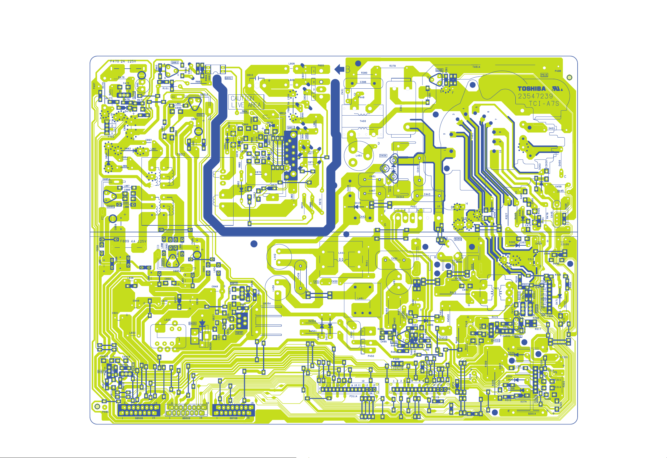
POWER/DEF BOARD PD1087
BOTTOM (FOIL) SIDE
– 33 – – 34 –
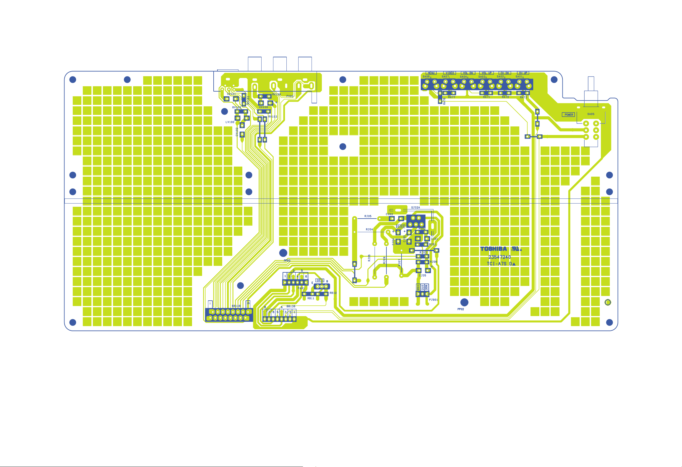
CONT BOARD PD1088-1
BOTTOM (FOIL) SIDE
– 35 – – 36 –
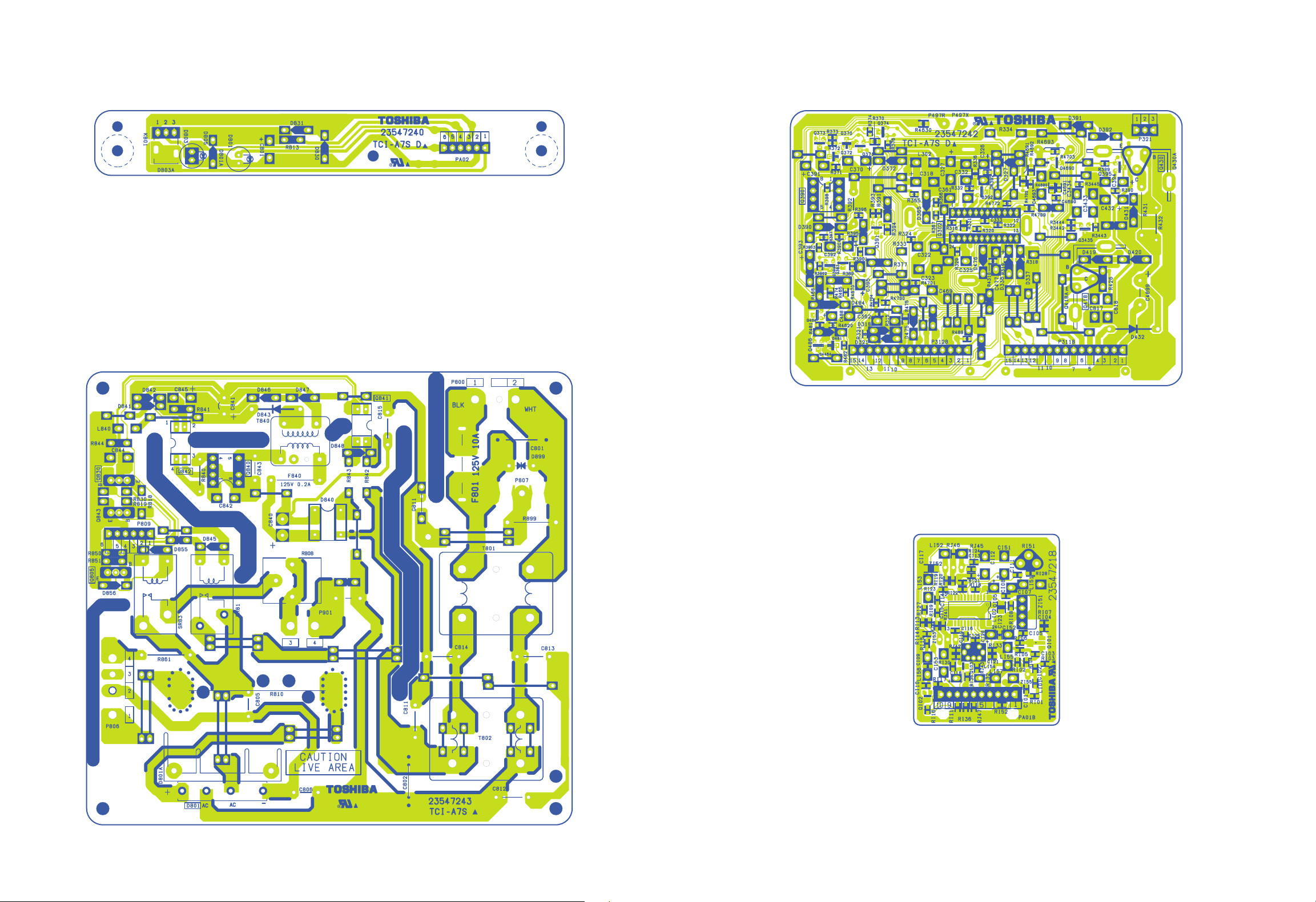
LED BOARD PD1088-2
BOTTOM (FOIL) SIDE
AC-IN BOARD PD1091
BOTTOM (FOIL) SIDE
VERT BOARD PD1090
BOTTOM (FOIL) SIDE
IF BOARD PD1022B
BOTTOM (FOIL) SIDE
– 37 – – 38 –

CRT-D/SVM BOARD PD1089
BOTTOM (FOIL) SIDE
– 39 –

TERMINAL VIEW OF TRANSISTORS
B
C
E
2SD2253
(old)
2SC5243
B
C
E
RN2203
RN2201
RN2004
RN1203
RN1204
SPECIFIC INFORMATIONS
RN2204
RN1205
RN1202
RN1201
B
C
E
2SC3852
2SD1763A
2SC1569
2SC4544
2SA1788
2SA1306
2SA1186A
B
C
E
2SD1554
2SD2253
2SD1556
2SC5143
2SC5570
2SD2553
B
C
E
2SC752GTM
2SC2482
2SC2655
2SC4721P
ON4409
B
C
E
2SC752
2SA562TM
2SA1015
2SC1815
2SC2878
2SC1740S
2SC2120
2SA9335
E
C
B
2SA1788
B
C
E
– 40 –

SCHEMATIC DIAGRAM
MODEL : 34HX83
WARNING: BEFORE SERVICING THIS CHASSIS, READ THE "X-RAY RADIATION PRECAUTION", "SAFETY
PRECAUTION" AND "PRODUCT SAFETY NOTICE" ON THE MANUAL FOR THIS MODEL.
CAUTION: The international hazard symbols "*" in the schematic diagram and the parts list designate components
which have special characteristics important for safety and should be replaced only with types identical to those in the
original circuit or specified in the parts list. The mounting position of replacements is to be identical with originals.
Before replacing any of these components, read carefully the PRODUCT SAFETY NOTICE on the MANUAL for this
model. Do not degrade the safety of the receiver through improper servicing.
NOTE:
1. RESISTOR Resistance is shown in ohm [K = 1.000, M = 1.000.000]. All resistors are 1/6W and 5%
tolerance carbon resistor, unless otherwise noted as the following marks.
1/2R = Metal or Metal oxide of 1/2 watt 1/2S = Carbon compsistion of 1/2 watt
1RF = Fuse resistor of 1 watt 10W = Cement of 10 watt
K = ±10% G = ±2% F = ±1%
2. CAPACITOR Unless otherwise noted in schematic, all capacitor values less than 1 are expressed in
?F, and the values more than 1 in pF.
All capacitors are ceramic 50V, unless otherwise noted as the following marks.
Electolytic capacitor Mylar capacitor
3. The parts indicated with " * " have special characteristics, and should be replaced with identical parts only.
4. Voltages read with DIGITAL MULTI-METER from point indicated to chassing ground, using a color bar signal with all
controls at normal, line voltage 120 volts.
5. Waveforms are taken receiving color bar signal with enough sensitivity.
6. Voltage reading shown are nominal values and may vary ±20% except H.V.
SCHEMATIC DIAGRAM STRUCTURE:
SIGNAL Circuit Sheet assignment [ SHEET - 1 ] .................. 1/25
POWER / DEF Circuit BANKAN [ SHEET - 1/6 ] ............. 13/25
CRT DRIVE / SVM Circuit CRT DRIVE [ SHEET - 1/2 ] ............. 19/25
VERTICAL Circuit ................................................................................................. 21/25
AC INPUT Circuit ................................................................................................. 22/25
IF Circuit ................................................................................................................ 23/25
CONTROL Circuit ................................................................................................. 24/25
LED Circuit ............................................................................................................ 25/25
AV-1 [ SHEET - 2 ] .................. 2/25
AV-2 [ SHEET - 3 ] .................. 3/25
PIP [ SHEET - 4 ].................. 4/25
Maicon [ SHEET - 5 ] .................. 5/25
BEP [ SHEET - 7 ] .................. 6/25
BEP2 [ SHEET - 8 ] .................. 7/25
LOWB-REG [ SHEET - 9 ].................. 8/25
AUDIO OUT [ SHEET - 10 ] ................ 9/25
IF [ SHEET - 11 ] .............. 10/25
BANKAN [ SHEET - 98 ] .............. 11/25
BB CONNECTER [ SHEET - 99 ] .............. 12/25
H-DEF [ SHEET - 2/6 ] ............. 14/25
V-DEF [ SHEET - 3/6 ] ............. 15/25
MAIN-POWER [ SHEET - 4/6 ] ............. 16/25
SUB-POWER [ SHEET - 5/6 ] ............. 17/25
DQF / OPC / OTHER [ SHEET - 6/6 ] ............. 18/25
SVM [ SHEET - 2/2 ] ............. 20/25
– 41 –

H001(MAIN)
KEY
CONTROL
ANT
IN
VIDEO
INPUT 3
VIDEO
INPUT 1
VIDEO/AUDIO
OUTPUT
DV/HD
CP IN
Q302
E/W
CORRECTION
Q402
H DRIVE
Q301
V OUTPUT
-27V
Q370
I
2
C Bus Line
R371
+200V
SCREEN
FOCUS
HIGH VOLTAGE
VH
HEATER
Q862
PHOTO-COUPLER
F801 T801
T840
SR81
D840
D801
Q801
10A
CONVERTER
TRANS
VOLTAGE REG.
OVER VOLTAGE
OVER HEAT
PROTECTOR
AUDIO OUT
Q610
SRS
QD01
R
RL
R
L
L WOOFER
W
Q510
CHROMA
VIDEO
DEF.
A
B
QA02
MEMORY
KEY
CONTROL
QV01 SIGNAL SW
VAR
AUDIO
+25V
QA01
MICROPROCESSOR
VIDEO
INPUT 2
Q843
SW
Q840
Q835
5V2
2A
F470
T862
R883
D883
D884
Q404
H OUTPUT
RED OUTPUT
GREEN OUTPUT
BLUE OUTPUT
FBT
T461
+132V
I
2
C-BUS LINE
POWER/DEF UNIT
LOW/VERT AND
CRT DRIVE UNIT
Q901, Q903, Q905
V901
CRT
HY01
TIF
H003
RF-SW
Q420
SCAN-
PRO.
QV12
SIG SW
Q835
SPECIFIC INFORMATIONS
CIRCUIT BLOCK DIAGRAM
– 42 –

SPECIFICATIONS
Television System
NTSC standard
Channel Coverage
VHF: 2 through 13
UHF: 14 through 69
Cable TV: Mid band (A-8 through A-1, A through I)
Super band (J through W)
Hyper band (AA through ZZ, AAA, BBB)
Ultra band (65 through 94, 100 through
125)
Power Source
120 V AC, 60 Hz
Power Consumption
150 W (average)
Audio Power
10 W + 10 W + 13 W sub-woofer
Speaker Type
Two 6 x 12 cm + one 10 cm round sub-woofer
Video/Audio Terminals
S-VIDEO INPUT
Y : 1 V(p-p), 75 ohm, negative sync.
C : 0.286 V(p-p) (burst signal), 75 ohm
VIDEO/AUDIO INPUT
VIDEO: 1 V(p-p), 75 ohm, negative sync.
AUDIO: 150 mV(rms) (30% modulation equiva-
lent, 47 k ohm)
®
ColorStream
(component video) INPUT
Y : 1V(p-p), 75 ohm
R: 0.7 V(p-p), 75 ohm
P
PB: 0.7 V(p-p), 75 ohm
AUDIO: 150 mV(rms), 47 k ohm
VIDEO/AUDIO OUTPUT
VIDEO: 1 V(p-p), 75 ohm, negative sync.
AUDIO: 150 mV(rms) (30% modulation equiva-
lent, 4.7 k ohm)
VARIABLE AUDIO OUTPUT
0–300 mV(rms) (30% modulation equivalent, 4.7
k ohm)
AUDIO CENTER CHANNEL INPUT
300 mV(rms) (30% modulation equivalent, 10 k
ohm)
DVI/HDCP INPUT
HDCP compliant
E-EDID* 1.3 compliant
DVI-D uncompressed, high-speed, digital singlelink connection
Suggested scan rates: 1080i, 480p, 480i
Dimensions
Width 36-13/16 inches (935 mm)
Height 24-39/64 inches (625 mm)
Depth 23-25/32 inches (604 mm)
Mass
75.7kg
Supplied Accessories
Remote Control with 2 size “AA” alkaline batteries
Optional Stand
ST34W63
Design and specifications are subject to change without
notice.
_________
* E-EDID = Enhanced-Extended Display Identification
SPECIFIC INFORMATIONS
* Please refer to owner's manual in detail.
– 43 –
– END –

TOSHIBA CORPORATION
1-1, SHIBAURA 1-CHOME, MINATO-KU, TOKYO 105-8001, JAPAN
 Loading...