TOSHIBA 2SK2615 Service manual

现货库存、技术资料、百科信息、热点资讯,精彩尽在鼎好!
A
TOSHIBA Field Effect Transistor Silicon N Channel MOS Type (L2−π−MOSV)
2SK2615
2SK2615
DC−DC Converter, Relay Drive and Motor Drive
Applications
z Low drain−source ON resistance : R
z High forward transfer admittance : |Y
z Low leakage current : I
z Enhancement mode : Vth = 0.8~2.0 V (VDS = 10 V, ID = 1 mA)
= 100 μA (max) (VDS = 60 V)
DSS
Absolute Maximum Ratings
Characteristics Symbol Rating Unit
Drain−source voltage V
Drain−gate voltage (RGS = 20 kΩ) V
Gate−source voltage V
Drain current
Drain power dissipation PD 0.5 W
Drain power dissipation (Note 2) PD 1.5 W
Channel temperature Tch 150 °C
Storage temperature range T
Note 1: Ensure that the channel temperature does not exceed 150°C.
Note 2: Mounted on a ceramic substrate (25.4 mm × 25.4 mm × 0.8 mm)
DC (Note 1) ID 2
Pulse (Note 1) I
DS (ON)
(Ta = 25°C)
DSS
DGR
GSS
DP
stg
= 0.23 Ω (typ.)
| = 2.0 S (typ.)
fs
60 V
60 V
±20 V
6
−55~150 °C
A
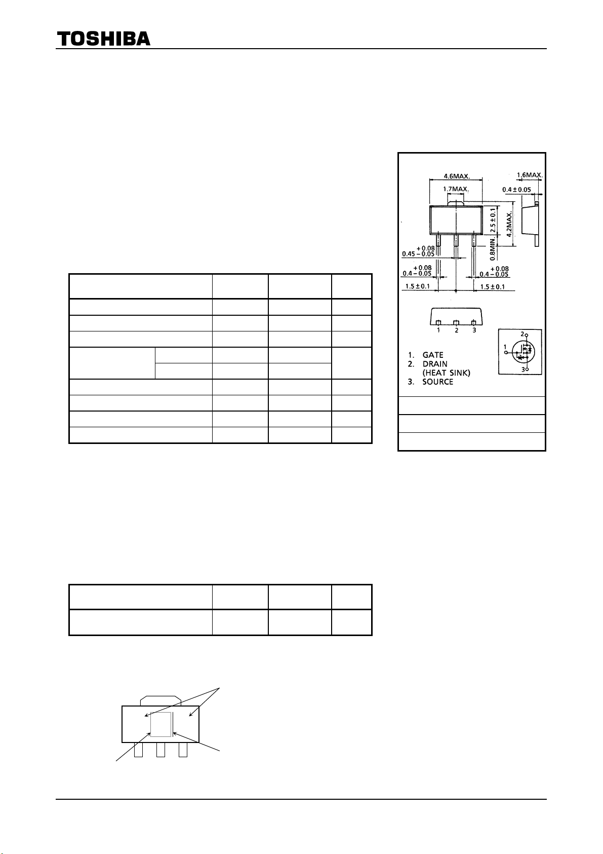
Unit: mm
JEDEC ―
JEITA ―
TOSHIBA 2-5K1B
Weight: 0.05 g (typ.)
Note 3: Using continuously under heavy loads (e.g. the application of high temperature/current/voltage and the significant change
in temperature, etc.) may cause this product to decrease in the reliability significantly even if the operating conditions (i.e.
operating temperature/current/voltage, etc.) are within the absolute maximum ratings. Please design the appropriate
reliability upon reviewing the Toshiba Semiconductor Reliability Handbook (“Handling Precautions”/Derating Concept and
Methods) and individual reliability data (i.e. reliability test report and estimated failure rate, etc).
Thermal Characteristics
Characteristics Symbol Max Unit
Thermal resistance, channel to
ambient
This transistor is an electrostatic-sensitive device.
Please handle with caution.
Marking
Lot No.
Z A
R
Part No. (or abbreviation code)
line indicates
lead (Pb)-free package or
lead (Pb)-free finish.
250 °C / W
th (ch−a)
1
2006-11-17

2SK2615
Electrical Characteristics
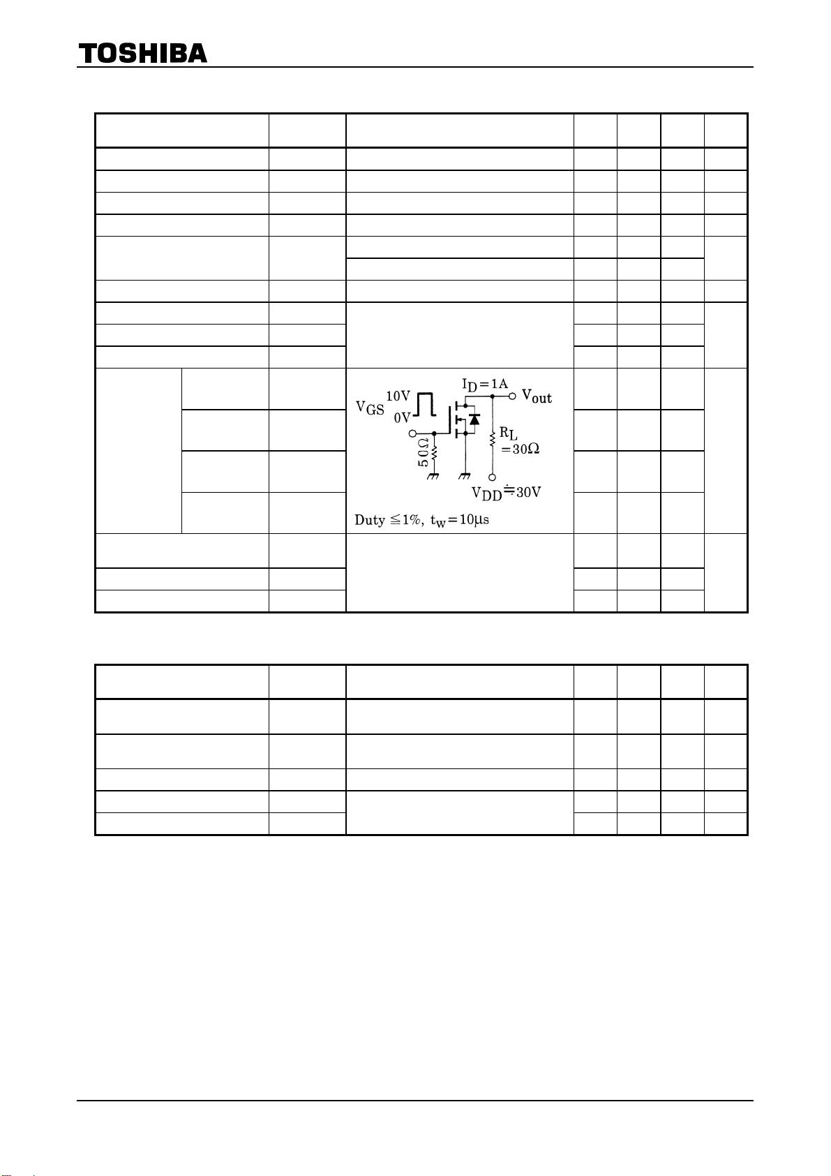
Characteristics Symbol Test Condition Min Typ. Max Unit
Gate leakage current I
Drain cut−off current I
Drain−source breakdown voltage V
Gate threshold voltage V
Drain−source ON resistance R
Forward transfer admittance |Yfs| VDS = 10 V, ID = 1 A 1.0 2.0 — S
Input capacitance C
Reverse transfer capacitance C
Output capacitance C
Rise time tr — 25 —
Turn−on time ton — 30 —
Switching time
Fall time tf — 50 —
(Ta = 25°C)
GSS
DSS
(BR) DSS
th
DS (ON)
— 150 —
iss
— 25 —
rss
oss
VGS = ±16 V, VDS = 0 V — — ±10 μA
VDS = 60 V, VGS = 0 V — — 100 μA
ID = 10 mA, VGS = 0 V 60 — — V
VDS = 10 V, ID = 1 mA 0.8 — 2.0 V
VGS = 4 V, ID = 1 A — 0.33 0.44
VGS = 10 V, ID = 1 A — 0.23 0.30
V
= 10 V, VGS = 0 V, f = 1 MHz
DS
— 70 —
Ω
pF
ns
Turn−off time t
Total gate charge (gate−source
plus gate−drain)
Gate−source charge Qgs — 4.6 —
Gate−drain (“miller”) Charge Qgd
— 150 —
off
— 6.0 —
Q
g
V
≈ 48 V, VGS = 10 V, ID = 2 A
DD
— 1.4 —
Source−Drain Ratings and Characteristics
Characteristics Symbol Test Condition Min Typ. Max Unit
Continuous drain reverse current
(Note 1)
Pulse drain reverse current
(Note 1)
Forward voltage (diode) V
Reverse recovery time t
Reverse recovery charge Q
— — — 2 A
I
DR
— — — 6 A
I
DRP
IDR = 2 A, VGS = 0 V — — −1.5 V
DSF
rr
IDR = 2 A, VGS = 0 V
/ dt = 50 A / μs
dI
rr
DR
(Ta = 25°C)
— 100 — ns
— 40 — nC
nC
2
2006-11-17
 Loading...