Page 1

现货库存、技术资料、百科信息、热点资讯,精彩尽在鼎好!
TOSHIBA Field Effect Transistor Silicon N Channel MOS Type (F-MOSIII)
2SK2613
2SK2613
Switching Regulator Applications, DC-DC Converter and
Motor Drive Applications
· Low drain-source ON resistance: R
DS (ON)
· High forward transfer admittance: ïY
· Low leakage current: I
= 100 µA (max) (VDS = 800 V)
DSS
= 1.4 Ω (typ.)
ï = 6.0 S (typ.)
fs
· Enhancement-model: Vth = 2.0~4.0 V (VDS = 10 V, ID = 1 mA)
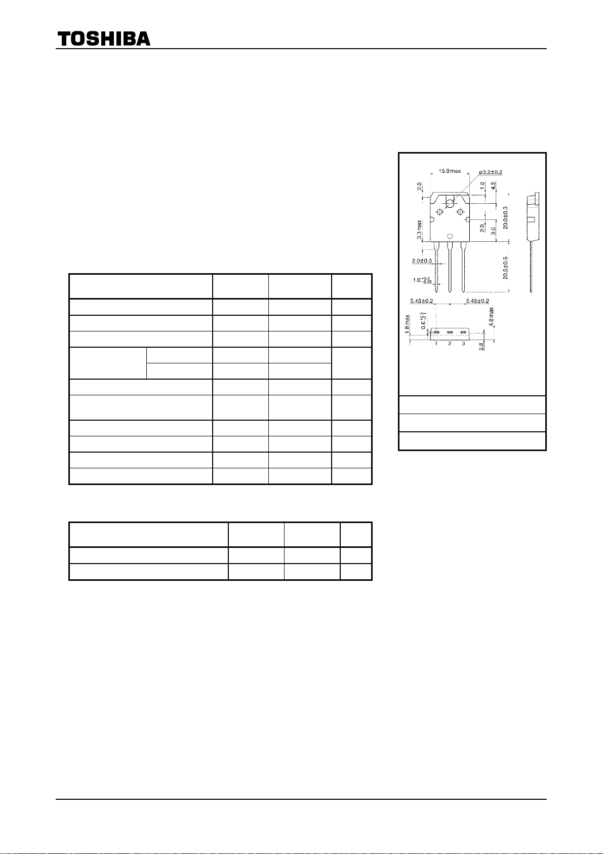
Maximum Ratings
Characteristics Symbol Rating Unit
Drain-source voltage V
Drain-gate voltage (RGS = 20 kW) V
Gate-source voltage V
Drain current
Drain power dissipation (Tc = 25°C) P
Single pulse avalanche energy
(Note 2)
Avalanche current IAR 8 A
Repetitive avalanche energy (Note 3) EAR 15 mJ
Channel temperature Tch 150 °C
Storage temperature range T
(Ta ==== 25°C)
DC (Note 1) I
Pulse (Note 1) I
DSS
DGR
GSS
DP
E
D
AS
stg
D
1000 V
1000 V
±30 V
8
24
150 W
910 mJ
-55~150 °C
A
Thermal Characteristics
1. GATE
2. DRAIN (HEAT SINK)
3. SOURSE
JEDEC ―
JEITA ―
TOSHIBA 2−16C1B
Weight: 4.6 g (typ.)
Unit: mm
Characteristics Symbol Max Unit
Thermal resistance, channel to case R
Thermal resistance, channel to ambient R
0.833 °C/W
th (ch-c)
50 °C/W
th (ch-a)
Note 1: Please use devices on condition that the channel temperature is below 150°C.
Note 2: VDD = 90 V, Tch = 25°C, L = 26.3 mH, RG = 25 W, IAR = 8 A
Note 3: Repetitive rating: Pulse width limited by max junction temperature
This transistor is an electrostatic sensitive device. Please handle with caution.
1
2002-08-09
Page 2

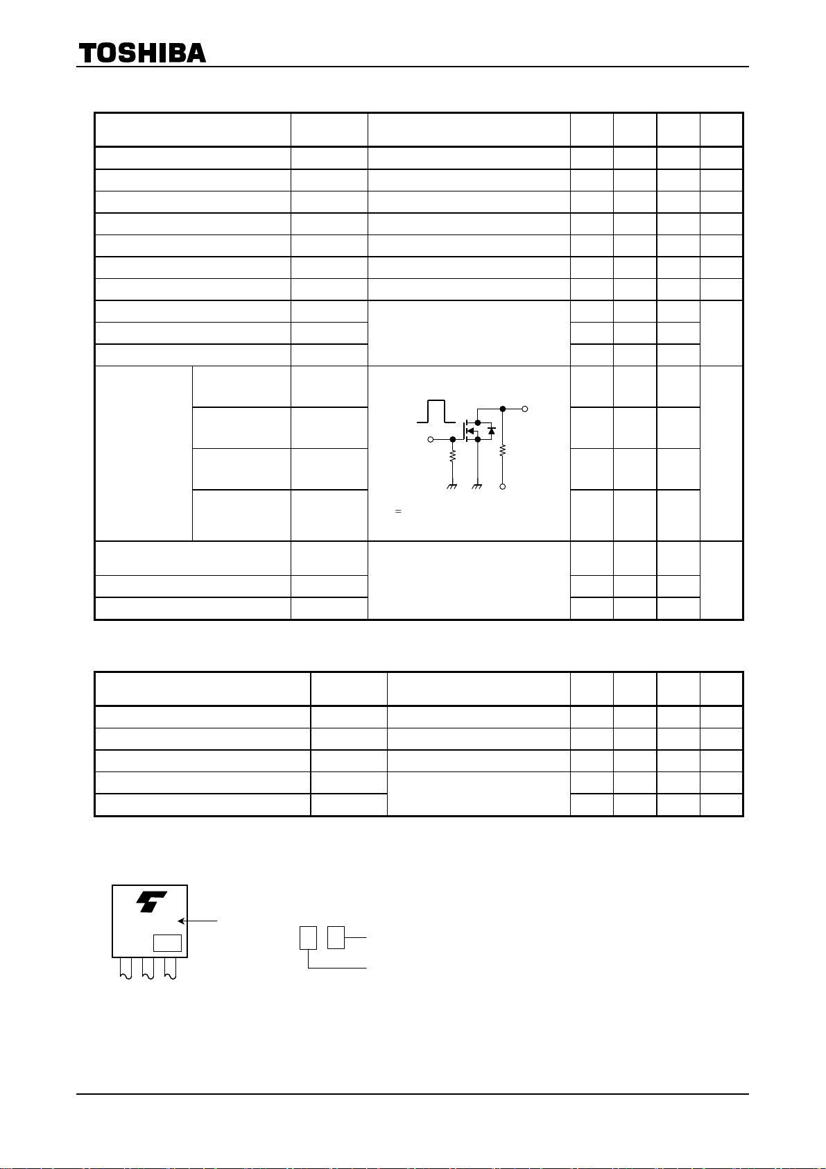
Electrical Characteristics (Ta ==== 25°C)
Characteristics Symbol Test Condition Min Typ. Max Unit
2SK2613
Gate leakage current I
Drain-source breakdown voltage V
Drain cut-OFF current I
Drain-source breakdown voltage V
Gate threshold voltage Vth VDS = 10 V, ID = 1 mA 2.0 ¾ 4.0 V
Drain-source ON resistance R
Forward transfer admittance ïYfsï VDS = 20 V, ID = 4 A 2.0 6.0 ¾ S
Input capacitance C
Reverse transfer capacitance C
Output capacitance C
Rise time tr ¾ 20 ¾
Turn-ON time ton ¾ 40 ¾
Switching time
Fall time tf ¾ 30 ¾
Turn-OFF time t
Total gate charge
(gate-source plus gate-drain)
Gate-source charge Qgs ¾ 40 ¾
Gate-drain (“miller”) charge Qgd
VGS = ±30 V, VDS = 0 V ¾ ¾ ±10 mA
GSS
(BR) GSSIG
DSS
(BR) DSSID
DS (ON)
¾ 2000 ¾
iss
¾ 30 ¾
rss
oss
off
Q
¾ 65 ¾
g
= ±10 mA, VDS = 0 V ±30 ¾ ¾ V
VDS = 800 V, VGS = 0 V ¾ ¾ 100 mA
= 10 mA, VGS = 0 V 1000 ¾ ¾ V
VGS = 10 V, ID = 4 A ¾ 1.4 1.7 W
VDS = 25 V, VGS = 0 V, f = 1 MHz
10 V
V
GS
0 V
Duty<1%, tw = 10 ms
~
V
400 V, V
-
DD
= 4 A
I
D
4.7 9
V
DD
= 10 V, ID = 8 A
GS
V
OUT
RL = 100 W
~
400 V
-
¾ 200 ¾
¾ 100 ¾
¾ 25 ¾
Source-Drain Ratings and Characteristics
(Ta ==== 25°C)
pF
ns
nC
Characteristics Symbol Test Condition Min Typ. Max Unit
Continuous drain reverse current (Note 1) IDR ¾ ¾ ¾ 8 A
Pulse drain reverse current (Note 1) I
Forward voltage (diode) V
Reverse recovery time trr ¾ 1600 ¾ ms
Reverse recovery charge Qrr
¾ ¾ ¾ 24 A
DRP
IDR = 8 A, VGS = 0 V ¾ ¾ -1.9 V
DSF
= 8 A, VGS = 0 V,
I
DR
/dt = 100 A/ms
dI
DR
¾ 24 ¾ mC
Marking
K2613
Type
※
※ Lot Number
Month (starting from alphabet A)
Year (last number of the christian era)
2
2002-08-09
Page 3

2SK2613
10
Common source
Tc = 25°C
Pulse test
8
(A)
D
6
4
Drain current I
2
0
4 0
Drain-source voltage VDS (V)
20
Common source
VSD = 20 V
Pulse test
16
(A)
D
12
8
Drain current I
4
0
2 0
Gate-source voltage VGS (V)
100
ï (S)
fs
10
1
Forward transfer admittance ïY
Tc = -55°C
– VDS
I
D
10 15
VGS = 4.75 V
8 12 16
– VGS
I
D
25
100
Tc = -55°C
4 6 8
ïY
ï - ID
fs
Common source
VSD = 20 V
Pulse test
25
100
6.0
5.75
5.5
5.25
5.0
I
– VDS
20
Common source
Tc = 25°C
Pulse test
16
(A)
D
12
8
Drain current I
4
20
0
200
Drain-source voltage VDS (V)
D
15
10
6.5
6.25
6.0
5.75
5.5
5.25
VGS = 5.0 V
40 60 80
100
– V
V
DS
20
16
(V)
DS
12
8
4
Drain-source voltage V
10
0
40
Gate-source voltage VGS (V)
GS
Common source
Tc = 25°C
Pulse test
ID = 8 A
4
2
8 12 16
20
DS (ON)
- ID
Common source
Tc = 25°C
Pulse test
R
10
5
3
(9)
DS (ON)
0.5
R
0.3
1
VGS = 10,15
Drain-source on resistance
0.1
0.1
1
Drain current ID (A)
10
100
0.1
0.1 0.3 1 3 10 30
Drain current ID (A)
3
2002-08-09
Page 4

2SK2613
5
Common source
DS (ON)
VGS = 10 V
Pulse test
4
3
(W)
2
1
Drain-source on resistance R
0
-40 -80
Case temperature Tc (°C)
10000
Capacitance – V
1000
100
Capacitance C (pF)
Common source
VGS = 0 V
f = 1 MHz
Tc = 25°C
10
1 0.1 100010
Drain-source voltage VDS (V)
200
160
(W)
D
120
80
40
Drain power dissipation P
R
- Tc
DS (ON)
ID = 8 A
2
0 40 80
DS
C
iss
C
oss
C
rss
100
- Tc
P
D
- VDS
I
100
10
(A)
DR
1
4
10
-0.20
Drain-source voltage VDS (V)
160
0.1
Drain reverse current I
0
DR
3
1
VGS = 0, -1 V
-0.6
-0.4 -0.8 -1.0
-1.2
- Tc
V
th
5
4
(V)
th
3
2
1
Gate threshold voltage V
0
-80 0 40 80 120 160-40
Case temperature Tc (°C)
Common source
V
= 10 V
DS
ID = 1 mA
Pulse test
Dynamic input/output characteristics
500
400
(V)
DS
300
200
100
Drain-source voltage V
V
DS
V
VDS = 100 V
GS
400
Common source
ID = 8 A
Tc = 25°C
Pulse test
200
20
16
(V)
GS
12
8
4
Gate-source voltage V
0
0 80 120 20040 160
Case temperature Tc (°C)
0
0 40 60 80 10020
Total gate charge Qg (nC)
4
0
2002-08-09
Page 5

2SK2613
m
10
/R
r
1
Duty = 0.5
0.2
0.1
th (ch-a)
0.1
0.05
0.02
th (t)
0.01
0.01
Single pulse
Normalized transient thermal impedance
0.001
10 m 100 m 1 m 10 m 100
Pulse width tw (S)
100
50
ID max (pulsed) *
30
ID max (continuous)
10
5
(A)
3
D
1
0.5
0.3
Drain current I
0.1
* Single nonrepetitive pulse
0.05
Tc = 25°C
0.03
Curves must be derated linearly
with increase in temperature.
0.01
1
Safe operating area
DC Operation
Tc = 25°C
10 3 10030 10000300
Drain-source voltage VDS (V)
100 ms *
1 ms *
V
max
DSS
1000 3000
- tw
r
th
(mJ)
AS
Avalanche energy E
R
= 25 W
G
V
= 90 V, L = 26.3 mH
DD
P
DM
t
T
Duty = t/T
R
= 0.833°C/W
th (ch-c)
110
– Tch
E
1000
800
600
400
200
0
25
50 75 100 125 150
Channel temperature (initial) Tch (°C)
AS
15 V
-15 V
V
Test circuit Wave form
Ε
AS
B
VDSS
I
AR
V
DD
1
2
DS
æ
B
2
IL
×××=
ç
ç
è
B
VDSS
VDSS
ö
÷
÷
-
V
DD
ø
5
2002-08-09
Page 6

2SK2613
A
RESTRICTIONS ON PRODUCT USE
· TOSHIBA is continually working to improve the quality and reliability of its products. Nevertheless, semiconductor
devices in general can malfunction or fail due to their inherent electrical sensitivity and vulnerability to physical
stress. It is the responsibility of the buyer, when utilizing TOSHIBA products, to comply with the standards of
safety in making a safe design for the entire system, and to avoid situations in which a malfunction or failure of
such TOSHIBA products could cause loss of human life, bodily injury or damage to property.
In developing your designs, please ensure that TOSHIBA products are used within specified operating ranges as
set forth in the most recent TOSHIBA products specifications. Also, please keep in mind the precautions and
conditions set forth in the “Handling Guide for Semiconductor Devices,” or “TOSHIBA Semiconductor Reliability
Handbook” etc..
· The TOSHIBA products listed in this document are intended for usage in general electronics applications
(computer, personal equipment, office equipment, measuring equipment, industrial robotics, domestic appliances,
etc.). These TOSHIBA products are neither intended nor warranted for usage in equipment that requires
extraordinarily high quality and/or reliability or a malfunction or failure of which may cause loss of human life or
bodily injury (“Unintended Usage”). Unintended Usage include atomic energy control instruments, airplane or
spaceship instruments, transportation instruments, traffic signal instruments, combustion control instruments,
medical instruments, all types of safety devices, etc.. Unintended Usage of TOSHIBA products listed in this
document shall be made at the customer’s own risk.
· The information contained herein is presented only as a guide for the applications of our products. No
responsibility is assumed by TOSHIBA CORPORATION for any infringements of intellectual property or other
rights of the third parties which may result from its use. No license is granted by implication or otherwise under
any intellectual property or other rights of TOSHIBA CORPORATION or others.
· The information contained herein is subject to change without notice.
000707EA
6
2002-08-09
 Loading...