TOSHIBA 2SK2611 Service manual

现货库存、技术资料、百科信息、热点资讯,精彩尽在鼎好!
TOSHIBA Field Effect Transistor Silicon N Channel MOS Type (π−MOSIII)
2SK2611
2SK2611
DC−DC Converter, Relay Drive and Motor Drive
Applications
z Low drain−source ON resistance : R
DS (ON)
z High forward transfer admittance : |Y
z Low leakage current : I
= 100 μA (max) (VDS = 720 V)
DSS
z Enhancement−mode : Vth = 2.0~4.0 V (VDS = 10 V, ID = 1 mA)
Absolute Maximum Ratings
Characteristics Symbol Rating Unit
Drain−source voltage V
Drain−gate voltage (RGS = 20 kΩ) V
Gate−source voltage V
Drain current
Drain power dissipation (Tc = 25°C) PD 150 W
Single pulse avalanche energy
(Note 2)
Avalanche current IAR 9 A
Repetitive avalanche energy (Note 3) EAR 15 mJ
Channel temperature Tch 150 °C
Storage temperature range T
DC (Note 1) ID 9 A
Pulse (Note 1) I
(Ta = 25°C)
DSS
DGR
GSS
DP
E
AS
stg
= 1.1 Ω (typ.)
7.0 S (typ.)
fs| =
900 V
900 V
±30 V
27 A
663 mJ
−55~150 °C
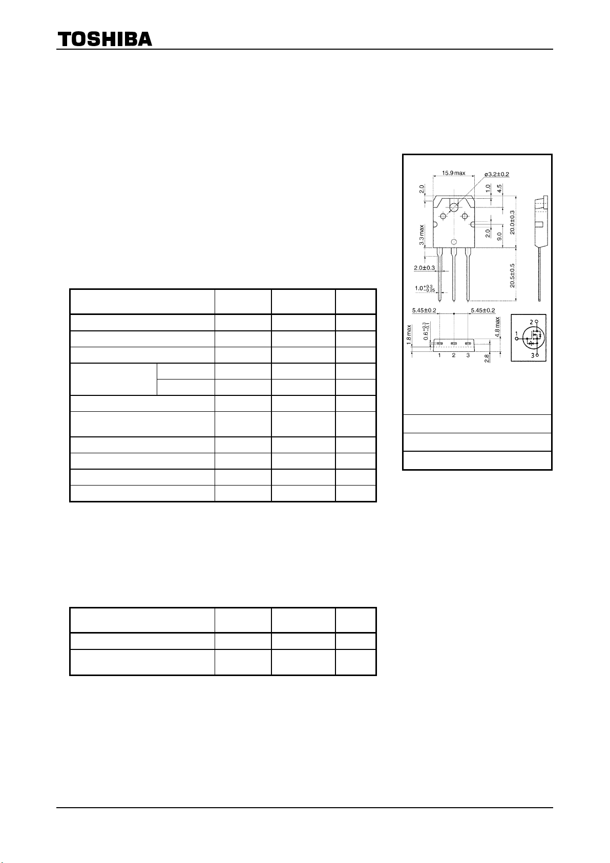
Unit: mm
1. GATE
2. DRAIN (HEAT SINK)
3. SOURCE
JEDEC ―
JEITA SC-65
TOSHIBA 2-16C1B
Weight: 4.6 g (typ.)
Note: Using continuously under heavy loads (e.g. the application of high temperature/current/voltage and the significant change in
temperature, etc.) may cause this product to decrease in the reliability significantly even if the operating conditions (i.e.
operating temperature/current/voltage, etc.) are within the absolute maximum ratings. Please design the appropriate
reliability upon reviewing the Toshiba Semiconductor Reliability Handbook (“Handling Precautions”/Derating Concept and
Methods) and individual reliability data (i.e. reliability test report and estimated failure rate, etc).
Thermal Characteristics
Characteristics Symbol Max Unit
Thermal resistance, channel to case R
Thermal resistance, channel to
ambient
R
Note 1: Please use devices on condition that the channel temperature is below 150°C.
Note 2: VDD = 90 V, Tch = 25°C (initial), L = 15 mH, RG = 25 Ω, IAR = 9 A
Note 3: Repetitive rating: Pulse width limited by maximum channel temperature
This transistor is an electrostatic sensitive device.
Please handle with caution.
0.833 °C / W
th (ch−c)
50 °C / W
th (ch−a)
1
2006-11-10

2SK2611
A
Electrical Characteristics
Characteristics Symbol Test Condition Min Typ. Max Unit
Gate leakage current I
Gate−source breakdown voltage V
Drain cut−off current I
Drain−source breakdown voltage V
Gate threshold voltage V
Drain−source ON resistance R
Forward transfer admittance |Yfs| VDS = 15 V, ID = 4 A 3.0 7.0 — S
Input capacitance C
Reverse transfer capacitance C
Output capacitance C
Rise time tr — 25 —
Turn−on time ton — 60 —
Switching time
Fall time tf — 20 —
(Ta = 25°C)
GSS
(BR) GSS
DSS
(BR) DSS
th
DS (ON)
— 2040 —
iss
— 45 —
rss
oss
VGS = ±30 V, VDS = 0 V — — ±10 μA
IG = ±10 μA, VDS = 0 V ±30 — — V
VDS = 720 V, VGS = 0 V — — 100 μA
ID = 10 mA, VGS = 0 V 900 — — V
VDS = 10 V, ID = 1 mA 2.0 — 4.0 V
VGS = 10 V, ID = 4 A — 1.1 1.4 Ω
V
= 25 V, VGS = 0 V, f = 1 MHz
DS
— 190 —
pF
ns
Turn−off time t
Total gate charge (gate−source
plus gate−drain)
Gate−source charge Qgs — 32 —
Gate−drain (“miller”) Charge Qgd
— 95 —
off
— 58 —
Q
g
V
≈ 400 V, VGS = 10 V, ID = 9 A
DD
— 26 —
nC
Source−Drain Ratings and Characteristics
Characteristics Symbol Test Condition Min Typ. Max Unit
Continuous drain reverse current
(Note 1)
Pulse drain reverse current
(Note 1)
Forward voltage (diode) V
Reverse recovery time t
Reverse recovery charge Q
— — — 9 A
I
DR
— — — 27 A
I
DRP
IDR = 9 A, VGS = 0 V — — −1.9 V
DSF
rr
rr
IDR = 9 A, VGS = 0 V, dIDR / dt = 100 A / μs
(Ta = 25°C)
— 1.6 — μs
— 20 — μC
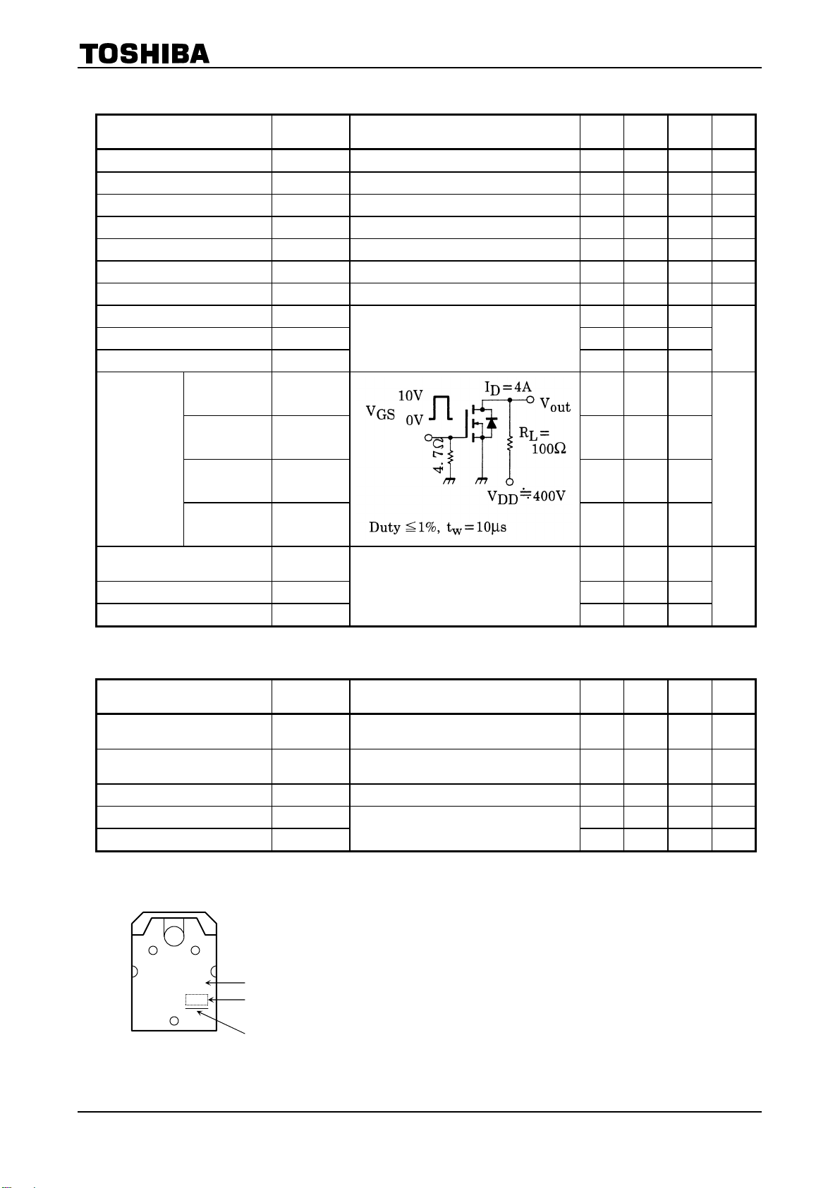
Marking
TOSHIBA
K2611
Part No. (or abbreviation code)
Lot No.
line indicates
lead (Pb)-free package or
lead (Pb)-free finish.
2
2006-11-10
 Loading...