


FILE NO. 020-200405
DOCUMENT CREATED IN JAPAN, Jun., 2004
SERVICE MANUAL
LCD Color Television
26HL84

TABLE OF CONTENTS
SERVICE SAFETY PRECAUTIONS.................................................................................................................................... 3
HANDLING THE LCD MODULE .......................................................................................................................................... 5
SERVICE MODE.................................................................................................................................................................. 7
TROUBLESHOOTING DIAGNOSIS FUNCTION ................................................................................................................ 8
LOCATION OF CONTROLS ..............................................................................................................................................10
LAYOUT OF MAJOR BOARDS ......................................................................................................................................... 12
MECHANICAL DISASSEMBLY ......................................................................................................................................... 13
EXPLODED VIEW ............................................................................................................................................................. 26
PACKING DISASSEMBLY ................................................................................................................................................. 30
CHASSIS AND CABINET REPLACEMENT PARTS LIST ................................................................................................. 31
PC BOARDS BOTTOM VIEW ........................................................................................................................................... 39
CIRCUIT BLOCK DIAGRAM ............................................................................................................................................. 53
SPECIFICATIONS.......................................................................................................................................................... END
APPENDIX:
SCHEMATIC DIAGRAM
– 2 –
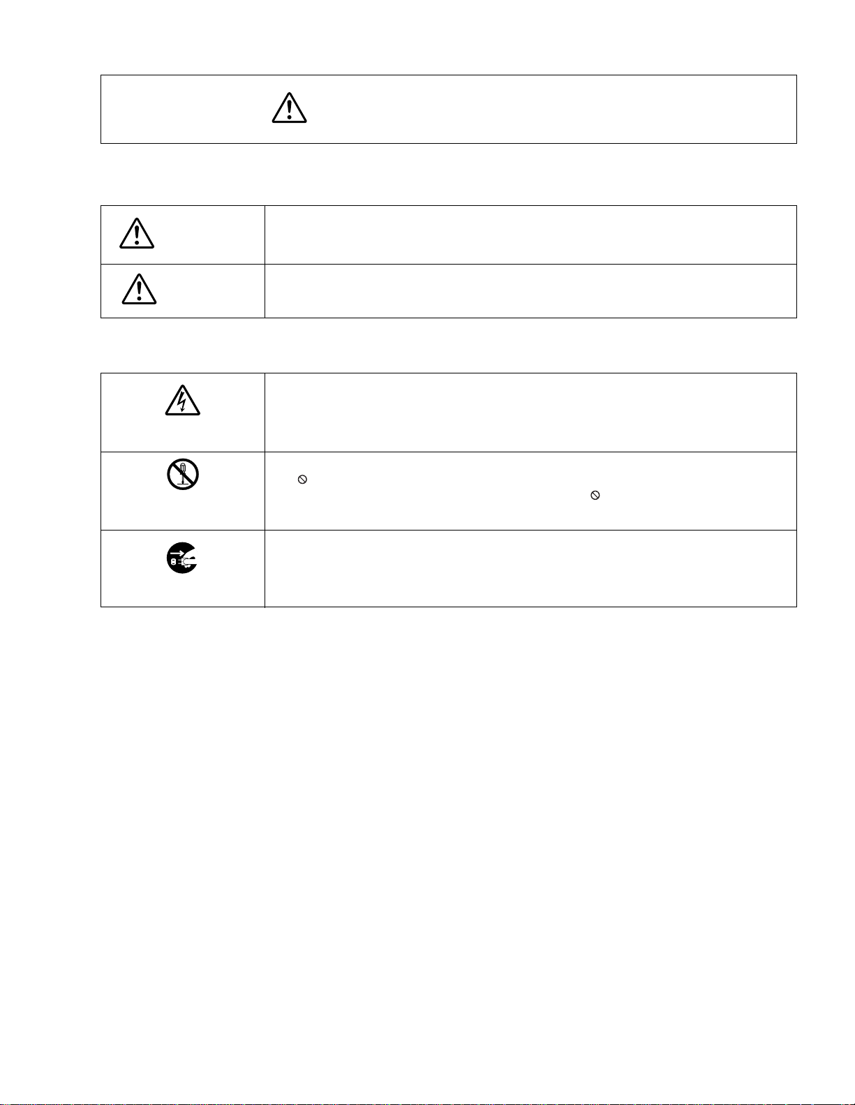
SERVICE SAFETY PRECAUTIONS
• The caution items shown here describe major safety issues and should always be observed.
• The meanings of the various indications are as follows.
WARNING
CAUTION
*Physical damage means major damage to a home, furnishings and other possessions.
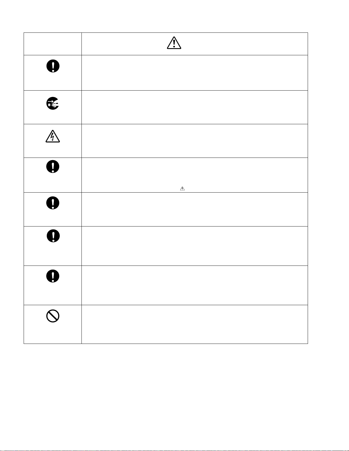
Examples of marks
SHOCK HAZARD
PROHIBIT DISASSEM-
BLING
UNPLUG
Indicates a hypothetical situation in which service personnel and nearby third parties, or even
end users due to a product defect after the service operation is completed, could possibly be in
danger of injury or even death in the event of operational error.
Indicates a hypothetical situation in which service personnel and nearby third parties, or even
end users after the service operation is completed, could possibly be in danger of injury, or
where there could be physical damage in the event of operational error.
The " indicates caution (including danger and warning).
The actual meaning of this caution is indicated inside the " or nearby illustrations or text.
The example shown to the left indicates the danger of "electrical shock".
indicates a forbidden action.
The
The actual meaning of this caution is indicated inside the or nearby illustrations or text.
The example shown to the left indicates that disassembly is forbidden.
The - indicates a forced action (an action that must be performed).
The actual meaning of this forced action is indicated by - or nearby illustrations or text.
The example shown to the left indicates that the power plug must be disconnected.
– 3 –
KEEP CHILDREN
AWAY
UNPULUG
SHOCK HAZARD
USE SPECIFIED
PARTS
CAUTION FOR
WIRING
CAUTION FOR
ASSEMBLING /
WIRING
WARNING
• Always advise users to keep children away.
There is danger of injury to children from tools, disassembled products, etc.
• Always disconnect the power plug before starting work whenever power is not required.
Failure to disconnect the power plug before starting work can result in electrical shock.
• Depending on the model, use an insulation transformer or wear gloves when servicing with the
power on, and disconnect the power plug to avoid electrical shock when replacing parts.
In some cases, alternating current is also impressed in the chassis, so electrical shock is possible if the chassis is contacted with the power on.
• Always use the replacement parts specified for the particular model when making repairs.
The parts used in products have the necessary safety characteristics such as inflammability,
voltage resistance, etc.; therefore, use only replacement parts that have these same characteristics.
Use only the specified parts when the mark is included in a circuit diagram or parts list.
• Parts mounting and routing of the wiring should be the same as that used originally.
For safety purposes, insulating materials such as tubing or tape is sometimes used and printed
circuit boards are sometimes mounted floating.
Also make sure that wiring is routed and clamped to avoid parts that generate heat and which
use high voltage. Always follow the original scheme.
• After a repair has been completed, reassemble all disassembled parts, and route and reconnect the wiring, in accordance with the original scheme.
Do not allow internal wiring to be pinched by cabinets, panels, etc.
Any error in reassembly or wiring can result in electrical leakage, flame, etc., and may be
hazardous.
CHECK INSULATION
RESISTANCE
PROHIBIT
REMODELING
• After completing the work, disconnect the power plug from the outlet, remove the antenna, turn
on the power switch. Then, use a 500V insulation resistance meter to check the insulation
resistance of the antenna terminal, other metallic parts and between the prongs of the power
plug to make sure that the insulation resistance is 1M Ω or more.
The set will require inspection and repair if the insulation resistance is below this value.
• Never remodel the product in any way.
Remodeling can result in improper operation, malfunction, or electrical leakage and flame,
which may be hazardous
– 4 –
HANDLING THE LCD MODULE
Safety Precautions
In the event that the screen is damaged or the liquid crystal
(fluid) leaks, do not breathe in or drink this fluid. Also, never
touch this fluid.
Such actions could cause toxicity or skin irritation. If this fluid
should enter the mouth, rinse the mouth thoroughly with water. If the fluid should contact the skin or clothing, wipe off
with alcohol, etc., and rinse thoroughly with water. If the fluid
should enter the eyes, immediately rinse the eyes thoroughly
with running water.
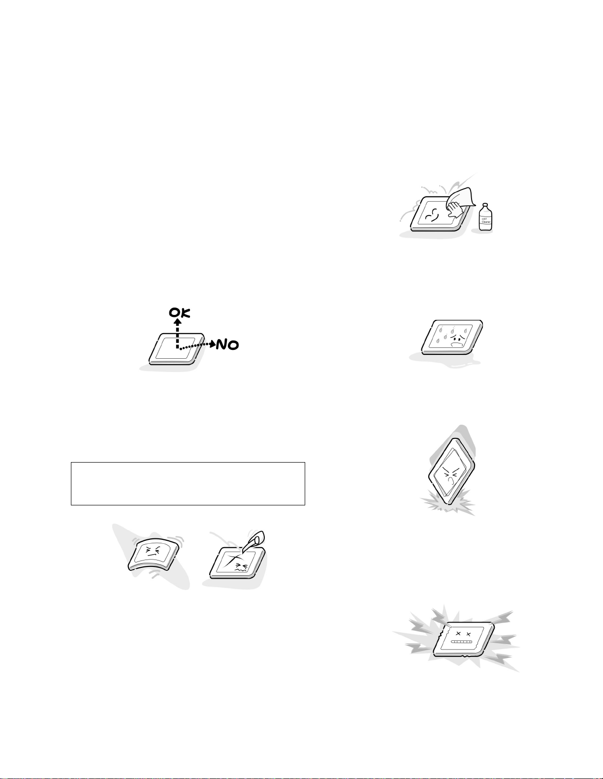
Precautions for Handling the LCD Module
The LCD module can easily be damaged during disassembly
or reassembly; therefore, always observe the following precautions when handling the module.
1. When attaching the LCD module to the LCD cover, position it appropriately and fasten at the position where the
display can be viewed most conveniently.
3. If the panel surface becomes soiled, wipe with cotton or a
soft cloth. If this does not remove the soiling, breathe on
the surface and then wipe again.
If the panel surface is extremely solied, use a CRT cleaner
as a cleaner. Wipe off the panel surface by drop the cleaner
on the cloth. Do not drop the cleaner on the panel. Pay
attention not to scratch the panel surface.
4. Leaving water or other fluids on the panel screen for an
extended period of time can result in discoloration or
stripes. Immediately remove any type of fluid from the
screen.
2. Carefully align the holes at all four corners of the LCD
module with the corresponding holes in the LCD cover
and fasten with screws. Do not strongly push on the module because any impact can adversely affect the performance. Also use caution when handling the polarized screen
because it can easily be damaged.
The metal edges of the LCD module
CAUTION
are sharp, so use caution to avoid injury.
5. Glass is used in the panel, so do not drop or strike with
hard objects. Such actions can damage the panel.
6. CMOS-LSI circuitry is used in the LCD module, so avoid
damage due to static electricity. When handling the module, use a wrist ground or anchor ground.
– 5 –
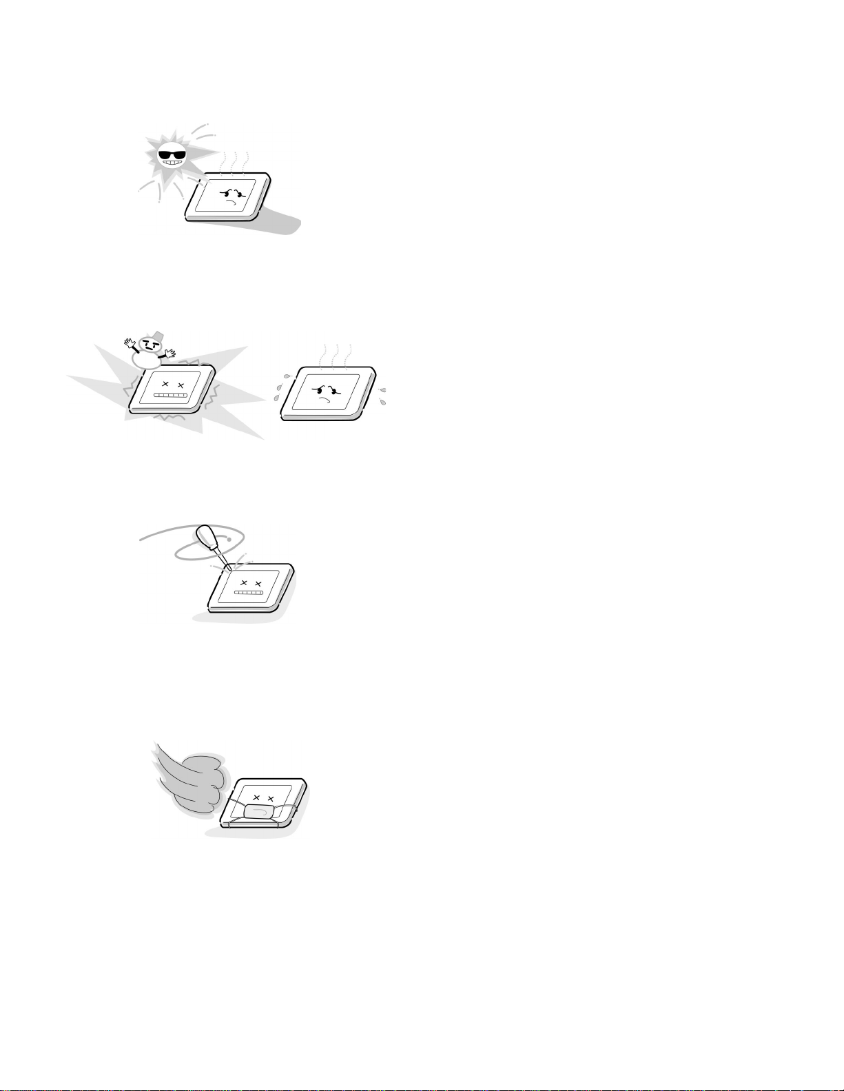
7. Do not expose the LCD module to direct sunlight or strong
ultraviolet rays for an extended period of time.
8. Do not store the LCD module below the temperature conditions described in the specifications. Failure to do so
could result in freezing of the liquid crystal due to cold air
or loss of resilience or other damage.
9. Do not disassemble the LCD module. Such actions could
result in improper operation.
10. When transporting the LCD module, do not use packing
containing epoxy resin (amine) or silicon resin (alcohol or
oxim). The gas generated by these materials can cause
loss of polarity.
– 6 –
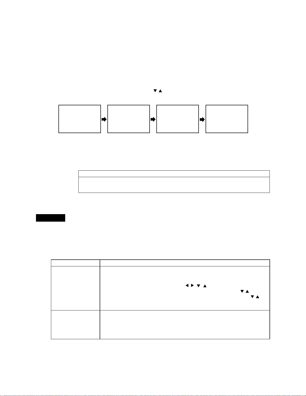
SERVICE MODE
ENTERING TO SERVICE MODE
1) Press the "MUTE" button once on the remote control, "1/2 MUTE" is displayed on the screen.
2) Press the "MUTE" button again, "MUTE" is displayed on the screen.
3) Press the "MENU" button on the TV while pressing the "MUTE" button on the remote control, "S" may appear
on the screen. Then enter to the service mode.
4) Press the "MENU" button on the remote control, adjustment item appears on the screen.
NOTE
Adjustment items may change by pressing the "CH
1) 2) 3) 4)
" buttons on the remote control.
S
1/2 mute
* EXIT FROM SERVICE MODE-Turn off the "POWER" of the TV or remote control.
Built-in signal
.
When press the "INPUT" source selection button on the remote controller during service mode,
generate the built-in test video signal for servicing.
Built-in test video signal (Use for the adjustment such as white balance, etc.)
General broadcasting signal => red monochrome => green monochrome
=> blue monochrome => white signal => black cross bar => built-in signal OFF
mute
(Service mode screen)
RCUT
60H
CAUTION
For the video system adjustment, never attempt to initialize the data unless initial setting data is exceed
incorrectly.
Adjustment items
Brightness correction
(BRTC)
White balance
(RCUT) (GCUT) (BCUT)
Adjustment procedure
1) Receive a general broadcasting program, then press "MENU" button on the
remote control, set the unicolor to minimum (00) and brightness to standard (00)
in order to display the "Setting menu" => "Picture setting" => "Picture adjust-
ment" by pressing the cursor buttons "
2) Select BRTC (brightness correction) using the cursor buttons "CH
remote control, fine adjust the black signal to be black using the "VOL "
buttons on the remote control. After the adjustment, set "unicolor" back to
initialize data.
1) Enter the service mode, press the "INPUT" source setting button on the remote
control to generate the built-in white signal.
2) Adjust the data of items RCUT, GCUT and BCUT for proper white-balanced
picture in low light area.
* For high
light area, GDRV and RDRV items can be adjusted for proper white-balanced picture.
– 7 –
".
" on the
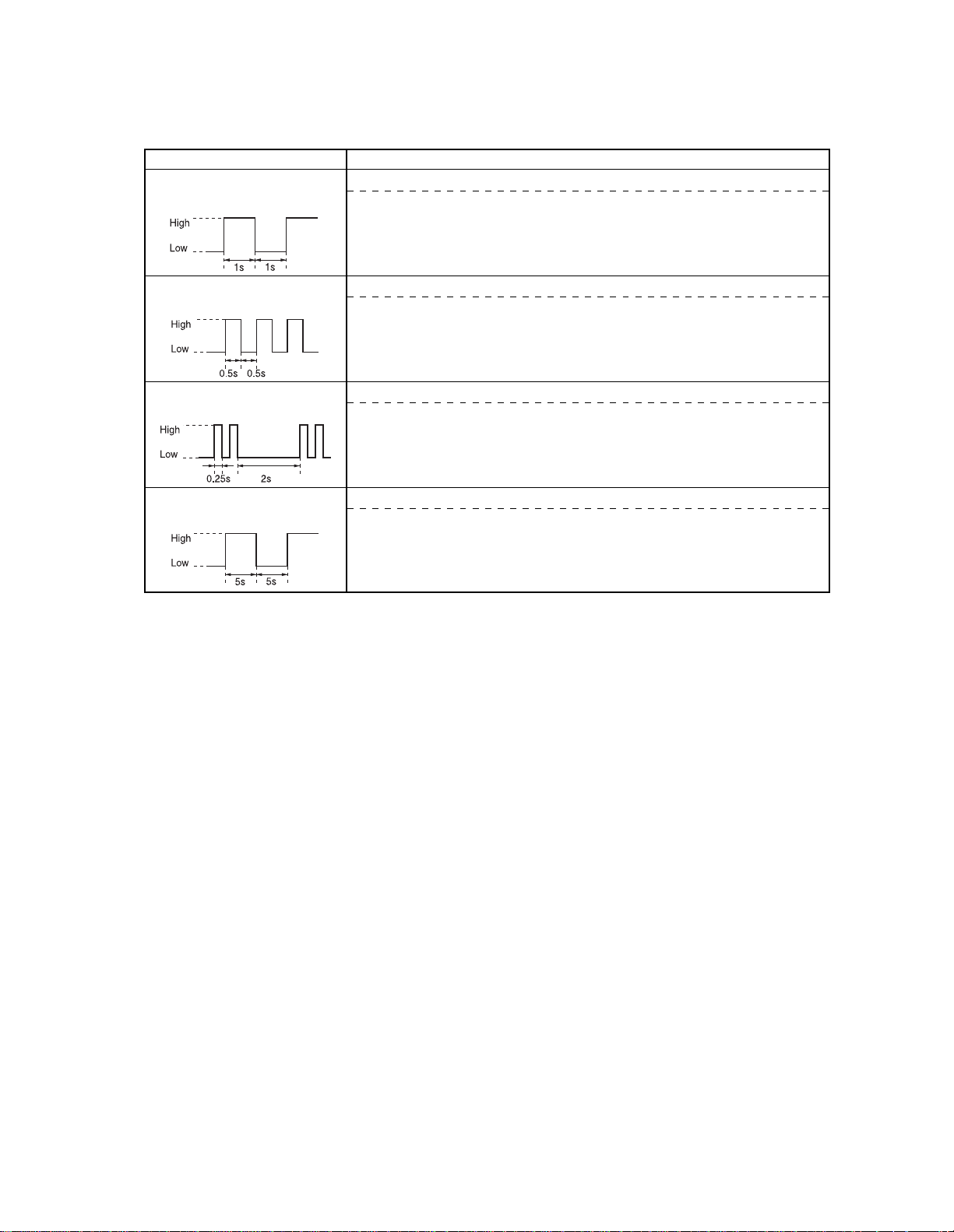
TROUBLESHOOTING DIAGNOSIS FUNCTION
1. DIAGNOSIS FUNCTION FOR LED INDICATION
LED
LED is lit in 1 second at
intervals of 1 second.
Short-circuit detection of BUS line
BUS line may possibly be short-circuit (SDA to SCL), or BUS line (SDA,
SCL) is grounded.
CAUSE
LED is lit in 0.5 at intervals
of 0.5 second.
LED is lit in 0.25 second at
intervals of 2 second.
LED is lit in 5 seconds at
intervals of 5 seconds.
High : Lighting Low : No Lighting
Overcurrent limiter detection
POWER terminal on TV microprocessor becomes LOW at 2 seconds or
more.
Interruption of FAN motor function detection
No. 53 terminal on TV microprocessor becomes HIGH for 30 seconds.
Abnormal sound detection
P4 terminal of QS10 becomes LOW for 15 seconds during Speaker is
activated.
– 8 –
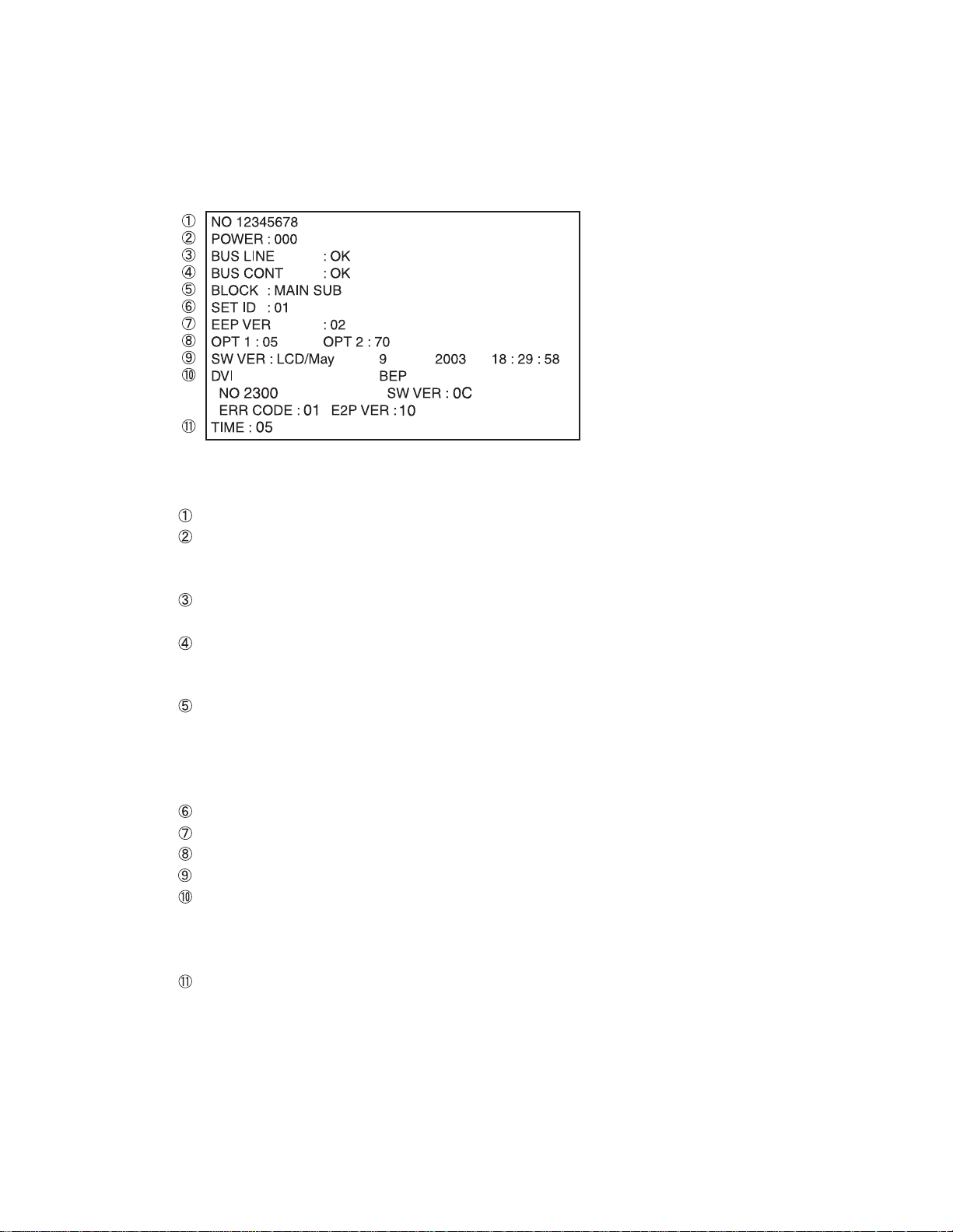
2. SELF DIAGNOSIS FUNCTION
1) Press "9" button on the remote control during display of adjustment menu in the service mode.
2) During diagnosis, the following displays are shown.
<SELF CHECK>
Part number of microprocessor
Operation number of protecting circuit ------"00" is normal.
When indication is other than "00", overcurrent is apt to flow, and circuit parts may possibly be damaged.
BUS LINE ------"OK" is normal.
When indication shows "NG (Green: OK, Red: NG)", the BUS line may possibly be short-circuit.
BUS CONT------"OK" is normal.
When indication shows "Q uuu (Green: OK, Red: NG )", the device with the number may possibly be
damaged.
BLOCK
MAIN : Main picture display --Green indication
Main picture does not display--Red indication
SUB : Sub picture display --Green indication
Sub picture does not display--Red indication
ID number of this unit.
EEP of soft version information
Data number of OPT1 and OPT2
Software version information of host microprocessor (date indication)
DVI NO : DVI number information
DVI ERR CODE : DVI status code number
BEP SW VER : Software version information for BEP microprocessor
BEP E2P VER : Software version information for BEP E2P
Total hour of turn the TV on. (Unit: hour)
*INITIALIZATION OF SELF DIAGNOSIS DATA
1) Enter the service mode, then select any register item.
2) Press and hold the RECALL button on the remote control, then press the CHANNEL up button on the TV. The
initialization has been completed.
– 9 –
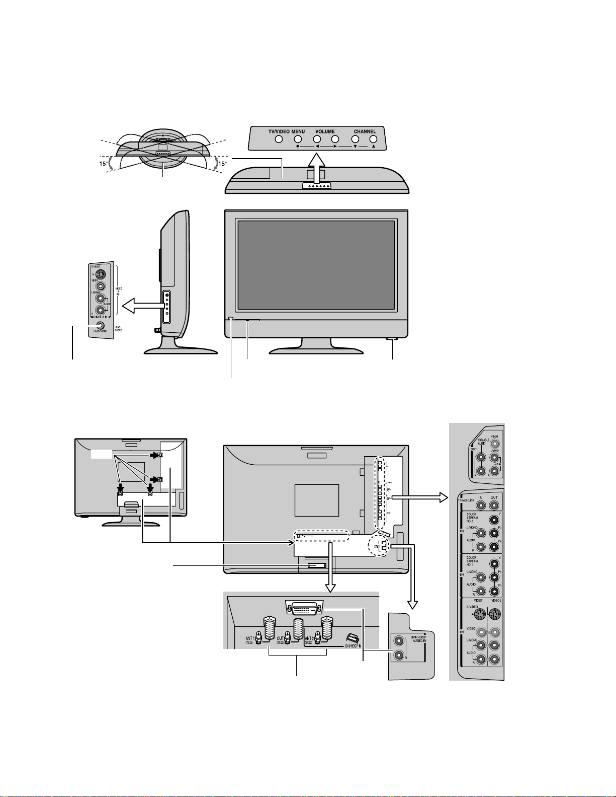
Terminals
(VIDEO 3)
LOCATION OF CONTROLS
Control panel
To p
Swivel base
FrontSide
GENERAL ADJUSTMENTS
POWER
Headphone jack
Back
Push
Remove
the covers
Cable clamper
(Supplied: see page 8)
Power indicator
Remote sensor
POWER
SPECIFIC INFORMATIONS
Terminals
• VIDEO/AUDIO OUT
• VARIABLE AUDIO OUT
Antenna terminals
– 10 –
DVI/HDCP IN
Terminals
• VIDEO 1 IN
• VIDEO 2 IN
• ColorStream HD-1/2
• TheaterLink IN/OUT
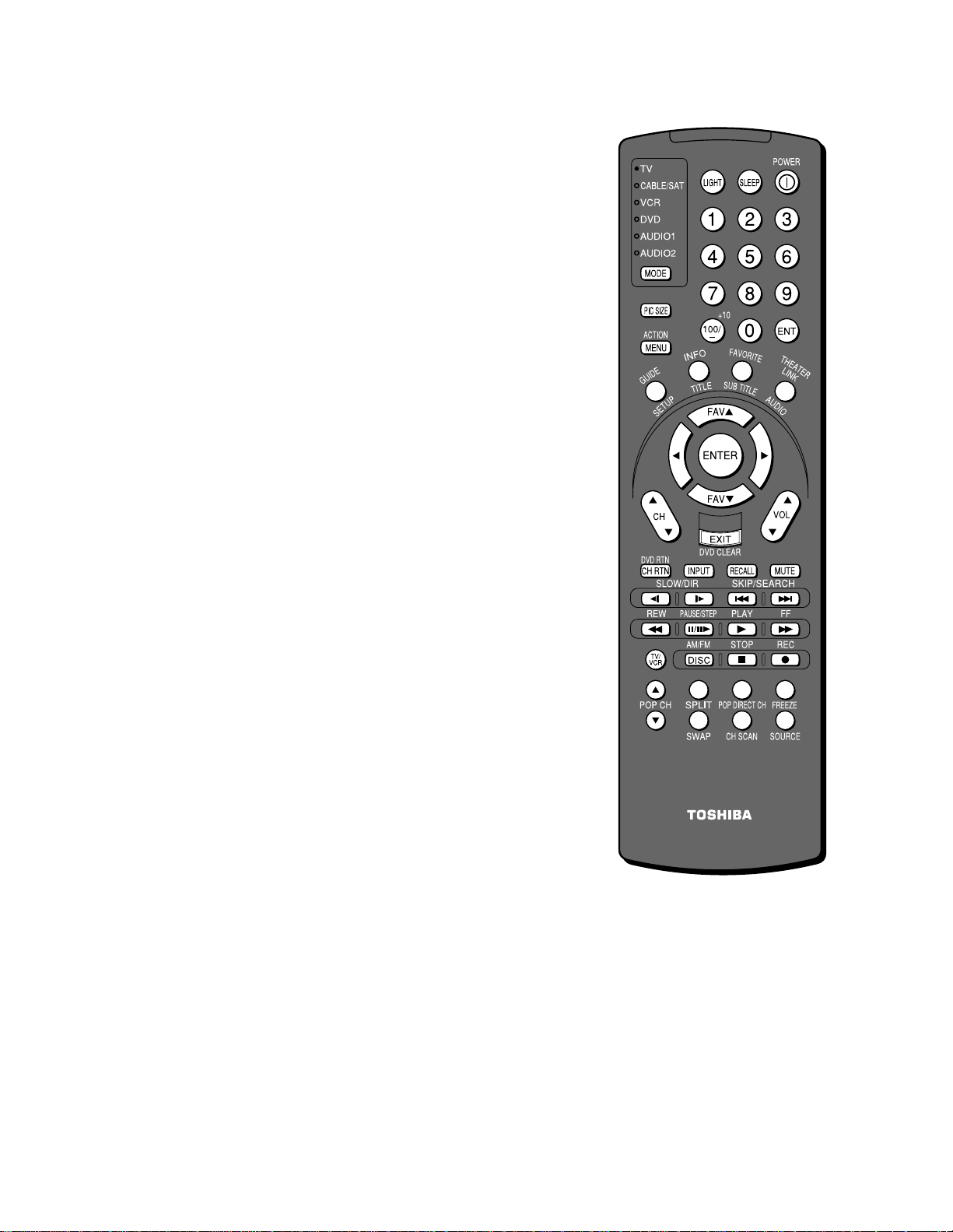
Learning about the remote control
The buttons used for operating the TV only are described here. For a
complete list of the remote control’s functions, see the “Remote
Control functional key chart” on pages 19–20.
POWER turns the TV on and off
SLEEP allows access to the automatic TV shut-off function (page 53)
LIGHT The first press of the LIGHT button lights the keypad and turns
on the Illumination mode. With the Illumination mode on,
pressing any other key lights the keypad for 5 seconds (10 seconds
if you’re in programming mode).
Subsequent presses of the LIGHT button toggle between turning
the Illumination mode on and off.
Channel Numbers (0-9, 100) allow direct access to channels (page 30)
MODE cycles through the six device modes: TV, CABLE/SAT, VCR,
DVD, AUDIO1, and AUDIO2. The mode indicator light will
remain lit for a few seconds (page 21).
PIC SIZE cycles through the five pictures sizes: Natural, Theater Wide 1,
2, 3, and Full (page 34)
FAVORITE allows access to the favorite channel search function (page 41)
MENU allows access to on-screen programming menus (page 26)
ENTER sets programming menu information (page 26)
yz x • select or adjust programming menus (page 26)
FAV yzcycles through favorite channels (page 32)
CH yz cycles through programmed channels (page 29)
VOL yz adjusts the volume level
EXIT exits the programming menus (page 26)
INPUT selects the video input source (page 50)
MUTE mutes the sound (page 54)
RECALL displays on-screen information (page 60)
CH RTN returns to the last viewed channels (page 31)
POP CH yz selects the POP (picture-out-picture) channel (page 38)
SPLIT turns the POP feature on and off (page 38)
CH SCAN
FREEZE freezes the POP picture (page 39)
SWAP switches the main and POP pictures (page 39)
allows access to the programmed channel search function (page 40)
Note:
The error message “Not Available” will appear
if you press a key for a function that is not
available.
POP DIRECT CH allows direct access to POP channels (page 38)
SOURCE selects the POP picture source (page 38)
– 11 –
LAYOUT OF MAJOR BOARDS
U800 POWER MODULE UNIT
U901D POWER SW Board
U901A SIGNAL Board
U902A TN/AOUT Board
U903 SCALER Board
U901E KEY SW Board
U901C AV2 Board
U901G D-REWRITE Board
– 12 –
U901B FRONT/AV Board
U901F LED/RMT Board
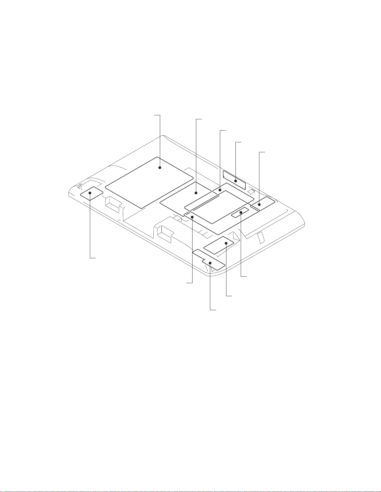
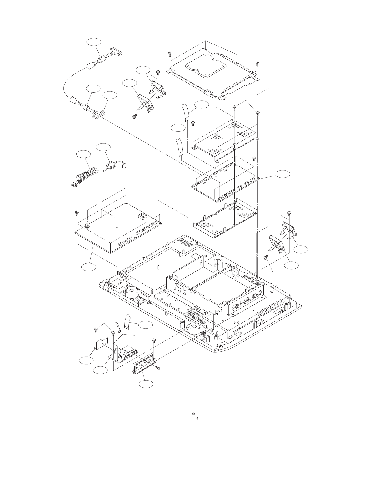
MECHANICAL DISASSEMBLY
• Note: Be sure to lay down the main body (by placing its screen
downward) for disassembly.
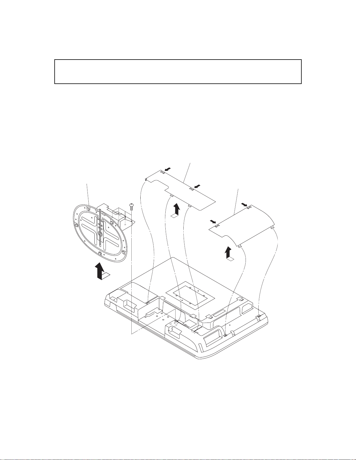
1. Removing the back cover
1) Remove the BC stand cover.
2) Remove the BC terminal cover.
3) Remove 6 screws, then remove the stand.
BC Stand Cover
Stand
BC Terminal Cover
PP 5x12
– 13 –
4) Remove 11 screws (PBI 4x12).
5) Remove 5 screws (PP 3x6).
6) Remove the back cover.
PBI 4x12
PP 3x6
PP 3x8
PP 3x8
Back Cover
– 14 –
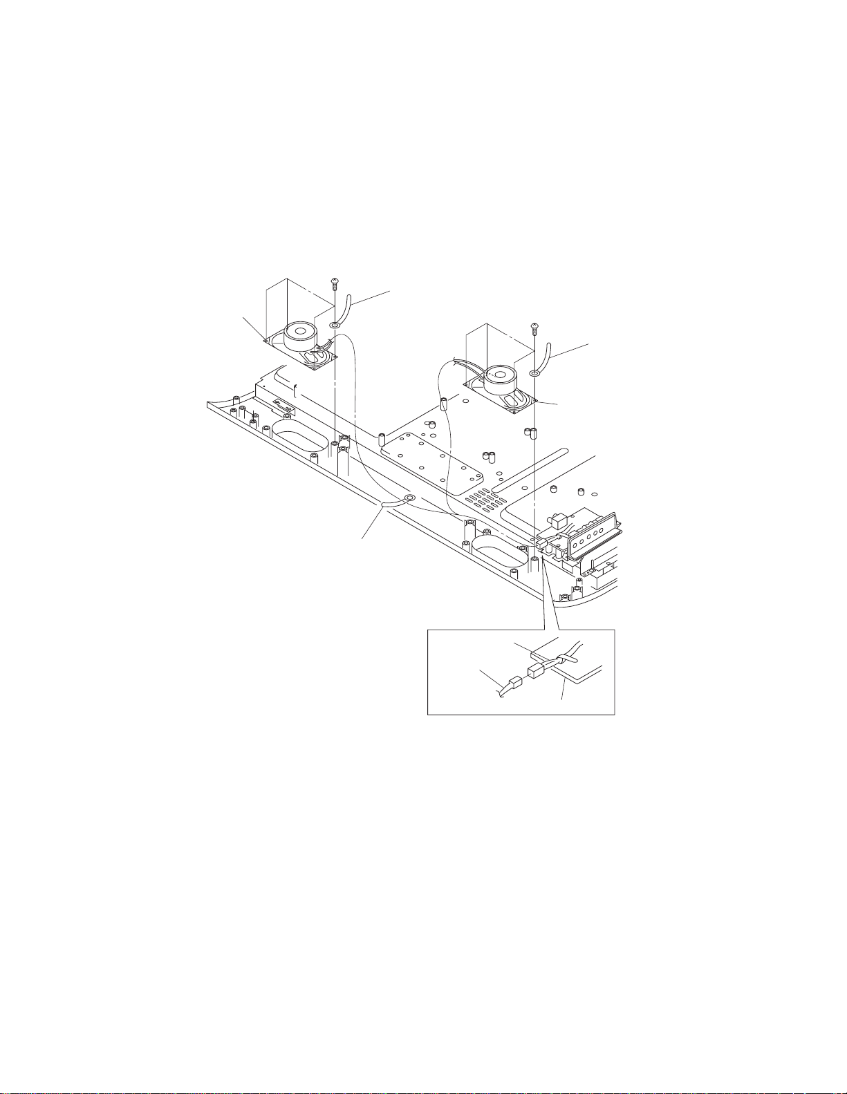
2. Removing the speakers
r
1) Remove the back cover. (Refer to Item 1.)
2) Disconnect the speaker wire harness on the Front/AV board.
3) Remove the wire harness of the 3 wire holders.
4) Remove 4 screws, then remove the left speaker and wire holder.
5) Remove 4 screws, then remove the right speaker and wire holder.
PBI 4x12
Wire holder
Speaker (R)
PBI 4x12
Wire holde
Speaker (L)
Wire holder
Wire harness
Speaker
wire harness
FRONT/AV Board
– 15 –
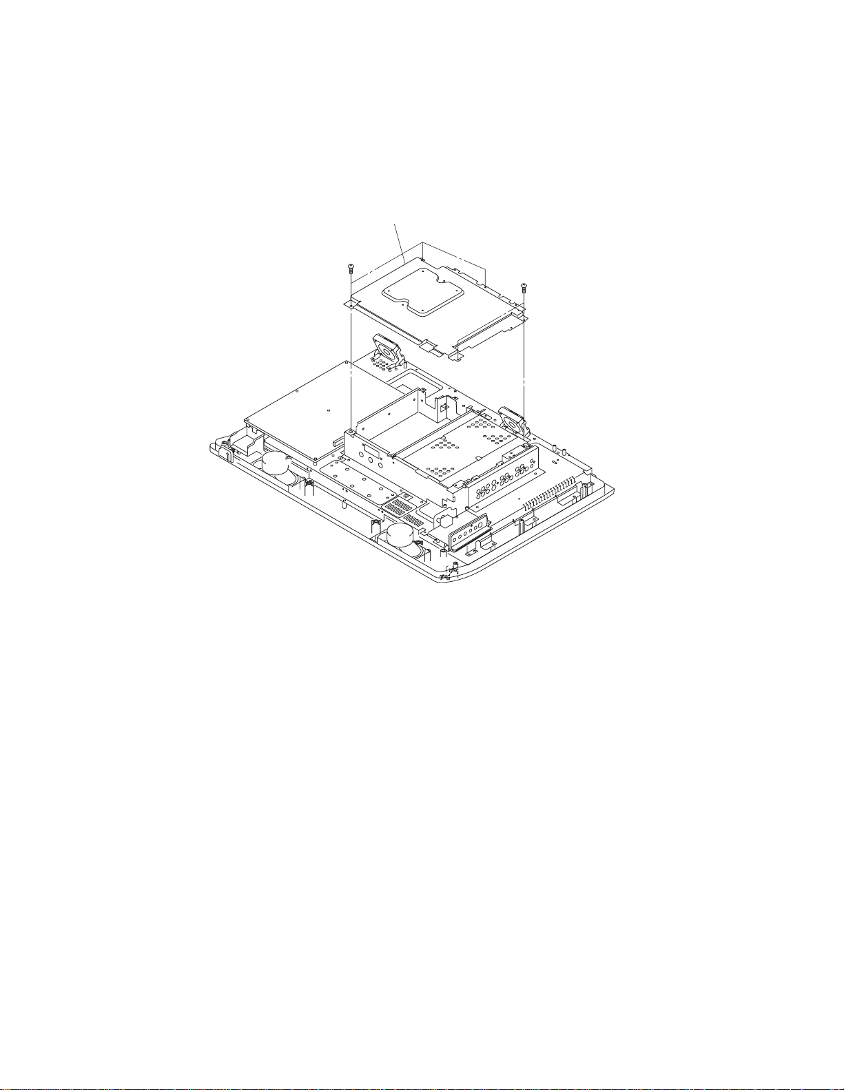
3. Removing the top shield bracket
1) Remove the back cover. (Refer to Item 1.)
2) Remove 5 screws, then remove the top shield bracket.
Top Shield Braket
STP 3x8
STP 3x8
– 16 –
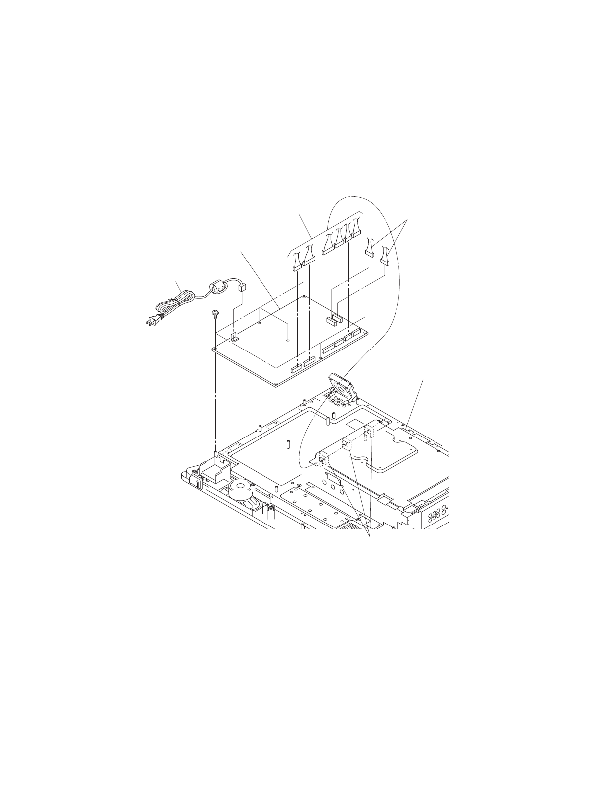
4. Removing the Power Module unit
1) Remove the back cover. (Refer to Item 1.)
2) Disconnect the power cord from the connector.
3) Remove the 3 wire harnesses from the 3 wire clampers on the plate back R.
4) Disconnect the 8 wire harnesses from the 8 connectors on the Power Module unit.
5) Remove 7 screws, then remove the Power Module unit.
Power cord
STP 3x8
Wire Harnesses
POWER MODULE UNIT
Wire Harnesses
Plate Back R
– 17 –
Wire clampers
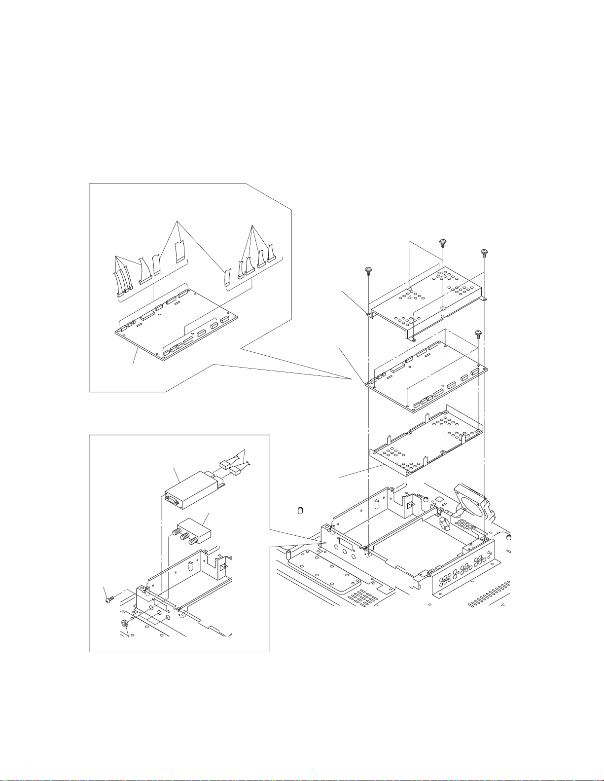
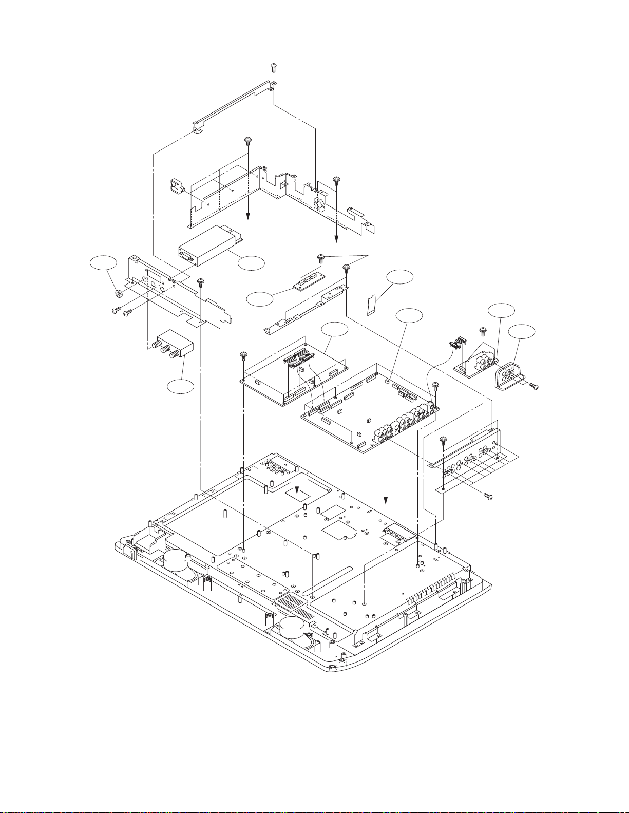
5. Removing the Scaler board
1) Remove the back cover. (Refer to Item 1.)
2) Remove the top shield bracket. (Refer to Item 3.)
3) Remove 4 screws (STP3x6) and 2 screws (STP3x5), then remove the top shield RM.
4) Disconnect the 8 wire harnesses and 2 FFC from the Scaler board.
5) Remove 4 screws (STP3x5), then remove the Scaler board and bottom shield RM.
Wire harnesses
SCALER
board
FFC
DVI MODULE
Wire harnesses
STP 3x5
STP 3x6
STP 3x6
Top shield RM
STP 3x5
SCALER board
Wire harnesses
Bottom
shield RM
BIDT2
3 x10 BZ
ANT
Nuts
– 18 –
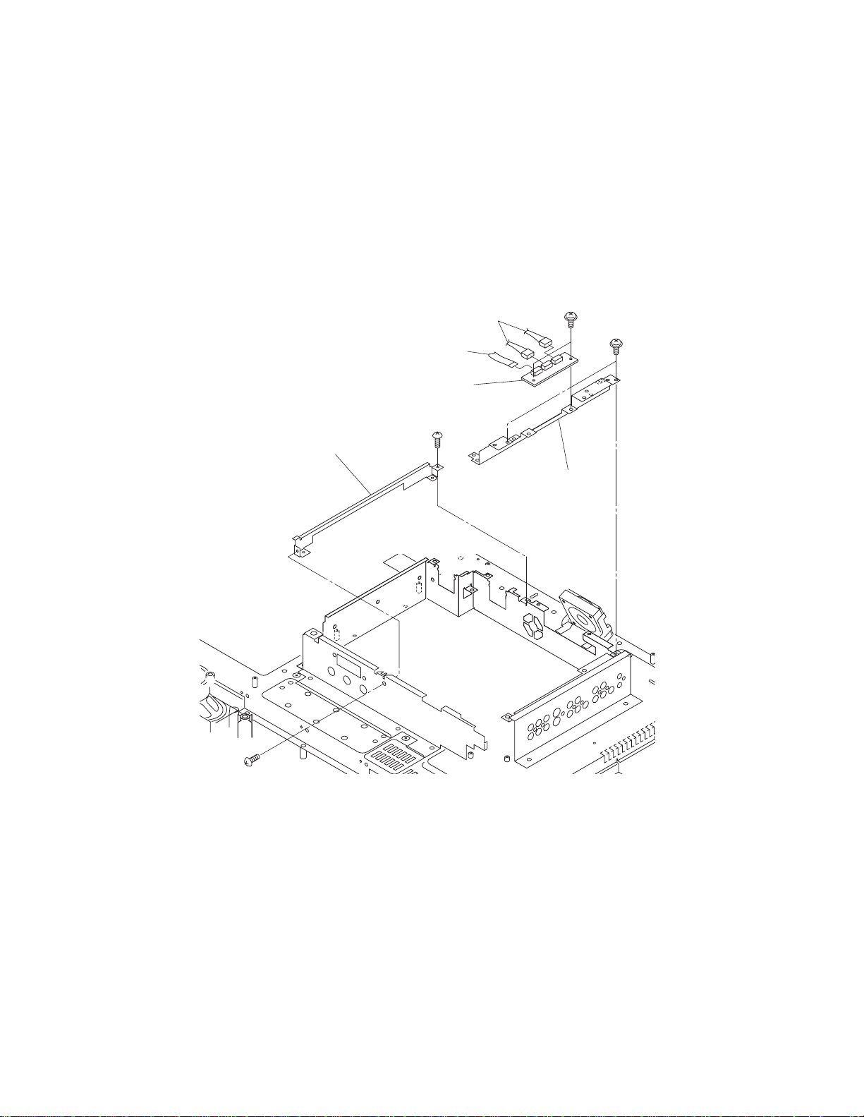
6. Removing the D-Rewrite board
1) Remove the back cover. (Refer to Item 1.)
2) Remove the top shield bracket. (Refer to Item 3.)
3) Remove the Scaler board. (Refer to Item 5.)
4) Remove 2 screws, then remove the D-Rewrite board.
5) Disconnect the 2 wire harnesses and 1 FFC on the D-Rewrite board.
6) Remove 2 screws, then remove the digital unit bracket.
7) Remove 2 screws, then remove the scaler unit bracket.
Scaler unit bracket
Wire harnesses
FFC
D-REWRITE board
STP 3x8
STP 3x8
STP 3x8
Digital unit bracket
PP 3x6
– 19 –
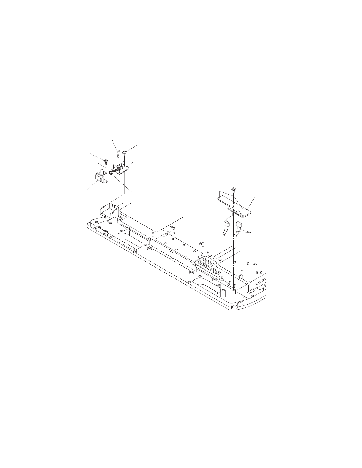
7. Removing the back terminal plate, back bottom plate and back R plate
1) Remove the back cover. (Refer to Item 1.)
2) Remove the top shield bracket. (Refer to Item 3.)
3) Remove the Scaler board. (Refer to Item 5.)
4) Remove the D-Rewrite board. (Refer to Item 6.)
5) Remove 5 screws (BIDT 2 3x10BZ) and 2 screws, then remove the back terminal plate.
6) Remove 2 screws (STP 3x8), 2 hexagon nuts and 1 toothed washer, then remove the back bottom plate.
7) Remove 5 screws (STP 3x8), then remove the back R plate.
STP 3x8
Back plate R
STP 3x8
Back terminal plate
Back bottom plate
STP 3x8
STP 3x8
BIDT2 3x10 BZ
– 20 –
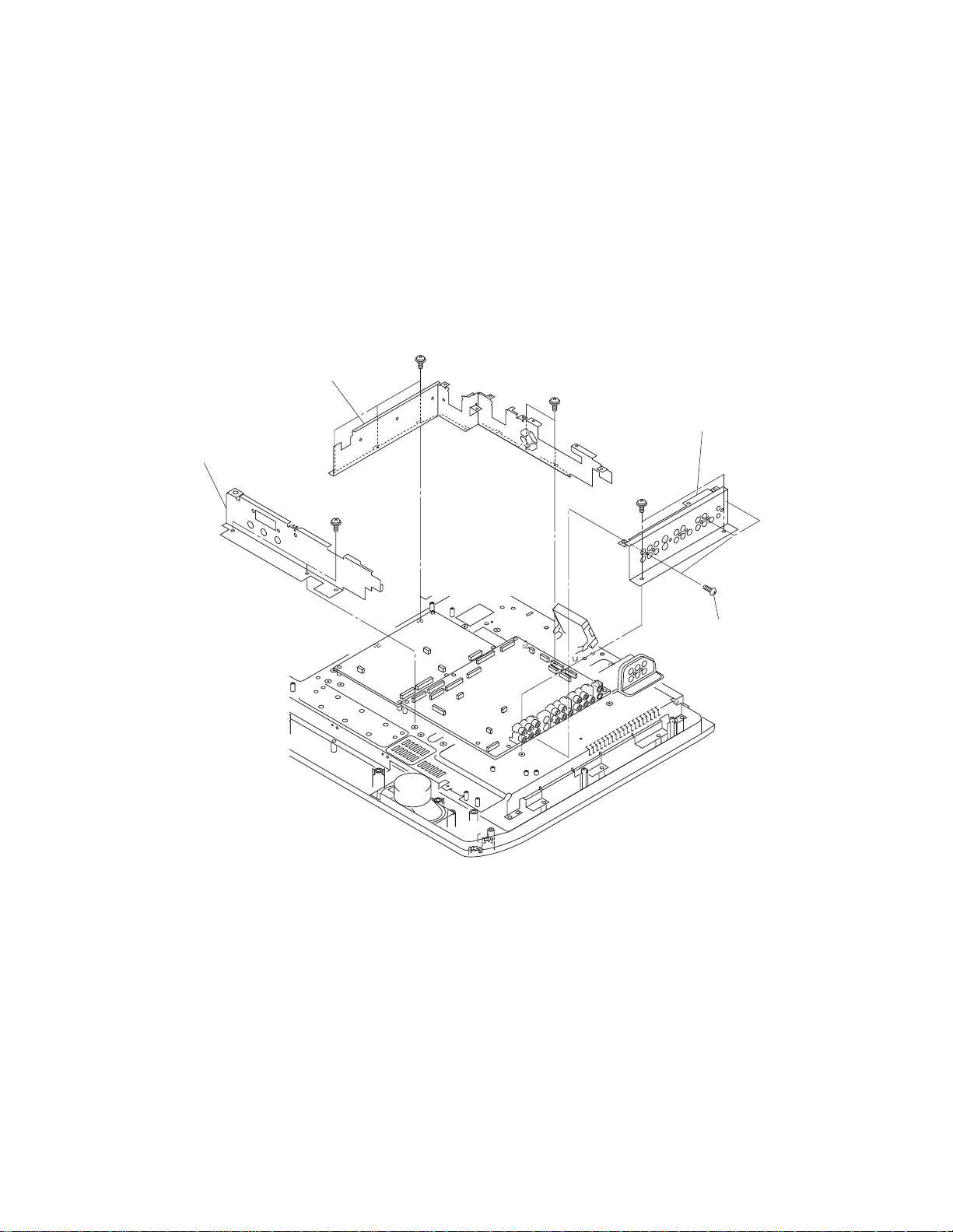
8. Removing the TN/AOUT, AV2 and Signal boards
Z
1) Remove the back cover. (Refer to Item 1.)
2) Remove the top shield bracket. (Refer to Item 3.)
3) Remove the Scaler board. (Refer to Item 5.)
4) Remove the D-Rewrite board. (Refer to Item 6.)
5) Remove the back plates. (Refer to Item 7.)
6) Remove the connector [A] and 3 harnesses from the TN/AOUT board.
7) Remove 5 screws (STP 3x8), then remove the TN/AOUT board.
8) Remove the connector [B] from the Signal board.
9) Remove 3 screws (STP 3x8), then remove the AV2 board.
10) Remove 1 screw (BIDT2 3x10BZ), then remove the AV2 panel.
11) Remove the 6 wire harnesses and 2 FFC from the Signal board.
12) Remove 5 screws (STP 3x8), then remove the Signal board.
TN/AOUT board
Connector [A]
Wire harnesses
STP 3x8
Wire harness
Wire harness
FFC
FFC
Connector [B]
STP 3x8
AV2
board
STP 3x8
Wire harness
SIGNAL
board
BIDT2 3x10 B
AV2 panel
SIGNAL board
– 21 –
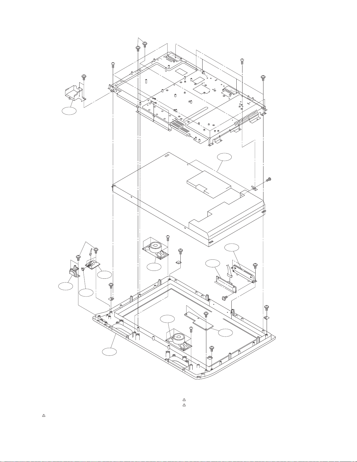
9. Removing the Front /AV board
1) Remove the back cover. (Refer to Item 1.)
2) Remove 1 screw (BIDT2 3x10 BZ).
3) Remove 2 screws (PP 3x6), then remove the front AV panel.
4) Remove 1 screw (BIDT2 3x10 BZ) and 1 screw (PP 3x6), then remove the rear AV panel.
5) Disconnect the 2 wire harnesses and 1 FFC from the Front/AV board.
6) Remove 2 screws (PP 3x6), then remove the wire holder and Front/AV board.
Wire harnesses
PP 3x6
Wire holder
FFC
PP 3x6
Rear AV panel
FRONT/AV board
PP 3x6
Front AV panel
BIDT2 3x10 BZ
– 22 –
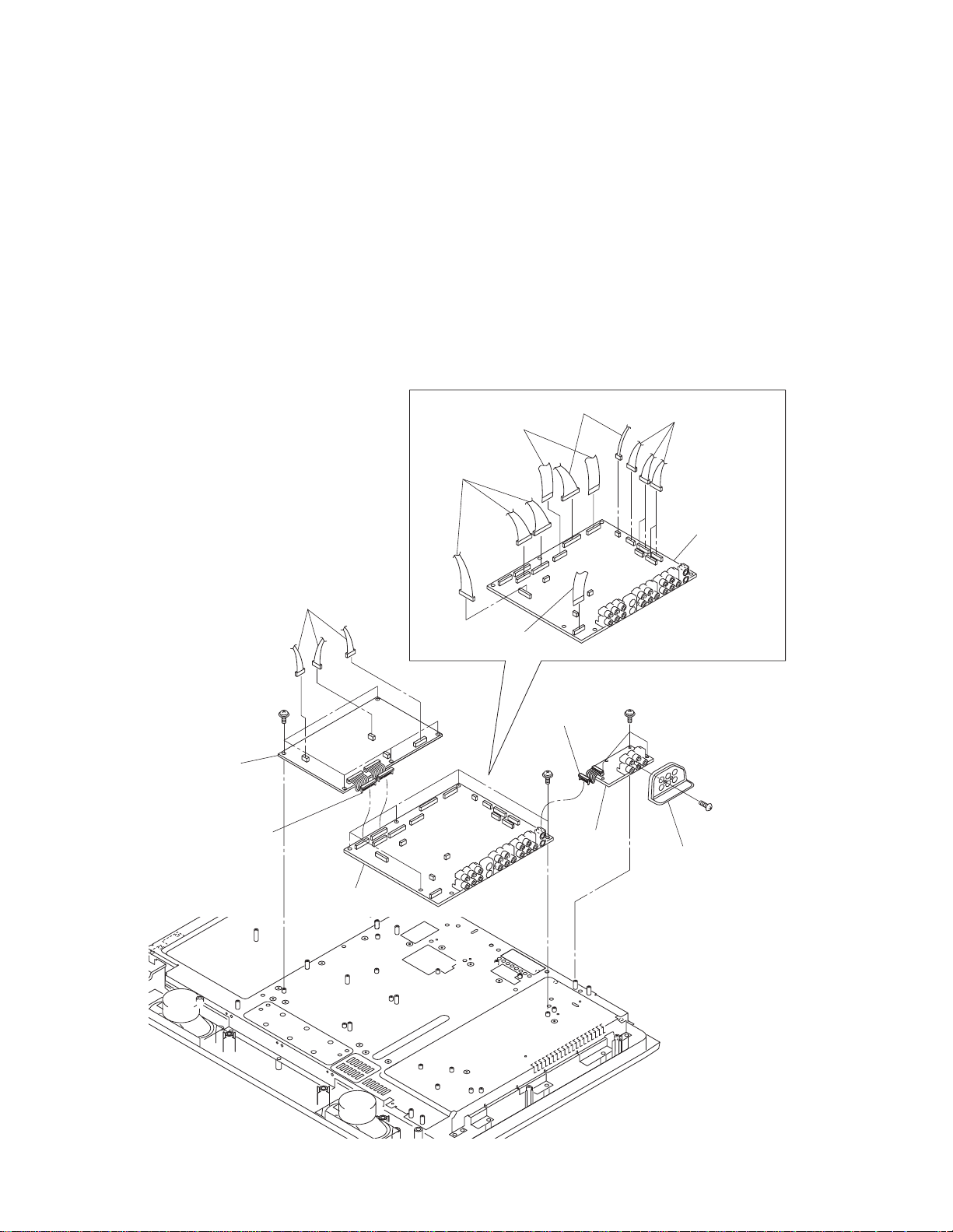
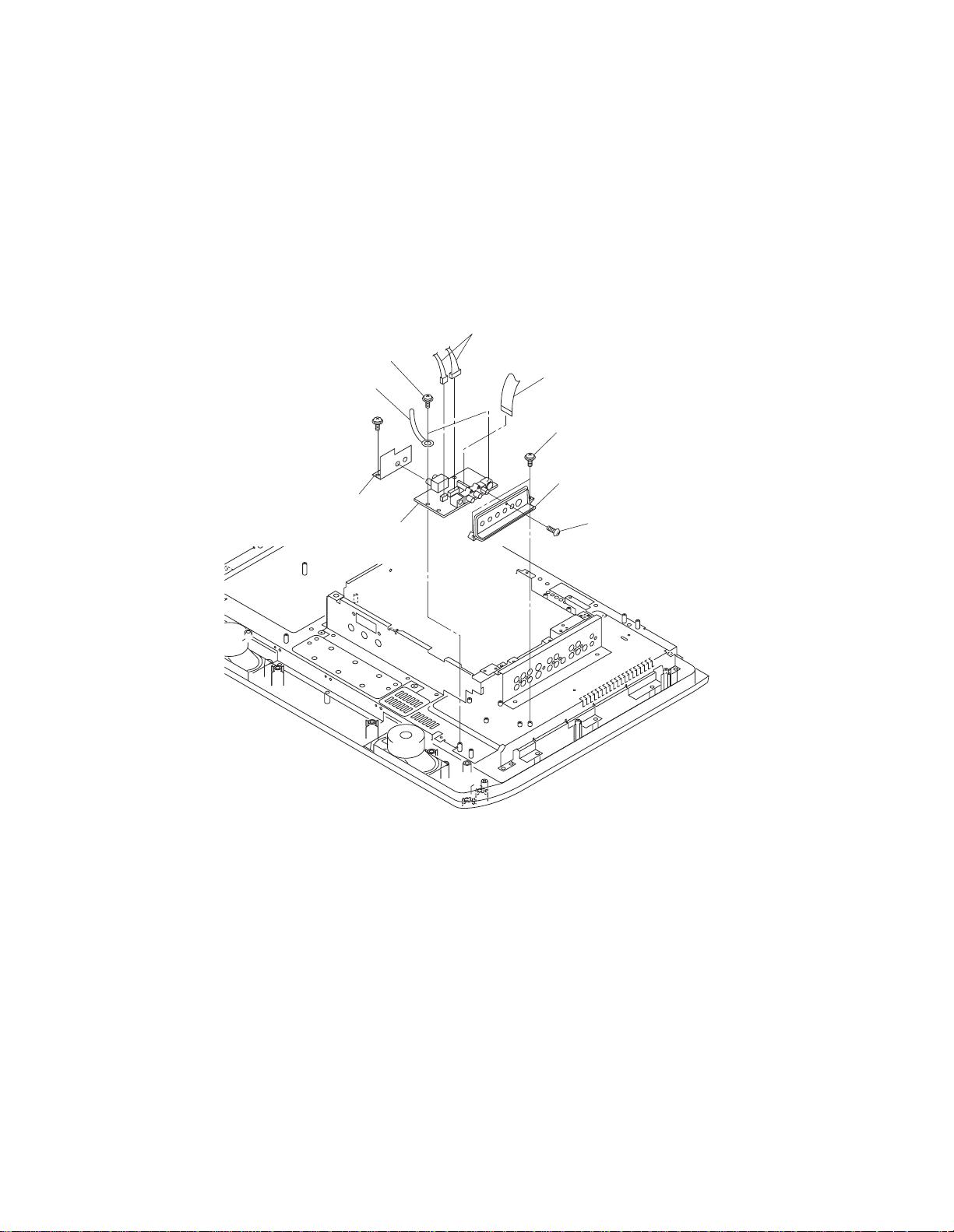
10. Removing the Power SW and LED/RMT boards
1) Remove the back cover. (Refer to Item 1.)
2) Remove 3 screws (STP 3x8), then remove the LED/RMT board.
3) Disconnect the 2 wire harnesses from the connector on the LED/RMT board.
4) Remove 2 screws (STP 3x8), then remove the switch cover and cap.
5) Disconnect the wire harness from the connector on the Power SW board.
6) Remove 3 screws (STP 3x8), then remove the Power SW board.
Wire harness
STP 3x8
STP 3x8
POWER SW
board
Switch cover
Cap
STP 3x8
LED/RMT board
Wire harnesses
– 23 –
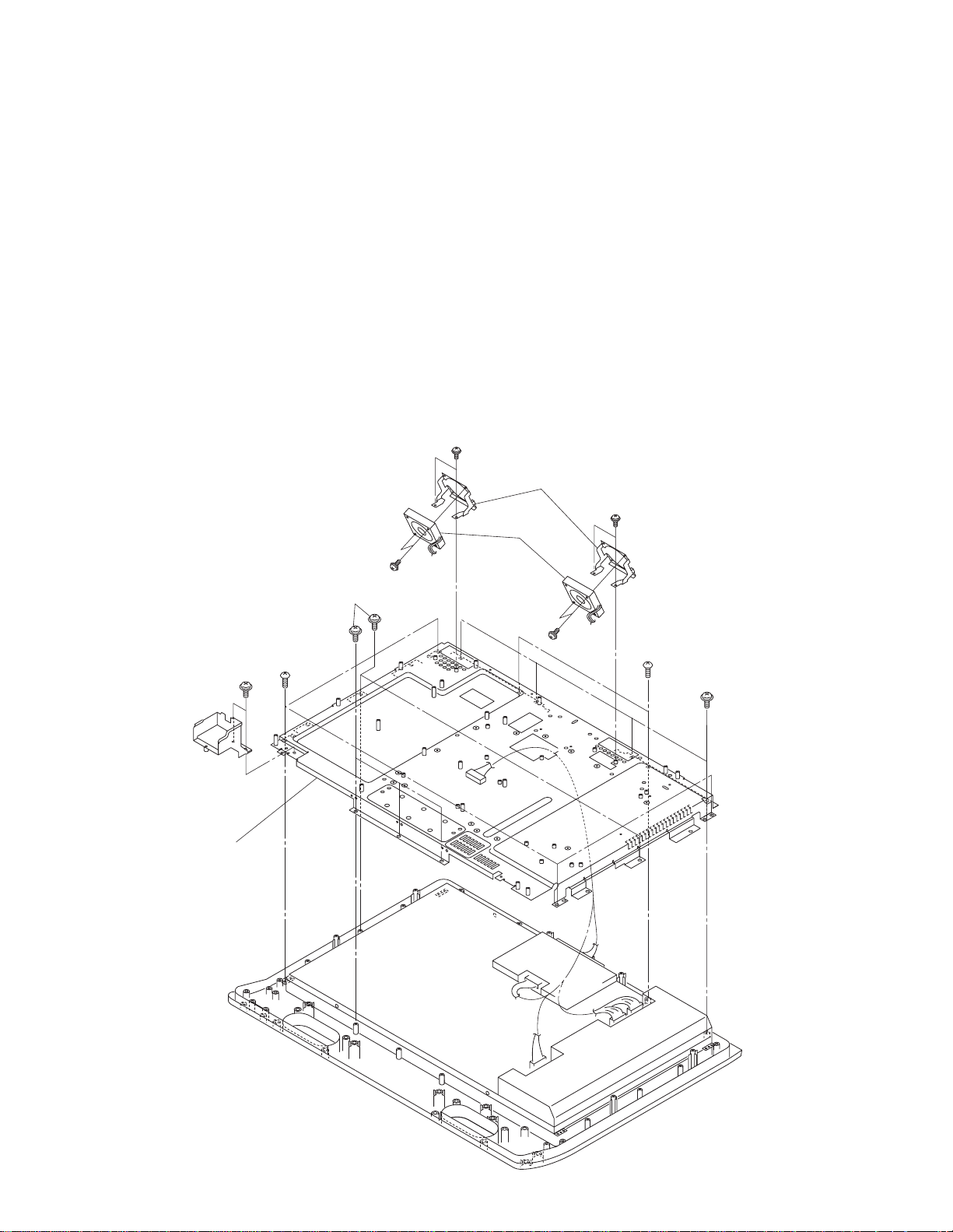
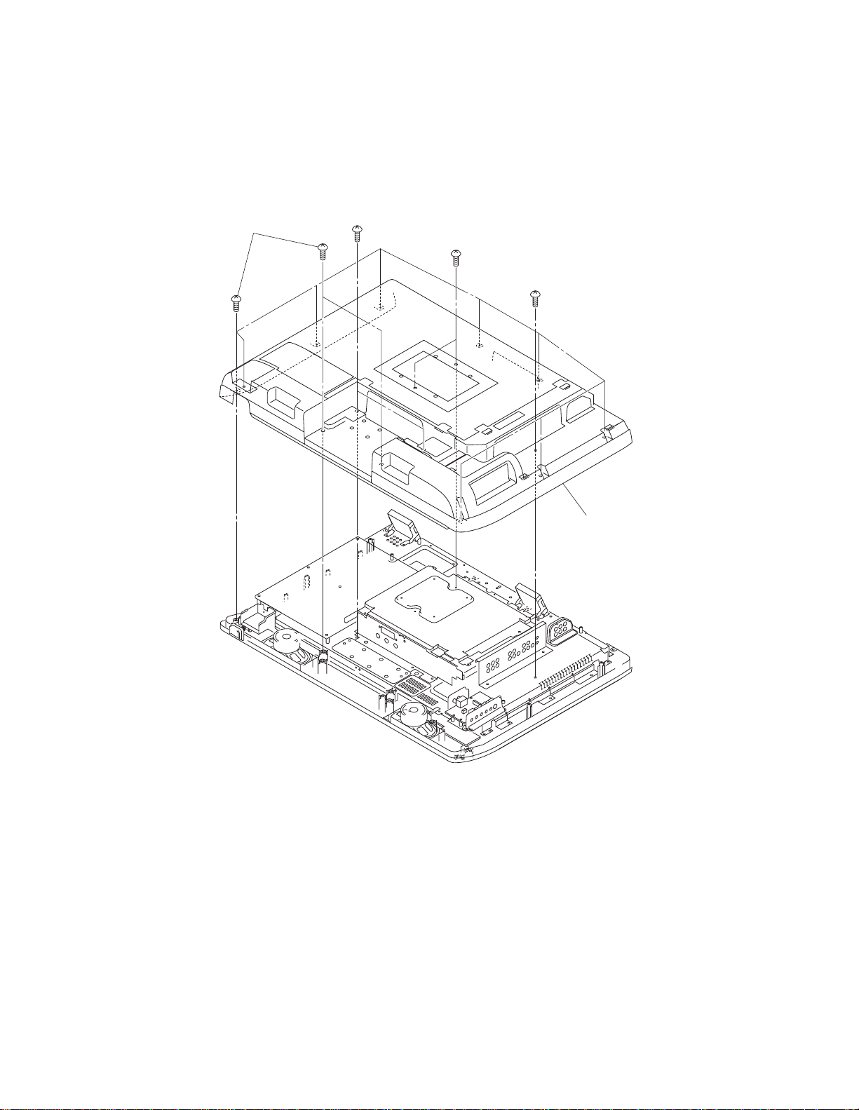
11. Removing the chassis frame
1) Remove the back cover. (Refer to Item 1.)
2) Remove the speakers. (Refer to Item 2.)
3) Remove the top shield bracket. (Refer to Item 3.)
4) Remove Power Module unit. (Refer to Item 4.)
5) Remove the Scaler board. (Refer to Item 5.)
6) Remove the D-Rewrite board and bracket. (Refer to Item 6.)
7) Remove the back plate. (Refer to Item 7.)
8) Remove the TU/AOUT, AV2 and Signal boards. (Refer to Item 8.)
9) Remove the Front/AV board. (Refer to Item 9.)
10) Remove the Power SW and LED/RMT boards. (Refer to Item 10.)
11) Remove 2 screws (PP 3x6), then remove the cord holder.
12) Remove 4 screws (PP 3x6), then remove 2 fan bracket holders.
13) Remove 4 screws (PP 3x20), then remove the 2 DC fans.
14) Remove 10 screws (PBI 4x12) and 8screws (PP 4x10), then remove the chassis frame.
PP 3x6
Fan bracket holder
PP 3x6
DC Fan
PP 3x6
Chassis frame
PP 4x10
PP 3x20
PBI 4x12
PP 3x20
PP 4x10
PBI 4x12
– 24 –
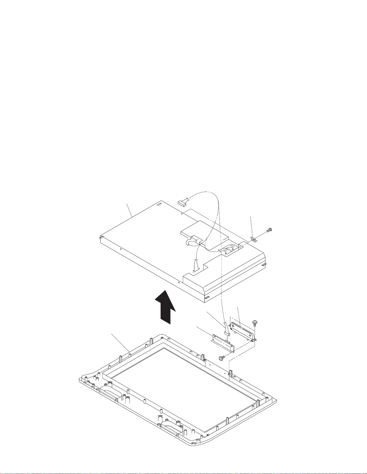
12. Removing the LCD and front bezel cover assembly
1) Remove the back cover. (Refer to Item 1.)
2) Remove the speakers. (Refer to Item 2.)
3) Remove the top shield bracket. (Refer to Item 3.)
4) Remove Power Module unit. (Refer to Item 4.)
5) Remove the Scaler board. (Refer to Item 5.)
6) Remove the D-Rewrite board and bracket. (Refer to Item 6.)
7) Remove the back plate. (Refer to Item 7.)
8) Remove the TU/AOUT,AV2 and Signal boards. (Refer to Item 8.)
9) Remove the Front/AV board. (Refer to Item 9.)
10) Remove the Power SW and LED/RMT boards. (Refer to Item 10.)
11) Remove the chassis frame. (Refer to Item 11.)
12) Remove 2 screws (BIDT2 3x10), then remove the key SW panel.
13) Remove 2 screws (BIDT2 3x10), then remove the Key SW board.
14) Disconnect the wire harness from the connector on the Key SW board.
15) Lift up the LCD slowly from the front bezel cover assembly toward to the arrow direction.
16) Remove 2 screws (PP 4x10), then remove the two bracket panels top.
LCD
Bracket panel top
Front bezel cover assembly
Harness
KEY SW board
BIDT2
3x10
PP 4x10
KEY SW panel
BIDT2 3x10
– 25 –
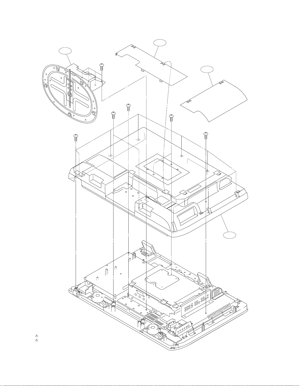
1. Cover Block
A227
EXPLODED VIEWS
A402
PP 5x12
A406
PP 3x8
PBI 4x12
PP 3x8
PBI 4x12
PP 3x8
A401
LOCATION No. Parts No. Description
A227 23429049 CABINET, STAND
A401 23532669 COVER, BACK COVER
A402 23532633 COVER, BC STAND COVER
A406 23532634 COVER, BC TERMINAL COVER
A501 23717176 SCREW, PP5X12+SW+W SZ
A502 23717175 SCREW, PP3X6+SW+W SZ
A505 23035004 SCREW
– 26 –
2. Chassis Block 1
ZA04
A218
PP 3x6
PP 3x6
PP 3x6
P801
PP 3x6
ZA04
ZA01
MJ18
UF01
PP 3x20
MJ94
STP 3x8
MJ13
STP 3x8
STP 3x8
U903
PP 3x6
A218
U800
PP 3x6
A221
U901B
LOCATION No. Parts No. Description
U901B 75000781 PCB PW UNIT FRONT-AV
*
U903 75000789 PCB SCALER
*
A218 23528373 HOLDER, FAN BRACKET 26
A221 23940037 PIECE, REAR AV ASSY
A222 23940038 PIECE, FRONT AV ASSY
MJ13 23389210 FFC CABLE, P0.5-40P
MJ18 23368868 CABLE, LVDS 300MM
MJ94 23389212 FFC CABLE P1.0-11P
MV23
PP 3x6
BIDT2 3x10 BZ
A222
UF01
PP 3x20
LOCATION No. Parts No. Description
MV23 23389213 FFC CABLE, P1.0-19P
P801 23372264 POWER CORD, U/C 125V10A HSV 5
U800 23122467 UNIT, POWER BLOCK MODULE 1H198W
*
UF01 23125908 FAN, DC 12V 60MM, D06R-12SL
ZA01 23103778 FERRITE CORE, TFE1008
ZA04 23103914 FERRITE CORE, TFE1015AD
A502 23717175 SCREW, PP3X6+SW+W SZ
A503 72471064 SCREW, BIDT2 3*10BZ
– 27 –
3. Chassis Block 2
STP 3x8
STP 3x8
STP 3x8
A
H003A
BIDT2
3 x10 BZ
PP 3x6
H003
STP 3x8
STP 3x8
E003
U901G
B
U902
A
STP 3x8
MJ15
B
U901A
STP
3x8
STP
3x8
STP 3x8
BIDT2
3x10 BZ
U901C
A224
BIDT2
3x10 BZ
LOCATION No. Parts No. Description
U901A 75000780 PCB PW UNIT SIGNAL
*
U901C 75000782 PCB PW UNIT AV-2
*
U901G 75000786 PCB PW UNIT D-REWRITE
*
U902 75000787 PCB PW UNIT TN/A-OUT
*
A224 23940036 PIECE, TOP AV ASSY
E003 23148090 MODULE, 03DVI PD0647C
H003 23124083 ANTENNA SWITCH, 2I3O DW US
H003A 23740989 NUT, F-CONNECTOR 2H BS
MJ15 23389211 FFC CABLE, P1.0-25P
A502 23717175 SCREW, PP3X6+SW+W SZ
A503 72471064 SCREW, BIDT2 3*10BZ
A505 23035004 SCREW
– 28 –
4. LCD and Front Bezel Block
PBI 4x12
A219
PP 3x6
PP 4x10
PP 4x10
PBI 4x12
B001
PP 4x10
BIDT2
3x10
U901D
A201
BIDT2
3x10
A203
A215
LOCATION No. Parts No. Description
U901D 75000783 PCB PW UNIT POWER-SW 32HL84
*
U901E 75000784 PCB PW UNIT KEY 32HL84
*
U901F 75000785 PCB PW UNIT IR/LED 32HL84
*
A201 23532746 COVER, FRONT BEZEL ASSY
A202 23940056 PIECE, PIECE KEY ASSY
A203 23940025 PIECE, PIECE POWER ASSY
A215 23940043 PIECE, CAP P SWITCH
W661
PBI 4x12
W661
BIDT2
3x10
U901F
BIDT2
3x10
A202
BIDT2
3x10
BIDT2
3x10
BIDT2
3x10
U901E
BIDT2
PBI
4x12
LOCATION No. Parts No. Description
A219 23528374 HOLDER, HOLDER P CORD JPN
B001 23301561 LCD PANEL, 03SHARP26, LQ255T3LZ11
W661 23351156 SPEAKER, SPK1410AM, 60X120 8-OHM 10W
A502 23717175 SCREW, PP3X6+SW+W SZ
A503 72471064 SCREW, BIDT2 3*10BZ
A504 23738071 SCREW, STP4X10+SW+W SZ
A505 23035004 SCREW
3x10
– 29 –
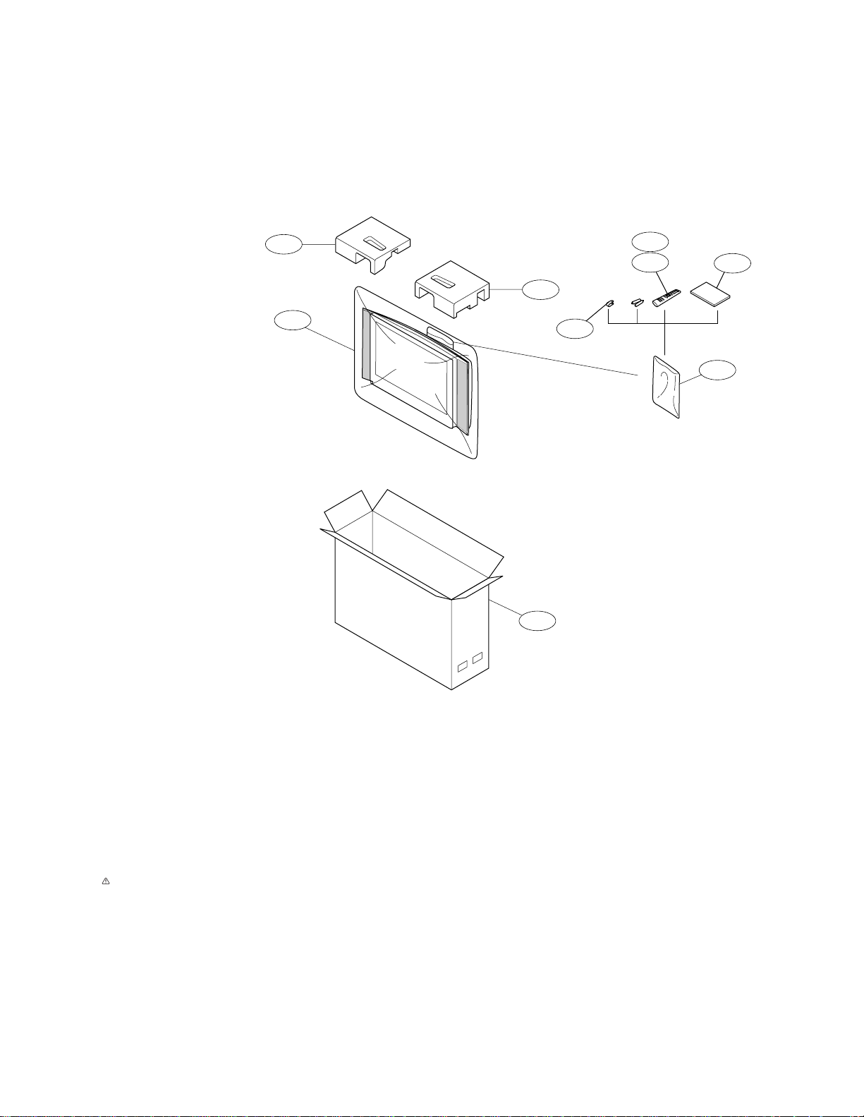
PACKING DISASSEMBLY
A702A
A703
A702A
A701A
Y170
K902
K903
Y101
Y109
LOCATION No. Parts No. Description
A701A 23067704 CARTON, CASE 26HL84
A702A 23946777 PACKING, TOP PACKING 26HL84
A702B 23946778 PACKING, BOTTOM PACKING 26HL84
A703 23945143 BAG, PROTECTIVE, 35P2700
K902 23306504 REMOCON HAND UNIT IR, CTVUSA
K903 23306465 REMOCON HAND UNIT, 57HX82
Y101 23566307 OWNERS MANUAL, ENG/FRE/SPA
Y109 23945015 BAG, POLYETHYLENE COVER, 250X400
Y170 23845800 WIRE HOLDER, NYLON66 D6.8
– 30 –

CHASSIS AND CABINET REPLACEMENT PARTS LIST
WARNING: BEFORE SERVICING THIS CHASSIS, READ THE "X-RAY RADIATION PRECAUTION", "SAFETY PRE-
CAUTION" AND "PRODUCT SAFETY NOTICE" ON PAGE 3 OF THIS MANUAL.
CAUTION: The international hazard symbols " " in the schematic diagram and the parts list designate components
which have special characteristics important for safety and should be replaced only with types identical to those in the
original circuit or specified in the parts list. The mounting position of replacements is to be identical with originals.
Before replacing any of these components, read carefully the PRODUCT SAFETY NOTICE. Do not degrade the safety
of the receiver through improper servicing.
NOTICE:
··
·
The part number must be used when ordering parts, in order to assist in processing, be sure to include the
··
Model number and Description.
··
·
The PC board assembly with * mark is no longer available after the end of the production.
··
Model : 26HL84
Capacitors ............. CD : Ceramic Disk PF : Plastic Film EL : Electrolytic
Resistors ............... CF : Carbon Film CC : Carbon Composition MF : Metal Film
OMF : Oxide Metal Film VR : Variable Resistor FR : Fusible Resistor
(All CD and PF capacitors are
±5%, 50V and all resistors, ±5%, 1/6W unless otherwise noted.)
Location Parts No. Description
No.
CAPACITORS
C102 24793221 ELECTROLYTIC, 10V 220UF M
C103 24109102 CERAMIC CHIP, 50V B 1000PF K
C104 24797479 ELECTROLYTIC, 50V 4.7UF M
C105 24763221 ELECTROLYTIC, 16V 220UF M
C108 24617009 ELECTROLYTIC, 10V 330UF M
C122 24092730 CERAMIC CHIP, 16V B 0.1UF K
C124 24109471 CERAMIC CHIP, 50V B 470PF K
C126 24109471 CERAMIC CHIP, 50V B 470PF K
C127 24763471 ELECTROLYTIC, 16V 470UF M
C131 24793221 ELECTROLYTIC, 10V 220UF M
C132 24763101 ELECTROLYTIC, 16V 100UF M
C133 24109102 CERAMIC CHIP, 50V B 1000PF K
C162 24109472 CERAMIC CHIP, 50V B 4700PF K
C172 24669339 ELECTROLYTIC, 50V 3.3UF M
C522 24100104 CERAMIC CHIP, 25V F 0.1UF Z
C523 24100104 CERAMIC CHIP, 25V F 0.1UF Z
C524 24100104 CERAMIC CHIP, 25V F 0.1UF Z
C601 24092730 CERAMIC CHIP, 16V B 0.1UF K
C602 24109331 CERAMIC CHIP, 50V B 330PF K
C603 24092730 CERAMIC CHIP, 16V B 0.1UF K
C604 24092611 CERAMIC CHIP, 6.3V B 2.2UF K
C605 24109102 CERAMIC CHIP, 50V B 1000PF K
C606 24109102 CERAMIC CHIP, 50V B 1000PF K
C608 24092730 CERAMIC CHIP, 16V B 0.1UF K
C610 24092731 CERAMIC CHIP, 16V B 1UF K
C611 24092730 CERAMIC CHIP, 16V B 0.1UF K
C612 24761102 ELECTROLYTIC CE04G, 6.3V 1000UF M
C613 24092731 CERAMIC CHIP, 16V B 1UF K
C614 24092730 CERAMIC CHIP, 16V B 0.1UF K
C615 24203101 ELECTROLYTIC, 16V 100UF M 7L 3A
C620 24092463 CERAMIC CHIP, 16V B 0.22UF K
C621 24092730 CERAMIC CHIP, 16V B 0.1UF K
C622 24092463 CERAMIC CHIP, 16V B 0.22UF K
C623 24092463 CERAMIC CHIP, 16V B 0.22UF K
C624 24092730 CERAMIC CHIP, 16V B 0.1UF K
C625 24092463 CERAMIC CHIP, 16V B 0.22UF K
C627 24092730 CERAMIC CHIP, 16V B 0.1UF K
C629 24206010 ELECTROLYTIC, 50V 1.0UF M 7L 3A
C630 24092730 CERAMIC CHIP, 16V B 0.1UF K
C631 24092463 CERAMIC CHIP, 16V B 0.22UF K
C632 24092463 CERAMIC CHIP, 16V B 0.22UF K
C635 24763221 ELECTROLYTIC, 16V 220UF M
C636 24763221 ELECTROLYTIC, 16V 220UF M
C640 24762102 ELECTROLYTIC, 04G 10V 1000UF M
C641 24203470 ELECTROLYTIC, 16V 47UF M 7L 3A
Location Parts No. Description
No.
C642 24203470 ELECTROLYTIC, 16V 47UF M 7L 3A
C645 24815103 CERAMIC CHIP, 50V B 10000PF K
C646 24092738 CERAMIC CHIP, 25V B 0.47UF K
C647 24092738 CERAMIC CHIP, 25V B 0.47UF K
C648 24285104 CERAMIC CHIP, 50V B 0.1UF K
C649 24285104 CERAMIC CHIP, 50V B 0.1UF K
C653 24206010 ELECTROLYTIC, 50V 1.0UF M 7L 3A
C661 24109102 CERAMIC CHIP, 50V B 1000PF K
C662 24109102 CERAMIC CHIP, 50V B 1000PF K
C663 24206108 ELECTROLYTIC 04W, 50V 0.1UF M 7L 3A
C665 24206100 ELECTROLYTIC, 50V 10UF M 7L 3A
C666 24206100 ELECTROLYTIC, 50V 10UF M 7L 3A
C667 24092538 CERAMIC CHIP, 10V F 1UF Z
C668 24092538 CERAMIC CHIP, 10V F 1UF Z
C669 24105221 CERAMIC CHIP, 50V CH 220PF J
C672 24092726 CERAMIC CHIP CK733B 16V 2,200,000PFK
C673 24092726 CERAMIC CHIP CK733B 16V 2,200,000PFK
C677 24109391 CERAMIC CHIP CK73B 50V 390PF K
C678 24109391 CERAMIC CHIP CK73B 50V 390PF K
C679 24105221 CERAMIC CHIP, 50V CH 220PF J
C687 24590152 PLASTIC FILM, 50V 1500PF J
C688 24590152 PLASTIC FILM, 50V 1500PF J
C691 24109103 CERAMIC CHIP, 50V B 0.01UF K
C692 24109103 CERAMIC CHIP, 50V B 0.01UF K
C693 24109103 CERAMIC CHIP, 50V B 0.01UF K
C694 24109103 CERAMIC CHIP, 50V B 0.01UF K
C927 24092730 CERAMIC CHIP, 16V B 0.1UF K
CB01 24794470 ELECTROLYTIC, 16V 47UF M
CB40 24092538 CERAMIC CHIP, 10V F 1UF Z
CB41 24109222 CERAMIC CHIP, 50V B 2200PF K
CB42 24105561 CERAMIC CHIP, 50V CH 560PF J
CB43 24109332 CERAMIC CHIP, 50V B 3300PF K
CB45 24092538 CERAMIC CHIP, 10V F 1UF Z
CB46 24109222 CERAMIC CHIP, 50V B 2200PF K
CB47 24105561 CERAMIC CHIP, 50V CH 560PF J
CB51 24590103 PLASTIC FILM, 50V 0.01UF J
CB52 24794470 ELECTROLYTIC, 16V 47UF M
CB53 24503041 PLASTIC FILM , 63V 0.1UF J
CB54 24109221 CERAMIC CHIP, 50V B 220PF K
CB55 24797010 ELECTROLYTIC, 50V 1UF M
CB56 24794470 ELECTROLYTIC, 16V 47UF M
CB57 24503041 PLASTIC FILM , 63V 0.1UF J
CB58 24794470 ELECTROLYTIC, 16V 47UF M
CB59 24590103 PLASTIC FILM, 50V 0.01UF J
CB60 24794100 ELECTROLYTIC, 16V 10UF M
CB61 24503041 PLASTIC FILM , 63V 0.1UF J
– 31 –

Location Parts No. Description
No.
CC01 24109102 CERAMIC CHIP, 50V B 1000PF K
CC02 24109102 CERAMIC CHIP, 50V B 1000PF K
CC03 24109102 CERAMIC CHIP, 50V B 1000PF K
CC04 24109102 CERAMIC CHIP, 50V B 1000PF K
CC05 24109102 CERAMIC CHIP, 50V B 1000PF K
CC06 24109102 CERAMIC CHIP, 50V B 1000PF K
CC07 24109102 CERAMIC CHIP, 50V B 1000PF K
CC08 24109102 CERAMIC CHIP, 50V B 1000PF K
CC09 24109102 CERAMIC CHIP, 50V B 1000PF K
CC10 24109102 CERAMIC CHIP, 50V B 1000PF K
CC11 24109102 CERAMIC CHIP, 50V B 1000PF K
CC12 24109102 CERAMIC CHIP, 50V B 1000PF K
CC14 24109102 CERAMIC CHIP, 50V B 1000PF K
CC15 24109102 CERAMIC CHIP, 50V B 1000PF K
CC18 24109102 CERAMIC CHIP, 50V B 1000PF K
CC19 24109102 CERAMIC CHIP, 50V B 1000PF K
CC77 24105101 CERAMIC CHIP, 50V CH 100PF J
CC78 24105101 CERAMIC CHIP, 50V CH 100PF J
CC99 24591102 PLASTIC FILM, 50V 1000PF J
CD101 24092609 CERAMIC CHIP, 10V B 4,7UF K
CD102 24105271 CERAMIC CHIP, 50V CH 270PF J
CD103 24105101 CERAMIC CHIP, 50V CH 100PF J
CD104 24092609 CERAMIC CHIP, 10V B 4,7UF K
CD105 24105271 CERAMIC CHIP, 50V CH 270PF J
CD106 24105101 CERAMIC CHIP, 50V CH 100PF J
CD107 24092726 CERAMIC CHIP CK733B 16V 2,200,000PFK
CD111 24092609 CERAMIC CHIP, 10V B 4,7UF K
CD112 24105561 CERAMIC CHIP, 50V CH 560PF J
CD113 24105101 CERAMIC CHIP, 50V CH 100PF J
CD114 24092726 CERAMIC CHIP CK733B 16V 2,200,000PFK
CD115 24092609 CERAMIC CHIP, 10V B 4,7UF K
CD116 24105561 CERAMIC CHIP, 50V CH 560PF J
CD117 24105101 CERAMIC CHIP, 50V CH 100PF J
CD118 24092609 CERAMIC CHIP, 10V B 4,7UF K
CD119 24092609 CERAMIC CHIP, 10V B 4,7UF K
CD120 24092542 CERAMIC CHIP CK733 B 16V 1.0UF K
CD121 24100104 CERAMIC CHIP, 25V F 0.1UF Z
CD122 24100104 CERAMIC CHIP, 25V F 0.1UF Z
CD123 24100104 CERAMIC CHIP, 25V F 0.1UF Z
CD124 24100104 CERAMIC CHIP, 25V F 0.1UF Z
CD201 24100104 CERAMIC CHIP, 25V F 0.1UF Z
CD202 24092609 CERAMIC CHIP, 10V B 4,7UF K
CD203 24092609 CERAMIC CHIP, 10V B 4,7UF K
CD204 24109471 CERAMIC CHIP, 50V B 470PF K
CD205 24109471 CERAMIC CHIP, 50V B 470PF K
CD206 24092628 CERAMIC CHIP, 0J B 10UF K
CD207 24100104 CERAMIC CHIP, 25V F 0.1UF Z
CD208 24100104 CERAMIC CHIP, 25V F 0.1UF Z
CD209 24793470 ELECTROLYTIC CE04G 10V 47UF M
CD210 24794470 ELECTROLYTIC, 16V 47UF M
CD211 24100104 CERAMIC CHIP, 25V F 0.1UF Z
CD212 24100104 CERAMIC CHIP, 25V F 0.1UF Z
CD213 24793470 ELECTROLYTIC CE04G 10V 47UF M
CD214 24793470 ELECTROLYTIC CE04G 10V 47UF M
CD215 24100104 CERAMIC CHIP, 25V F 0.1UF Z
CD216 24109102 CERAMIC CHIP, 50V B 1000PF K
CD217 24105270 CERAMIC CHIP, 50V CH 27PF J
CD218 24105100 CERAMIC CHIP, 50V CH 10PF D
CD219 24100104 CERAMIC CHIP, 25V F 0.1UF Z
CD220 24100104 CERAMIC CHIP, 25V F 0.1UF Z
CD221 24100104 CERAMIC CHIP, 25V F 0.1UF Z
CD222 24100104 CERAMIC CHIP, 25V F 0.1UF Z
CD223 24100104 CERAMIC CHIP, 25V F 0.1UF Z
CD224 24100104 CERAMIC CHIP, 25V F 0.1UF Z
CD225 24793470 ELECTROLYTIC CE04G 10V 47UF M
CD226 24100104 CERAMIC CHIP, 25V F 0.1UF Z
CD227 24100104 CERAMIC CHIP, 25V F 0.1UF Z
CD228 24793470 ELECTROLYTIC CE04G 10V 47UF M
CD230 24109103 CERAMIC CHIP, 50V B 0.01UF K
CD233 24092628 CERAMIC CHIP, 0J B 10UF K
CD234 24092573 CERAMIC CHIP, 16V B 0.47UF K
CD235 24100104 CERAMIC CHIP, 25V F 0.1UF Z
CS01 24092538 CERAMIC CHIP, 10V F 1UF Z
CS02 24092538 CERAMIC CHIP, 10V F 1UF Z
CS03 24092538 CERAMIC CHIP, 10V F 1UF Z
CS04 24092538 CERAMIC CHIP, 10V F 1UF Z
Location Parts No. Description
No.
CS05 24092538 CERAMIC CHIP, 10V F 1UF Z
CS06 24092538 CERAMIC CHIP, 10V F 1UF Z
CS07 24092538 CERAMIC CHIP, 10V F 1UF Z
CS08 24092538 CERAMIC CHIP, 10V F 1UF Z
CS09 24092538 CERAMIC CHIP, 10V F 1UF Z
CS10 24092538 CERAMIC CHIP, 10V F 1UF Z
CS11 24092538 CERAMIC CHIP, 10V F 1UF Z
CS12 24092538 CERAMIC CHIP, 10V F 1UF Z
CS13 24092515 CERAMIC CHIP, 16V F 4.7UF Z
CS14 24092515 CERAMIC CHIP, 16V F 4.7UF Z
CS15 24092726 CERAMIC CHIP CK733B 16V 2,200,000PFK
CS16 24092726 CERAMIC CHIP CK733B 16V 2,200,000PFK
CS20 24092573 CERAMIC CHIP, 16V B 0.47UF K
CS21 24092515 CERAMIC CHIP, 16V F 4.7UF Z
CS22 24092515 CERAMIC CHIP, 16V F 4.7UF Z
CS23 24092538 CERAMIC CHIP, 10V F 1UF Z
CS24 24092538 CERAMIC CHIP, 10V F 1UF Z
CS25 24203101 ELECTROLYTIC, 16V 100UF M 7L 3A
CS26 24092726 CERAMIC CHIP CK733B 16V 2,200,000PFK
CS27 24092726 CERAMIC CHIP CK733B 16V 2,200,000PFK
CS30 24092726 CERAMIC CHIP CK733B 16V 2,200,000PFK
CS31 24092726 CERAMIC CHIP CK733B 16V 2,200,000PFK
CS34 24092731 CERAMIC CHIP, 16V B 1UF K
CS35 24092731 CERAMIC CHIP, 16V B 1UF K
CS39 24092538 CERAMIC CHIP, 10V F 1UF Z
CS51 24092515 CERAMIC CHIP, 16V F 4.7UF Z
CS501 24797100 ELECTROLYTIC, 50V 10UF M
CS502 24092726 CERAMIC CHIP CK733B 16V 2,200,000PFK
CS503 24797100 ELECTROLYTIC, 50V 10UF M
CS510 24092542 CERAMIC CHIP CK733 B 16V 1.0UF K
CV01 24092621 CERAMIC CHIP, 10V B 1UF K
CV02 24092621 CERAMIC CHIP, 10V B 1UF K
CV03 24092621 CERAMIC CHIP, 10V B 1UF K
CV04 24100104 CERAMIC CHIP, 25V F 0.1UF Z
CV05 24092621 CERAMIC CHIP, 10V B 1UF K
CV06 24092621 CERAMIC CHIP, 10V B 1UF K
CV07 24100104 CERAMIC CHIP, 25V F 0.1UF Z
CV08 24203101 ELECTROLYTIC, 16V 100UF M 7L 3A
CV09 24092621 CERAMIC CHIP, 10V B 1UF K
CV10 24203100 ELECTORLYTIC, 16V 10UF M 7L 3A
CV11 24092621 CERAMIC CHIP, 10V B 1UF K
CV12 24100104 CERAMIC CHIP, 25V F 0.1UF Z
CV13 24100104 CERAMIC CHIP, 25V F 0.1UF Z
CV14 24092621 CERAMIC CHIP, 10V B 1UF K
CV15 24100104 CERAMIC CHIP, 25V F 0.1UF Z
CV23 24203101 ELECTROLYTIC, 16V 100UF M 7L 3A
CV24 24100104 CERAMIC CHIP, 25V F 0.1UF Z
CV38 24109102 CERAMIC CHIP, 50V B 1000PF K
CV39 24109102 CERAMIC CHIP, 50V B 1000PF K
CV40 24203101 ELECTROLYTIC, 16V 100UF M 7L 3A
CV42 24100104 CERAMIC CHIP, 25V F 0.1UF Z
CV45 24092621 CERAMIC CHIP, 10V B 1UF K
CV46 24092621 CERAMIC CHIP, 10V B 1UF K
CV47 24092621 CERAMIC CHIP, 10V B 1UF K
CV48 24109332 CERAMIC CHIP, 50V B 3300PF K
CV64 24794471 ELECTROLYTIC, 16V 470UF M
CV65 24203101 ELECTROLYTIC, 16V 100UF M 7L 3A
CV66 24100104 CERAMIC CHIP, 25V F 0.1UF Z
CV67 24085981 ELEC. NONPOLAR CE04J 16V 10UF M 11L NP
CV68 24100104 CERAMIC CHIP, 25V F 0.1UF Z
CV73 24100104 CERAMIC CHIP, 25V F 0.1UF Z
CV79 24763471 ELECTROLYTIC, 16V 470UF M
CV80 24762102 ELECTROLYTIC, 04G 10V 1000UF M
CV81 24763471 ELECTROLYTIC, 16V 470UF M
CV82 24762102 ELECTROLYTIC, 04G 10V 1000UF M
CV121 24109103 CERAMIC CHIP, 50V B 0.01UF K
CV237 24100104 CERAMIC CHIP, 25V F 0.1UF Z
CV238 24109103 CERAMIC CHIP, 50V B 0.01UF K
CV239 24100104 CERAMIC CHIP, 25V F 0.1UF Z
CV243 24203100 ELECTORLYTIC, 16V 10UF M 7L 3A
CV244 24109103 CERAMIC CHIP, 50V B 0.01UF K
CV245 24092441 CERAMIC CHIP, 16V F 1UF Z
CV246 24092441 CERAMIC CHIP, 16V F 1UF Z
CV247 24092441 CERAMIC CHIP, 16V F 1UF Z
CV248 24109103 CERAMIC CHIP, 50V B 0.01UF K
CV249 24092441 CERAMIC CHIP, 16V F 1UF Z
– 32 –

Location Parts No. Description
No.
CV250 24092441 CERAMIC CHIP, 16V F 1UF Z
CV251 24092441 CERAMIC CHIP, 16V F 1UF Z
CV252 24109103 CERAMIC CHIP, 50V B 0.01UF K
CV253 24092441 CERAMIC CHIP, 16V F 1UF Z
CV254 24092441 CERAMIC CHIP, 16V F 1UF Z
CV255 24092441 CERAMIC CHIP, 16V F 1UF Z
CV256 24109103 CERAMIC CHIP, 50V B 0.01UF K
CV257 24203100 ELECTORLYTIC, 16V 10UF M 7L 3A
CV258 24203100 ELECTORLYTIC, 16V 10UF M 7L 3A
CV259 24109103 CERAMIC CHIP, 50V B 0.01UF K
CV261 24109103 CERAMIC CHIP, 50V B 0.01UF K
CV263 24109103 CERAMIC CHIP, 50V B 0.01UF K
CY101 24092441 CERAMIC CHIP, 16V F 1UF Z
CY102 24203101 ELECTROLYTIC, 16V 100UF M 7L 3A
CY103 24100104 CERAMIC CHIP, 25V F 0.1UF Z
CY104 24109103 CERAMIC CHIP, 50V B 0.01UF K
CY105 24109103 CERAMIC CHIP, 50V B 0.01UF K
CY106 24109103 CERAMIC CHIP, 50V B 0.01UF K
CY107 24203100 ELECTORLYTIC, 16V 10UF M 7L 3A
CY108 24100104 CERAMIC CHIP, 25V F 0.1UF Z
CY109 24105101 CERAMIC CHIP, 50V CH 100PF J
CY111 24109103 CERAMIC CHIP, 50V B 0.01UF K
CY112 24105181 CERAMIC CHIP, 50V CH 180PF J
CY113 24109103 CERAMIC CHIP, 50V B 0.01UF K
CY114 24109103 CERAMIC CHIP, 50V B 0.01UF K
CY115 24105390 CERAMIC CHIP, 50V CH 39PF J
CY116 24105470 CERAMIC CHIP, 50V CH 47PF J
CY117 24105180 CERAMIC CHIP, 50V CH 18PF J
CY501 24109103 CERAMIC CHIP, 50V B 0.01UF K
CY502 24092730 CERAMIC CHIP, 16V B 0.1UF K
CY504 24109222 CERAMIC CHIP, 50V B 2200PF K
CY505 24105120 CERAMIC CHIP, 50V CH 12PF J
CY506 24109103 CERAMIC CHIP, 50V B 0.01UF K
CY508 24092730 CERAMIC CHIP, 16V B 0.1UF K
CY512 24092463 CERAMIC CHIP, 16V B 0.22UF K
CY513 24092730 CERAMIC CHIP, 16V B 0.1UF K
CY514 24092730 CERAMIC CHIP, 16V B 0.1UF K
CY515 24092730 CERAMIC CHIP, 16V B 0.1UF K
CY516 24109103 CERAMIC CHIP, 50V B 0.01UF K
CY517 24092731 CERAMIC CHIP, 16V B 1UF K
CY524 24092730 CERAMIC CHIP, 16V B 0.1UF K
CY525 24092730 CERAMIC CHIP, 16V B 0.1UF K
CY526 24092730 CERAMIC CHIP, 16V B 0.1UF K
CY538 24762102 ELECTROLYTIC, 04G 10V 1000UF M
CY539 24763471 ELECTROLYTIC, 16V 470UF M
CY540 24203101 ELECTROLYTIC, 16V 100UF M 7L 3A
CY541 24762471 ELECTROLYTIC, 04G 10V 470UF M
CY582 24105101 CERAMIC CHIP, 50V CH 100PF J
CY650 24591102 PLASTIC FILM, 50V 1000PF J
RESISTORS
R102 24011101 CHIP, METAL FILM, 1/20W 100 OHM J
R103 24011101 CHIP, METAL FILM, 1/20W 100 OHM J
R104 24011101 CHIP, METAL FILM, 1/20W 100 OHM J
R110 24011101 CHIP, METAL FILM, 1/20W 100 OHM J
R120 24011101 CHIP, METAL FILM, 1/20W 100 OHM J
R121 24011101 CHIP, METAL FILM, 1/20W 100 OHM J
R133 24011101 CHIP, METAL FILM, 1/20W 100 OHM J
R134 24011103 CHIP, METAL FILM, 1/20W 10K OHM J
R135 24011273 CHIP, 1/20W 27K OHM J
R150 24011332 CHIP, METAL FILM, 1/20W 3.3K OHM J
R151 24011562 CHIP, METAL FILM, 1/20W 5.6K OHM J
R152 24011103 CHIP, METAL FILM, 1/20W 10K OHM J
R264 24871750 CHIP, 1/8W 75 OHM J
R265 24871750 CHIP, 1/8W 75 OHM J
R266 24871750 CHIP, 1/8W 75 OHM J
R286 24871750 CHIP, 1/8W 75 OHM J
R287 24871750 CHIP, 1/8W 75 OHM J
R288 24871750 CHIP, 1/8W 75 OHM J
R563 24011472 CHIP, METAL FILM, 1/20W 4.7K OHM J
R600 24000665 FUSIBLE, 1/4W 15 OHM J
R601 24554470 OXIDE METAL FILM, 2W 47 OHM J
R604 24000606 CHIP, 1/16W 8.2K OHM F
R609 24011273 CHIP, 1/20W 27K OHM J
R610 24011124 CHIP, 1/20W 120K OHM J
R611 24011102 CHIP, METAL FILM, 1/20W 1K OHM J
Location Parts No. Description
No.
R612 24011273 CHIP, 1/20W 27K OHM J
R613 24011124 CHIP, 1/20W 120K OHM J
R614 24011103 CHIP, METAL FILM, 1/20W 10K OHM J
R615 24011104 CHIP, METAL FILM, 1/20W 100K OHM J
R616 24011332 CHIP, METAL FILM, 1/20W 3.3K OHM J
R618 24011223 CHIP, METAL FILM, 1/20W 22K OHM J
R619 24011473 CHIP, METAL FILM, 1/20W 47K OHM J
R620 24871100 CHIP, 1/8W 10 OHM J
R623 24871100 CHIP, 1/8W 10 OHM J
R630 24011472 CHIP, METAL FILM, 1/20W 4.7K OHM J
R631 24011223 CHIP, METAL FILM, 1/20W 22K OHM J
R640 24011103 CHIP, METAL FILM, 1/20W 10K OHM J
R641 24011103 CHIP, METAL FILM, 1/20W 10K OHM J
R642 24011102 CHIP, METAL FILM, 1/20W 1K OHM J
R645 24011103 CHIP, METAL FILM, 1/20W 10K OHM J
R646 24011103 CHIP, METAL FILM, 1/20W 10K OHM J
R650 24011102 CHIP, METAL FILM, 1/20W 1K OHM J
R652 24011473 CHIP, METAL FILM, 1/20W 47K OHM J
R655 24011222 CHIP, METAL FILM, 1/20W 2.2K OHM J
R660 24011563 CHIP, METAL FILM, 1/20W 56K OHM J
R661 24011104 CHIP, METAL FILM, 1/20W 100K OHM J
R662 24011104 CHIP, METAL FILM, 1/20W 100K OHM J
R667 24011104 CHIP, METAL FILM, 1/20W 100K OHM J
R670 24011472 CHIP, METAL FILM, 1/20W 4.7K OHM J
R671 24011102 CHIP, METAL FILM, 1/20W 1K OHM J
R672 24011472 CHIP, METAL FILM, 1/20W 4.7K OHM J
R673 24011102 CHIP, METAL FILM, 1/20W 1K OHM J
R674 24011563 CHIP, METAL FILM, 1/20W 56K OHM J
R676 24011473 CHIP, METAL FILM, 1/20W 47K OHM J
R677 24011473 CHIP, METAL FILM, 1/20W 47K OHM J
R678 24011222 CHIP, METAL FILM, 1/20W 2.2K OHM J
R679 24011222 CHIP, METAL FILM, 1/20W 2.2K OHM J
R680 24011473 CHIP, METAL FILM, 1/20W 47K OHM J
R681 24011473 CHIP, METAL FILM, 1/20W 47K OHM J
R686 24011473 CHIP, METAL FILM, 1/20W 47K OHM J
R687 24011473 CHIP, METAL FILM, 1/20W 47K OHM J
R688 24871101 CHIP, 1/8W 100 OHM J
R690 24871101 CHIP, 1/8W 100 OHM J
R929 24011102 CHIP, METAL FILM, 1/20W 1K OHM J
RA71 24011273 CHIP, 1/20W 27K OHM J
RA72 24011153 CHIP, METAL FILM, 1/2OW 15K OHM J
RA73 24011822 CHIP, METAL FILM, 1/20W 8.2K OHM J
RA75 24011822 CHIP, METAL FILM, 1/20W 8.2K OHM J
RA76 24011153 CHIP, METAL FILM, 1/2OW 15K OHM J
RA80 24000445 CHIP JUMPER, 1608TYPE
RB01 24011391 CHIP, 1/20W 390 OHM J
RB04 24011473 CHIP, METAL FILM, 1/20W 47K OHM J
RB05 24011102 CHIP, METAL FILM, 1/20W 1K OHM J
RB15 24011471 CHIP, METAL FILM, 1/20W 470 OHM J
RB19 24011470 CHIP, METAL FILM, 1/20W 47 OHM J
RB37 24011331 CHIP, METAL FILM, 1/20W 330 OHM J
RB38 24011105 CHIP, METAL FILM, 1/20W 1M OHM J
RB39 24011123 CHIP, METAL FILM, 1/20W 12K OHM J
RB40 24011392 CHIP, 1/20W 3.9K OHM J
RB41 24011392 CHIP, 1/20W 3.9K OHM J
RB42 24011103 CHIP, METAL FILM, 1/20W 10K OHM J
RB43 24011331 CHIP, METAL FILM, 1/20W 330 OHM J
RB44 24011105 CHIP, METAL FILM, 1/20W 1M OHM J
RB45 24011123 CHIP, METAL FILM, 1/20W 12K OHM J
RB46 24011392 CHIP, 1/20W 3.9K OHM J
RB47 24011392 CHIP, 1/20W 3.9K OHM J
RB48 24011103 CHIP, METAL FILM, 1/20W 10K OHM J
RB51 24011224 CHIP, METAL FILM, 1/20W 220K OHM J
RB52 24011123 CHIP, METAL FILM, 1/20W 12K OHM J
RB53 24011123 CHIP, METAL FILM, 1/20W 12K OHM J
RB54 24011123 CHIP, METAL FILM, 1/20W 12K OHM J
RB55 24011224 CHIP, METAL FILM, 1/20W 220K OHM J
RB56 24011151 CHIP, METAL FILM, 1/20W 150 OHM J
RB57 24011103 CHIP, METAL FILM, 1/20W 10K OHM J
RB58 24011103 CHIP, METAL FILM, 1/20W 10K OHM J
RB59 24011122 CHIP, METAL FILM, 1/20W 1.2K OHM J
RB60 24011224 CHIP, METAL FILM, 1/20W 220K OHM J
RB62 24011272 CHIP, 1/20W 2.7K OHM J
RB63 24011271 CHIP, 1/20W 270 OHM J
RB64 24011102 CHIP, METAL FILM, 1/20W 1K OHM J
RB65 24011221 CHIP, METAL FILM, 1/20W 220 OHM J
– 33 –

Location Parts No. Description
No.
RB66 24011473 CHIP, METAL FILM, 1/20W 47K OHM J
RB67 24011221 CHIP, METAL FILM, 1/20W 220 OHM J
RB69 24011272 CHIP, 1/20W 2.7K OHM J
RB70 24011331 CHIP, METAL FILM, 1/20W 330 OHM J
RB71 24019112 CHIP, METAL FILM, 1/8W 1 OHM F
RB72 24011220 CHIP, METAL FILM, 1/20W 22 OHM J
RB73 24011560 CHIP, METAL FILM, 1/20W 56 OHM J
RB74 24011104 CHIP, METAL FILM, 1/20W 100K OHM J
RC01 24011681 CHIP, METAL FILM, 1/20W 680 OHM J
RC02 24011681 CHIP, METAL FILM, 1/20W 680 OHM J
RC03 24011681 CHIP, METAL FILM, 1/20W 680 OHM J
RC04 24011681 CHIP, METAL FILM, 1/20W 680 OHM J
RC05 24011681 CHIP, METAL FILM, 1/20W 680 OHM J
RC06 24011681 CHIP, METAL FILM, 1/20W 680 OHM J
RC07 24011681 CHIP, METAL FILM, 1/20W 680 OHM J
RC08 24011681 CHIP, METAL FILM, 1/20W 680 OHM J
RC11 24011681 CHIP, METAL FILM, 1/20W 680 OHM J
RC12 24011681 CHIP, METAL FILM, 1/20W 680 OHM J
RC15 24011681 CHIP, METAL FILM, 1/20W 680 OHM J
RC16 24011681 CHIP, METAL FILM, 1/20W 680 OHM J
RD101 24011823 CHIP, METAL FILM, 1/20W 82K OHM J
RD102 24011473 CHIP, METAL FILM, 1/20W 47K OHM J
RD103 24011333 CHIP, METAL FILM, 1/20W 33K OHM J
RD104 24011393 CHIP, 1/20W 39K OHM J
RD105 24011472 CHIP, METAL FILM, 1/20W 4.7K OHM J
RD106 24011823 CHIP, METAL FILM, 1/20W 82K OHM J
RD107 24011473 CHIP, METAL FILM, 1/20W 47K OHM J
RD108 24011333 CHIP, METAL FILM, 1/20W 33K OHM J
RD109 24011393 CHIP, 1/20W 39K OHM J
RD110 24011472 CHIP, METAL FILM, 1/20W 4.7K OHM J
RD111 24011223 CHIP, METAL FILM, 1/20W 22K OHM J
RD112 24011473 CHIP, METAL FILM, 1/20W 47K OHM J
RD113 24011153 CHIP, METAL FILM, 1/2OW 15K OHM J
RD114 24011473 CHIP, METAL FILM, 1/20W 47K OHM J
RD115 24011222 CHIP, METAL FILM, 1/20W 2.2K OHM J
RD116 24011223 CHIP, METAL FILM, 1/20W 22K OHM J
RD117 24011473 CHIP, METAL FILM, 1/20W 47K OHM J
RD118 24011153 CHIP, METAL FILM, 1/2OW 15K OHM J
RD119 24011473 CHIP, METAL FILM, 1/20W 47K OHM J
RD120 24011222 CHIP, METAL FILM, 1/20W 2.2K OHM J
RD130 24011182 CHIP, METAL FILM, 1/20W 1.8K OHM J
RD201 24011101 CHIP, METAL FILM, 1/20W 100 OHM J
RD202 24011103 CHIP, METAL FILM, 1/20W 10K OHM J
RD203 24011101 CHIP, METAL FILM, 1/20W 100 OHM J
RD204 24011101 CHIP, METAL FILM, 1/20W 100 OHM J
RD205 24011103 CHIP, METAL FILM, 1/20W 10K OHM J
RD206 24011101 CHIP, METAL FILM, 1/20W 100 OHM J
RD208 24011472 CHIP, METAL FILM, 1/20W 4.7K OHM J
RD210 24011101 CHIP, METAL FILM, 1/20W 100 OHM J
RD211 24011101 CHIP, METAL FILM, 1/20W 100 OHM J
RD212 24011101 CHIP, METAL FILM, 1/20W 100 OHM J
RD213 24011101 CHIP, METAL FILM, 1/20W 100 OHM J
RD214 24011101 CHIP, METAL FILM, 1/20W 100 OHM J
RD215 24011103 CHIP, METAL FILM, 1/20W 10K OHM J
RD216 24011103 CHIP, METAL FILM, 1/20W 10K OHM J
RD217 24011105 CHIP, METAL FILM, 1/20W 1M OHM J
RD218 24011241 CHIP, METAL FILM, 1/20W 240 OHM J
RD219 24011101 CHIP, METAL FILM, 1/20W 100 OHM J
RD220 24011101 CHIP, METAL FILM, 1/20W 100 OHM J
RD221 24011103 CHIP, METAL FILM, 1/20W 10K OHM J
RD222 24011103 CHIP, METAL FILM, 1/20W 10K OHM J
RD223 24011103 CHIP, METAL FILM, 1/20W 10K OHM J
RD224 24011103 CHIP, METAL FILM, 1/20W 10K OHM J
RD225 24011101 CHIP, METAL FILM, 1/20W 100 OHM J
RD226 24011101 CHIP, METAL FILM, 1/20W 100 OHM J
RD227 24011472 CHIP, METAL FILM, 1/20W 4.7K OHM J
RD228 24011472 CHIP, METAL FILM, 1/20W 4.7K OHM J
RD229 24011101 CHIP, METAL FILM, 1/20W 100 OHM J
RD230 24011102 CHIP, METAL FILM, 1/20W 1K OHM J
RD233 24011102 CHIP, METAL FILM, 1/20W 1K OHM J
RD234 24011332 CHIP, METAL FILM, 1/20W 3.3K OHM J
RD235 24011332 CHIP, METAL FILM, 1/20W 3.3K OHM J
RD236 24011101 CHIP, METAL FILM, 1/20W 100 OHM J
RD237 24011101 CHIP, METAL FILM, 1/20W 100 OHM J
RD238 24011101 CHIP, METAL FILM, 1/20W 100 OHM J
RD239 24011101 CHIP, METAL FILM, 1/20W 100 OHM J
Location Parts No. Description
No.
RD240 24011101 CHIP, METAL FILM, 1/20W 100 OHM J
RD248 24011473 CHIP, METAL FILM, 1/20W 47K OHM J
RD249 24011101 CHIP, METAL FILM, 1/20W 100 OHM J
RD250 24011101 CHIP, METAL FILM, 1/20W 100 OHM J
RD251 24011332 CHIP, METAL FILM, 1/20W 3.3K OHM J
RJ40 24000445 CHIP JUMPER, 1608TYPE
RJ41 24000445 CHIP JUMPER, 1608TYPE
RS01 24011562 CHIP, METAL FILM, 1/20W 5.6K OHM J
RS02 24011562 CHIP, METAL FILM, 1/20W 5.6K OHM J
RS03 24011562 CHIP, METAL FILM, 1/20W 5.6K OHM J
RS04 24011562 CHIP, METAL FILM, 1/20W 5.6K OHM J
RS05 24011562 CHIP, METAL FILM, 1/20W 5.6K OHM J
RS06 24011562 CHIP, METAL FILM, 1/20W 5.6K OHM J
RS07 24011562 CHIP, METAL FILM, 1/20W 5.6K OHM J
RS08 24011562 CHIP, METAL FILM, 1/20W 5.6K OHM J
RS09 24011562 CHIP, METAL FILM, 1/20W 5.6K OHM J
RS10 24011562 CHIP, METAL FILM, 1/20W 5.6K OHM J
RS11 24011101 CHIP, METAL FILM, 1/20W 100 OHM J
RS12 24011101 CHIP, METAL FILM, 1/20W 100 OHM J
RS13 24011472 CHIP, METAL FILM, 1/20W 4.7K OHM J
RS14 24011331 CHIP, METAL FILM, 1/20W 330 OHM J
RS15 24011101 CHIP, METAL FILM, 1/20W 100 OHM J
RS16 24011101 CHIP, METAL FILM, 1/20W 100 OHM J
RS17 24011101 CHIP, METAL FILM, 1/20W 100 OHM J
RS18 24011101 CHIP, METAL FILM, 1/20W 100 OHM J
RS19 24011101 CHIP, METAL FILM, 1/20W 100 OHM J
RS20 24011101 CHIP, METAL FILM, 1/20W 100 OHM J
RS21 24011222 CHIP, METAL FILM, 1/20W 2.2K OHM J
RS22 24011222 CHIP, METAL FILM, 1/20W 2.2K OHM J
RS25 24011101 CHIP, METAL FILM, 1/20W 100 OHM J
RS26 24011101 CHIP, METAL FILM, 1/20W 100 OHM J
RS27 24011102 CHIP, METAL FILM, 1/20W 1K OHM J
RS28 24011102 CHIP, METAL FILM, 1/20W 1K OHM J
RS29 24011102 CHIP, METAL FILM, 1/20W 1K OHM J
RS30 24011102 CHIP, METAL FILM, 1/20W 1K OHM J
RS31 24011104 CHIP, METAL FILM, 1/20W 100K OHM J
RS32 24011104 CHIP, METAL FILM, 1/20W 100K OHM J
RS33 24011473 CHIP, METAL FILM, 1/20W 47K OHM J
RS34 24011473 CHIP, METAL FILM, 1/20W 47K OHM J
RS35 24011104 CHIP, METAL FILM, 1/20W 100K OHM J
RS36 24011472 CHIP, METAL FILM, 1/20W 4.7K OHM J
RS37 24011104 CHIP, METAL FILM, 1/20W 100K OHM J
RS38 24011104 CHIP, METAL FILM, 1/20W 100K OHM J
RS39 24011104 CHIP, METAL FILM, 1/20W 100K OHM J
RS40 24011104 CHIP, METAL FILM, 1/20W 100K OHM J
RS41 24011104 CHIP, METAL FILM, 1/20W 100K OHM J
RS42 24011104 CHIP, METAL FILM, 1/20W 100K OHM J
RS44 24011104 CHIP, METAL FILM, 1/20W 100K OHM J
RS45 24011103 CHIP, METAL FILM, 1/20W 10K OHM J
RS46 24011103 CHIP, METAL FILM, 1/20W 10K OHM J
RS47 24011473 CHIP, METAL FILM, 1/20W 47K OHM J
RS48 24011473 CHIP, METAL FILM, 1/20W 47K OHM J
RS49 24011473 CHIP, METAL FILM, 1/20W 47K OHM J
RS50 24011473 CHIP, METAL FILM, 1/20W 47K OHM J
RS51 24011272 CHIP, 1/20W 2.7K OHM J
RS52 24011182 CHIP, METAL FILM, 1/20W 1.8K OHM J
RS53 24011473 CHIP, METAL FILM, 1/20W 47K OHM J
RS54 24011563 CHIP, METAL FILM, 1/20W 56K OHM J
RS55 24011103 CHIP, METAL FILM, 1/20W 10K OHM J
RS56 24011104 CHIP, METAL FILM, 1/20W 100K OHM J
RS57 24011562 CHIP, METAL FILM, 1/20W 5.6K OHM J
RS58 24011562 CHIP, METAL FILM, 1/20W 5.6K OHM J
RS59 24011562 CHIP, METAL FILM, 1/20W 5.6K OHM J
RS60 24011562 CHIP, METAL FILM, 1/20W 5.6K OHM J
RS61 24011101 CHIP, METAL FILM, 1/20W 100 OHM J
RS62 24011101 CHIP, METAL FILM, 1/20W 100 OHM J
RS63 24011102 CHIP, METAL FILM, 1/20W 1K OHM J
RS64 24011393 CHIP, 1/20W 39K OHM J
RS65 24011563 CHIP, METAL FILM, 1/20W 56K OHM J
RS66 24011393 CHIP, 1/20W 39K OHM J
RS67 24011563 CHIP, METAL FILM, 1/20W 56K OHM J
RS74 24011102 CHIP, METAL FILM, 1/20W 1K OHM J
RS75 24011224 CHIP, METAL FILM, 1/20W 220K OHM J
RS76 24011562 CHIP, METAL FILM, 1/20W 5.6K OHM J
RS79 24011104 CHIP, METAL FILM, 1/20W 100K OHM J
RS80 24011104 CHIP, METAL FILM, 1/20W 100K OHM J
– 34 –

Location Parts No. Description
No.
RS103 24011103 CHIP, METAL FILM, 1/20W 10K OHM J
RS112 24011473 CHIP, METAL FILM, 1/20W 47K OHM J
RS116 24011473 CHIP, METAL FILM, 1/20W 47K OHM J
RS500 24011393 CHIP, 1/20W 39K OHM J
RS501 24011103 CHIP, METAL FILM, 1/20W 10K OHM J
RS504 24011103 CHIP, METAL FILM, 1/20W 10K OHM J
RS505 24011393 CHIP, 1/20W 39K OHM J
RS506 24011472 CHIP, METAL FILM, 1/20W 4.7K OHM J
RS507 24011472 CHIP, METAL FILM, 1/20W 4.7K OHM J
RS515 24011392 CHIP, 1/20W 3.9K OHM J
RS516 24011473 CHIP, METAL FILM, 1/20W 47K OHM J
RS517 24011473 CHIP, METAL FILM, 1/20W 47K OHM J
RT01 24019527
RV01 24011101 CHIP, METAL FILM, 1/20W 100 OHM J
RV03 24011101 CHIP, METAL FILM, 1/20W 100 OHM J
RV06 24011101 CHIP, METAL FILM, 1/20W 100 OHM J
RV07 24011102 CHIP, METAL FILM, 1/20W 1K OHM J
RV08 24011101 CHIP, METAL FILM, 1/20W 100 OHM J
RV09 24011101 CHIP, METAL FILM, 1/20W 100 OHM J
RV10 24011101 CHIP, METAL FILM, 1/20W 100 OHM J
RV11 24011101 CHIP, METAL FILM, 1/20W 100 OHM J
RV12 24011101 CHIP, METAL FILM, 1/20W 100 OHM J
RV14 24011562 CHIP, METAL FILM, 1/20W 5.6K OHM J
RV15 24011101 CHIP, METAL FILM, 1/20W 100 OHM J
RV17 24011101 CHIP, METAL FILM, 1/20W 100 OHM J
RV19 24011101 CHIP, METAL FILM, 1/20W 100 OHM J
RV20 24011101 CHIP, METAL FILM, 1/20W 100 OHM J
RV21 24011101 CHIP, METAL FILM, 1/20W 100 OHM J
RV26 24011561 CHIP, METAL FILM, 1/20W 560 OHM J
RV27 24011101 CHIP, METAL FILM, 1/20W 100 OHM J
RV29 24552101 OXIDE METAL FILM, 1/2W 100 OHM J
RV30 24011101 CHIP, METAL FILM, 1/20W 100 OHM J
RV33 24871750 CHIP, 1/8W 75 OHM J
RV34 24871750 CHIP, 1/8W 75 OHM J
RV35 24871750 CHIP, 1/8W 75 OHM J
RV36 24871750 CHIP, 1/8W 75 OHM J
RV37 24871750 CHIP, 1/8W 75 OHM J
RV40 24871750 CHIP, 1/8W 75 OHM J
RV41 24011101 CHIP, METAL FILM, 1/20W 100 OHM J
RV60 24011222 CHIP, METAL FILM, 1/20W 2.2K OHM J
RV61 24011101 CHIP, METAL FILM, 1/20W 100 OHM J
RV62 24011101 CHIP, METAL FILM, 1/20W 100 OHM J
RV66 24011750 CHIP, METAL FILM, 1/20W 75 OHM J
RV70 24011101 CHIP, METAL FILM, 1/20W 100 OHM J
RV71 24011101 CHIP, METAL FILM, 1/20W 100 OHM J
RV72 24011101 CHIP, METAL FILM, 1/20W 100 OHM J
RV73 24011222 CHIP, METAL FILM, 1/20W 2.2K OHM J
RV74 24011222 CHIP, METAL FILM, 1/20W 2.2K OHM J
RV75 24011222 CHIP, METAL FILM, 1/20W 2.2K OHM J
RV76 24011272 CHIP, 1/20W 2.7K OHM J
RV77 24011101 CHIP, METAL FILM, 1/20W 100 OHM J
RV78 24011101 CHIP, METAL FILM, 1/20W 100 OHM J
RV79 24011272 CHIP, 1/20W 2.7K OHM J
RV87 24000445 CHIP JUMPER, 1608TYPE
RV88 24000445 CHIP JUMPER, 1608TYPE
RV89 24000445 CHIP JUMPER, 1608TYPE
RV90 24000445 CHIP JUMPER, 1608TYPE
RV91 24011101 CHIP, METAL FILM, 1/20W 100 OHM J
RV92 24011102 CHIP, METAL FILM, 1/20W 1K OHM J
RV93 24011470 CHIP, METAL FILM, 1/20W 47 OHM J
RV94 24011222 CHIP, METAL FILM, 1/20W 2.2K OHM J
RV98 24000445 CHIP JUMPER, 1608TYPE
RV99 24000445 CHIP JUMPER, 1608TYPE
RV100 24000445 CHIP JUMPER, 1608TYPE
RV101 24000445 CHIP JUMPER, 1608TYPE
RV120 24871750 CHIP, 1/8W 75 OHM J
RV121 24871750 CHIP, 1/8W 75 OHM J
RV122 24871750 CHIP, 1/8W 75 OHM J
RV129 24011101 CHIP, METAL FILM, 1/20W 100 OHM J
RV252 24011101 CHIP, METAL FILM, 1/20W 100 OHM J
RV253 24011102 CHIP, METAL FILM, 1/20W 1K OHM J
RV254 24011101 CHIP, METAL FILM, 1/20W 100 OHM J
RV255 24871561 CHIP, 1/8W 560 OHM J
RV256 24011102 CHIP, METAL FILM, 1/20W 1K OHM J
RV257 24011101 CHIP, METAL FILM, 1/20W 100 OHM J
RV258 24011102 CHIP, METAL FILM, 1/20W 1K OHM J
THERMISTOR, NTC 1608 SIZE NSM3103F344F3R
Location Parts No. Description
No.
RV259 24011102 CHIP, METAL FILM, 1/20W 1K OHM J
RV260 24011101 CHIP, METAL FILM, 1/20W 100 OHM J
RV261 24871561 CHIP, 1/8W 560 OHM J
RV323 24872101 CHIP, 1/16W 100 OHM J
RV324 24872101 CHIP, 1/16W 100 OHM J
RV325 24872101 CHIP, 1/16W 100 OHM J
RV330 24011101 CHIP, METAL FILM, 1/20W 100 OHM J
RV331 24011101 CHIP, METAL FILM, 1/20W 100 OHM J
RV332 24011101 CHIP, METAL FILM, 1/20W 100 OHM J
RV337 24011101 CHIP, METAL FILM, 1/20W 100 OHM J
RV338 24011101 CHIP, METAL FILM, 1/20W 100 OHM J
RV346 24011101 CHIP, METAL FILM, 1/20W 100 OHM J
RV347 24011101 CHIP, METAL FILM, 1/20W 100 OHM J
RV348 24011101 CHIP, METAL FILM, 1/20W 100 OHM J
RV351 24011330 CHIP, 1/20W 33 OHM J
RV352 24011330 CHIP, 1/20W 33 OHM J
RV353 24011330 CHIP, 1/20W 33 OHM J
RV354 24011330 CHIP, 1/20W 33 OHM J
RV355 24011330 CHIP, 1/20W 33 OHM J
RV356 24011330 CHIP, 1/20W 33 OHM J
RV357 24000445 CHIP JUMPER, 1608TYPE
RV358 24000445 CHIP JUMPER, 1608TYPE
RV359 24000445 CHIP JUMPER, 1608TYPE
RV368 24000445 CHIP JUMPER, 1608TYPE
RV369 24000445 CHIP JUMPER, 1608TYPE
RV370 24000445 CHIP JUMPER, 1608TYPE
RV371 24000445 CHIP JUMPER, 1608TYPE
RV372 24000445 CHIP JUMPER, 1608TYPE
RV373 24000445 CHIP JUMPER, 1608TYPE
RV374 24000445 CHIP JUMPER, 1608TYPE
RV375 24000445 CHIP JUMPER, 1608TYPE
RY101 24011101 CHIP, METAL FILM, 1/20W 100 OHM J
RY102 24011221 CHIP, METAL FILM, 1/20W 220 OHM J
RY103 24011102 CHIP, METAL FILM, 1/20W 1K OHM J
RY104 24011102 CHIP, METAL FILM, 1/20W 1K OHM J
RY105 24011821 CHIP, 1/20W 820 OHM J
RY106 24000445 CHIP JUMPER, 1608TYPE
RY107 24011222 CHIP, METAL FILM, 1/20W 2.2K OHM J
RY109 24011332 CHIP, METAL FILM, 1/20W 3.3K OHM J
RY110 24011152 CHIP, METAL FILM, 1/20W 1.5K OHM J
RY501 24011303 CHIP, METAL FILM, 1/20W 30K OHM J
RY502 24011103 CHIP, METAL FILM, 1/20W 10K OHM J
RY503 24011223 CHIP, METAL FILM, 1/20W 22K OHM J
RY504 24011103 CHIP, METAL FILM, 1/20W 10K OHM J
RY505 24011123 CHIP, METAL FILM, 1/20W 12K OHM J
RY507 24011102 CHIP, METAL FILM, 1/20W 1K OHM J
RY508 24011222 CHIP, METAL FILM, 1/20W 2.2K OHM J
RY509 24011472 CHIP, METAL FILM, 1/20W 4.7K OHM J
RY510 24011152 CHIP, METAL FILM, 1/20W 1.5K OHM J
RY511 24011222 CHIP, METAL FILM, 1/20W 2.2K OHM J
RY512 24011222 CHIP, METAL FILM, 1/20W 2.2K OHM J
RY513 24011152 CHIP, METAL FILM, 1/20W 1.5K OHM J
RY516 24011222 CHIP, METAL FILM, 1/20W 2.2K OHM J
RY517 24011222 CHIP, METAL FILM, 1/20W 2.2K OHM J
RY518 24011222 CHIP, METAL FILM, 1/20W 2.2K OHM J
RY519 24000445 CHIP JUMPER, 1608TYPE
RY520 24011101 CHIP, METAL FILM, 1/20W 100 OHM J
RY521 24011101 CHIP, METAL FILM, 1/20W 100 OHM J
RY523 24011152 CHIP, METAL FILM, 1/20W 1.5K OHM J
RY524 24011821 CHIP, 1/20W 820 OHM J
RY525 24011222 CHIP, METAL FILM, 1/20W 2.2K OHM J
RY526 24011222 CHIP, METAL FILM, 1/20W 2.2K OHM J
RY527 24011222 CHIP, METAL FILM, 1/20W 2.2K OHM J
RY528 24011222 CHIP, METAL FILM, 1/20W 2.2K OHM J
RY529 24011102 CHIP, METAL FILM, 1/20W 1K OHM J
RY530 24011102 CHIP, METAL FILM, 1/20W 1K OHM J
RY531 24011102 CHIP, METAL FILM, 1/20W 1K OHM J
RY532 24011101 CHIP, METAL FILM, 1/20W 100 OHM J
RY533 24011102 CHIP, METAL FILM, 1/20W 1K OHM J
RY534 24011102 CHIP, METAL FILM, 1/20W 1K OHM J
RY539 24011272 CHIP, 1/20W 2.7K OHM J
RY540 24011272 CHIP, 1/20W 2.7K OHM J
RY541 24011682 CHIP, METAL FILM, 1/20W 6.8K OHM J
RY542 24011392 CHIP, 1/20W 3.9K OHM J
RY543 24011152 CHIP, METAL FILM, 1/20W 1.5K OHM J
RY545 24011101 CHIP, METAL FILM, 1/20W 100 OHM J
– 35 –

Location Parts No. Description
No.
RY548 24011102 CHIP, METAL FILM, 1/20W 1K OHM J
RY550 24011332 CHIP, METAL FILM, 1/20W 3.3K OHM J
RY551 24011182 CHIP, METAL FILM, 1/20W 1.8K OHM J
RY552 24011152 CHIP, METAL FILM, 1/20W 1.5K OHM J
RY553 24011330 CHIP, 1/20W 33 OHM J
RY554 24011330 CHIP, 1/20W 33 OHM J
RY555 24011330 CHIP, 1/20W 33 OHM J
RY560 24011332 CHIP, METAL FILM, 1/20W 3.3K OHM J
RY561 24011471 CHIP, METAL FILM, 1/20W 470 OHM J
RY562 24011101 CHIP, METAL FILM, 1/20W 100 OHM J
RY573 24011472 CHIP, METAL FILM, 1/20W 4.7K OHM J
RY575 24011103 CHIP, METAL FILM, 1/20W 10K OHM J
RY576 24011123 CHIP, METAL FILM, 1/20W 12K OHM J
RY585 24011103 CHIP, METAL FILM, 1/20W 10K OHM J
RY590 24011103 CHIP, METAL FILM, 1/20W 10K OHM J
RY591 24011101 CHIP, METAL FILM, 1/20W 100 OHM J
RY592 24011101 CHIP, METAL FILM, 1/20W 100 OHM J
GJ113 24000445 CHIP JUMPER, 1608TYPE
GJ128 24000445 CHIP JUMPER, 1608TYPE
GR01 24000445 CHIP JUMPER, 1608TYPE
GR02 24000445 CHIP JUMPER, 1608TYPE
GR03 24000445 CHIP JUMPER, 1608TYPE
GR04 24000445 CHIP JUMPER, 1608TYPE
GR91 24000445 CHIP JUMPER, 1608TYPE
GR96 24000445 CHIP JUMPER, 1608TYPE
GR105 24000445 CHIP JUMPER, 1608TYPE
GR131 24000445 CHIP JUMPER, 1608TYPE
GR132 24000445 CHIP JUMPER, 1608TYPE
GR605 24000445 CHIP JUMPER, 1608TYPE
GR621 24000445 CHIP JUMPER, 1608TYPE
GR622 24000445 CHIP JUMPER, 1608TYPE
GR623 24000445 CHIP JUMPER, 1608TYPE
GRV13 24000445 CHIP JUMPER, 1608TYPE
GRV14 24000445 CHIP JUMPER, 1608TYPE
GRV21 24000445 CHIP JUMPER, 1608TYPE
GRV22 24000445 CHIP JUMPER, 1608TYPE
GRV23 24000445 CHIP JUMPER, 1608TYPE
GRV24 24000445 CHIP JUMPER, 1608TYPE
GRV25 24000445 CHIP JUMPER, 1608TYPE
GRV26 24000445 CHIP JUMPER, 1608TYPE
GRV27 24000445 CHIP JUMPER, 1608TYPE
GRV28 24000445 CHIP JUMPER, 1608TYPE
GRV29 24000445 CHIP JUMPER, 1608TYPE
GRV30 24000445 CHIP JUMPER, 1608TYPE
GRV31 24000445 CHIP JUMPER, 1608TYPE
GRV39 24000445 CHIP JUMPER, 1608TYPE
GRV54 24000445 CHIP JUMPER, 1608TYPE
GRV55 24000445 CHIP JUMPER, 1608TYPE
GRV56 24000445 CHIP JUMPER, 1608TYPE
GRV57 24000445 CHIP JUMPER, 1608TYPE
GRV58 24000445 CHIP JUMPER, 1608TYPE
GRV59 24000445 CHIP JUMPER, 1608TYPE
GRV84 24000445 CHIP JUMPER, 1608TYPE
GRV85 24000445 CHIP JUMPER, 1608TYPE
GRV86 24000445 CHIP JUMPER, 1608TYPE
GRV87 24000445 CHIP JUMPER, 1608TYPE
GRV88 24000445 CHIP JUMPER, 1608TYPE
GRV89 24000445 CHIP JUMPER, 1608TYPE
GRV90 24000445 CHIP JUMPER, 1608TYPE
GRV91 24000445 CHIP JUMPER, 1608TYPE
GSR05 24000445 CHIP JUMPER, 1608TYPE
GSR06 24000445 CHIP JUMPER, 1608TYPE
LD201 24000445 CHIP JUMPER, 1608TYPE
COILS & TRANSFORMERS
L101 23289845 COIL, PEAKING, TRF4680AT
L103 23103828 INDUCTOR, BEAD, TEM2121M
L104 23103828 INDUCTOR, BEAD, TEM2121M
L132 23103828 INDUCTOR, BEAD, TEM2121M
L133 23103828 INDUCTOR, BEAD, TEM2121M
L134 23289845 COIL, PEAKING, TRF4680AT
L289 23248073 COIL, CHOKE, TLN3299D
L620 23246406 COIL, CHOKE, TLN3528AF
L622 23246406 COIL, CHOKE, TLN3528AF
L623 23246406 COIL, CHOKE, TLN3528AF
L625 23246406 COIL, CHOKE, TLN3528AF
Location Parts No. Description
No.
L640 23289109 COIL, PEAKING, TRF41R0AF
L645 23103238 INDUCTOR, BEAD, TEM2142AD
L655 23103233 INDUCTOR, BEAD, TEM2137AD
LB51 23246004 COIL, CHIP INDUCTER, TRF4R10CC
LB52 23237987 COIL, PEAKING, TRF4100AC
LC01 23103828 INDUCTOR, BEAD, TEM2121M
LC02 23103828 INDUCTOR, BEAD, TEM2121M
LC03 23103828 INDUCTOR, BEAD, TEM2121M
LC04 23103828 INDUCTOR, BEAD, TEM2121M
LD101 23103828 INDUCTOR, BEAD, TEM2121M
LD102 23103828 INDUCTOR, BEAD, TEM2121M
LD103 23103828 INDUCTOR, BEAD, TEM2121M
LD202 23246199 COIL, CHIP INDUCTOR, TRF42R2CG
LD203 23103828 INDUCTOR, BEAD, TEM2121M
LD204 23103828 INDUCTOR, BEAD, TEM2121M
LD205 23103828 INDUCTOR, BEAD, TEM2121M
LV09 23289840 COIL, PEAKING, TRF4100AT
LV13 23289840 COIL, PEAKING, TRF4100AT
LV42 23289840 COIL, PEAKING, TRF4100AT
LV270 23289840 COIL, PEAKING, TRF4100AT
LY012 23246253 INDUCTOR, CHIP 10MMH K COLTRF4100CN
LY100 23246223 COIL, CHIP INDUCTOR, TRF4330CG
LY101 23103827 INDUCTOR, BEAD, TEM2120M
LY102 23103827 INDUCTOR, BEAD, TEM2120M
LY103 23103230 INDUCTOR, BEAD, TEM2134AD
LY104 23246219 COIL, CHIP INDUCTOR, TRF4150CG
LY105 23246222 COIL, CHIP INDUCTOR, TRF4270CG
LY112 23103230 INDUCTOR, BEAD, TEM2134AD
LY501 23246253 INDUCTOR, CHIP 10MMH K COLTRF4100CN
GV12 23103828 INDUCTOR, BEAD, TEM2121M
GV13 23103828 INDUCTOR, BEAD, TEM2121M
SEMICONDUCTORS
IC410 75000900 IC, PQ1M335M2SPQ REG
IC414 75000900 IC, PQ1M335M2SPQ REG
Q131 23314204 TRANSISTOR, 2SC2412K,Q
Q151 23314994 TRANSISTOR, 2SA1576A106
Q152 23314993 TRANSISTOR, 2SC4081 Q
Q610 23009368 IC, TA2024(T)
Q612 23314163 TRANSISTOR, 2SA1162-Y
Q620 23314475 TRANSISTOR, 2SC2712-Y
Q630 23009942 IC, LA4525-E
Q671 70114396 TRANSISTOR, 2SC3326B
Q672 70114396 TRANSISTOR, 2SC3326B
Q675 70114396 TRANSISTOR, 2SC3326B
Q676 70114396 TRANSISTOR, 2SC3326B
Q677 23114493 TRANSISTOR, RN2404
Q678 23314475 TRANSISTOR, 2SC2712-Y
Q679 23314475 TRANSISTOR, 2SC2712-Y
Q680 23314475 TRANSISTOR, 2SC2712-Y
Q922 70129444 IC, PST994D
QB01 23314475 TRANSISTOR, 2SC2712-Y
QB44 23205112 TRANSISTOR, 2SA1980UF-Y
QB45 23205116 TRANSISTOR, 2SC5343UF-Y
QB46 23205112 TRANSISTOR, 2SA1980UF-Y
QB47 23205116 TRANSISTOR, 2SC5343UF-Y
QB51 23319808 IC, M5218AP
QB52 23314475 TRANSISTOR, 2SC2712-Y
QB53 23314994 TRANSISTOR, 2SA1576A106
QB54 23314994 TRANSISTOR, 2SA1576A106
QB55 23314475 TRANSISTOR, 2SC2712-Y
QD101 23318820 IC, OPE AMP, BA10358F
QD102 23318820 IC, OPE AMP, BA10358F
QD201 23009932 IC, DIGITAL AUD DELAY QFP32 NJU26103FR1
QD202 23000462 IC, AUDIO CODEC PCM3001E
QD203 23905927 IC, TC7SH32FU(BRA
QD205 23318026 IC, TA78L05F
QD207 23085171
QD208 70200934 IC, PST9126NR
QS03 23314993 TRANSISTOR, 2SC4081 Q
QS04 23314993 TRANSISTOR, 2SC4081 Q
QS05 23009613 IC, CD4052BNSR
QS06 23009613 IC, CD4052BNSR
QS07 70114396 TRANSISTOR, 2SC3326B
QS08 70114396 TRANSISTOR, 2SC3326B
QS09 23114493 TRANSISTOR, RN2404
IC, MCU 1CHIP 8BIT 32K 28P 87C409BMG-5GR1
– 36 –

Location Parts No. Description
No.
QS10 23904896 IC, JLC1562BF
QS11 23114499 TRANSISTOR, RN1404
QS12 23114499 TRANSISTOR, RN1404
QS13 23114499 TRANSISTOR, RN1404
QS14 23114499 TRANSISTOR, RN1404
QS15 23314993 TRANSISTOR, 2SC4081 Q
QS16 23114493 TRANSISTOR, RN2404
QS17 70114396 TRANSISTOR, 2SC3326B
QS18 70114396 TRANSISTOR, 2SC3326B
QS102 23318820 IC, OPE AMP, BA10358F
QV01 23906887 IC, CXA2069Q
QV04 23314993 TRANSISTOR, 2SC4081 Q
QV06 23314994 TRANSISTOR, 2SA1576A106
QV09 23314994 TRANSISTOR, 2SA1576A106
QV12 23009418 IC, 2IN-1OUTSW DRIVER MM1505XNRE
QV13 23314993 TRANSISTOR, 2SC4081 Q
QV70 23314993 TRANSISTOR, 2SC4081 Q
QV71 23314993 TRANSISTOR, 2SC4081 Q
QV72 23314994 TRANSISTOR, 2SA1576A106
QV73 23314994 TRANSISTOR, 2SA1576A106
QV246 23205045 TRANSISTOR, 2SA1037AKQ
QV247 23314475 TRANSISTOR, 2SC2712-Y
QV248 23205045 TRANSISTOR, 2SA1037AKQ
QV249 23314475 TRANSISTOR, 2SC2712-Y
QV254 23000360 IC, MM1519XQ
QY100 23906515 IC, TC90A45F
QY101 23314993 TRANSISTOR, 2SC4081 Q
QY102 23314993 TRANSISTOR, 2SC4081 Q
QY103 23314994 TRANSISTOR, 2SA1576A106
QY501 23000812 IC, TA1340F
QY502 23205014 TRANSISTOR, 2SC4667-O
QY503 23314994 TRANSISTOR, 2SA1576A106
QY504 23314994 TRANSISTOR, 2SA1576A106
QY507 23314993 TRANSISTOR, 2SC4081 Q
QY508 23314993 TRANSISTOR, 2SC4081 Q
QY509 23314993 TRANSISTOR, 2SC4081 Q
QY511 23314994 TRANSISTOR, 2SA1576A106
QY512 23314994 TRANSISTOR, 2SA1576A106
QY513 23314994 TRANSISTOR, 2SA1576A106
QY514 23314994 TRANSISTOR, 2SA1576A106
QY515 23314994 TRANSISTOR, 2SA1576A106
QY516 23314994 TRANSISTOR, 2SA1576A106
QY518 23314993 TRANSISTOR, 2SC4081 Q
QY520 23314993 TRANSISTOR, 2SC4081 Q
D608 23316591 DIODE, ZENER, MA8100-M
D611 23316231 DIODE, 1SS355
D612 23316231 DIODE, 1SS355
D613 23316231 DIODE, 1SS355
D614 23316231 DIODE, 1SS355
D615 23316231 DIODE, 1SS355
D617 23316231 DIODE, 1SS355
D620 23316231 DIODE, 1SS355
D621 23316231 DIODE, 1SS355
D622 23316231 DIODE, 1SS355
D623 23316231 DIODE, 1SS355
D624 23316231 DIODE, 1SS355
D625 23316231 DIODE, 1SS355
D626 23316231 DIODE, 1SS355
D627 23316231 DIODE, 1SS355
D628 23316231 DIODE, 1SS355
D629 23316231 DIODE, 1SS355
D640 23316231 DIODE, 1SS355
D641 23316231 DIODE, 1SS355
D642 23316231 DIODE, 1SS355
D643 23316231 DIODE, 1SS355
D646 23316231 DIODE, 1SS355
D656 23316604 DIODE, ZENER, MA8150-M, TX
D657 23316573 DIODE, ZENER, MA8062-L
D672 23316231 DIODE, 1SS355
D673 23316231 DIODE, 1SS355
DB01 23358564 DIODE, LED, SLR-56VC3FPQ
DB03 23358522 DIODE, LED, SIR-56SB3F
DB51 23358573 PHOTO DIODE, PIN 940NM HPI-2FER4
DB52 23316231 DIODE, 1SS355
DB53 23316231 DIODE, 1SS355
DB54 23316231 DIODE, 1SS355
Location Parts No. Description
No.
DB76 23316231 DIODE, 1SS355
DB90 23316231 DIODE, 1SS355
DD101 23316542 DIODE, ZENER, MA8039-L, TX
DD201 23118041 DIODE, MA111
DD202 23118041 DIODE, MA111
DD203 23118041 DIODE, MA111
DD204 23118041 DIODE, MA111
DD205 23118041 DIODE, MA111
DD206 23118041 DIODE, MA111
DD209 23118041 DIODE, MA111
DD210 23118041 DIODE, MA111
DE99 23118096 DIODE, RK34
DS102 23316571 DIODE, ZENER, MA8056-M
DV02 23316587 DIODE, ZENER, MA8091-L
DV03 23316587 DIODE, ZENER, MA8091-L
DV05 23316587 DIODE, ZENER, MA8091-L
DV07 23316577 DIODE, ZENER, MA8068-M
DV10 23316587 DIODE, ZENER, MA8091-L
DV11 23316587 DIODE, ZENER, MA8091-L
DV14 23316577 DIODE, ZENER, MA8068-M
DV19 23316587 DIODE, ZENER, MA8091-L
DV21 23316577 DIODE, ZENER, MA8068-M
DV241 23316587 DIODE, ZENER, MA8091-L
DV242 23316587 DIODE, ZENER, MA8091-L
DV243 23316587 DIODE, ZENER, MA8091-L
DV244 23316587 DIODE, ZENER, MA8091-L
DV249 23316587 DIODE, ZENER, MA8091-L
DV250 23316587 DIODE, ZENER, MA8091-L
DV251 23316577 DIODE, ZENER, MA8068-M
DV252 23316577 DIODE, ZENER, MA8068-M
DV256 23316587 DIODE, ZENER, MA8091-L
DV257 23316587 DIODE, ZENER, MA8091-L
DV258 23316587 DIODE, ZENER, MA8091-L
KB01 23000852
MISCELLANEOUS
A501 23717176 SCREW, PP5X12+SW+W SZ
A502 23717175 SCREW, PP3X6+SW+W SZ
A503 72471064 SCREW, BIDT2 3*10BZ
A504 23738071 SCREW, STP4X10+SW+W SZ
B001 23301561 LCD PANEL, 03SHARP26, LQ255T3LZ11
E003 23148090 MODULE, 03DVI PD0647C
E906 23717175 SCREW, PP3X6+SW+W SZ
E907 23717175 SCREW, PP3X6+SW+W SZ
H002 23148083
H003 23124087
H003A 23740989 NUT, F-CONNECTOR 2H BS
MJ13 23389210 FFC CABLE, P0.5-40P
MJ15 23389211 FFC CABLE, P1.0-25P
MJ18 23368868 CABLE, LVDS 300MM LVDS
MJ94 23389212 FFC CABLE P1.0-11P
MV23 23389214 CABLE, P1.0-19P TYPE-B
P103B 23713495 SOCKET, TWG-P19X-A1
P105 23368577
P601 23368578
P613A 23368577
P613B 23368577
P661 23365500 EARPHON JACK
P801 23372264
P809A 23367068
P810A 23367073 CONNECTOR, PLUG 13P
P811A 23367070 PLUG , NP 2.5MM G JST-EH B10B-EH-F1A
PB22A 23367069
PJ13A 70164776 CONNECTOR, MINI, 52559-4017
PJ14A 23367073 CONNECTOR, PLUG 13P
PJ15A 23713449 CONNECTOR, 25P JST 25FMN-BTK-A
PJ93B 23368579
PJ94B 23713435 CONNECTOR, 11P JST 11FMN-BTK-A
PP02 23845859 HOLDER, WIRE, PVC-C0AT, L=70MM
PP04 23974994 BAND, KESSOKU
PR80 23023218 JACK, FHI3.5 2P STERE SMK LGA6502-0101
PS02 23365677 PHONO JACK 2P, YKC21-5450
PT01 23713570 CONNECTOR, BM03B-SRSS-TBT
PV01 23023231 JACK, PIN 6P JLC JACK-61
PV02 23023004 CONNECTOR, JACK, 2S0P JLC
PV03 23023224 JACK, PIN 5P JLC JACK-3
IC, REMOTE PHOTO RECEIVER, PIC-37043TE2
IF MODULE, US VSD BUFFER 6MTRAP MVUS52A
ANTENNA SWITCH, RSU135X1, 2I3O BUNPAI US
CONNECTOR, PLUG, 3P 2.5MM G JST-EH, B3B-EH-F1-TV4
CONNECTOR, PLUG 4P, 2.5MM G JST-EH, B4B-EH-F1-TV4
CONNECTOR, PLUG, 3P 2.5MM G JST-EH, B3B-EH-F1-TV4
CONNECTOR, PLUG, 3P 2.5MM G JST-EH, B3B-EH-F1-TV4
POWER CORD, U/C 125V10A HSV 5 CMC-02P 11111
CONNECTOR, PLUG 8P, 2.5MM G JST-EH B8B-EH-F1-TV4
CONNECTOR, PLUG, NP 2.5MM G JST-EH, B9B-EH-F1A
CONNECTOR, PLUG 5P, 2.5MM G JST-EH, B5B-EH-F1-TV4
– 37 –

Location Parts No. Description
No.
PV04 23023224 JACK, PIN 5P JLC JACK-3
PV05 23023225 JACK, PIN 5P JLC JACK-4
PV15 23368580
PV17 23367068
PV22A 23713491 SOCKET, 127301109K2
PV23A 23713443 CONNECTOR, 19P JST 19FMN-BTK-A
PV23B 23713443 CONNECTOR, 19P JST 19FMN-BTK-A
PV60 23023228 PLUG, PIN 3P JLC YKC21-5676
PV61 23023107 JACK, Y/C JLC YKF51-5560
S801 23344335 SWITCH
SA01 23145226 SWITCH, 1C1P, PUSH
SA02 23145226 SWITCH, 1C1P, PUSH
SA03 23145226 SWITCH, 1C1P, PUSH
SA04 23145226 SWITCH, 1C1P, PUSH
SA06 23145226 SWITCH, 1C1P, PUSH
SA07 23145226 SWITCH, 1C1P, PUSH
UF01 23125908 FAN, DC 12V 60MM, D06R-12SL
W661 23351156 SPEAKER, SPK1410AM, 60X120 8-OHM 10W
XD01 23153588 CRYSTAL RESONATOR, 24.576MHZ CRYSTAL
XD02 23153533
XY501 23153961 CRYSTAL, 3.58MHZ
XY502 23153721 CERAMIC RESONATOR, 503KHZ
ZA01 23103778 FERRITE CORE, TFE1008
ZA04 23103914 FERRITE CORE, TFE1015AD
PC BOARD ASSEMBLIES
U800 23122467 UNIT, POWER BLOCK MODULE 1H198W
*
U901A 75000780 PCB PW UNIT SIGNAL
*
U901B 75000781 PCB PW UNIT FRONT-AV
*
U901C 75000782 PCB PW UNIT AV-2
*
U901D 75000783 PCB PW UNIT POWER-SW
*
U901E 75000784 PCB PW UNIT KEY
*
U901F 75000785 PCB PW UNIT IR/LED
*
U901G 75000786 PCB PW UNIT D-REWRITE
*
U902 75000787 PCB PW UNIT TN/A-OUT
*
U903 75000789 PCB SCALER PD1755B1
*
TUNER
H001 23321460 TUNER, US181CH IIC FONO 5V ELA52LX2
HY01 23321445 TUNER, TIF US IIC PH 181CH MONO EL973L
CONNECTOR, PLUG 6P, 2.5MM G JST-EH B6B-EH-F1-TV4
CONNECTOR, PLUG 8P, 2.5MM G JST-EH B8B-EH-F1-TV4
CERAMIC RESONATOR, CERA RESO TCR1082AM
Location Parts No. Description
No.
ACCESSORIES
A701A 23067704 CARTON, CASE 26HL84
A702A 23946777 PACKING, TOP PACKING 26HL84
A702B 23946778 PACKING, BOTTOM PACKING 26HL84
A703 23945143 BAG, PROTECTIVE, 35P2700
K902 23306504 REMOCON HAND UNIT IR, CTVUSA CT-90164
K903 23306465 REMOCON HAND UNIT
Y101 23566307 OWNERS MANUAL, ENG/FRE/SPA
Y109 23945015 BAG, POLYETHYLENE COVER, 250X400
Y170 23845800 WIRE HOLDER, NYLON66 D6.8
CABINET PARTS
A201 23532746 COVER, FRONT BEZEL ASSY 26HL84
A202 23940056 PIECE, PIECE KEY ASSY
A203 23940025 PIECE, PIECE POWER ASSY
A215 23940043 PIECE, CAP P SWITCH
A218 23528373 HOLDER, FAN BRACKET
A219 23528374 HOLDER, HOLDER P CORD JPN
A221 23940037 PIECE, REAR AV ASSY
A222 23940038 PIECE, FRONT AV ASSY
A224 23940036 PIECE, TOP AV ASSY
A227 23429049 CABINET, STAND
A401 23532669 COVER, BACK COVER 26HL84
A402 23532633 COVER, BC STAND COVER
A406 23532634 COVER, BC TERMINAL COVER
A407 23950113 LABEL, SERIAL NUMBER, TTX3
– 38 –

Digital Media Network Company
CTV & Visual Media Equipment Div.
International Customer Servic e & Support Dept. [34F-A]
1-1,SHIBAURA 1-CHOME, MINATO-KU T OKYO 105-8001,JAPAN
PHONE:(03)3457-3536
FACSIMILE:(03)5444-9408
SERVICE INSTRUCTION
Product: LCD TV
Model: 26/32HL84, 26/32WL46B/G/C/A/E/R/T
Corrective Action: Backlight Lamp unit as a service part
Part No. Description Model applied
File No.01C2005002R
Date: Mar.11,2005
Rank: C
23587241 Back light unit 26HL84, 26WL46B/G/C/A/E/R/T
23587242 Back light unit 32HL84, 32WL46B/G/C/A/E/R/T
Product Safety Precautions:
Product Safety Precautions are described in Toshiba service manuals
020-200403 and 020-200405 for the model(s) covered in this bulletin. All
safety precautions and checks shall be complied with before returning the
equipment to the customer. Servicers who defeat safety features or fail to
perform safety checks may be liable for any resulting damages and may
expose themselves and others to possible injury.
__________________
Hideto Kitamura
Manager
International Customer
Service & Support Dept.
©2005 TOSHIBA AMERICA CONSUMER PRODUCTS, LLC
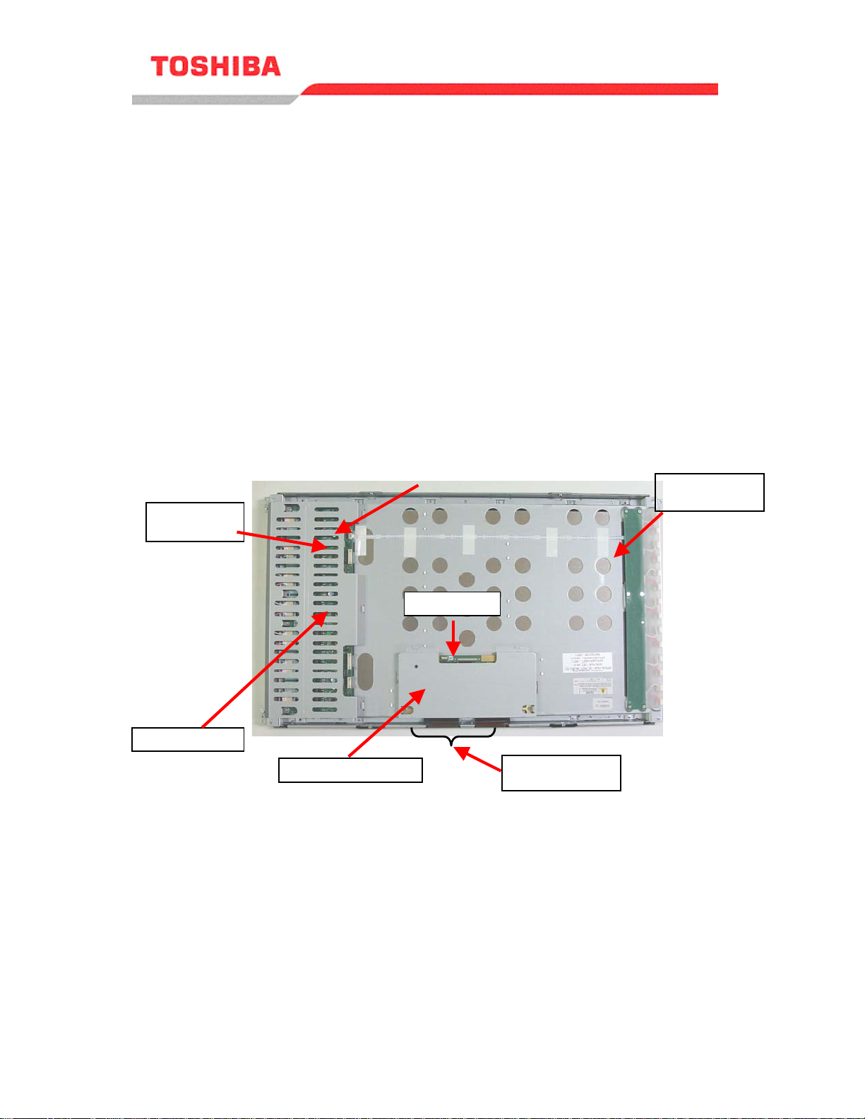
Model: 26HL84, 26WL46B/G/C/A/E/R/T
1. Cautions for Backlight Lamp Unit Replacement
The backlight lamps used in the listed Liquid Crystal Display (LCD) modules are
consumables. Follow the included replacement procedures when replacing these
components.
Disconnect AC power before starting the replacement procedure. The high
voltage applied to the backlight lamps produces an electrical shock hazard if
caution is not used when servicing this area.
Backlight lamp units are fragile and caution should be used when handling.
Ferrite cores are attached to the backlight lamp units with double-sided adhesive
tape. Use caution when removing these ferrite cores, as excessive force may
cause damage.
Where possible, replace backlight lamp units in a clean and dust-free environment.
TFT-LCD Module Bottom view
Return FFC
INV board
(HOT) side
INV board
(GND) side
INV cover
C board cover
C board
Flat cables
Ferrite cores
2004 LCD Television
Service Instruction
Page 1 of 1
2

2. Removing C Board Cover and C Board
2.1. Remove the two screws securing the C board cover.
2-2. Remove the two screws securing the C board. Remove the C board and
connectors, using caution to remove the ferrite cores.
Use caution when removing the ferrite
cores, as excessive force may cause
damage.
Service Instruction
2004 LCD Television
Page 2 of 12

3. Removing INV Cover and INV Board (HOT Side / GND Side)
3-1. Remove the return FFC connected to the INV board.
3-2. Remove the three screws securing the INV cover.
3-3. Disconnect the seven lamp unit connectors and remove the three screws
securing the INV board (HOT side).
3-4. Disconnect the seven lamp unit connectors and remove the seven screws
securing the INV board (GND side).
Service Instruction
2004 LCD Television
Page 3 of 12
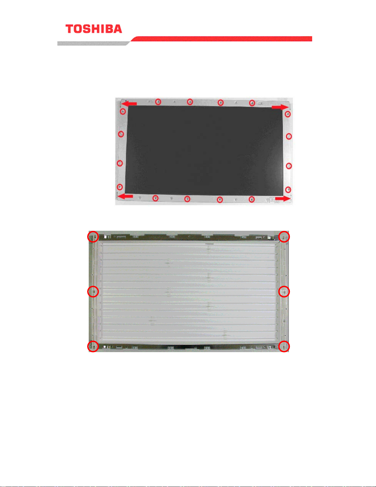
4. Removing Panel Unit and Lamp Holder
4-1. Remove the 20 screws securing the panel unit.
4-2. Remove the six screws securing the lamp holder.
Service Instruction
2004 LCD Television
Page 4 of 12

5. Replacing Lamp Units
5-1. Remove the old lamp units from the lamp clip, and replace them with new ones.
Be very careful not to break the lamp units when detaching/reattaching them. Keep
dust off the units.
Note: The seven lamp direct illumination system uses 14 CCFTs
(Cold Cathode Fluorescent Tubes) to provide backlighting for
the LCD display.
One lamp unit consists
of two lamps.
Small connector
Connected to INV board
(GND side)
Large connector
Connected to INV board
(HOT side)
Service Instruction
2004 LCD Television
Page 5 of 12
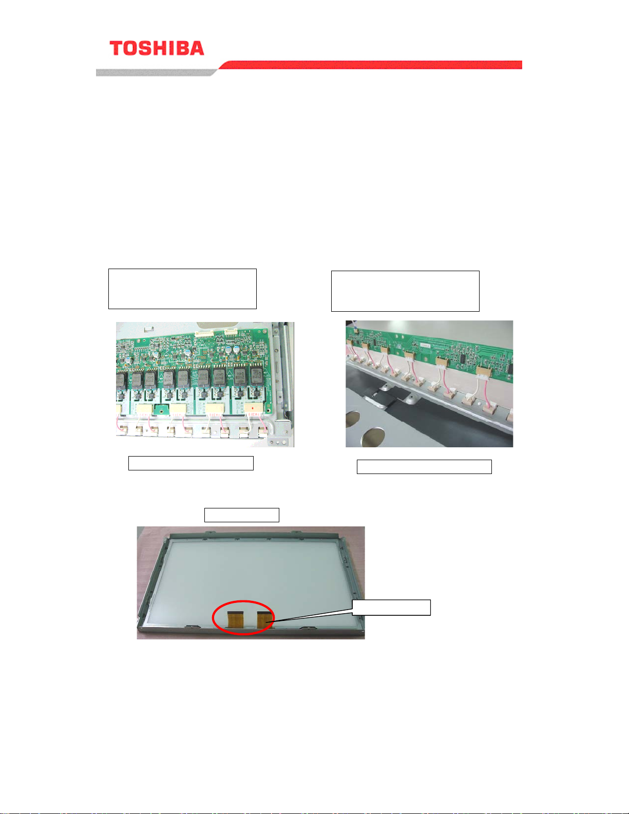
6. Assembly
6-1. Follow the lamp unit removal instructions in reverse order to re-assemble
the backlight lamp assembly. (Section2-5).
Assembly Cautions
Handle fragile lamp units with extreme caution.
Replace lamp units in a dust-free environment.
Do not bend or pinch flat cables when installing the panel unit.
Ferrite core may be damaged even by a slight shock. Attach ferrite cores
very carefully.
Connect the connectors securely to the INV board.
Connect small connectors
to the INV board (HOT
side).
Connect small connectors
to the INV board (GND
side).
INV board (HOT side)
INV board (GND side)
Panel unit
Flat cables
Service Instruction
2004 LCD Television
Page 6 of 12

Model: 32HL84, 32WL46B/G/C/A/E/R/T
1. Cautions for Backlight Lamp Unit Replacement
The backlight lamps used in the listed Liquid Crystal Display (LCD) modules are
consumables. Follow the included replacement procedures when replacing these
components.
Disconnect AC power before starting the replacement procedure. The high
voltage applied to the backlight lamps produces an electrical shock hazard if
caution is not used when servicing this area.
Backlight lamp units are fragile and caution should be used when handling.
Ferrite cores are attached to the backlight lamp units with double-sided adhesive
tape. Use caution when removing these ferrite cores, as excessive force may
cause damage.
Where possible, replace backlight lamp units in a clean and dust-free environment.
TFT-LCD Module Bottom view
Return FFC
INV board
(HOT) side
INV board
(GND) side
C board
C board cover
Flat cables
Ferrite cores
Service Instruction
2004 LCD Television
Page 7 of 12

2. Removing C Board Cover and C Board
2.1. Remove the two screws securing the C board cover.
2-2. Remove the two screws securing the C board. Remove the C board and
connectors, using caution to remove the ferrite cores.
Use caution when removing the ferrite
cores, as excessive force may cause
damage.
Service Instruction
2004 LCD Television
Page 8 of 12

3. Removing INV Cover and INV Board (HOT Side / GND Side)
3-1. Remove the return FFC connected to the INV board.
3-2. Remove the four screws securing the INV cover.
3-3. Disconnec t the eight lamp unit connectors from and remove the four s crews
securing the INV board (HOT side).
3-4. Disconnec t the eight lamp unit connectors from and remove the six screws
securing the INV board (GND side).
Service Instruction
2004 LCD Television
Page 9 of 12

4. Removing Panel Unit and Lamp Holder
4-1. Remove the 22 screws securing the panel unit.
4-2. Remove the six screws securing the lamp holder.
Service Instruction
2004 LCD Television
Page 10 of 12

5. Replacing Lamp Units
5-1. Remove the old lamp units from the lamp clip, and replace them with new ones.
Be very careful not to break the lamp units when detaching/reattaching them. Keep
dust off the units.
Note: The eight lamp direct illumination system uses 16 CCFTs
(Cold Cathode Fluorescent Tubes) to provide backlighting for
the LCD display.
Lamp unit consis t s
of two lamps
Small connector
Connected to INV board
(GND side)
Large connector
Connected to INV board (HOT side)
Service Instruction
2004 LCD Television
Page 1 1 of 12

6. Assembly
6-1. Follow the lamp unit removal instructions in reverse order to re-assemble
the backlight lamp assembly. (Section2-5).
Assembly Cautions
Handle fragile lamp units with extreme caution.
Replace lamp units in a dust-free environment.
Do not bend or pinch flat cables when installing the panel unit.
Ferrite core may be damaged even by a slight shock. Attach ferrite cores
Connect the connectors securely to the INV board.
Connect large connectors to
the INV board (HOT side).
very carefully.
Connect small connectors to
the INV board (GND side).
INV board (HOT side)
INV board (GND side)
Panel unit
Flat cables
Service Instruction
2004 LCD Television
Page 12 of 12

SIGNAL BOARD PD1753A1 (U901A)
TOP (COMPONENT) SIDE
1
9
PV22A
HD_HDMI
VD_HDMI
GND
CR
GND
CB
GND
Y
SCL1
SDA1
3.3V
5V-D
GND-D
9V-A
GND-A
5V-A
HDMI_RST
5V1
NC
KEY_1
KEY_GND
KEY_2
TUNER_GND
KEY_1
KEY_GND
NC
P520
GRV13
PR80
GRV14
2
GRV14
L_VARIOUT
R_VARIOUT
GND
GND
8
L_MONI
R_MONI
GND
GND_V_MONI
V_MONI
CV64
PV14
DVI_ Y
GND
3578
DVI_ PB
GND
DVI_ PR
64
GND
SDA1
SCL1
PV16
3.3V
1342
GND
NC
GND
5V-A
VDI_RST
68
75
13
52
PA0 5 A
231
PP17
PJ15A
GRV13
1
2
LV05
CV68
PK91
PA06A
CY526
CY506
RY513
CY506
RY513
RY532
RY533
RY534
RY532
EXT5-R
LV2 83
QV254
QV254
RY512
QY504
RY511
RY511
LV2 71
RY512
EXT5-CR
CV247
RV348
DV258
QY504
CV246
CV245
RV347
RV346
DV257
DV256
CY541CY538
+
EXT5-Y
EXT5-L
EXT5-CB
PV04
CC99
QV12
CV65
+
CV68
+
QV12
CV66
RV61
CV66
RV61
CV67
+
2
4
6
7
8
PV17
1
32
4
5
PV15
E
B
Q922
C928
CY539
RY590
CY590
CY591
LV1 3
LV2 73
CY540
RY590
CY590
CY591
DE99
CY508
XY502
RY585
RY585
RY591
RY591
RY592
RY592
CV253
RV330
DV24 4
RV331
DV24 9
CV254
DV25 0
CV255
RV332
DV244
RV330
CV253
DV249
CV254
RV331
GR96
GR96
RV332
19
DV250
20
DV25 1
DV25 2
CV256
DV251
DV252
CV256
+
32
33
CV255
RV337
RV337
RV338
RV338
CV257
LV253
LV252
LV251
+
+
CY524
QY501
CY524
CY525
XY501
CY526
CY525
30
CY502
CY502
RY533
RY534
16
QY501
1
CY508
15
RY521
RY520
RY521
RY520
CV247
RV348
DV25 8
1
51
+
CV246
RV347
DV25 7
CV245
RV346
DV25 6
LY1 0 5
CY116
QY102
RY103
CY109
52
CY116
RY103
QY101
EXT4-Y
LV2 82
CV250
CV249
CV251
CV251RV325
RV324
RV325
RV323
DV241
DV243
DV242
64
DV24 3
CV250
RV324
DV24 2
PV03
CV249
RV323
DV24 1
EXT4-L
EXT4-CB
+
CV258
LV270
CV243
+
CY110
RY105
CY111
CY112
CY105
RY102
CY106
RY104
RY101
LY1 0 2
LY1 0 2
CY107
LY1 0 0
LY1 0 0
LY1 1 2
CY109
9
RY105
CY110
CY111
CY112
CY105
LY1 0 5
RY102
CY106
RY101
RY104
QY102
LY1 0 4
16
CY115
QY101
LY1 0 1
LY1 0 1
CY115
LY1 0 4
+
RY110
QY103
CY108
CY108
LY1 1 2
CY103
CY101
8
QY100
1
CY103
+
QY100
CY102
LV2 72
CV82
CV80
+
C524
C524
1
24387101211956
9V
GND
GND
GND
CV79
+
PJ14A
GND
3.3VA
3.3VA
CV81
RV357
RV358
RV359
GJ128
GND
RV357
RV358
GND
GND
GND
GJ128
25
24
Y(1)
V_AV
C_AV
RV359
Pr(2),R
NC
GND
Y(2),G
VD
GNDNCGND
NC
Pb(2),B
NC
HD
NC
GND
Pr(1)
GND
GND
Pb(1)
+
13
GND
5V2
5V2
GND
3.3VA
GND
L289
+
39
40
CY104
CY118
CY114
CY113
EXT4-R
EXT4-CR
PV02
EXT1-V
EXT2-V
EXT1-L
EXT2-L
PV01
PD1753
EXT1-R
EXT2-R
P515B
-1
PV23B
1
2
R_HDMI-m
GND
DET_HP
L_HDMI-m
GND
R_DV1
L_DV1
SY_E3
E3_Y_GND
E3_C_GND
SC_E3
SW_E3
V_GND
V_E3
GND
L_E3
19
TUNER GND
R_E3
18
TUNER GND
23599267
RS44
RS42
RS38
RS39
CV08
RS40
1
16
RV10
CV09
RV29
LV0 9
RS40
8
9
RS48
P612A
CV09
RS48
RS47
3
RV09
RV09
RV10
CV23
QS05
RS44
1
QS05
RS35
RS47
RS45
RS37
CS25
2
1
GND
RV30
L_PC
R_PC
QV01
CV47
32
33
+
CV12
CV12
+
51
52
RS11
RS12
+
RS11
RS12
RS35
RV30
CV47
QS10
8
9
RS45
RS37
+
RV20
RV20
CV45
CV45
QV01
CV46
CC20
CV02
CC20
RV60
CV46
1
QS10
16
RS61
RS62
RS61
RS62
DV21
DV19
DV15
DV14
DV11
DV10
DV09
DV07 RV07
DV03 CV03
DV01
DV21
CC13
RV21
CV15
DV19
RV19
RV15
DV15
CV14
19
RV14
DV14
RV12
DV11
CV13
RV11
DV10
CV11
CV05
RV08
DV09
DV07
RV07
DV03
RV03
CV03
1
RV41
RV41
CC21
CC21
RV01
DV01
CV01
20
64
CC13
CV02
QV06
RV60
QV06
RV21
CV15
CV14
RV14
CV13
CV11
CV05
CV01
RV19
RV15
RV12
RV11
RV08
RV03
RV01
PS01
CV40
P120
LV4 2
2
1
43
QS06
RS41
RS42
RS41
8
QS06
CS21
CS21
9
CS22
CS22
RS39
RS49
RS50
RS38
RS50
C612
RS49
+
+
C653
C663
D613
D613
GJ113
RY109
CY117
RY107
LY1 0 3
RY106
QY103
CY101
RY110
CY104
CY118
CY114
CY113
GJ113
RY109
CY117
RY107
RY106
+
D612
R652
R652
LY1 0 3
D612
R655
R655
CV10
LV0 1
+
CV69
LV7 5
LV7 2
LV7 3
9V
PJ13A
PJ13A
9V
NC
13
5V2
5V212GND
GND
11
POWER_LCD
GND6GND
P OWER_TV
ACDETECT
5+4
7910 8
23
P810A
1
2
PP16
DET_FAULT
2
1
DET_HP
MUTE_AUDIO
POWER_SIG
1
MUTE_SPK
GND
GND
STOP_FAN
GND
3.3VA
3.3VA5GND
GND
12V
10 8 679
P104A
GND
GND
GND
GND
P811A
32V
5V2
9V
3.3VA
12V
SCL1
9V
9V
5V2
5V2
12V
SDA1
3.3VA
LV7 4
22
23
R_HDMI
213
GND
L_HDMI
P518B
PP15
LV0 3
LV04
LV0 2
RI_IN
GND
RI_OUT
798534 6
GND
21
LED
5V1
REM_IN
GND
REM_OUT
PB22A
5V1
GND
32V
324
1
P103B
GND
R_TV
GND
V_TV
GND
AFT1
L_TV
AFT2
TV_V_GND
GND
18
19
TV2V
AOUT
R_VARI
R_AV
NC
2
1
GND
L_AV
L_VARI
RESET_IMA
– 39 – – 40 –

SIGNAL BOARD PD1753A1 (U901A)
BOTTOM (FOIL) SIDE
19
18
19:TUNER_GND
18:TUNER_GND
17:R_E3
16:L_E3
P518B
14:V_E3
15:GND
11:SC_E3
10:E3_C_GND
12:SW_E3
13:V_E3_GND
RI_IN
GND
RI_OUT
GND
LED
5V1
REM_IN
GND
REM_OUT
18
19
TV2V
PV23B
8:E3_Y_GND
9:SY_E3
6:R_DV1
7:L_DV1
97
68
4
35
2
1
GND
GND
AOUT
AFT2
1
2
5:GND
4:DET_HP
QS21
RS86
RS85
GV12
V_TV
GND
TV_V_GND
2:L_HDMI-m
3:GND
RS87
RS84
RS88
QS19
RS86
RS85
GV13
GV12
PB22A
R_TV
L_TV
1:R_HDMI-m
RS83
RS83
RS84
QS21
QS19
GV13
GND
L_AV
AFT1
QS20
RS87
RS88
RS82
RS82
GRV88
GRV89
LV0 3
GRV84
GRV85
LV0 4
GRV86
GRV87
LV0 2
R_AV
NC
RESET_IMA
QS20
GND
CS37
CS37
RS81
CS36
GRV88
GRV89
GRV84
GRV85
GRV86
GRV87
5V1
R_VARI
L_VARI
P515B
RS81
CS36
PS01
1
R_HDMI
2
GND
3
L_HDMI
LV7 4
RV98
RV98
RV99
RV99
GND
GND
32V
24
31
22
2
1
23
P103B
P811A
SDA1
12V
5
SCL1
RS116
RS112
RS112
RS116
RS34
CV65
+
RV62
LV1 3
GRV29
GRV30
GRV31
DVI_ Y
GND
DVI_PB
GND
DVI_PR
GND
SDA1
SCL1
DE99
GND
GND
VDI_RST
LY5 0 2
CY513
CY535
RY541
RY548
RY545
RY545
CY537
RY547
CY537
RY547
RY561
R563
RY575
RY576
QY518
RY562
Y(2),G
GNDNCGND
Pb(1)NCGND
NC
Pr(1)
DB90
DB90
CS18
RS34
RS33
RS33
NC
RY543
RY577
RB90
RB90
R929
RY542
Pb(2),B
PR80
CS17
QS08
RS29
RV62
R929
QY514
QY520
GND
DB76
CS17
CS18
QS07
CV67
PV17
GR90
GR90
Q922
R563
Pr(2),R
RV66
DB76
RV66
2
4
6
8
PV15
1
3
5
E
B
C928
VD
QS18
QS07
RB76
QS17
RS29
1
3
5
7
2
4
6
GR91
PK91
GND
QS17
QS08
3.3V
5V-A
GR91
RB76
NCHDGND
RS80
NC
RS80
RS79
QS18
RS30
RS30
+
C927
+
RA80
PA0 6 A
RS79
GRV91
GRV91
CV64
C927
PA0 5 A
RA80
1
2
2
1
PV22A
9
8
LV0 5
GRV90
GRV90
PV14
HD_HDMI
2
VD_HDMI
GND
4
CR
53173
GND
6
CB
GND
824
Y
PV16
SCL1
SDA1
3.3V
5V-D
597
GND-D
9V-A
GND-A
5V-A
HDMI_RST
1
5V1
268
NC
KEY_1
4
KEY_2
TUNER_GND
P520
KEY_1
231
KEY_GND
NC
KEY_GND
CV38
LV3 7
RS57
RS57
QS12
CS28
RS15
GJ30
RV70
+
+
CV24
QB44
RV87
RV87
RV88RV100
RV88
LV7 2
GND
10 11
CV38
LV37
QS12
RS23
RS23
CS28
P612A
32
RS15
RV76
RB46
RB45
RB44
RB38
RB38
QB44
RV77
RV76
CV23
RV37
RS58
RS58
1:R_PC
CV08
LV0 9
RV77
CV24
CV10
CB47
QB46
CB42
CB42
RB40
5V2125V2
RV37
QS14
QS14
2:L_PC
RV29
RB41
RB47
RB39
13
CV39
LV38
LV3 8
RS60
RS60
3:GND
RB39
RB40
NC
CB46
CB43
PV02
EXT4-CR
EXT4-R
CV39
RV33
RV33
RV35
RV36
RV36
RV35
RS59
RS59
RS25
RS25
RS26
RS26
QS03
RS64
QS03
RS64
QS13
QS13
RS19
RS66
RS19
RS67
RS67
QS04
RS66
QS04
RS20
RS65
C612
+
C653
Q612
Q620
Q620
R631
R631
R630
R630
D614
D614
C662
C662
QV72
CB47
RB46
RB47
QV72
RB45
QB46
RB44
LV0 1
CV48
RJ40
RJ40
RJ41
RJ41
CV48
QB47
+
CV69
QB47
DV25
RB48
QB45
RB42
DV25
RV141
RV141
QV20
QV20
RB42
RB41
CB46
RB48
QB45
CB43
+
R662
R662
RS22
RS65
CS20
RS20
Q612
D611
CC06
R266
R266
RC05
CC06
RS56
RS55
QS09
RS56
QS09
RS55
CS20
CS15
CS15
CS16
CS16
RS21
CS14
CS14
RS21
RS22
CS13
CS13
R650
R650
R667
C661
C661
R661
D615
D611
D615
D617
D617
PV01
EXT1-R
EXT2-R
RC04
RC04
CC04
CC04
RV17
RV17
CS07
RS07
RS08
CS08
CS06
RS06
RS05
CS05
RV06
RV06
CV04
DV05
RS04
CS04
CS03
RS03
QV14
CV78
RV97
RV96
3.3VA863.3VA
GND
GND
9
7
3.3VA
32V
12V
3.3VA
9V9V9V
5V2
12V
EXT2-L
EXT1-L
RC02
RC03
RC03
RC02
CC03
CC02
CC02
CC03
CS27
CS27
CS26
CS26
RS74
RS75
RS74
RS75
RS63
RS63
CS51
RS76
RS76
RS52
CS10
CS09
CS10
CS09
CS11
CS11
RS09
DV02
RS10
RS09
CV06
DV02
CV06
RS07
CS07
RS08
CS08
RS06
CS06
CS05
RS05
CV04
DV05
CS04
RS04
CS03
RS03
CS23
CC77
CC78
RS01
RS02
CC77
RS02 CS02
CC78
RS01
CS02
CS01
RV95
RV94
RV94
RV95
CV73
QV13
CV73
CV78
QV14
RV92
RV93
STOP_FAN
10
5V2
5V2
QV13
RV97
RV96
RV93
RV92
P120
2
4
3
1
RV101
RV100
LV7 5
POWER_SIG
P OWER_TV
ACDETECT
2
1
3
GND
GND
GND
MUTE_SPK
DET_FAULT
GND
DET_HP
GND
GND
MUTE_AUDIO
RC01
RC01
CC01
CC01
RS18
RS18
RS17
RS17
+
CS51
RS52
CS12
RS36
RS36
CS12
RS10
CS23
CS01
RV91
RV91
RV79
CV42
+
RV101
POWER_LCD
4
2
1
RS46
RS46
QS15
QS15
RS13
CS24
RS51
GND
P104A
QV73
RV40
RS14
RS13
CS24
RS51
GND
65
P810A
RV79
CV42
RV89
RV90
RV90
LV7 3
RS14
CV07
QV73
CV40
LV4 2
EXT2-V
RV40
RS24
RS24
CS25
RS54
RS54
RV73
RS53
RS53
CS31
RV28
QV09
RV89
9V
EXT1-V
RV34
CS29
QV70
CV07
CS31
RV28
+
RV78
RV78
CB40
RV73
CB40
9V
87
QV70
QV09
QS11
RV70
CS29
RS16
RV26
RV34
QS11
1
RS16
GJ30
CS30
CS30
RV27
RV27
RV26
CB45
CB45
RB43
RB43
RB37
RB37
CB41
CB41
GND
9
RC05
+
C663
R667
R661
RC06
RC06
CC05
CC05
EXT4-CB
+
L289
GR289
GR289
R265
CY102
PV03
R265
CY107
LV2 82
EXT4-L
LV2 70
RV72
QV71
+
EXT4-Y
R264
R264
RV370
RV368
RV369
RV371
RV368
RV370
RV369
RV371
+
CV258
CV239
CV243
CV239
+
RV72
QV04
RV86
QV04
RV75
QV71
RV74
RV85
RV71
RV256
RV256
A
RY550
QY515
CY536
RY551
RY514
CY501
RY501
CY504
RY539
RY540
JY508
JY509
QY508
QY509
+
CV82
C522
C522
13
12 4
5V2
GND
LV2 83
DS-7405
23547608
CV248
CV248
CV244
CV244
CV238
CV238
QV247
RV255
RV255
QV247
RV353
RV252
RV254
RV252
RV254
RV86
RV75
RV74
RV253
RV85
LV2 71
QV246
RV71
QV246
RV253
GRV21
+
CY541
RY527
RY528
RY552
LY0 1 3
LY0 1 3
CY514
CY512
CY518
RY538
JY507
QY507
RY537
RY531
RY555
CV80
+
C523
C523
911 7
8
10
3.3VA
GND
5V2
GND
CV263
CV263
RV353
GRV21
LY0 1 2
GRV23
LY0 1 2
QY509
RY555
R288
RV375
CV261
CV261
RY540
RY531
+
3.3VA
RV375
RV352
GRV23
+
RY537
PJ14A
EXT5-CR
R288
RV374
RV374
CV252
CV259
RV352
RV351
GRV22
GRV22
RY527
RY528
QY513
CY538
RY508
RY508
RY539
JY509
JY508
QY508
RY530
RY530
RY554
CV79
6
3.3VA
CC08
CC08
RV373
RV373
CV252
CV259
RV259
RV351
GRV39
GRV39
QY513
RY509
RY510
RY536
5
GND
EXT5-R
RC08
RC07
RC07
RV372
RV372
RV258
RV259
RV258
RV260
RV260
QV249
CV237
CV237
RY525
RY526
QY512
RY518
RY518
QY510
QY503
RY509
QY503
RY510
RY538
JY507
QY507
RY535
RY529
RY553RY554
RY553
+
31
GND
GND
RC08
RV257
QV248
QV249
RY525
RY526
RY515
RY515
RY536
RY535
RY529
CC07
QV248
QY512
2
9V
CC07
L_VARIOUT
R_VARIOUT
GND
GND
L_MONI
R_MONI
GND
GND_V_MONI
V_MONI
RV257
QY510
CY501
CY505
XY501
CV81
GND
EXT5-CB
R287
R287
RV356
RV356
RV355
RV354
RV354
RV261
RV261
RY517
RY517
A
RY550
RY519
RY519
RY514
RY501
CY504
RY502
CY505
RY573
PV04
+
RV355
RY523
RY524
RY523
RY524
CY582
RY505
RY573
EXT5-L
CV257
QY511
QY511
CY536
RY551
CY512
RY503
RY503
RY507
RY507
QY515
RY502
QY502
CS39
RS103
RS103
RY516
CY518
RY504
CY582
RY505
QY502
PJ15A
LV2 53
GRV58
GRV58
GRV59
GRV56
GRV56
GRV57
LV2 52
GRV54
GRV55
GRV55
LV2 51
RY516
RY552
CY514
25
RS27
RS27
RS28
RS28
CS39
R286
GRV28
GRV30
CY516
CY516
CY517
CY517
RY576
QY518
GRV25
GRV25
24
RY581
RY560
RY575
EXT5-Y
R286
RS104
RS104
+
+
CY513
CY535
RY541
RY581
RY560
RY562
LV2 72
GRV24
GRV24
GND
QS16
LY5 0 1
CY515
CY515
RY577
V_AV
QS16
GRV59
GRV57
GRV54
LY501
RY542
RY548
XY502
QY520
GRV27
GRV27
GND
C_AV
CC99
CS34
CS34
CS35
CS35
CY540
LY502
CY539
RY543
QY516
RY504
GRV26
GRV26
GND
Y(1)
LV2 73
GRV29
GRV28
GRV31
QY514
QY516
RY561
GND
– 41 – – 42 –

FRONT/AV BOARD PD1753A2 (U901B)
TOP (COMPONENT) SIDE
FRONT/AV BOARD PD1753A2 (U901B)
BOTTOM (FOIL) SIDE
AV2 BOARD PD1753A3 (U901C)
TOP (COMPONENT) SIDE
AV2 BOARD PD1753A3 (U901C)
BOTTOM (FOIL) SIDE
PD1753
PS02
DVI-L
DVI-R
23599267
R_HDMI-m
GND
PV23A
1
2
L_HDMI-m
L_HP
R_HP
HP_GND
GND
DET_HP
1
2
3
L_DVI
R_DVI
P613B
Y_E3
GND
GND
S-SW_E3
-2
C_E3
GND
V_E3
CY650
GND(Audio)
L_E3
DV12 0
PV61
R_E3
TUNER
GND
19
18
TUNER GND
PV60
P661
E3-R
E3-L E3-V
PV60
RV121
RV120
RV120
E3-L
RV122
RV122
RV121
E3-V
GR604
E3-R
GR604
P661
GR605
RC16
RC15
CV121
PV61
CV121
GRV16
19
18
RC16
RV129
RV129
GRV16
RC15
CC09
GR605
CC10
CC09
CC10
R690
R690
R688
R688
CY650
D652
D653
D653
19:TUNER GND
16:L_E3
17:R_E3
18:TUNER GND
DV12 0
D652
C606
C606
C605
C605
DS-7405
23547608
7:L_DVI
8:GND
9:Y_E3
10:GND
11:C_E3
12:S-SW-E3
13:GND
14:V_E3
15:AudioGND
1
2
PV23A
GSR11
GSR11
GSR10
GSR10
P613B
1
L_HP
2
R_HP
3
HP_GND
6:R_DVI
GSR06
4:DET_HP
5:GND
RC12
RC12
GSR06
1:R_HDMI-m
2:L_HDMI-m
3:GND
CC14
CC14
RC11
RC11
GSR05
DVI- L
CC15
DVI- R
GSR05
CC15
PS02
23599267
PD1753
PV22B
82
9
PV05
1
-3
DS-7405
23547608
PV05
2
CC19
CC19
LC03
LC03
RS31
CC12
LC02
LC02
CC18
LC04
LC04
CC11
RS32
LC01
PV22B
RS31
CC18
CC11
RS32
LC01
CC12
8
91
POWER SW BOARD PD1753A4 (U901D)
TOP (COMPONENT) SIDE
PD1753
321
-4
23597608
S801
PA0 6 B
POWER SW BOARD PD1753A4 (U901D)
BOTTOM (FOIL) SIDE
DS-7405
23547608
S801
32
1
PA06B
– 43 – – 44 –

IR/LED BOARD PD1753A6 (U901F)
TOP (COMPONENT) SIDE
IR/LED BOARD PD1753A6 (U901F)
BOTTOM (FOIL) SIDE
CB60
BB01
QB51
CB61
8
CB59
5
+
CB55
CB53
1
CB51
4
++
CB52
KB01
+
CB01
DB51A
DB51
D-REWRITE BOARD PD1753A7 (U901G)
23599267
PD1753 -6
CB56
+
OUT
GND
IN
GND
5V14LED
5
6
9
7
PB22B
TOP (COMPONENT) SIDE
DB01A
DB01
REM IN
3
GND
REM OUT
12
LB52
PJ91A
PJ93A
CB58
+
CB57
DB03A
DB03
RB65
DB53
RB64
RB65
DB53
CB57
RB64
RB74
RB74
QB55
CB58
QB55
RB66
+
RB66
LB52
DB03A
DB03
QB01
QB01
RB05
PB22B
GND
REM
OUT
IN
RB01
RB01
RB05
RB71
DB01
RB71
DB01A
RB70
RB70
RB04
QB54
RB04
QB54
+
LB51
LB51
CB56
712345
GND
REM
5V1
GND
OUT
LED
CB61
RB62
RB69
RB67
RB69
RB67
RB62
QB52
QB52
QB53
QB53
RB73
RB73
CB59
DB54
RB72
DB54
RB72
CB55
IN
DS-7405 23547608
BB02
RB56
CB53
8
RB58
RB59
+
5
RB60
RB58
RB59
RB60
QB51
CB54
RB56
CB54
RB51
RB57
RB57
RB51
1
CB51
RB55
4
RB55
CB52
+
DB51
RB54
RB53
+
DB51A
RB52
RB52
RB54
RB15
RB15
KB01
DB52
DB52
RB63
RB63
RB53
CB60
CB01
RB19
+
RB19
D-REWRITE BOARD PD1753A7 (U901G)
BOTTOM (FOIL) SIDE
PJ91B
5
5
4
4
3
3
2
2
1
1
PJ93B
5
5
4
4
3
3
2
2
1
1
PJ91B
5
4
3
2
1
PJ93B
5
4
3
2
1
PJ91A
4
2
PJ93A
5
3
1
5
3
1
4
2
POS UP
SA01
PJ94A
PJ94B
11
PJ94A
1
PD1753 -7
23599267
KEY BOARD PD1753A5 (U901E)
TOP (COMPONENT) SIDE
PD1753
POS DOWN
SA02
SA03
-5
VOL UP
GND
6:MAIN
5:KEY-2
GND
4:MICON
3:KEY-1
23599267
VOL DOWN
SA04
61
2:NC
1:NC
MENU
SA06
PA0 5 B
VIDEO
SA07
1
3
5
7
9
11
PJ94B
1
3
5
7
9
11
DS-7405
23547608
KEY BOARD PD1753A5 (U901E)
BOTTOM (FOIL) SIDE
DS-7405
POWER
SA05
POWER
SA05
VIDEO
SA07
MENU
SA06
RA75
RA76
RA75
RA76
5:KEY-2
1:NC
6:MAIN
4:MICON
3:KEY-1
2:NC
GND
GND
4
21
VOL DOWN
SA04
PA05B
6
23547608
RA71
VOL UP
SA03
RA73
RA73
POS UP
SA01
POS DOWN
SA02
RA72RA71
RA72
– 45 – – 46 –

TN/A-OUT BOARD PD1754A1 (U902)
TOP (COMPONENT) SIDE
TN/A-OUT BOARD PD1754A1 (U902)
BOTTOM (FOIL) SIDE
P517
PIP OUT
ADR SEL
H002
H001
GR113
GR113
R-OUT
L-OUT
W-OUT
L-IN
PIP IN
R=IN
TV-L
AFT-1
TV-R
RESET
V-OU T
RF AGC
IF IN
GR110
GR110
SDA
SW2
GND
SCL
GND
SW1
GND
SDA
AGC
9V
5V
5V
9V
NC
IF1
BTL
SCL
GRS01
CS504
GR132
12
18
D132
C133
111
R135
GR132
L102
PK05
PK06
D132
R133
P105
RS500
GRS01
RS506
DS102
RS515
GR622
GR621
+
L132
L132
R131
R131
L133
L133
R132
R132
C133
+
+
GR04
R133
Q131
Q131
R134
R135
R134
C105
GR01
GR01
+
L105
GR03
GR03
Q152
R151
R151
3
1
2
9V
RF-SW
GND
P516
R614
D629
D646
D642
C625
3
C691
C691
R-_AMP
RD237
Q677
R615
R677
Q672
R673
D646
D642
C627
C623
C625
C648
4
R+_AMP
R601
Q677
C635
P601
+
C665
R680
R672
Q672
R673
C678
C678
R645
R645
R604
R604
+
C627
C623
R623
R623
C646
C646
BD01
DD202
DD201
RD235
CD233
CS501
+
45
GR112
GR112
GR623
GR623
+
CS503
QS102
QS102
C127
1
CS502
CS502
8
+
RFAGC
VT(NC)
ADS
SCL
SDA
NC
R600
27262524232221201918171615141312
C131
+5V
NC
+32V
+
NC
IF
L134
+
IF AGC
C132
L131
111098765423
C105
+
1
C108
NC
NC
V
NC
C104
+
+
L101
A
TU
GR111
GR111
C172
+
P105
C102
9V
A OUT
GND
AFT
RFAGC
V OUT
PT01
L102
PT01
31
+
RT01
RT01
L105
9V
RF-SW
GND
1
2
3
TP-12TP-12A
PK05
PP22
HY01
Q630
54
8
1
+
+
C640
312
P613A
GND
R_HP
CD228
+
CD225
+
LD204
QD206
L135
RD228
CD201
LD201
+
LD201
CD213
CD203
CD202
QD206
RD228
QD202
CD201
RD205
RD210
28
1
RD210
CD203
CD202
5
CD222
CD222
1
QD203
QD203
RD204
RD205
QD202
CD205
CD204
CD204
CD205
RD117
RD117
RD112
RD112
5
CD113
QD201
LD204
CD220
CD221
CD220
RD204
RD201
+
QD102
CD117
4
QD102
CD113
+
L_HP
17
RD220
CD221
CD117
RD220
25
RD221
15
14
L643
C688
+
C615
C641
C642
RD221
RD222
RD223
XD01
16
QD201
24
RD222
RD224
RD223
RD201
RD203
RD239
CD207
RD203
RD239
CD206
CD206
CD210
1
RD120
RD120
CD114
RD115
8
RD115
RD224
14
CD207
QD204
+
CD114
RD229
9
8
32
RD229
RD206
CD223
1
CD209
DD101
DD101
RD130
RD102
RD130
CD215
RD216
RD215
RD202
RD225
RD206
CD223
QD204
RD225
1
RD226
CD120
CD120
RD102
RD107
GRD02
GRD01
RD226
CD214
RD211
8
7
RD248
RD248
CD234
QD101
4
QD101
5
CD106
CD106
RD107
D627
D628
RD211
28
CD103
CD103
GRD02
GRD01
C636
L620
L622
+
15
CD235
CD234
PD1754
P516P515
PK06
23599268
+
C614
QD208
8
R613
+
RD212
CD235
CD215
RD216
RD215
RD202
RD212
QD208
1
RD110
CD107
RD105
18
L622
D628
L620
QD207
RD105
CD107
C666
C614
19
C613
C613
R612
R613
D626
D625
QD207
RD110
R612
R610
D626
+
R609
R610
D625
GR608
GR608
GND
GND
GND
GND
12V
12V
12V
12V
R614
R615
R672
R680
R677
D629
L640
+
C665
C687
C610
C610
R609
L655
C608
C603
C603
D657
C608
L655
C601
Q610
36
+
PP21
L640
GND
D657
C630
C630
GND
GND
C601
GND
1
12V
12V
Q610
12V
+
8
7
6
5
4
3
2
1
12V
P809A
P809A
8
7
6
5
4
3
2
1
C629
C629
C635
D623
D622
D622
D623D627
D624
D621
D621
D624
L623
L623
L625
L625
GR607
GR607
1
432
P601
L-_AMP
R-_AMP
L+_AMP
R+_AMP
14
BD01
1
2
P104B
3.3VA
R_AV
R_TV
V_TV
GND
GND
12V
SCL1
GND
GND
GND
M-AUDIO
DET_HP
GND
GND
GND
5V2
5V2
5V2
32V
9V
9V
9V
3.3VA
12V
SDA1
23
22
2
1
L_VARI
GND
NC
RST-IMA
L_AV
AFT1
L_TV
V_GND
AFT2
AOUT
TV2V
19
18
P103A
1
DET_FAULT
MUTE_SPK
XD02
GND
R601
R_VARI
TV-GND
C602
MUTE_AUDIO
DET_FAULT
DET_HP
MUTE_SPK
GND
GNDGND
GND
GND
GND
GND
5V2
5V2
5V2
32V
9V
9V
9V
3.3VA
3.3VA
12V
12V
SCL1
SDA1
P103A
C602
C648
C693
C693
1
2
C692
C694
C694
C692
L+_AMP
L-_AMP
CD231
1
2
P104B
22
23
2
1
L_VARI
R_VARI
GND
NC
RESET_IMA
R_AV
L_AV
GND
AFT1
R_TV
L_TV
TV-GND
TV-V_GND
V_TV
AFT2
GND
AOUT
GND
TV2V
18
19
C687
Q680
Q680
C604
DD206
CD230
RD104
RD103
C624
C624
C622
LD203
R676
Q671
R646
R646
C604
C621
C621
RD238
DD201
XD02
CD124
CD123
CD101
R670
R676
C611
D656
C622
R671
C677
C677
C611
R611
CD231
R681
R670
Q671
D656
DD202
DD206
LD203
CD230
CD233
CD123
CD118
CD101
R681
R611
C649
+
RD235
CD124
LD103
+
C666
L645
L643
C688
L645
+
R671
C615
Q679
Q678
Q678
Q679
R619
R619
R618
D620
R618
D620
R616
R616
R642
D643
R642
D643
+
C636
C620
C620
R620
R620
C647
C647
C649
CD232
DD204
DD203
RD234
CD214
CD218
RD238
CD232
DD204
RD214
DD203
RD237
RD213
RD234
RD214
RD236
RD213
RD251
RD243
LD205
DD205
RD240
LD205
RD236
RD251
DD205
RD240
LD103
CD119
LD101
LD101
CD118
CD119
RD104
RD103
CD102
CD105
RD101
RD108
RD109
CD104
RD106
CD104
CD105
CD102
RD109
RD108
RD101
DS-7405
23547609
RD217
RD243
RD116
RD106
RD218
RD217
CD218
RD219
CD209
RD118
RD119
D640
D672
R663
+
CD116
R660
C667
C668
XD01
RD218
RD219
C644
RD250
RD250
RD208
RD207
CD210
+
RD119
R664
+
C641
+
C642
P613A
R641
CD216
CD217
CD217
CD219
CD219
RD209
CD115
CD115
CD116
RD118
RD114
C631
R695
R664
RD116
RD114
RD113
Q676
C669
R678
C667
C668
C644
1
L_HP
CD216
LD202
LD202
RD111
RD113
RD111
R686
D673
D641
D641
2
R640
R641
R_HP
CD227
CD226
CD208
RD230
CD208
DD210
QD205
CD211
CD211
CD111
CD112
C631
D673
D672
R663
CD227
RD232
RD207
CD122
CD111
CD112
R686
Q676
C669
3
GND
+
CD226
RD230
DD210
QD205
CD122
R687
R687
R678
R695
R660
R674
R674
4
D640
+
CD228
RD227
RD233
RD233
RD232
RD208
RD209
DD209
LD102
1
C645
R640
CD224
RD227
CD212
LD102
D608
C640
CD224
+
CD212
Q675
C679
C632
5
8
RD249
R679
R696
C645
RD249
DD209
+
CD121
CD121
Q675
C679
R679
C632
C672
C673
C643
C643
CD225
CD213
D608
R696
C672
Q630
C673
VT(NC)
IF AGC
AFT
GR131
RFAGC
ADS
SCL
SDA
NC
+5V
NC
+32V
NC
IF
A OUT
RFAGC
V OUT
GR131
HY01
9V
GND
L135
TP-12
TP-12A
RS501
RS506
Q152
Q151
RS500
RS507
L134
C132
C108
Q151
RS505
C131
L131
C104
C102
L101
C172
C127
GR04
+
GR02
CS504
GRS02
R600
GR02
R150
R152
CS505
R150
CS501
CS510
RS501
DS102
RS515
RS504
GRS02
R104
C161
+
+
+
R152
P515
CS510
C124
C122
C162
+
RS516 RS517
RS516 RS517
CS505
RS504
GR621
GR622
RS507
RS505
+
CS503
C126
27
C126
25 24 23 22 19 13 12
C124
C122
21 20 18
C162
R104
C161
11 9 8 3 1
10
25467
C103
C103
D102
C101
D102
C101
SDA
SCL
A
R110
R110
11
1
26
GR106
GR105
9V
R-OUT
GND
L-OUT
PIP OUT
W-OUT
R121
R120
GND
GR106
GR105
AFT1
TV-R
5V
SW2
RESET
5V
V-OU T
SW1
RF AGC
9V
NC
IF IN
GND
IF1
NC
BTL
NC
V
NC
TU
AGC
R121
R120
L-IN
PIP IN
ADR SEL
TV-L
R102
L104
R103
L103
R-IN
R102
L104
R103
L103
SDA
SCL
H002
H001
P517
– 47 – – 48 –

SCALER BOARD PD1755B1 (U903)
TOP (COMPONENT) SIDE
– 49 – – 50 –

SCALER BOARD PD1755B1 (U903)
BOTTOM (FOIL) SIDE
– 51 – – 52 –

CIRCUIT BLOCK DIAGRAM
E1
E2
E3
CS_E4
CS_E5
DVI
AV
QV01
CXA2069Q
CS
QV254
MM1519XQ
V_AV_MC SYNC_M
V_AV
C_AV
V_PIP
SYNC_S
C_AV_SUB
Y1
SUB-Y
COMB
QY100
TC90A45F
Y_COMB_S
C_COMB_S
SUB CD
QY501
TA1340F
HD
VD
G-HYPER
DVCD
QZ501
TC90A92
A/D
QU100
A/D
QX100
I/P
QX300
GM6010
A PORT B PORT
NORMAL CS CVBS
D/W SUB MAIN
YPbPr1
CVBS/Y
C
YPbPr2
CTRL
YPbPr1
CVBS/Y
PJ15A
YPbPr2
PJ13A
C
MST9883M
TC90A92AFG
42MHz
3ch A/D
MST9883M
CTRL
3ch A/D
YCbCr
16
I2C
TV MICRO
MN102HF75KBF
EEPROM
Y/C
8
24
I2C
64Kbit
2M x 32Mbit
SDRAM
256Kbit
EEPROM
RGB
4:2:2
G-Hyper MICRO
TMPA8700CSF
ADC08060
ADC08060
ADC08060
RGB
5:6:5
1M x 32bit
DDR-SDRAM
133MHz
TC90A94TBgm6015
I2C
BEP MICRO
M30626FHPGP
128Kbit
EEPROM
RGB 8:8:8
50/60Hz,OS_ON/OFF
THC63LV
DM83R
MK1707STR
133MHz
ICS487G-35T
13.5MHz
TEMP
BL_ON/OFF,DIM
PJ100
LVDS
PJ12 PJ101
PJ102
– 53 – – 54 –
SCHEMATIC DIAGRAM
MODEL : 26HL84
WARNING: BEFORE SERVICING THIS CHASSIS, READ THE "X-RAY RADIATION PRECAUTION", "SAFETY
PRECAUTION" AND "PRODUCT SAFETY NOTICE" ON THE MANUAL FOR THIS MODEL.
CAUTION: The international hazard symbols " " in the schematic diagram and the parts list designate components
which have special characteristics important for safety and should be replaced only with types identical to those in the
original circuit or specified in the parts list. The mounting position of replacements is to be identical with originals.
Before replacing any of these components, read carefully the PRODUCT SAFETY NOTICE on the MANUAL for this
model. Do not degrade the safety of the receiver through improper servicing.
NOTE:
1. RESISTOR Resistance is shown in ohm [K = 1.000, M = 1.000.000]. All resistors are 1/6W and 5% tolerance
2. CAPACITOR Unless otherwise noted in schematic, all capacitor values less than 1 are expressed in
carbon resistor, unless otherwise noted as the following marks.
1/2R = Metal or Metal oxide of 1/2 watt 1/2S = Carbon compsistion of 1/2 watt
1RF = Fuse resistor of 1 watt 10W = Cement of 10 watt
±10% G = ±2% F = ±1%
K =
µ
the values more than 1 in pF.
All capacitors are ceramic 50V, unless otherwise noted as the following marks.
Electolytic capacitor Mylar capacitor
F, and
3. The parts indicated with "
4. Voltages read with DIGITAL MULTI-METER from point indicated to chassing ground, using a color bar signal with
all controls at normal, line voltage at 220 volts.
5. Waveforms are taken receiving color bar signal with enough sensitivity.
6. Voltage reading shown are nominal values and may vary
" have special characteristics, and should be replaced with identical parts only.
±20% except H.V.
– 55 –

SCHEMATIC DIAGRAM STRUCTURE:
– SIGNAL Circuit CONNECTOR [ SHEET– 1/7 ] .................. 1/57
– AV [ SHEET– 2/7 ] .................. 2/57
– TERMINAL [ SHEET– 3/7 ] .................. 3/57
– COLOR DIFFERENCE SWITCHING [ SHEET– 4/7 ] .................. 4/57
– V/C [ SHEET– 5/7 ] .................. 5/57
– HDMI_VARI [ SHEET– 6/7 ] .................. 6/57
– Audio-MUTE [ SHEET– 7/7 ] .................. 7/57
– TN-AOUT Circuit CONNECTOR [ SHEET– 1/8 ] .................. 8/57
– TIF & MA [ SHEET– 2/8 ] .................. 9/57
– IMA MOPULE [ SHEET– 3/8 ] ................ 10/57
– A-OUT [ SHEET– 4/8 ] ................ 11/57
– HP-AMP [ SHEET– 5/8 ] ................ 12/57
– TEMP SENSOR [ SHEET– 6/8 ] ................ 13/57
– LipSync DIGITAL PART [ SHEET– 7/8 ] ................ 14/57
– LipSync ANALOG PART [ SHEET– 8/8 ] ................ 15/57
– CONT Circuit KEY [ SHEET– 1/2 ] ....................................................... 16/57
– POWER SW [ SHEET– 2/2 ] ....................................................... 17/57
– DATA_REWRITE Circuit ............................................................................................................... 18/57
– FRONT-AV Circuit AV-1 [ SHEET– 1/2 ] ................................................................... 19/57
– AV-2 [ SHEET– 2/2 ] ................................................................... 20/57
– IR-PASS/RMT/LED Circuit ............................................................................................................ 21/57
– SCALER Circuit DIGITAL INPUT [ SHEET– 1/36 ] .............. 22/57
– CAPTURE INPUT [ SHEET– 2/36 ] .............. 23/57
– MEMORY CONNECTION [ SHEET– 3/36 ] .............. 24/57
– PLL [ SHEET– 4/36 ] .............. 25/57
– OSD [ SHEET– 5/36 ] .............. 26/57
– IIC [ SHEET– 6/36 ] .............. 27/57
– US OSD SYNC GENERATOR [ SHEET– 7/36 ] .............. 28/57
– POWER [ SHEET– 8/36 ] .............. 29/57
– SUB MICOM (1) [ SHEET– 9/36 ] .............. 30/57
– SUB MICOM (2) [ SHEET– 10/36 ] ............ 31/57
– SUB MICOM (3) [ SHEET– 11/36 ] ............ 32/57
– LVDS OUT [ SHEET– 12/36 ] ............ 33/57
– POWER CONNECTOR AND DIMMING [ SHEET– 13/36 ] ............ 34/57
CONNECTOR BETWEEN SIGNAL BOARD
–
– EMI FIL 2 [ SHEET– 15/36 ] ............ 36/57
– LVDS POWER AND OTHERS [ SHEET– 16/36 ] ............ 37/57
– LVDS OUT (SHARP LCD) [ SHEET– 17/36 ] ............ 38/57
– CONNECTOR [ SHEET– 18/36 ] ............ 39/57
– 3CHADC1_LPF [ SHEET– 19/36 ] ............ 40/57
– 3CHADC2_LPF [ SHEET– 20/36 ] ............ 41/57
– DVCD_LPF [ SHEET– 21/36 ] ............ 42/57
– 3CHADC HD/VD [ SHEET– 22/36 ] ............ 43/57
– 3CHADC1 [ SHEET– 23/36 ] ............ 44/57
– 3CHADC2 [ SHEET– 24/36 ] ............ 45/57
– DVCD TC90A92AFG [ SHEET– 25/36 ] ............ 46/57
– DVCD_POWER [ SHEET– 26/36 ] ............ 47/57
– GENESIS-1 [ SHEET– 27/36 ] ............ 48/57
– GENESIS-2 [ SHEET– 28/36 ] ............ 49/57
– SDRAM [ SHEET– 29/36 ] ............ 50/57
– GENESIS_POWER [ SHEET– 30/36 ] ............ 51/57
– GENESIS_CPU [ SHEET– 31/36 ] ............ 52/57
– OSD MICON 1/4 [ SHEET– 32/36 ] ............ 53/57
– OSD MICON 2/4 [ SHEET– 33/36 ] ............ 54/57
– OSD MICON 3/4 [ SHEET– 34/36 ] ............ 55/57
– OSD MICON 4/4 [ SHEET– 35/36 ] ............ 56/57
– DC/DC CONVERTER [ SHEET– 36/36 ] ............ 57/57
[ SHEET– 14/36 ] ............ 35/57
– 56 –

SPECIFICATIONS
MODEL 26HL84
Television System NTSC standard
Channel Coverage VHF: 2 through 13
UHF: 14 through 69
Cable TV: Mid band (A-8 through A-1, A through I)
Super band (J through W)
Hyper band (AA through ZZ, AAA, BBB)
Ultra band (65 through 94, 100 through 125)
Power Source 120 V AC, 60 Hz
Power Consumption 115W (average)
Number of picture Elements 1366 (H) dots x 768 (V) dots
Audio Power 10 W + 10 W
Speaker Type Two 2-3/8 x 4-3/4 inches (60 x 120 mm)
Video/Audio Terminals S-VIDEO INPUT
Y: 1 V (p-p), 75 ohms, negative sync.
C: 0.286 V (p-p) (burst signal), 75 ohms
VIDEO/AUDIO INPUT
VIDEO: 1 V (p-p), 75 ohms, negative sync.
AUDIO: 150 mV (rms) (30% modulation equivalent, 22k ohms or more)
ColorStream® (component video) INPUT
Y: 1V (p-p), 75 ohms
PR: 0.7 V (p-p), 75 ohms
PB: 0.7 V (p-p), 75 ohms
AUDIO: 150 mV (rms), 22k ohms or more
VIDEO/AUDIO OUTPUT
VIDEO: 1 V (p-p), 75 ohms, negative sync.
AUDIO: 150 mV (rms) (30% modulation equivalent, 2.2k ohms or less)
VARIABLE AUDIO OUTPUT
0300 mV (rms) (30% modulation equivalent, 2.2k ohms or less)
DVI/HDCP INPUT
HDCP complian
E-EDID* 1.3 compliant
DVI-D uncompressed, high-speed, digital single-link connection
Suggested input scan rates: 1080i, 720p, 480p, 480i
Headphones jack 3.5 mm stereo
TheaterLink OUTPUT: 3 V (p-p), 10k ohms
INPUT 3 V (p-p) to 5 V (p-p), PCM
(Toshiba TV code) over 38k Hz carrier
Dimensions (Including stand) Width: 27-11/64 inches (690 mm)
Height: 22-55/64 inches (580 mm)
Depth: 12-1/8 inches (308 mm)
Mass (weight) 52-1/4 lbs (23.7 kg)
Operating condition Temperature: 32°F-95°F (0°C-35°C)
Humidity: 20-80% (No moisture condensation)
* Please refer to owner's manual in detail.
– END –
*E-EDID = Enhanced-Extended Display Identificatio

TOSHIBA CORPORATION
1-1, SHIBAURA 1- CHOME, MINATO -KU, TOKYO 105-8001, JAPAN

Digital Media Network Company
CTV & Visual Media Equipment Div.
International Customer Servic e & Support Dept. [34F-A]
1-1,SHIBAURA 1-CHOME, MINATO-KU T OKYO 105-8001,JAPAN
PHONE:(03)3457-3536
FACSIMILE:(03)5444-9408
SERVICE INSTRUCTION
Product: LCD TV
Model: 26/32HL84, 26/32WL46B/G/C/A/E/R/T
Corrective Action: Backlight Lamp unit as a service part
Part No. Description Model applied
File No.01C2005002R
Date: Mar.11,2005
Rank: C
23587241 Back light unit 26HL84, 26WL46B/G/C/A/E/R/T
23587242 Back light unit 32HL84, 32WL46B/G/C/A/E/R/T
Product Safety Precautions:
Product Safety Precautions are described in Toshiba service manuals
020-200403 and 020-200405 for the model(s) covered in this bulletin. All
safety precautions and checks shall be complied with before returning the
equipment to the customer. Servicers who defeat safety features or fail to
perform safety checks may be liable for any resulting damages and may
expose themselves and others to possible injury.
__________________
Hideto Kitamura
Manager
International Customer
Service & Support Dept.
©2005 TOSHIBA AMERICA CONSUMER PRODUCTS, LLC

Model: 26HL84, 26WL46B/G/C/A/E/R/T
1. Cautions for Backlight Lamp Unit Replacement
The backlight lamps used in the listed Liquid Crystal Display (LCD) modules are
consumables. Follow the included replacement procedures when replacing these
components.
Disconnect AC power before starting the replacement procedure. The high
voltage applied to the backlight lamps produces an electrical shock hazard if
caution is not used when servicing this area.
Backlight lamp units are fragile and caution should be used when handling.
Ferrite cores are attached to the backlight lamp units with double-sided adhesive
tape. Use caution when removing these ferrite cores, as excessive force may
cause damage.
Where possible, replace backlight lamp units in a clean and dust-free environment.
TFT-LCD Module Bottom view
Return FFC
INV board
(HOT) side
INV board
(GND) side
INV cover
C board cover
C board
Flat cables
Ferrite cores
2004 LCD Television
Service Instruction
Page 1 of 1
2

2. Removing C Board Cover and C Board
2.1. Remove the two screws securing the C board cover.
2-2. Remove the two screws securing the C board. Remove the C board and
connectors, using caution to remove the ferrite cores.
Use caution when removing the ferrite
cores, as excessive force may cause
damage.
Service Instruction
2004 LCD Television
Page 2 of 12

3. Removing INV Cover and INV Board (HOT Side / GND Side)
3-1. Remove the return FFC connected to the INV board.
3-2. Remove the three screws securing the INV cover.
3-3. Disconnect the seven lamp unit connectors and remove the three screws
securing the INV board (HOT side).
3-4. Disconnect the seven lamp unit connectors and remove the seven screws
securing the INV board (GND side).
Service Instruction
2004 LCD Television
Page 3 of 12

4. Removing Panel Unit and Lamp Holder
4-1. Remove the 20 screws securing the panel unit.
4-2. Remove the six screws securing the lamp holder.
Service Instruction
2004 LCD Television
Page 4 of 12
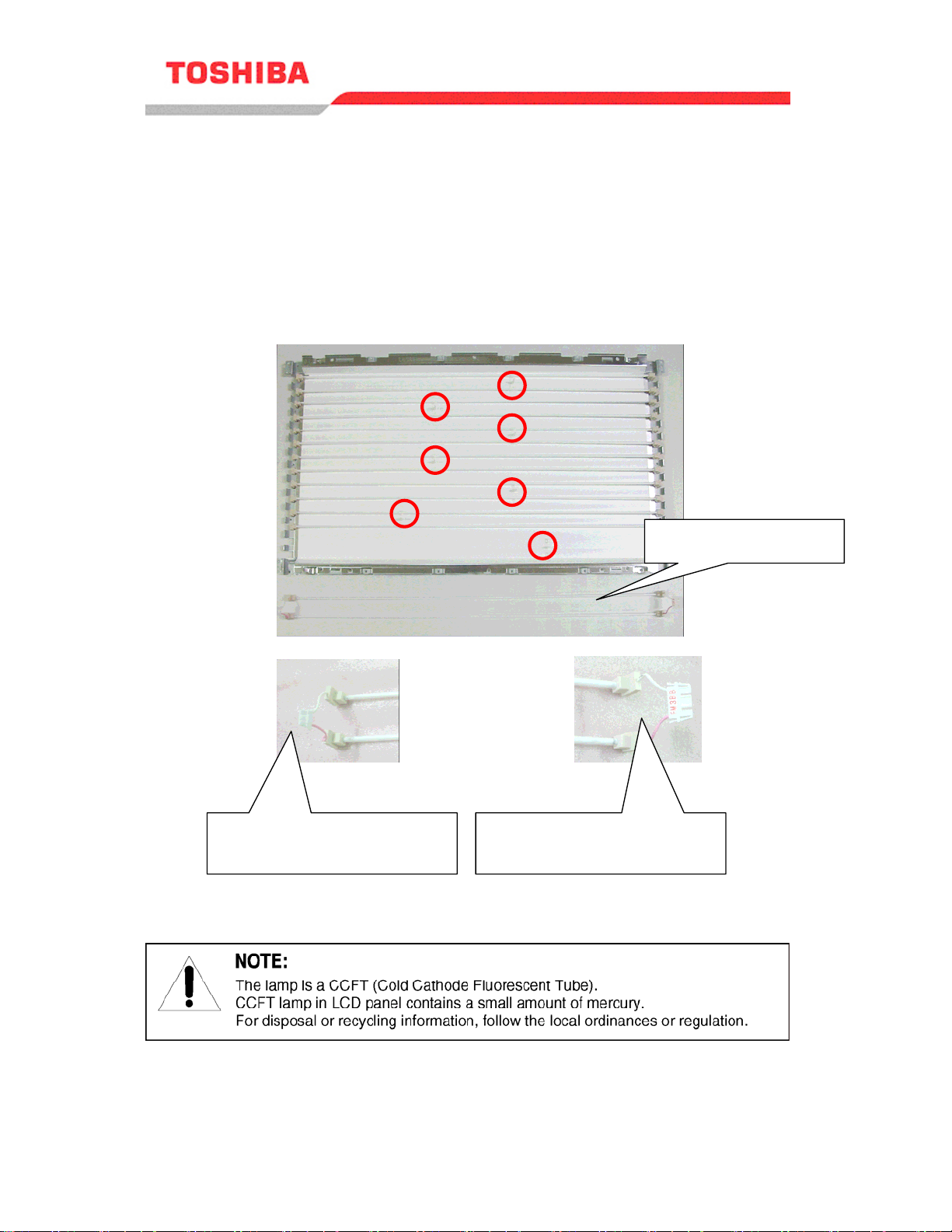
5. Replacing Lamp Units
5-1. Remove the old lamp units from the lamp clip, and replace them with new ones.
Be very careful not to break the lamp units when detaching/reattaching them. Keep
dust off the units.
Note: The seven lamp direct illumination system uses 14 CCFTs
(Cold Cathode Fluorescent Tubes) to provide backlighting for
the LCD display.
One lamp unit consists
of two lamps.
Small connector
Connected to INV board
(GND side)
Large connector
Connected to INV board
(HOT side)
Service Instruction
2004 LCD Television
Page 5 of 12

6. Assembly
6-1. Follow the lamp unit removal instructions in reverse order to re-assemble
the backlight lamp assembly. (Section2-5).
Assembly Cautions
Handle fragile lamp units with extreme caution.
Replace lamp units in a dust-free environment.
Do not bend or pinch flat cables when installing the panel unit.
Ferrite core may be damaged even by a slight shock. Attach ferrite cores
very carefully.
Connect the connectors securely to the INV board.
Connect small connectors
to the INV board (HOT
side).
Connect small connectors
to the INV board (GND
side).
INV board (HOT side)
INV board (GND side)
Panel unit
Flat cables
Service Instruction
2004 LCD Television
Page 6 of 12

Model: 32HL84, 32WL46B/G/C/A/E/R/T
1. Cautions for Backlight Lamp Unit Replacement
The backlight lamps used in the listed Liquid Crystal Display (LCD) modules are
consumables. Follow the included replacement procedures when replacing these
components.
Disconnect AC power before starting the replacement procedure. The high
voltage applied to the backlight lamps produces an electrical shock hazard if
caution is not used when servicing this area.
Backlight lamp units are fragile and caution should be used when handling.
Ferrite cores are attached to the backlight lamp units with double-sided adhesive
tape. Use caution when removing these ferrite cores, as excessive force may
cause damage.
Where possible, replace backlight lamp units in a clean and dust-free environment.
TFT-LCD Module Bottom view
Return FFC
INV board
(HOT) side
INV board
(GND) side
C board
C board cover
Flat cables
Ferrite cores
Service Instruction
2004 LCD Television
Page 7 of 12

2. Removing C Board Cover and C Board
2.1. Remove the two screws securing the C board cover.
2-2. Remove the two screws securing the C board. Remove the C board and
connectors, using caution to remove the ferrite cores.
Use caution when removing the ferrite
cores, as excessive force may cause
damage.
Service Instruction
2004 LCD Television
Page 8 of 12

3. Removing INV Cover and INV Board (HOT Side / GND Side)
3-1. Remove the return FFC connected to the INV board.
3-2. Remove the four screws securing the INV cover.
3-3. Disconnec t the eight lamp unit connectors from and remove the four s crews
securing the INV board (HOT side).
3-4. Disconnec t the eight lamp unit connectors from and remove the six screws
securing the INV board (GND side).
Service Instruction
2004 LCD Television
Page 9 of 12

4. Removing Panel Unit and Lamp Holder
4-1. Remove the 22 screws securing the panel unit.
4-2. Remove the six screws securing the lamp holder.
Service Instruction
2004 LCD Television
Page 10 of 12

5. Replacing Lamp Units
5-1. Remove the old lamp units from the lamp clip, and replace them with new ones.
Be very careful not to break the lamp units when detaching/reattaching them. Keep
dust off the units.
Note: The eight lamp direct illumination system uses 16 CCFTs
(Cold Cathode Fluorescent Tubes) to provide backlighting for
the LCD display.
Lamp unit consis t s
of two lamps
Small connector
Connected to INV board
(GND side)
Large connector
Connected to INV board (HOT side)
Service Instruction
2004 LCD Television
Page 1 1 of 12

6. Assembly
6-1. Follow the lamp unit removal instructions in reverse order to re-assemble
the backlight lamp assembly. (Section2-5).
Assembly Cautions
Handle fragile lamp units with extreme caution.
Replace lamp units in a dust-free environment.
Do not bend or pinch flat cables when installing the panel unit.
Ferrite core may be damaged even by a slight shock. Attach ferrite cores
Connect the connectors securely to the INV board.
Connect large connectors to
the INV board (HOT side).
very carefully.
Connect small connectors to
the INV board (GND side).
INV board (HOT side)
INV board (GND side)
Panel unit
Flat cables
Service Instruction
2004 LCD Television
Page 12 of 12

SCHEMATIC DIAGRAM
MODEL : 26HL84
WARNING: BEFORE SERVICING THIS CHASSIS, READ THE "X-RAY RADIATION PRECAUTION", "SAFETY
PRECAUTION" AND "PRODUCT SAFETY NOTICE" ON THE MANUAL FOR THIS MODEL.
CAUTION: The international hazard symbols " " in the schematic diagram and the parts list designate components
which have special characteristics important for safety and should be replaced only with types identical to those in the
original circuit or specified in the parts list. The mounting position of replacements is to be identical with originals.
Before replacing any of these components, read carefully the PRODUCT SAFETY NOTICE on the MANUAL for this
model. Do not degrade the safety of the receiver through improper servicing.
NOTE:
1. RESISTOR Resistance is shown in ohm [K = 1.000, M = 1.000.000]. All resistors are 1/6W and 5% tolerance
2. CAPACITOR Unless otherwise noted in schematic, all capacitor values less than 1 are expressed in
carbon resistor, unless otherwise noted as the following marks.
1/2R = Metal or Metal oxide of 1/2 watt 1/2S = Carbon compsistion of 1/2 watt
1RF = Fuse resistor of 1 watt 10W = Cement of 10 watt
±10% G = ±2% F = ±1%
K =
µ
the values more than 1 in pF.
All capacitors are ceramic 50V, unless otherwise noted as the following marks.
Electolytic capacitor Mylar capacitor
F, and
3. The parts indicated with "
4. Voltages read with DIGITAL MULTI-METER from point indicated to chassing ground, using a color bar signal with
all controls at normal, line voltage at 220 volts.
5. Waveforms are taken receiving color bar signal with enough sensitivity.
6. Voltage reading shown are nominal values and may vary
" have special characteristics, and should be replaced with identical parts only.
±20% except H.V.
– 55 –

SCHEMATIC DIAGRAM STRUCTURE:
– SIGNAL Circuit CONNECTOR [ SHEET– 1/7 ] .................. 1/57
– AV [ SHEET– 2/7 ] .................. 2/57
– TERMINAL [ SHEET– 3/7 ] .................. 3/57
– COLOR DIFFERENCE SWITCHING [ SHEET– 4/7 ] .................. 4/57
– V/C [ SHEET– 5/7 ] .................. 5/57
– HDMI_VARI [ SHEET– 6/7 ] .................. 6/57
– Audio-MUTE [ SHEET– 7/7 ] .................. 7/57
– TN-AOUT Circuit CONNECTOR [ SHEET– 1/8 ] .................. 8/57
– TIF & MA [ SHEET– 2/8 ] .................. 9/57
– IMA MOPULE [ SHEET– 3/8 ] ................ 10/57
– A-OUT [ SHEET– 4/8 ] ................ 11/57
– HP-AMP [ SHEET– 5/8 ] ................ 12/57
– TEMP SENSOR [ SHEET– 6/8 ] ................ 13/57
– LipSync DIGITAL PART [ SHEET– 7/8 ] ................ 14/57
– LipSync ANALOG PART [ SHEET– 8/8 ] ................ 15/57
– CONT Circuit KEY [ SHEET– 1/2 ] ....................................................... 16/57
– POWER SW [ SHEET– 2/2 ] .......................................................17/57
– DATA_REWRITE Circuit ............................................................................................................... 18/57
– FRONT-AV Circuit AV-1 [ SHEET– 1/2 ] ................................................................... 19/57
– AV-2 [ SHEET– 2/2 ] ................................................................... 20/57
– IR-PASS/RMT/LED Circuit ............................................................................................................ 21/57
– SCALER Circuit DIGITAL INPUT [ SHEET– 1/36 ] .............. 22/57
– CAPTURE INPUT [ SHEET– 2/36 ] .............. 23/57
– MEMORY CONNECTION [ SHEET– 3/36 ] .............. 24/57
– PLL [ SHEET– 4/36 ] .............. 25/57
– OSD [ SHEET– 5/36 ] .............. 26/57
– IIC [ SHEET– 6/36 ] .............. 27/57
– US OSD SYNC GENERATOR [ SHEET– 7/36 ] .............. 28/57
– POWER [ SHEET– 8/36 ] .............. 29/57
– SUB MICOM (1) [ SHEET– 9/36 ] .............. 30/57
– SUB MICOM (2) [ SHEET– 10/36 ] ............ 31/57
– SUB MICOM (3) [ SHEET– 11/36 ] ............ 32/57
– LVDS OUT [ SHEET– 12/36 ] ............ 33/57
– POWER CONNECTOR AND DIMMING [ SHEET– 13/36 ] ............ 34/57
CONNECTOR BETWEEN SIGNAL BOARD
–
– EMI FIL 2 [ SHEET– 15/36 ] ............ 36/57
– LVDS POWER AND OTHERS [ SHEET– 16/36 ] ............ 37/57
– LVDS OUT (SHARP LCD) [ SHEET– 17/36 ] ............ 38/57
– CONNECTOR [ SHEET– 18/36 ] ............ 39/57
– 3CHADC1_LPF [ SHEET– 19/36 ] ............ 40/57
– 3CHADC2_LPF [ SHEET– 20/36 ] ............ 41/57
– DVCD_LPF [ SHEET– 21/36 ] ............ 42/57
– 3CHADC HD/VD [ SHEET– 22/36 ] ............ 43/57
– 3CHADC1 [ SHEET– 23/36 ] ............ 44/57
– 3CHADC2 [ SHEET– 24/36 ] ............ 45/57
– DVCD TC90A92AFG [ SHEET– 25/36 ] ............ 46/57
– DVCD_POWER [ SHEET– 26/36 ] ............ 47/57
– GENESIS-1 [ SHEET– 27/36 ] ............ 48/57
– GENESIS-2 [ SHEET– 28/36 ] ............ 49/57
– SDRAM [ SHEET– 29/36 ] ............ 50/57
– GENESIS_POWER [ SHEET– 30/36 ] ............ 51/57
– GENESIS_CPU [ SHEET– 31/36 ] ............ 52/57
– OSD MICON 1/4 [ SHEET– 32/36 ] ............ 53/57
– OSD MICON 2/4 [ SHEET– 33/36 ] ............ 54/57
– OSD MICON 3/4 [ SHEET– 34/36 ] ............ 55/57
– OSD MICON 4/4 [ SHEET– 35/36 ] ............ 56/57
– DC/DC CONVERTER [ SHEET– 36/36 ] ............ 57/57
[ SHEET– 14/36 ] ............ 35/57
– 56 –

CIRCUIT BLOCK DIAGRAM
E1
E2
E3
CS_E4
CS_E5
DVI
AV
QV01
CXA2069Q
CS
QV254
MM1519XQ
V_AV_MC SYNC_M
V_AV
C_AV
V_PIP
SYNC_S
C_AV_SUB
Y1
SUB-Y
COMB
QY100
TC90A45F
Y_COMB_S
C_COMB_S
SUB CD
QY501
TA1340F
HD
VD
G-HYPER
DVCD
QZ501
TC90A92
A/D
QU100
A/D
QX100
I/P
QX300
GM6010
A PORT B PORT
NORMAL CS CVBS
D/W SUB MAIN
YPbPr1
CVBS/Y
C
YPbPr2
CTRL
YPbPr1
CVBS/Y
PJ15A
YPbPr2
PJ13A
C
MST9883M
TC90A92AFG
42MHz
3ch A/D
MST9883M
CTRL
3ch A/D
YCbCr
16
I2C
TV MICRO
MN102HF75KBF
EEPROM
Y/C
8
24
I2C
64Kbit
2M x 32Mbit
SDRAM
256Kbit
EEPROM
RGB
4:2:2
G-Hyper MICRO
TMPA8700CSF
ADC08060
ADC08060
ADC08060
RGB
5:6:5
1M x 32bit
DDR-SDRAM
133MHz
TC90A94TBgm6015
I2C
BEP MICRO
M30626FHPGP
128Kbit
EEPROM
RGB 8:8:8
50/60Hz,OS_ON/OFF
THC63LV
DM83R
MK1707STR
133MHz
ICS487G-35T
13.5MHz
TEMP
BL_ON/OFF,DIM
PJ100
LVDS
PJ12 PJ101
PJ102
– 53 – – 54 –

L_VARIOUT
R_VARIOUT
L_MONI
R_MONI
GND_V_MONI
V_MONI
FRONT-AV(AV-2)
L_VARI
R_VARI
GND(1mm)
RESET_IMA
R_AV
GND(1mm)
R_TV
TV-GND(0.75mm)
TV_V_GND
V_TV
AOUT
TV2V
MUTE_AUDIO
DET_FAULT
DET_HP
MUTE_SPK
GND
GND
GND
GND
GND
GND
TUNER-AOUT
3.3VA
3.3VA
12V
12V
SCL1
SDA1
HDMI
from
PC Input
9P-BB
PV22A
1
2
3
GND
4
GND
5
6
7
GND
8
9
SOCKET B-B 9P
19P-BB
P103B
1
2
3
4
NC
5
6
7
L_AV
8
9
AFT1
10
11
L_TV
12
13
14
15
AFT2
16
GND
17
18
GND
19
SOCKET-B-B 19P
23P-BB
P104A
MUTE_AUDIO
1
2
3
4
5
6
7
8
9
10
11
5V2
12
5V2
13
5V2
14
32V
15
9V
16
9V
17
9V
18
19
20
21
22
23
SOCKET B-B 23P
3P
PS01
KETSU
R
1
GND
2
L
3
3P
3
GND
L_PC 2
1
R_PC
P612A
KETSU
L_VARIOUT
R_VARIOUT
GND
GND
L_MONI
R_MONI
GND
GND_V_MONI
V_MONI
L_VARI
R_VARI
RESET_IMA
R_AV
L_AV
GND_TV
A_TV2
GND_TV2
V_TV2
DET_FAULT
MUTE_SPK
GND
GND
GND
GND
GND
GND
SCL1
SDA1
R_HDMI
TLB016 TLB018TLB017
GND
L_PC
R_PC
GND
GND
AFT1
R_TV
L_TV
GND
V_TV
AFT2
GND
L_HDMI
5V2
9V
3.3VA
12V
GND
GND
L_PC
R_PC
L_VARIOUT
R_VARIOUT
GND
GND
L_MONI
R_MONI
GND
GND_V_MONI
V_MONI
L_VARI
R_VARI
GND
RESET_IMA
R_AV
L_AV
GND
R_TV
L_TV
GND
GND_TV
V_TV
GND
A_TV2
GND_TV2
V_TV2
MUTE_AUDIO
DET_FAULT
MUTE_SPK
GND
GND
GND
GND
GND
GND
SCL1
SDA1
5-C8
R_HDMI
GND
L_HDMI
5-C8
2-E2
TO DVI
6-A1
6-A1
2-E2
ACDETECT
7-B1
6P_2.5mm_1.5A
GND
KEY_1
PV15
GND
KEY_2
3.3V
GND
GND
CS2-DVI(NC)
PJ15A
25FMN-BTK-A
GND
NC
POWER_SIG
GND
NC
DVI-RST
5V_ANALOG
654321
GND
GND
HD_CD_SUB
312HD4
GND
GND
GR90
OPEN
GR91
SHORT
5-B8
5-B8
VD_CD_SUB
HD_CD_SUB
VD_CD_SUB
TLB209 TLB204TLB207
576
VD
GND
5-C8
GND
GND
GND
ACDETECT
40 39 38 37 36 35 34 33 32 31 30 29 28 27 26 25 24 23 22 20 19 18 17 16 15 14 13 12 11 10 9 8 7 6 5 4 3 2 1
GND
GND
GND
GND
GND
RMT_IN
KEY_1
KEY_2
NC(YS_TEXT)
POWER_SIG
GND
NC(SM_TX)
ACDETECT
NC(SM_RX)
SCL
SCL1
DVI_RST
PK91
OPEN
5-B8
CR_CD_SUB
CR_CD_SUB
89
Pr(2),R
GND
STOP_FAN
STOP_FAN
SDA
SDA1
5-C8
TLB202
CB_CD_SUB
Pb(2),B
POWER_LCD
NC
TO HDMI
3.3V
5V_DIGITAL
3412
3.3V
C927
1k
R929
+
C928
5-B8
CB_CD_SUB
TLB198TLB210 TLB206TLB208
Y_CD_SUB
TLB200
10
Y(2),G
GND
5-B8
KVD
KVD
KVD
POWER_LCD
9V_ANALOG
5V_ANALOG
GND_ANALOG
GND_DIGITAL
5
0.1uF
OPEN
5-B8
Y_CD_SUB
2-A8
SYNC_M
SYNC_M
HDMI_RST
7986
PV16
OPEN
DE99
RK34 LF-A4
5V1
1
Q922
3
Reset
2
PST994D
PB1
PR1
GND_Y1
GND_PB1
GND_PR1
GND_PR1
TLB194 TLB190 TLB150TLB179TLB182 TLB160 TLB156TLB170
13 151411 12
GND
GND
HD(1)
VD(1)
7-B1
2-C6
MUTE_E
V_PIP_MC
MUTE_E
V_AV_MC
V_PIP_MC
PR1
16 17
Pr(1)
2-B6
V_AV_MC
GND_PB1
GND
PB1
TLB187TLB192
18 19
Pb(1)
POWER_TV
GND_Y1
GND
SPM
7-B1
SPM
Y1
TLB184
2
0
Y(1)
MUTE_A
Y1
GND_C
C_AV
GND_C
TLB180
GND
C
7-B1
2-B8
SYNC_S
MUTE_A
SYNC_S
GRV13
SHORT
GRV14
SHORT
C_AV
GJ128
RM73B1HR00OD
GND
GND
GND
5-C8
10P±2.5mm±1.5A±Beige
243252221 2
Y
21
SPM
MUTE_E
SYNC_M
RMT_OUT
V_PIP_MC
V_AV_MC
ACP
LED
POWER_TV
MUTE_A
SYNC_S
GND
VD_OSD
HD_OSD
SCALER
V_AV
GND_V
GND
SCL1
SCL1
5-C8
SDA1
SDA1
P811A
GND
GND
POWER_FAN
GND(MICOM)
5V1
234567
1
GND
5V1
7-B1
AFT1
AFT2
AFT1
AFT2
HYP_RST
POWER
32V
12V
GND(MICOM)
GND(MICOM)
25V0.1
C524
TLB169 TLB162 TLB153 TLB147TLB158TLB166TLB178
21
PJ14A
GND
GND
9V
13P_2.5mm_1.5A_Beige
SCALERSCALER
PJ13A
CONNECTOR FFC 0.5mm 40P
RESET
3.3VA
3.3VA
8910
TLB168
4
GND
GND(MICOM)
STOP_FAN
++
CV81
16V470
CV79
16V470
25V0.1
C523
TLB164
635
3.3VA
3.3VA
GND
POWER_SIG
1
3.3VA
ACDETECT
3
2
GR289
KETSU
25V0.1
C522
978
GND
GND
POWER_LCD
POWER_TV
4
5
L289
TLN3299D
1110
5V2
5V2
9V
GND(5V2)
GND(5V2)
6
8
9V
GND
++
CV82 CV80
10V1000 10V1000
1312
GND
9V
9
5-D8
5V2
GND(5V2)
GND(5V2)
10 12117
NC
5V2
P810A
13
13P_2.5mm_1.5A_Beige
5V2
19P-FFC
STOP_FAN
R_HDMI-m
L_HDMI-m
GND
GND
2-D2
R_HDMI-DVI
L_HDMI-DVI
2-D2
SY_E3_GND
2-F1
SY_E3
SC_E3_GND
2-F1
SC_E3
SSW_E3
2-F1
V_E3_GND
V_E3
GND
L_E3
R_E3
GND
R_HDMI-m
L_HDMI-m
GND
GND
R_HDMI-DVI
L_HDMI-DVI
SY_E3_GND
SY_E3
SC_E3_GND
SC_E3
SSW_E3
V_E3_GND
V_E3
GND
L_E3
R_E3
GND
PV23B
19FMN-BTK-A
1
2
3
4
5
6
7
TLC0182
TLB0161
8
TLB0162
9
TLB0163
10
TLB0164
11
TLB0165
12
TLB0166
13
TLB0167
14
TLB0168
15
TLB0169
16
TLB0170
17
TLB0171
18
19
R_HDMI-m
L_HDMI-m
GND
DET_HP
GND
R_DVI
L_DVI
E3_Y_GND
SY_E3
E3_C_GND
SC_E3
SW_E3
V_E3_GND
V_E3
GND(E3_Audio)
L_E3
R_E3
TUNER-GND
(2mm)
FRONT-AV(AV-1)
RI_IN
RI_OUT
GND
RI_IN
GND
GND
GND
RI_OUT
GND
98
534 7612
CONNETOR
PB22A
9P_2.5mm
IR-IN
GND
IR-OUT
GND
LED
5V1
REM IN
GND
REM OUT
IR-PASS
6P
PA0 5A
6P_2.5mm_1.5A
TLB199
5V11
NC
2
GND
TLB0136
P518B P520
1P
TLB0143
GND
1P
GND
TLB0181
3
KEY_1
4
KEY GND
TLB0183
5
KEY_2
6
TUNER_GND
PA0 6A
3P_2.5mm_1.5A_Beige
TLB227
RA80
1
KEY_1
RM73B1HR00OD
TLB228
2
KEY GND
NC3
to KEY BOARD
to PA01
to POWER-SW BOARD
to PA06B
KEY
GND(TUNER)
26/32HL84
26HL84
SIGNAL (CONNECTOR)
SIGNAL (CONNECTOR)
SHEET-1/7
(1/57)

LV74
RV98
LV75
KETSU
L_HDMI-DVI
R_HDMI-DVI
V_E3_GND
TEM2121M
SY_E3_GND
TLB009
RV99
RV100
RM73B1HR00OD
KETSU
LV04
RM73B1HR00OD
RM73B1HR00OD
RV101
LV02
KETSU
GRV84
RM73B1HR00OD
RM73B1HR00OD
L_HDMI-DVI
R_HDMI-DVI
GRV86
GRV85
RM73B1HR00OD
GND
V_TV_A
GND
L_TV
R_TV
A_TV2
GND
V_TV2_A
SSW_E1
SY_E1
GND
SC_E1
GND
SSW_E2
GND
SY_E2
GND
SC_E2
GND
V_E1
GND
L_E1
R_E1
GND
V_E2
GND
L_E2
R_E2
GND
R_E5
L_E5
GND
R_E4
L_E4
GND
CS27
B2.2u
RM73B1HR00OD
GRV89
RM73B1HR00OD
CS26
B2.2u
GRV87
GRV88
R_E5
L_E5
VC_E3
Y_E3
C_E3
SSW_E1
SSW_E2
V_E1
CS16
B2.2u
CS15
B2.2u
1-A1
R_E3
L_E3
GND
RM73B1HR00OD
RM73B1HR00OD
GND
LV03
KETSU
SC_E3_GND
GND
SSW_E3
SY_E1
GND
SC_E1
GND
GND
SY_E2
GND
SC_E2
GND
GND
L_E1
R_E1
V_E2
GND
L_E2
R_E2
GND
TLC334
RS26
TLC335
100
RS25
100
R_E4
L_E4
GND
RS17
100
RS18
100
GND_V_MONI
TLC336
L_MONI
R_MONI
TLC337
RS37
100K
RS35
RS45
10k
TLC338
RS46
+
CS25
10k
7L16V100u
L_MONI
R_MONI
TLC342
47k
RS47
47k
RS48
TLC340
TLC343
L_SEL
TLC345
100K
RS38
RS39
100K
TLC346
TLC341
47k
RS49
RS50
100K
SEL_IN_B
SEL_IN_A
SEL_OUT_A
SEL_OUT_B
LOUT2
GND
V_MONI
LV05
V_MONI
KETSU
GRV91
GRV90
RM73B1HR00OD
CV64 RV66
16V470
TLC339
LV1 3
TRF4100AT
RM73B1HR00OD
TLC071
+
CV65
7L16V100u
+
CV66
F0.1
QV12 should be laid closeby Monitor output teaminals.
R_PC
GND
L_PC
QS05
9.1
X2
15 161210911 1413
4.3
X1
4.3
X-OUT
4.3
X0X3Y1
4.3
8.9
A
0
B
(to A/V-IC)
QS06
9.1
4.3
X2
15 161210911 1413
4.3
X1
4.3
X-OUT
4.3
X0X3Y1
4.3
47k
0
A
0
B
(to FIX-OUT)
RV62
100
TLC347
TLC348
TLC349
R_PC
L_PC
CS28
OPEN
RS23
OPEN
CD4052BNSR
Y-OUT
INH
VEE
VSS
CD4052BNSR
Y-OUT
INH
VEE
VSS
0
123
4.7
QV12
MM1505XRE
9.1
Y0VDD
Y2
Y3
Y0VDD
Y2
Y3
4.4
1264587 3
4.5
4.4
4.5
0
0
0
4.3
1264587 3
4.2
4.3
4.3
4.3
0
0
0
TLC072
QS07
2SC3326B
TLC350
TLC351
4.7
0
4.7
CS29
OPEN
RS24
OPEN
R_SEL
RS40
100K
ROUT2
TLC074 TLC077 TLC081
RS34
TLC073
47K
QS08
2SC3326B
RS33
47K
RV61
546
CV68
F0.1
KETSU
GND_TV
V_TV
GND
L_TV
R_TV
A_TV2
GND_TV2
V_TV2
1-B7
1-B7
GND
R_E3
L_E3
V_E3_GND
V_E3
EXT-3
V_E3
(FRONT)
SY_E3
SY_E3_GND
SY_E3
SC_E3_GND
SC_E3
SSW_E3
GV12
GV13
TEM2121M
TLB005
5V2
9V
9V
5-D8
RV60
CV07
25V0.1
4.2
VGND
S2-4
RV41
100
TLC141 TLC151TLC144
YOUT 1
TRAP1
S-4
4.4
TLC143
L_SEL
TLC148
CC21
R_AV
RS12 RS11
100 100
4.5
4.5
VOUT1
LOUT1
ROUT1
COUT2
TRAP2
ROUT2
V/YOUT2
LOUT2
VOUT3
ROUT3
YOUT 3
LOUT3
COUT3
DC OUT
SCL
4.0
4.4
TLC145
CV47
CS11 RS13
10V1u 4.7K
RV30
TLC147
MY_MC
2.2k
OPEN
RV70
100
GJ30
OPEN
CIN1
BIAS
YIN1
MUTE
Vcc
AGND
SDA
RV5V5LV5
TLC149TLC142
B10V1u
TLC150
100
R_SELe
QV06
2SA1576A
TLC367
TLC152
RV73
2.2k
GND
L_AV
TLC153
4.5
CV10
5150494847464544434241403938373533
4.5
TLC156
7L16V10u
+
TLC157
4.9
CV09
B10V1u
4.4
CS31
4.5
B2.2u
4.4
4.5
CS30
9.1
B2.2u
3.7
TLC158
0
3634
0
TLC154
3.2
RV10
100
3.5
TLC155
RV09
ADR
100
0
323130292827262524
330
RS14
CS12
10V1u
GND
10V1u
CS01
RS01
4.4
4.4
100 B10V1u
5.6k
RV6V6LV6
232221
L_E4
V_TV2_A
TLC132
CV46
10V1u
CS23
TLC133
CC20
5.3
4.4
QV01
4.4
CS09 RS09
10V1u 5.6k
GND
A_TV2
TLC134
RS51
2.7k
TLC135
CS24
B10V1u
10V1u
TLC136
TLC139
OPEN
0
4.3
COUT1
C4
RV4Y4LV4
TLC137TLC130
TLC138TLC131 TLC146
CS10 RS10
10V1u 5.6k
R_E4
L_TV
R_TV
V_TV_A
CS02
10V1u
TLC122
TLC125
TLC120
CV02
B10V1u
5.6k
RS02
CC78
100p
CC13
OPEN
TLC126
TLC123
TLC121
CC77
64636261605958575655545352
5.3
4.4
4.4
100p
CV01
RV01
B10V1u
TLC097
V_E1
100
TLC082
CS03
L_E1
10V1u
TLC098
TLC083
CV03
RV03
SY_E1
R_E1
SC_E1
SSW_E1
V_E2
L_E2
SY_E2
R_E2
SC_E2
SSW_E2
VC_E3
L_E3
Y_E3
R_E3
C_E3
SSW_E3
R_SEL
CS51
16V4.7u
GND
RS42
100K
RS41
100K
RS44
100K
B10V1u
100
TLC099
TLC084
CS04
10V1u
TLC093
TLC085
CV04
25V0.1
RV06
TLC094
100
MA8091-L
1k
RV07
TLC100
CV05
RV08
B10V1u
100
TLC101
CS05
10V1u
TLC102
CV11
RV11
B10V1u
100
TLC103
CS06
10V1u
TLC104
CV13
TLC095
25V0.1
100
RV12
RV14
5.6k
TLC105
TLC086
RV15
CV14
100
B10V1u
TLC092
TLC106
TLC088
RV17
CV06
B10V1u
TLC107
TLC096
100
RV19
CV15
25V0.1
RS53
47K
RS52
1.8K
RS54
56K
4.4
TLC359
RS03
4.4
5.6k
TLC117
DV01
4.0
OPEN
TLC358
RS04
4.4
TLC118
5.6k
DV03
4.4
MA8091-L
TLC360
DV05
DV07
MA8068-M
4.8
TLC108
4.0
TLC109
RS05
4.4
TLC110
5.6k
DV09
4.0
OPEN
TLC111
RS06
4.4
TLC112
5.6k
DV10
4.4
MA8091-L
TLC361
DV11
MA8091-L
4.8
DV14
TLC357
MA8068-M
4.0
TLC113
4.4
TLC114
RS07CS07
DV15
4.0
OPEN
5.6k10V1u
TLC115
4.4
TLC116
RS08CS08
DV02
4.4
5.6k10V1u
MA8091-L
TLC362
19181716151413121110987654321
DV19
MA8091-L
RV21
100
QS15
2SC4081-Q
RS36
4.7K
R_SELe
V1
LTV
LV1
RTV TV
Y1
RV1
C1
S2-1
S-1
V2
LV2
CXA2069Q
Y2
RV2
C2
S2-2
S2
V3
LV3
Y3
RV3
S2-3
S-3
C3
V4
4.7
3.9
20
TLC127
TLC364
CV45
TLC128
DV21
MA8068-M
RV20
TLC129
SY_MC
QV70
2SC4081-Q
RS16
TLC372TLC369
100
TLC373TLC370
RS15
100
TLC375
CV12
F0.1
VIDEO_G
R_AV
L_AV
TLC161
+
LV72
KETSU
V_MON
LV73
KETSU
7L16V100
CV40
7L16V100u
RV90
10u COLTRF4100AT
CV08
RV87
R_AV
L_AV
GND
RV88
RV89
CV42
F0.1 TRG4100AT
+
RV79
2.7k
RM73B1HR00OD
TLC377
RM73B1HR00OD
RM73B1HR00OD
RM73B1HR00OD
LV0 9
RV27
RV77
100
MY_MC
SY_MC
100
RV28
KETSU
TLC378
RV78
GND_V
C_AV
GND_C
RV29
1/2R100
RV76
2.7k
TLC379
100
2SA1576A
V_AV
2SA1576A
TLC380
4-B2
4-B2
LV42
QV73
TLC164TLC163
TLC165TLC162
RV26
560
QV09
QV72
2SA1576A
ROUT2
LOUT2
GND_V
GND_C
P4
VSS
10
4.7
TLC387
RB37
330
TLC167 TLC169
1M
RB43
330
1M
11
P5
P3
4.7
7
CB41
B2200
RB40
3.9k
TLC171 TLC173
QB44
RB38
2SA1576A
RB39
12k
CB46
B2200
TLC170TLC168
RB44
TLC388
12
0
P6
P2
P1
4.7
6
5
2SA1576A
RS63
1k
P7
RB46
3.9k
TLC172 TLC174
QB46
RB45
12k
100
100
RS62
RS61
13
14
15
16
3.5
3.2
5.2
SCL
SDA
VDDA0
VDAC
P0
A2
A1
0
0
5.2
5.2
1
4
3
2
10V1
CB40
10V1
CB45
V_AV_MC
V_AV_MC
TLC166
+
CV24
F0.1
CV23
7L16V100u
SDA1
SCL1
SEL_IN_A
SEL_IN_B
SEL_OUT_A
SEL_OUT_B
QS14
RN1404
LV01
KETSU
V_PIP_MC
TLC382
QS13
RN1404
RJ40
TLC383
RM73B1HR00OD
RM73B1HR00OD
RJ41
C_AV_SUB
QS12
RN1404
V_PIP
GND_PIP
C_AV_SUB
GND
1-F3
V_PIP_MC
RS75
220K
QS10
JLC1562BFEL
ADD:W 76H
R 77H
QS11
RN1404
TLC385
RS74
5-B1
1k
9
0
0
8
TLC386
RB42
TLC177
10k
TLC391
CB43
B3300
CV48
B3300
SYNC_M
SYNC_M
QB45
TLC175
2SC5343UF-Y
RB48
10k
TLC176
TLC178
DV25
KETSU
QB47
2SC5343UF-Y
DET_FAULT
RV141
KETSU
TLC392
+
DET_FAULT
RESET_IMA
SDA1
SCL1
CV69
KETSU
QV20
KETSU
1-D15-D1
1-C1
CB42
CH560
RB41
3.9k
CB47
CH560
RB47
3.9k
RS76
5.6k
RS57
5.6k
RS58
5.6k
RS59
5.6k
RS60
5.6k
A_MUTE
TLB028
TLB027
RV91
V_TV2_A
100
QV13
TLC368
CV78
KETSU
CV73
2SC4081-Q
25V0.1
1k
RV92
QV14
KETSU
TLC376
TLC371
RV96
KETSU
KETSU
RV94
2.2k
RV95
RS64
RS66
39k
RS19
39k
100
CS14
V_MON
NP
16V4.7u
TLC080
TLC078
RS21
2.2k
CS13
RS22
2.2k
TLC079
QS09
RN2404
TLC090
QS04
2SC4081-Q
RS20
100
RS67 RS65
56k 56k
TLC091
RS56
100k
CS21
16V4.7u
CS22
16V4.7u
RS55
10k
CS20
B16V0.47
TLC363
P120
OPEN
GEMSTAR EPG
QS03
2SC4081-Q
TLC076TLC075
RS30
16V4.7u
1k
RS29
1k
TLC354TLC352
CV67
100
16V10
132
RV93
47
RV97
KETSU
4
TLB026
VIDEO_G
26/32HL84
26HL84
SIGNAL (AV)
SIGNAL (AV)
SHEET-2/7
SYNC_S
V_AV
GND_V
C_AV
GND_C
SYNC_S
2.0Vp-p
1-F4
(2/57)

For Lightning
EXT-1
R
EXT-2
EXT1-S
EXT2-S
Y/C Socket SW
L
R
Y
CB
EXT-4
CR
\U+2550ÅP\U+2550\U+00D9\U+2550\U+00D0
\U+2550ÅP\U+2550\U+00D9\U+2550\U+00D0
\U+2550ÅP\U+2550\U+00D9\U+2550\U+00D0
\U+2550ÅP\U+2550\U+00D9\U+2550\U+00D0
to TUNER
V
R2
L
M2
L2
V
R1
L
M1
R
L1
PV01
JACK 6P
PV02
M2
L2
R1
M1
L1
PV03
JACK 5P
P515B
INSERT-PIN
GND
PR80
LGA6502-0101
TLB236
TLB235
TLB234
TLB233
TLB231
TLB230
MA111-(TX)
1SS3551SS355
TLB232
RB76
KETSU
DB76DB90
TLB80
TLB79
MA111-(TX)
RV368
RM73B1HR00OD
RV369
RM73B1HR00OD
RV370
RM73B1HR00OD
RV371
RM73B1HR00OD
RI_OUT
GND
RI_IN
GND
LV282
KETSU
RI_OUT
GND
RI_IN
GND
GND_E4
CR_E4
GND_E4
CB_E4
GND_E4
Y_E4
SYE1
C
Y
RV33
1/8W75
RV34
1/8W75
R266
R265
R264
RV35
1/8W75
RV40
1/8W75
RC03
1/8W75
RC02
RC04
C
Y
A
CV38
LV37
1000
OPEN
RV37
1/8W75
RC01
680
680
B1000p
CV39
1000
680
680
B1000p
1/8W75
1/8W75
RC06
680
RC05
680
L_E1
L_E1
R_E1
OPEN
CC04
CC06
B1000p
R_E1
GND
L_E2
L_E2
R_E2
R_E2
GND
R_E4
R_E4
L_E4
L_E4
GND
CC02
B1000p
CC01
A
LV38
RV36
1/8W75
B1000p
CC03
CC05
B1000p
GND
SC_E1
GND
SSW_E1
V_E1
GND
SY_E2
SY_E2
GND
SC_E2
SC_E2
GND
SSW_E2
SSW_E2
V_E2
V_E2
GND
GND
RB90
KETSU
CC99
50V1000p
M
(RI-GND) (AV-GND)
EXT-5
RV372
RM73B1HR00OD
1/8W75
L
M2
R
L2
R1
Y
CB
M1
CR
L1
PV04
JACK 5P
R288
1/8W75
R287
R286
1/8W75
RC08
TLC063
680
R_E5
R_E5
CC07
TLC061
B1000p
L_E5
L_E5
CC08
RC07
B1000p
680
GND
RV373
RM73B1HR00OD
RV374
RM73B1HR00OD
RV375
RM73B1HR00OD
LV283
KETSU
GND_E5
CR_E5
GND_E5
CB_E5
GND_E5
Y_E5
26/32HL84
SIGNAL (TERMINAL)
26HL84
SIGNAL (TERMINAL)
SHEET-3/7
(3/57)

CR_E4
21
1
+
CV243
2
1k
7L16V10u
RV253
1
RV256
1k
21
3
E
QV04
2SC4081-Q
3
C
RV72
100
21
2
B
CR_E5
GND_E5
E
1
1
C
E
2
1
21
RV75
2.2k
GND
QV71
2SC4081T106
3
TLC525
1
B
21
RV74
2.2k
GND
GND_E5
CB_E5
1
21
RV86
KETSU
RV71
100
21
21
RV85
KETSU
Y_E4
GND
CB_E4
GND
CR_E4
GND
Y_E5
GND_E5
GND
1
GND
1
CV263
2
0.01
S_Y
TLC538
TLC539
1
1
9.1
4.5
CV238
GND
RV323
TLC527
TLC530
100
2
1
21
1
1
21
GND
CV249
1u
TLC528
TLC531
RV324
2
1
21
1
1
2
100
CV250
1u
1
TLC529
TLC532
RV325
2
1
21
1
2
100
CV251
1u
1
1
GND
51 50 49 48 47 46 45 44 43 42 41 40 39 38 37 35 33
9.1
0.01
52
1
2
1
53
0
11
54
GNDGND
55
0
56
57
CV244
9.1
0.01
58
1
2
1
5.0
TLC537
1
59
DV241
0
MA8091-L
60
4.7
TLC534
1
61
DV242
0
MA8091-L
62
4.7
TLC535
11
63
DV243
MA8091-L
64
SY_MC
MY_MC
SY_MC
MY_MC
GND
GND
GND
CB_E4
Y_E4
RV252
B
100
21
2
1
GND
GND
SCb
TLC540
1
0
0
4.4
9.1
5.2
1
2
21
2
1
0.01
CV248
RV346
1
GND
2
TLC543
1
1
Y_E5
GND
1
RV254
CE
QV247
QV246
2
100
21
2SC2712Y
2SA1037AK
B
C
3
21
1
1/8W560
1
RV255
1
CV261
SCr
TLC544
1
4.4
GND
GND
1
2
0.01
MPb
M_Y
GND
TLC552
TLC548
1
1
0
9.1
4.304.3
4.5
QV254
MM1519XQ
0
0
4.9
4.9
TLC549
1
DV257
DV256
100
CV245
1
1u
GND
2
MA8091-L
21
1
2
TLC547
1
CB_E5
RV347
CV246
1
100
1u
GND
MA8091-L
2
21
1
TLC551
2
1
CR_E5
RV348
CV247
100
DV258
1
1u
GND
MA8091-L
TLC553
21
2
CV239
1k
25V0.1
1
MPr
1
RV258
RV259
1k
21
E
1
RV260
RV257
B
QV248
100
100
21
2SA1037AK
2
C
3
1
GND
SY
GND
1
CV259
0.01
2
0
0
36 34
0
1
DV244
100
1
RV330
CV253
1
TLB223
1
1u
1
TLC557
4.9
1
MA8091-L
2
21
1
2
TLC559
1
0
RV331
CV254
DV249
100
1u
GND
1
0
19181716151413121110987654321
TLC560
4.9
2
MA8091-L
21
TLC561
1
2
TLC562
9.1
TLC554
9.1
5.3
CV252
0.01
1
2
21
2
TLC555
1
1
GND
2
TLC556
2
CV237
25V0.1
1
3
CE
QV249
2
21
2SC2712Y
B
21
1
1/8W560
1
RV261
GND
MY
GND
1
+
CV258
2
7L16V10u
1
GND
1
GND
CV256
0.01
DV252
MA8068-M
21
21
DV251
+
2
1
CV257
16V10u
GND
SCL1
SDA1
1
GND
1
GND
32
31
30
29
TLC564
2
1
1
5.2
1
28
3.5
RV338
3.2
5.2
0
MA8091-L
RV337
21
100
21
TLC568
100
1
GND
MA8068-M
1
27
26
25
24
23
22
21
20
1
DV250
1
100
1
RV332
1u
CV255
1
SUB-D4
MAIN-D4
SY
GND
SCb
SCr
LV27 0
10u
21
GRV54
SHORT
LV25 1
21
OPEN
GRV57
SHORT
GRV58
SHORT
1
SHORT
GRV22
SHORT
GRV21
2
21
GND_PR1
2
21
2
GRV59
SHORT
GR96
RM73B1HR00OD
21
1
GND
21
21
SHORT
75
31
21
SHORT
21
TLC575
TLC576
TLC577
LV27 1
21
21
21
1
1
1
KETSU
431
431
431
GND_SUB-Y
GRV55
SHORT
GRV56
LV25 3
SUB-CB
SUB-CR
SHORT
OPEN
SUB-Y
SUB-Y
OPEN
LV25 2
GND
RV354
TLC569
33
21
MY
1
GND
TLC573
21
RV355
MPb
1
33
GND
TLC574
21
MPr
RV356
33
GRV39
RV351
TLC570
33
8624
21
1
RV352
TLC571
21
33
1
TLC572
21
1
RV353
33
GRV23
5V2
5-E8
9V
5-D8
Y1
GND_Y1
PB1
GND_PB1
PR1
GND_PR1
SUB-Y
GND_SUB-Y
SUB-CB
SUB-CR
VD_HDMI
HD_HDMI
1
GND
SCL1
SDA1
GND
Y1
GND_Y1
PB1
GND_PB1
PR1
GND_PR1
SUB-Y
GND_SUB-Y
SUB-CB
SUB-CR
1.7Vp-p
1.0Vp-p
1.0Vp-p
CR_E4
GND_E4
CB_E4
GND_E4
Y_E4
GND_E4
CR_E5
CB_E5
GND_E5
GND_E5
Y_E5
GND_E5
8P±2.5mm±1.5A±Beige
KETSU
LV27 3
21
GRV28
SHORT
TLB222
1
SDA1
SCL1
SCL1
768435
SDA1
GND
DVI-PR
4687 5 3
GND
DVI-PB
21
GND
DVI-Y
1
8
2
Y
PV17
DVI
21
SHORT
GRV29
TLB224
GND
7
GND
31
TLB226
1
4687 5
6
CB
GND
HDMI
75
21
21
SHORT
GRV31
SHORT
8624
GRV30
1
21
3
PV14
35
1
2
4
CR
GND
HD_HDMI
VD_HDMI
OPEN
26/32HL84
26HL84
SIGNAL (COLOR DIFFERENCE SWITCHING)
SIGNAL (COLOR DIFFERENCE SWITCHING)
SHEET-4/7
(4/57)
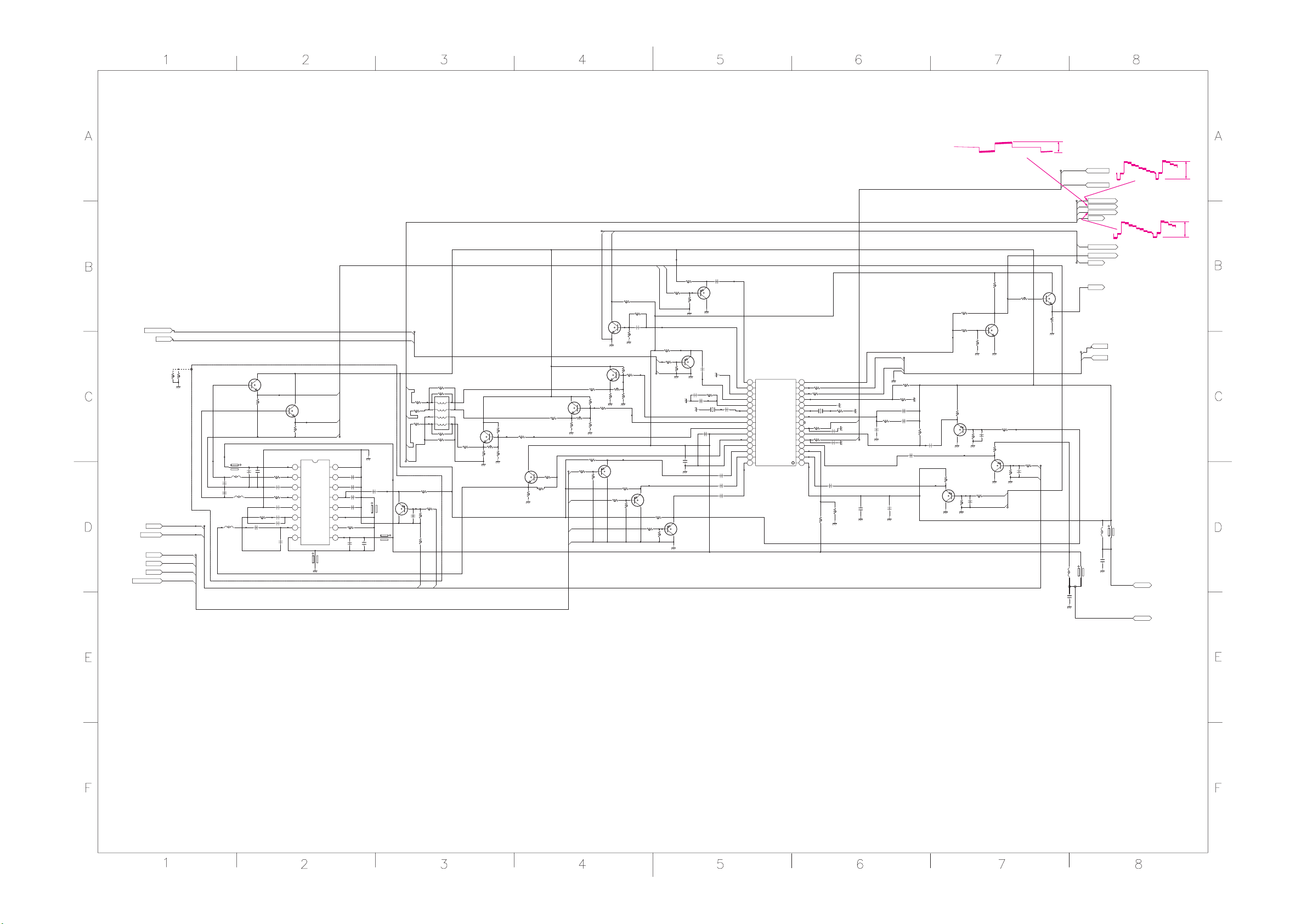
0.5Vp-p
C_AV_SUB
V_PIP
GND_PIP
SUB-Y
SUB-CB
SUB-CR
GND_SUB-Y
GND
GRZ01
KETSU
21
SUB-Y
SUB-CB
SUB-CR
KETSU
GRZ02
21
1
GND
V_PIP
GND_PIP
VD_HDMI
VD_HDMI
HD_HDMI
HD_HDMI
Y_CD_SUB
CB_CD_SUB
CR_CD_SUB
GND
TLC623
QY511
RY510
1.5k
CY512
+
TLC625
CY538
10V1000
QY504
2SA1576A
TLC627
CY504
B2200p
RY501
0.1uF
B25V0.01
CY506
30K
TLC629
XY501
CY502
CY501
B25V0.01
QY503
2SA1576A
CY526
0.1uF
CY525
0.1uF
CY524
0.1uF
TLC631
C1 IN
QY501
TA1340F
2.4
C1 IN
0.6
HD OUT
0
D GND
2.4
C2 IN
2.1
TLC630
CY505
APC FIL.
TLC632
4.1
X'TAL
3.5
12p
Cr OUT
3.4
Cb OUT
3.4
Y OUT
5.0
D-SYNC2 IN
5V
TLC633
3.0
FSC
0
GND2
1.9
Cr/R IN
2829 2627 2425 2223 2021 1819 161730
1.9
Cb/B IN Y1 IN
2.0
Y3/G IN 9V
TLC636
VD OUT
MONITOR
HD IN
VD IN
Y2 IN
SYNC OUT
GND1
HVCO
0.2
RY520
TLC638
100
3.5
SCL
TLC639
RY521
3.2
SDA
TLC645
100
2.8
ADD.
0
TLC648
TLC646
5.1
TLC640
6.2
AFC
0.1
2.0
0.1
2.3
TLC642
2.2
TLC643
2.3
2468 151412 1310 1197531
8.9
TLC644
XY502
TCR1023
RY592
100
RY591
RY585
RY561
470
HD_HDMI
CY591
KESTU
VD_HDMI
100
CY590
KETSU
CY513
0.1uF
CY539
10k
16V470
RY590
10k
CY518
+
CY508
0.1uF
OPEN
RY560
3.3k
SCL1
SDA1
RY503
CY516
B25V0.01
CY517
B16V1.0u
22k
RY581
KETSU
CY514
0.1uF
RY502
10k
TLC650
2SA1576A
OPEN
CY515
0.1uF
QY514
QY516
2SA1576A
TLC651
RY543
1.5k
RY573
4.7k
RY577
KETSU
OPEN
RY575
10k
TLC653
RY548
1k
RY547
TLC654
RY542
3.9K
TLC655
QY515
2SA1576A
RY541
6.8K
CY535
OPEN
RY576
12K
CY537
OPEN
1k
Y_COMB_S
QY518
RY545
100
RY552
1.5k
GND
2SC4081-Q
RY551
TLC658
1.8K
QY520
2SC4081-Q
RY562
100
R563
4.7k
TLC659
RY550
3.3k
V_PIP
GND
CY536
OPEN
LY012
10uH
CY541
10V470
HD_CD_SUB
RY507
1.0k
QY502
2SC4667
TLC614
TLC610
RY539
RY528
2.2k
RY531
RY533
2.7k
RY537
OPEN
TLC612
RY534
1k
JY509
RY540
OPEN
1k
2.7k
TLC616
1k
TLC613
QY513
2SA1576A
RY517
2.2k
RY525
2.2k
RY526
2.2k
LV272
RV357
RM73B1HR00OD
RV358
RM73B1HR00OD
RV359
RY110
1.5k
TLC607
2.2k
GND_PIP
GRV25
TLC580
TLC586
TLC585
GRV26
RY109
3.3k
RY107
GJ113
RM73B1HR00OD
GND_PIP
KETSU
GRV24
SHORT
GRV27
SHORT
V_PIP
SHORT
SHORT
QY507
2SC4081-Q
RY553
33
RY529
QY509
2SC4081-Q
RY555
33
RY536
OPEN
QY508
2SC4081-Q
RY554
JY508
RY530
RY532
100
TLC609
RY514
OPEN
RY515
RY519
OPEN
RM73B1HR00OD
33
1k
OPEN
RY518
2.2k
SUB-CR
RY527
2.2k
SUB-CB
SUB-Y
GND
RY535
OPEN
TLC608
JY507
KETSU
RY538
OPEN
1k
QY510
OPEN
1
BZ01
QY101
2SC4081-Q
TLC583
CY115
TLC582
TEM2120M
39p
33u
LY1 0 0
LY1 0 1
15u
LY1 0 4
LY1 0 5
PL-27
RM73B1H821JD
CY103
25V0.1
TLC584
TLC581
CY116
47p
TLC578
TLC579
CY109
RY103
1k
2SC4081-Q
+
RM73B1H221JD
RY105
CY112
100p
QY102
CY102
7L16V100u
CY106
B25V0.01
CY105
B25V0.01
TLC587
B25V0.01
180p
CY110
OPEN
TLC588
RY101
RY102
CY111
TLC597
RY104
1k
TC90A45F
4.9
TLC589
3.6
TLC590
1510 12119131416
1.6
3.8
TLC592
2.4
2.2
2.3
TLC594
0
Y_COMB_S
C_COMB_S
GND
QY100
Y_CD_SUB
GND
0
CY113
2.2
B25V0.01
CY114
2.8
B25V0.01
CY118
2.4
42375681
1.3
B25V0.01
TLC604
0
RY106
0
RM73B1HR00OD
TLC601
5.0
CY108
25V0.1
LY1 1 2
TEM2134AD
CY104
OPEN
CY107
7L16V10u
CY101
16V1u
+
CR_CD_SUB
CB_CD_SUB
TLC605
LY1 0 3
TEM2134AD
LY1 0 2
TEM2120M
TLC606
RM73B1HR00OD
QY103
2SA1576A
CY117
18p
RY504
CY582
100p
RY505
GND
RY508
2.2k
C_COMB_S
RY509
10k
4.7k
TLC619
12k
RY513
TLC624
1.5k
RY511
TLC620
C_AV_SUB
2.2k
RY512
2.2k
TLC617
B16V0.22_K
TLC618
QY512
2SA1576A
RY516
2.2k
RY523
TLC621
1.5k
RY524
2SA1576A
820
GND
HD_CD_SUB
VD_CD_SUB
GND
KVD
KVD
SDA1
SCL1
LY502
LY5 0 1
10uH
LY013
OPEN
+
OPEN
CY540
+
7L16V100u
9V
9V
1.7Vp-p
1.2Vp-p
5V2
26/32HL84
SIGNAL(V/C)
26HL84
SIGNAL (V/C)
SHEET-5/7
(5/57)

1-A1
R_VARIOUT
1-A1
L_VARIOUT
GND
GND
R_VARIOUT
L_VARIOUT
RS79
100K
RS80
100K
QS18
2SC3326B
RS116
RS112
QS17
2SC3326B
CS35
CS34
RS104
KETSU
RS28
1k
RS27
1k
CS39
10V1u
RS103
10k
MUTE_AUDIO
R_VARI
R_VARI
GND
GND
L_VARI
L_VARI
MUTE_AUDIO
7-B1
B16V1.0u
CS18
QS16
RN2404
KETSU
CS17
KETSU
B16V1.0u
47k
47k
R_HDMI-m
GND
L_HDMI-m
GND
R_HDMI-m
L_HDMI-m
RS83
KETSU
RS84
KETSU
QS20
KETSU
RS87
KETSU
RS88
KETSU
QS21
KETSU
QS19
KETSU
RS81
KETSU
RS82
KETSU
RS85
KETSU
RS86
KETSU
CS36
KETSU
CS37
KETSU
R_HDMI
L_HDMI
A_MUTE
GND
R_HDMI
GND
L_HDMI
A_MUTE
26/32HL84
SIGNAL(HDMI_VARI)
26HL84
SIGNAL (HDMI_VARI)
SHEET-6/7
(6/57)

MUTE_A
5V1
SPM
D615 D617
D613
MUTE_A
5V1
R630
4.7K
R631
22K
Q620
2SC2712Y
1SS355
D614
1SS355-TE17
1SS355-TE17 1SS355-TE17
R661
100K
C661
B1000p
R662
MUTE_AUDIO
C662
B1000p
MUTE_SPK
MUTE_AUDIO
MUTE_SPK
6-A2
5V1
ACDETECT
MUTE_E
5V1
ACDETECT
MUTE_E
R655
2.2k
D612
MA111
AC-OFF_Mute
C612
6.3V1000
Q612
2SA1162Y
+
R652
R650
1K
TLC0960
+
C653
7L50V1u
100K
+
C663R667
7L50V0.1
A_MUTE
D611
1SS355
A_MUTE
26HL84
SIGNAL (Audio-MUTE)
SHEET-7/7
(7/57)

2-D8
TV2V
GND
AOUT
GND
AFT2
V_TV
GND
GND
L_TV
R_TV
AFT1
GND
L_AV
R_AV
RESET_IMA
GND
R_VARI
L_VARI
5-A1
19P
PLUG B-B 19P
TV2V
GND
AOUT
GND
AFT2
V_TV
GND
GND
L_TV
R_TV
AFT1
GND
L_AV
R_AV
RESET_IMA
GND
R_VARI
L_VARI
MUTE_AUDIO
DET_FAULT
DET_HP
MUTE_SPK
GND
GND
GND
GND
GND
GND
5V2
5V2
5V2
32V
9V
9V
9V
3.3VA
3.3VA
12V
12V
SCL1
SDA1
19
TV2V
18
GND
17
AOUT
GND
16
15
AFT2
14
V_TV
13
GND
12
GND(0.75mm)
11
L_TV
10
R_TV
AFT1
9
GND(1mm)
8
L_AV
7
6
R_AV
RESET_IMA
5
4
NC
3
GND(1mm)
2
R_VARI
1
L_VARI
P103A
23P
PLUD B-B 23P
MUTE_AUDIO
1
DET_FAULT
2
DET_HP
3
MUTE_SPK
4
5
6
7
8
9
10
11
12
13
14
15
16
17
3.3VA
18
19
20
21
22
23
P104B
(TV-V_GND)
MUTE_AUDIO
DET_FAULT
DET_HP
MUTE_SPK
GND
GND
GND
GND
GND
GND
GND
GND
GND
GND
GND
GND
5V2
5V2
32V
32V
9V
9V
3.3VA
12V
12V
SCL1
SCL1
SDA1
SDA1
5-A1
(TV-GND)
4-C8
8-A1
SIGNAL
L-_AMP
L+_AMP
R-_AMP
R+_AMP
(NEJI-GND)
4-B2
L-_AMP
L+_AMP
R-_AMP
R+_AMP
12V_AUDIO
C691
GND
L_HP
R_HP
GND
B25V0.01
C692
B25V0.01
12V_AUDIO
GND
C693
B25V0.01
C694
L_HP
R_HP
GND
4P
P601
TLB0010
TLB0011
TLB0012
TLB0013
4P_2.5mm_1.5A_Beige
B25V0.01
8P
P809A
TLB0014
TLB0015
TLB0016
TLB0017
8P_2.5mm_1.5A_Beige
3P
P613A
3P_2.5mm_1.5A_Beige
1
L-_AMP
2
L+_AMP
R-_AMP
3
4
R+_AMP
1
12V(AUDIO)
2
12V(AUDIO)
3
12V(AUDIO)
4
12V(AUDIO)
5
GND(AUDIO)
6
GND(AUDIO)
GND(AUDIO)
7
8
GND(AUDIO)
L_HP(1mm)
1
R_HP(1mm)
2
GND(1mm)
3
SPK_R/L
(all:2mm)
POWER
FRONT-AV
26HL84
TN-AOUT (CONNECTOR)
SHEET-1/8
(8/57)

0
3.5
4.1
3.2
5.0
32.1
9.1
3.202.4
4.1
2.9
5.0
4.0
3.2
3.5
5.0
0
32.0
0
4.0
0
2.6
9.1
0.2
5.205.2
3.8
3.6
5.2
3.7
3.3
3.603.5
3.2
2.002.0
2.0
8.8
26HL84
TN-AOUT (TIF & MA)
SHEET-2/8
(9/57)

R_APRO
L_APRO
GND
IMA MODULE TERMINAL (#25pin GND)
12V
GRS01
OPEN
R_APRO
L_APRO
GND
DS102
MA8056-M
RS515
3.9K
12V
CS510
B16V1u_K
CS501
7L50V10u
RS516
47K
RS517
47K
++
CS503
7L50V10u
GRS02
OPEN
RS501
10K
0
3412
5.2
5.6
5.5
5.6
5.6
6578
RS505
RS504
39k
10K
All pants should be laid close by IMA Module.
RS500
39k
CS505
OPEN
5.6
12.0
CS504
OPEN
QS102
BA10358F-E2
CS502
B16V2.2u_K
RS506
4.7K
RS507
4.7K
R_VARI
L_VARI
5-A1
R_VARI
GND
L_VARI
GND
26HL84
TN-AOUT (IMA MOPULE)
SHEET-3/8
(10/57)

The surface patterns under Q610 should be GND, and make many more through-holes between surface GNDs as much as possible.
1-C5
(Audio±GND)
(4mm)(Audio±Vcc)
(4mm)
5-A1
MUTE±AUDIO
Chassis GND for screws
1-D3
TLC0938
1
12V±AUDIO
TLC0939
1
GND
(GAISHUU±GND)
5-A1
R±VARI
L±VARI
GND
GR607
KETSU
GR608
KETSU
11
9V
MUTE±SPK
TLC0956
DET±HP
12V±AUDIO
21
21
9V
MUTE_SPK
1
2
C602
B330p
1
1
R_VARI
L_VARI
L643
KETSU
21
L645
TEM2142AD
12
DET±HP
Corresponded to shielding (should be enclosed with GND)
GND
1
D620
R616
1SS355
TLC0991
1
C615
+
2
7L16V100u
1
D646
1SS355
2
Q677
RN2404
1
2
R615
100K
D629
R614
3
TLC0962
10k
1SS355
TLC0975
1
1
1
21
21
1
1
R619
TLC0992
47K
21
Q678
2SC2712Y
2
TLC0994
3.3K
1
21
1
1
1
2
21
R618
22K
TLC0993
1
3
3
2
B
CE
CE
2
B
1
1
Q679
1
1
2SC2712Y
C687
R680
50V1500p
47k
2
1
21
1
TLC1000
C665
R672
7L50V10u
R_VARI
GND
L_VARI
GND
4.7k
21
2
1
C666
7L50V10u
++
2
1
1
TLC1001
3
C
R677
TLC0997
2
47K
21
R673
1
1k
B
1
E
Q672
2SC3326B
C688
R681
50V1500p
47k
2
1
21
MM
R670
TLC0995
4.7k
21
1
3
21
Q671
2SC3326B
21 21
C
2
R671
1k
B
1
E
R676
47K
Q680_C
B16V1.0u
2
C678
B390p
1
B16V1.0u
2
C677
B390p
1
AUDIO OUTPUT (R/L )
L625
TLN3528AF
12V±AUDIO
L655
TEM2137AD
12
TA2024
5.0
+5VGEN
TLC1006
15.8
1 1
C601
2
DCAP2
TLC1007
0.1uF
6.5
C610
TLC1004
2
1
1
C613
2
1
R646
10k
Q680
2SC2712Y
1
1
DCAP1
TLC1008
5.0
C603
1
2
0.1uF
1
R604
8.2K(1%)
C604
B2.2u
2
C608
0.1uF
1
21
R609
27K
21
2
C611
R611
0.1uF
1K
1
21
R612
27K
2
C614
0.1uF
1
2
21
B
1
TLC1009
21
1
2
1
TLC1010
R610
21
1
TLC1011
120K
1
TLC1012
1
TLC1013
R613
21
1
TLC1014
120K
1
TLC1015
1
1
(A-GND)
21
R645
10k
1
3
CE
1SS355
1
V5D
0
AGND1
0.1
REF
1.8
OVERLOADB
0
AGND2
5.0
V5A
2.4
VP1
2.4
IN1
0
MUTE
NC
2.4
VP2
14 13 12 11 10 9 8 7 6 5 4 3 2 1
2.4
IN2
2.0
BIASCAP
0
AGND3
0
SLEEP
18 17 16 15
1
2
D642
Q610
L640
1uH
21
MA8062-L
CPUMP
PGND1
3533 34 3630 3128 292524 262119 20 22 23 27 32
NC
VDDA
NC
OUTP1
VDD1
VDD1
OUTM1
OUTM2
VDD2
VDD2
OUTP2
NC
DGND
NC
PGND2
FAULT
21
1
(D-GND)
C630
0.1uF
2
1
D657
21.4
TLC1031
1
0
TLC1032
13.1
6.4
13.1
TLC1033
13.1
1
6.5
6.5
13.1
13.1
6.5
0
0
0
TLC1043
1
21
R642
1K
1
2
C629
7L50V1u
+
2
1
C627
0.1uF
2
1
C635
16V220
2
1
C624
2
1
0.1uF
C621
2
1
0.1uF
C636
++
2
1
16V220
21
D656
MA8150-M
1
D643
1SS355
TLC1045
1
TLC1048
TLC1049
TLC1050
TLC1046
TLC1047
1
1
1
1
1
1SS355-TE17
1SS355-TE17
D624
D625
1SS355-TE17
1
4
41
1
D621
2
1SS355-TE17
1
D622
2
1SS355-TE17
D623
1
2
1SS355-TE17
1
2
1
2
D626
1SS355-TE17
1
2
1
D627
2
1SS355-TE17
1
2
D628
L620 L622
TLN3528AF TLN3528AF
1
4
41
DET±FAULT
L623
TLN3528AF
23
1
2
3
4
41
2
C625
0.22uF
1
2
C623
B16V0.22_K
1
C622
B16V0.22_K
1
2
C620
B16V0.22_K
1
23
1
2
3
4
41
23
2
3
2
C646
0.47u
1
TLC1052
1
R623
1/8W10
21
212
C647
0.47u
TLC1053
1
R620
1/8W10
21
23
2
3
TLC1056
1
TLC1058
1
TLC1059
1
R+±AMP
2
C648
0.1u
1
R-±AMP
L-±AMP
2
C649
0.1u
1
L+±AMP
R+±AMP
R-±AMP
L-±AMP
L+±AMP
DET±FAULT
(1.25mm)
(1.25mm)
(1.25mm)
(1.25mm)
1-D3
26HL84
TN-AOUT (A-OUT)
SHEET-4/8
(11/57)

9V
TLC1064
(P611A#3-GND/1.5mm)
GND
4-B2
MUTE_AUDIO
R_VARI
L_VARI
R_VARI
L_VARI
HP-AMP
9V
Q630
LA4525
0
1.4
R687
47K
MUTE_AUDIO
R696
KETSU
2SC3326B
C632
B0.22u
Q675
C672
B16V2.2u_K
R679
2.2K
TLC1070
C679
TLC1069
220p
R686
47K
C667
10V1u
R660
56K
R695
KETSU
R678
2.2K
C631
B0.22u
C668
10V1u
220p
C669
TLC1071
1.4
5678
C673
B16V2.2u_K
56K
R674
Q676
2SC3326B
R601
2R47
C644
KETSU
D608
MA8100-M
TLC1075
3.5
8.0
3.4
TLC1076
M
C645
B0.01
+
C640
10V1000
TLC1077
D640
1SS355
TLC1079
3412
D672
0
1SS355
1SS355
D673
R664
KETSU
++
C641
7L16V47u
R663
KETSU
C642
7L16V47u
TLC1082
C643
KETSU
D641
1SS355
R640
10k
R641
10k
R_HP
L_HP
GND
R_HP
L_HP
(HP-GND/1mm)
26HL84
TN-AOUT (HP-AMP)
SHEET-5/8
(12/57)

RT01
10K
PT01
CONNECTOR
3
2 NC
1
26HL84
TN-AOUT (TEMP-SENSOR)
SHEET-6/8
(13/57)

8-B2
8-B2
BD01
9V
9V
3.3VA
3.3VA
GND
(Analog-GND) (Digital-GND)
L_AD-IN
R_AD-IN
R_DA-OUT
R_DA-OUT
L_DA-OUT
L_DA-OUT
TEM2121M
CD121
25V0.1
CD123
25V0.1
LD102
LD103
TEM2121M
CD122
25V0.1
CD124
25V0.1
CD210
DD209
MA111
RD249
100
DD210
MA111
RD250
100
(Analog-GND)
+
CD209
10V47
B10V4.7u
CD203
B10V4.7u
B6.3V10u_K
CD201
25V0.1
CD202
CD204
B470p
CD205
CD206
CD207
25V0.1
B470p
25V0.1
+
CD211
QD205
TA78L05F
IN OUT
321
CD212
25V0.1
5V
CD213
+
10V4716V47
LD201
QD202
PCM3001E
2.1
RSTB
V L
IN
5.1
FMT0
V 1
CC
0
364510 8913 1214 11 7 12
FMT1
AGND1
2.1
FMT2
V L
REF
2.1
DGND
V R
REF
2.1
V R
V
IN
DD
2.1
C PR
CLKIO
IN
2.1
C NR
XTO
IN
2.1
C NL
XTI
IN
2.1
DOUT
C PL
IN
2.5
DIN
VCOM
2.5
V R
BCKIN
OUT
0
AGND2
LRCIN
5.1
V 2
V L
CC
OUT
CD234
B16V0.47_K
RESET1
3.3k
RD236
100
RD212
100
RD240
100
RD237
RD238
100
100
LD203
TEM2121M
B6.3V10u_K
RESET2
PD1
CD233
CD230
3.6
3.6
3.6
3.6
3.6
3.6
25 26232117 1815 16 2019 22 24 27 28
QD207
TMP87C409M
1.9
TLC74
XOUT
1.1
TLC76
0
364510 8913 1214 11 7 12
0
XIN
TCR1082AM
XD02
QD208
PST9129NR
1
NC
2
SUB
GVou
3
MA111
DD205
TEM2121M
RSTB
JP
QD203
RSTB
RD210
0.3
100
RD233
CD208
25V0.1
RD206
100
RD201
100
RD209
KETSU
RD208
4.7k
RD207
KETSU
RD230
1k
RD232
KETSU
1k
RD205
10k
RD204
100
RD203
100
RD239
100
0.1
5.0
26232117 1815 16 2019 22 24 27 28
0.1
25
0
5.1
1.7
0.1
1.6
1.2
1.8
1.8
2.5
TC7SH32FU
0
1
1.6
2
0
3
RD220
100
RD222
10k
RD224
10k
RD225
100
RD226
100
0
1OE
1.3
1A
1.8
1Y
3645712
0
2OE
1.3
2A
1.8
2Y
0
GND
2.5
54
CD222
25V0.1
0.8
0.8
RD221
10k
RD223
10k
1.2
0.3
1.3
RD229
2.6
VCC
0
4OE
1.2
4A
12 1413108 9 11
1.7
4Y
0
3OE
0.8
3A
1.0
3Y
25
0
SDI1
26
0
27
TEST3
0
LRI
28
0
BCKI
29
MCK
30
BCKO
31
LRO
32
100
CD221
25V0.1
2.5
0
0
VDDR
VSSR
VSSR
SDIO
QD201
NJU26103
TEST0
TEST1
SDO0
9.8
RD211
100
CD223
25V0.1
2.500
4213 8567
0
RD202
QD204
TC74VCX125FT
VDDR
SEL1
3.6
10k
VSSC
SCL/SCK
RD213
SCL
CD224
25V0.1
100
CD220
25V0.1
2.5
2.5
19 18 1724 22 2123 20
16
VSSC
VDDC
VDDC
0
TEST2
VSSC
15
CD219
2.5
25V0.1
VDDC
14
3.6
RESETX
13
RD219
0
12
11
10
25V0.1
9
CD226
1.2
1.1
2.5
100
CD215
25V0.1
CD214
QD206
PQ025EZ5MZP
Vin21
On/Off 4
GND
5
4.7K
RD227
+
10V47
TEM2121M
Vo
NC
RD228
4.7K
LD204
3
CD227
25V0.1
VSSO
XO
XI
VDDO
AD2/
SSX
AD1/SDIN
SDA/SDOUT
3.602.5
10k
10k
100
RD216
RD215
RD214
SDA
++
CD225
10V47
RD218
240
RD217
1M
2.5V
XD01
AT-51(24.576)
CD228
10V47
CD216
B1000p
CD218
10p
CD217
27p
LD202
CHIP-INDUCTOR-2R2MMHJ
(Digital-GND)
LD205
RD251
SDA
SCL
DD206
MA111
3.3k
RD243
KETSU
DD204
MA111
VCC
DD203
CD235
25V0.1
MA111
DD202
MA111
5
4
DD201
MA111
RD248
RD235
CD231
open
47K
3.3k
RD234
CD232
open
The outsides of shield plate should be Analog GND.
26HL84
TN-AOUT (LipSync DIGITAL PART)
SHEET-7/8
(14/57)

9V
9V
RD130
1.8K
L_LS-OUT
GND
R_AV
L_AV
GRD01
GRD02
L_LS-OUT
GND
KETSU
KETSU
L_AV
R_AV
CD120
B16V1u_K
DD101
MA8039-L
RD115
2.2K
CD114
B16V2.2u_K
CD101
RD101
82k
B10V4.7u
CD102
RD102
47K
QD101
BA10358F-E2
RD107
RD106 RD108
CD104
82k
B10V4.7u
CD105
RD114
47K
CD113
100p
270p
47K
270p
RD113
CD118
B10V4.7u
LD101
TEM2121M
R_AD-IN
GND_D
R_AD-IN
GND_D
0
RD103
33K
RD104
39K
3412
3.6
3.6
CD103
100p
RD105
4.7k
3.6
(Analog-GND) (Digital-GND)
3.6
3.6
3.6
9.1
6578
CD119
B10V4.7u
CD106
100p
33K
RD109
CD112
560p
RD111
15k
22K
39K
CD111
B10V4.7u
CD107
B16V2.2u_K
RD110
4.7k
L_DA-OUT
L_AD-IN
L_AD-IN
L_DA-OUT
GND
R_LS-OUT
GND
R_LS-OUT
QD102
BA10358F-E2
RD120
2.2K
RD112
CD116
560p
47K
RD116
22K
RD117
47K
CD115
B10V4.7u
R_DA-OUT
R_DA-OUT
6578
9.1
3.6
3.6
3.5
0
3412
3.6
3.6
3.6
CD117
RD118
100p
15k
RD119
47K
26HL84
TN-AOUT (LipSync ANALOG PART)
SHEET-8/8
(15/57)

KEY
SA07 SA01SA02SA03SA04SA06
MENU
VIDEO
RA76 RA75
PA 05 B
15k
5V1
8.2k
356412
NC
KEY-1
KEY-2
MICRO GND
RA71 RA73RA72
27k 8.2k15k
PLUG 6P
MAIN GND
SA05
POWERVOL UPVOL DN POS UPPOS DN
26/32HL84
KEY
26HL84
CONT (KEY)
SHEET-1/2
(16/57)

POW-SW
S801
SWITCH PUSH 2C2P
6
1
KEY-1
NC12GND
3
34
TLB0006 TLB0005
PJ60A
3P±2.5mm±1.5A
26/32HL84
POWER SW
26HL84
CONT (POWER SW)
SHEET-2/2
(17/57)

SCALER
5V-1
PLUG 5P
RESET
PLUG 5P
GND-D
RESET
CNVSS
SCLK
BUSY
3.3V-3
55
SDA
44
33
22
GND
11
SCL
PJ91A
5
SDA
4
3 VCC3
VCC
SCK
PJ93A
11FMN-SMT-A-TF
PJ94A
1
NC
3
4
TXD
5
RXD
6
EPM
SDA
RESETRESET
5V-1
GND
SCL
PJ91B
5P_2.5mm_1.5A_Black
5
SDA
4
RESET
2 GND2GND
1 SCK1
PJ93B
5P_2.5mm_1.5A_Beige
11
NC
10 GND-D2
9 RESET
8 CNVSS
7 TXD
6 RXD
5 SCLK7
4 BUSY8
3 EPM9
2CE10CE
1 3.3V-311
PJ94B
JIGU
11FMN-BTK-A
26/32HL84
DATA_REWRITE
26HL84
DATA_REWRITE
(18/57)

E3
R
L
S VHS 1P JACK
S
V
L
R
PIN JACK 3P
JACK 2P
PV61
PV60
PS02
R
M
L
GSR06
SHORT
GSR05
SHORT
GR605
RC16
SHORT
RC15
GR604 CC09
KETSU B1000p
RC12
680
RC11
680
B1000p
GSR11
KETSU
CC15
CC14
B1000p
PV23A
R_HDMI-m
123456789
L_HDMI-m
GND
19FMN-BTK-A
DET_HP
GSR10
KETSU
GND
R_DVI
L_DVI
GND
RV122
1/8W75
GRV16
CV121
OPEN
0.01
RV121
1/8W75
RV129
100
RV120
CC10
B1000p
1/8W75
DV120
KETSU
23118529/23316672
DET_HP
680
680
GND
GND
L_E
R_E3
GND
C_E3
YV_E3
3
Y_E3
GND
1011
C_E3
S-SW_E3
1213141516171819
GND
V_E3
GND(Audio)
L_E3
R_E3
TUNER GND(2mm)
TUNER GND(2mm)
SIGNAL
P661
EARPHONE J D3.5
R690
1/8W150
R688
1/8W150
C606
B1000p
C605
B1000p
M
CY650
50V1000p
D653
KETSU
D652
KETSU
R_HP
L_HP
HP_GND
312
R_HP
L_HP
P613B
3P_2.5mm_1.5A_Beige
TN-AOUT
26/32HL84
FRONT-AV(AV-1)
26HL84
FRONT-AV (AV-1)
SHEET-1/2
(19/57)

OUT
VARIABLE
MONITOR OUT
(MAIN/SUB)
L
R
V
L
R
PV05
JACK 5P
M2
L2
R1
M1
L1
LC03
TEM2121M
LC04
TEM2121M
LC02
TEM2121M
LC01
TEM2121M
CC12
1000p
L_VARIOUT
R_VARIOUT
CC18CC19
1000p1000p
V_MONI
L_MONI
R_MONI
RS31
100k
RS32CC11
100k1000p
PV22B
1
L_VARIOUT
2 R_VARIOUT
GND
3
4
GND
5
L_MONI
6
R_MONI
7
GND
8
GND_V_MONI
9
V_MONI
PLUG B-B 9P
SIGNAL
\U+2550ÅP\U+2550\U+00D9\U+2550\U+00D0
\U+2550ÅP\U+2550\U+00D9\U+2550\U+00D0
26/32HL84
FRONT-AV(AV-2)
26HL84
FRONT-AV (AV-2)
SHEET-2/2
(20/57)
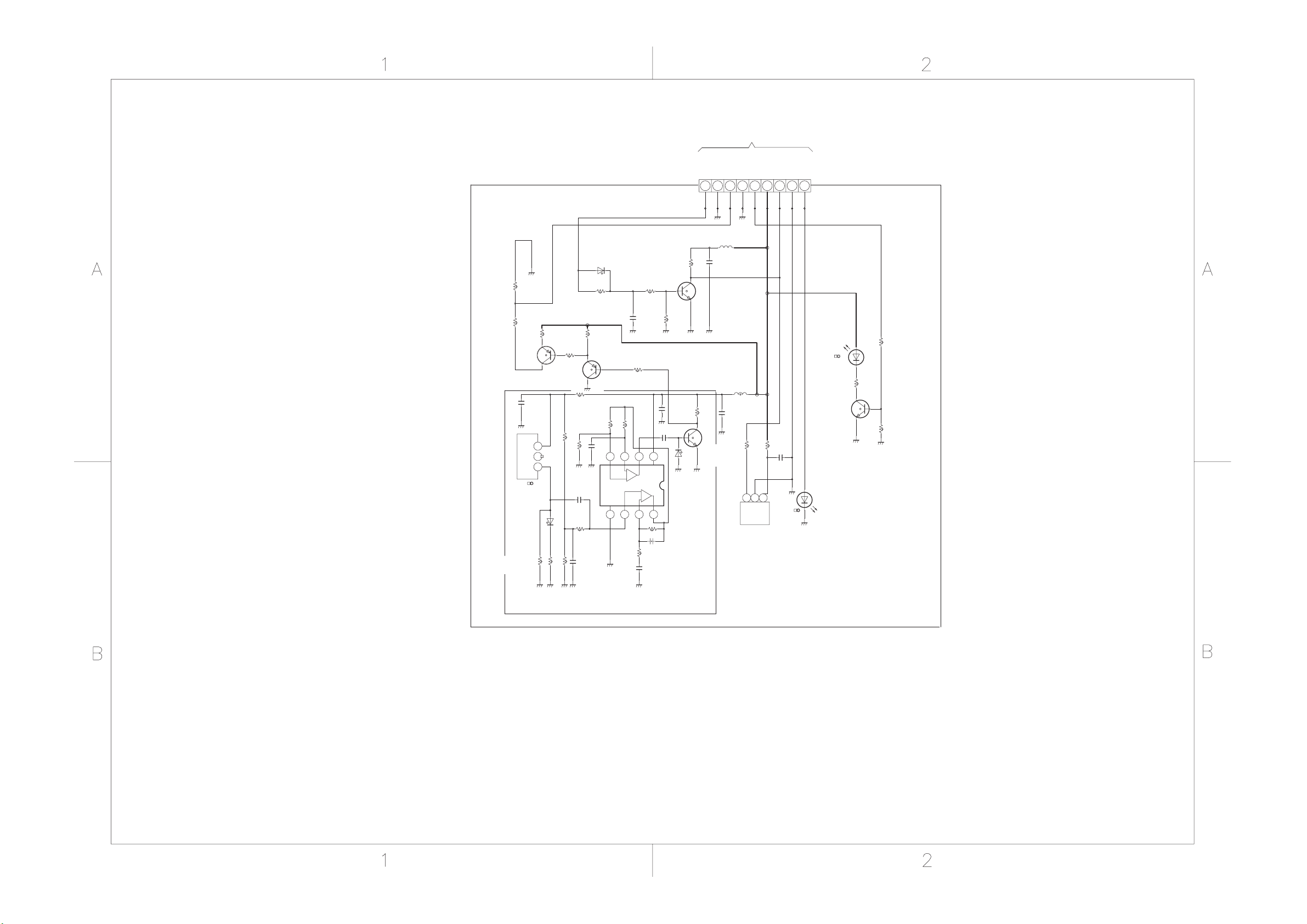
RB71
1.0
22 56
RB72 RB73
QB54
2SA1576A
+
CB60
16V10
RPM-676CBR-S
3
2
DB51
1
HPI-2FPR4
HOLDER, RMT
DB51A
HOLDER(C025045E)
DB52
1SS355-TE17
1SS355-TE17
RB51
220k
1SS355-TE17
RB69
2.7k
RB70
330
RB63
270
12k
RB53
RB60
220k
CB51
50V0.010u
M
RB55
220k
CB52
+
16V47
1SS355-TE17
DB53
RB64
1k
QB53
2SA1576A
RB59
CB55
50V1.0
+
5876
1.2k
M
RB67
220
10k
RB58
+
243 1
M
RB66
RB65
220
CB57
63V0.10
M
CB59
50V0.010u
M
+-
RB57
10k
CB54
RB56
150
CB53
63V0.10
47k
QB55
2SC2712Y
100k
RB74
RB62
2.7k
CB61
63V0.10
1SS355-TE17
QB52
2SC2712Y
DB54
1SS355-TE17
QB51
M5218AP
B220p
TO SIGNAL
PB22A
GND
IN
OUT
GND
LED
5V1
89215476 3
RB15
GND
VOUT
KB01
TLA071 TLA072TLA1
470
16V47
321
Vcc
TLA075TLA076 TLA067TLA2 TLA074TLA073
LB52
100MH
+
CB58
16V47
LB51
0.10
+
CB56
16V47
PIC-37043TE2
GND
REM OUT
REM IN
PLUG 9P
PB22B
PLUG 9P
DB01
DB01A
LED HOLDER C025276E
RB01
QB01
47
RB19
+
2SC2712Y
CB01
DB03
SIR-56SB3F
DB03A
LED HOLDER C025276E
RB05
SLR_56VC3FPQ
1k
SLR-56VC3FPQ
390
RB04
47k
2SC2712, Y
IR-PASS/RMT/LED
RB52
12k
RB54
12k
SHIELD
26/32HL84
IR-PASS/RMT/LED
26HL84
IR-PASS/RMT/LED
(21/57)
 Loading...