Toshiba 26HL83, 26LH83 Schematic

FILE NO. 010-200311
DOCUMENT CREATED IN JAPAN, Sep., 2003
SERVICE MANUAL
LCD TELEVISION
26HL83

TABLE OF CONTENTS
SERVICE SAFETY PRECAUTIONS .................................................................................................................................... 3
HANDLING THE LCD MODULE .......................................................................................................................................... 5
LOCATION OF CONTROLS ................................................................................................................................................ 7
LAYOUT OF MAJOR BOARDS ............................................................................................................................................ 9
MECHANICAL DISASSEMBLY.......................................................................................................................................... 10
PACKING DISASSEMBLY .................................................................................................................................................. 26
GENERAL ADJUSTMENTS
WIRING CONNECTION DIAGRAM ................................................................................................................................... 27
CHASSIS AND CABINET REPLACEMENT PARTS LIST ................................................................................................. 31
PC BOARDS BOTTOM VIEW ............................................................................................................................................ 41
CIRCUIT BLOCK DIAGRAM..............................................................................................................................................48
SPECIFICATIONS.......................................................................................................................................................... END
APPENDIX:
CIRCUIT DIAGRAM
SPECIFIC INFORMATIONS
– 2 –

SERVICE SAFETY PRECAUTIONS
• The caution items shown here describe major safety issues and should always be observed.
• The meanings of the various indications are as follows.
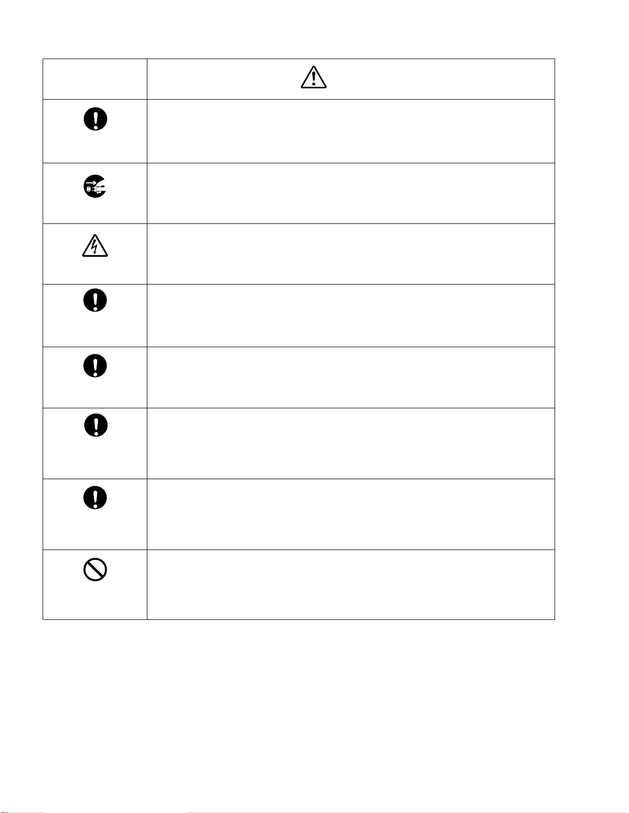
WARNING
CAUTION
* Physical damage means major damage to a home, furnishings and other possessions.
Examples of marks
SHOCK HAZARD
PROHIBIT DISASSEM-
BLING
UNPLUG
Indicates a hypothetical situation in which service personnel and nearby third parties, or even
end users due to a product defect after the service operation is completed, could possibly be in
danger of injury or even death in the event of operational error.
Indicates a hypothetical situation in which service personnel and nearby third parties, or even
end users after the service operation is completed, could possibly be in danger of injury, or
where there could be physical damage in the event of operational error.
The > indicates caution (including danger and warning).
The actual meaning of this caution is indicated inside the > or nearby illustrations or text.
The example shown to the left indicates the danger of "electrical shock".
indicates a forbidden action.
The
The actual meaning of this caution is indicated inside the or nearby illustrations or text.
The example shown to the left indicates that disassembly is forbidden.
The a indicates a forced action (an action that must be performed).
The actual meaning of this forced action is indicated by a or nearby illustrations or text.
The example shown to the left indicates that the power plug must be disconnected.
GENERAL ADJUSTMENTS
SPECIFIC INFORMATIONS
– 3 –
KEEP CHILDREN
AWAY
GENERAL ADJUSTMENTS
UNPLUG
SHOCK HAZARD
USE SPECIFIED
PARTS
SPECIFIC INFORMATIONS
CAUTION FOR
WIRING
CAUTION FOR
ASSEMBLING /
WIRING
WARNING
• Always advise users to keep children away.
There is danger of injury to children from tools, disassembled products, etc.
• Always disconnect the power plug before starting work whenever power is not required.
Failure to disconnect the power plug before starting work can result in electrical shock.
• Depending on the model, use an insulation transformer or wear gloves when servicing with the
power on, and disconnect the power plug to avoid electrical shock when replacing parts.
In some cases, alternating current is also impressed in the chassis, so electrical shock is possible if the chassis is contacted with the power on.
• Always use the replacement parts specified for the particular model when making repairs.
The parts used in products have the necessary safety characteristics such as inflammability,
voltage resistance, etc.; therefore, use only replacement parts that have these same characteristics.
Use only the specified parts when the * mark is included in a circuit diagram or parts list.
• Parts mounting and routing of the wiring should be the same as that used originally.
For safety purposes, insulating materials such as tubing or tape is sometimes used and printed
circuit boards are sometimes mounted floating.
Also make sure that wiring is routed and clamped to avoid parts that generate heat and which
use high voltage. Always follow the original scheme.
• After a repair has been completed, reassemble all disassembled parts, and route and reconnect the wiring, in accordance with the original scheme.
Do not allow internal wiring to be pinched by cabinets, panels, etc.
Any error in reassembly or wiring can result in electrical leakage, flame, etc., and may be
hazardous.
CHECK INSULATION
RESISTANCE
PROHIBIT
REMODELING
• After completing the work, disconnect the power plug from the outlet, remove the antenna, turn
on the power switch. Then, use a 500V insulation resistance meter to check the insulation
resistance of the antenna terminal, other metallic parts and between the prongs of the power
plug to make sure that the insulation resistance is 1M Ω or more.
The set will require inspection and repair if the insulation resistance is below this value.
• Never remodel the product in any way.
Remodeling can result in improper operation, malfunction, or electrical leakage and flame,
which may be hazardous
– 4 –

HANDLING THE LCD MODULE
Safety Precautions
In the event that the screen is damaged or the liquid crystal
(fluid) leaks, do not breathe in or drink this fluid. Also, never
touch this fluid.
Such actions could cause toxicity or skin irritation. If this fluid
should enter the mouth, rinse the mouth thoroughly with water. If the fluid should contact the skin or clothing, wipe off
with alcohol, etc., and rinse thoroughly with water. If the fluid
should enter the eyes, immediately rinse the eyes thoroughly
with running water.
Precautions for Handling the LCD Module
The LCD module can easily be damaged during disassembly
or reassembly; therefore, always observe the following precautions when handling the module.
1. When attaching the LCD module to the LCD cover, position it appropriately and fasten at the position where the
display can be viewed most conveniently.
3. If the panel surface becomes soiled, wipe with cotton or a
soft cloth. If this does not remove the soiling, breathe on
the surface and then wipe again.
If the panel surface is extremely soiled, use a CRT cleaner
as a cleaner. Wipe off the panel surface by drop the cleaner
on the cloth. Do not drop the cleaner on the panel. Pay
attention not to scratch the panel surface.
GENERAL ADJUSTMENTS
4. Leaving water or other fluids on the panel screen for an
extended period of time can result in discoloration or
stripes. Immediately remove any type of fluid from the
screen.
SPECIFIC INFORMATIONS
2. Carefully align the holes at all four corners of the LCD
module with the corresponding holes in the LCD cover
and fasten with screws. Do not strongly push on the module because any impact can adversely affect the performance. Also use caution when handling the polarized screen
because it can easily be damaged.
The metal edges of the LCD module
CAUTION
are sharp, so use caution to avoid injury.
5. Glass is used in the panel, so do not drop or strike with
hard objects. Such actions can damage the panel.
6. CMOS-LSI circuitry is used in the LCD module, so avoid
damage due to static electricity. When handling the module, use a wrist ground or anchor ground.
– 5 –
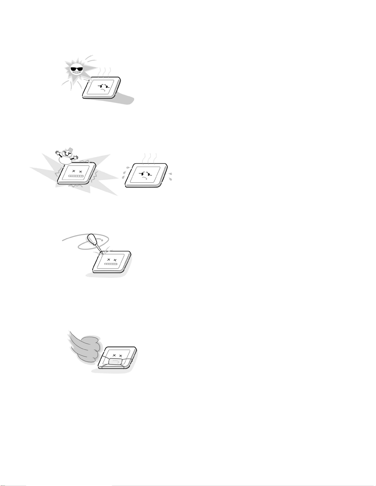
7. Do not expose the LCD module to direct sunlight or strong
ultraviolet rays for an extended period of time.
GENERAL ADJUSTMENTS
SPECIFIC INFORMATIONS
8. Do not store the LCD module below the temperature conditions described in the specifications. Failure to do so
could result in freezing of the liquid crystal due to cold air
or loss of resilience or other damage.
9. Do not disassemble the LCD module. Such actions could
result in improper operation.
10. When transporting the LCD module, do not use packing
containing epoxy resin (amine) or silicon resin (alcohol or
oxime). The gas generated by these materials can cause
loss of polarity.
– 6 –
Remote sensor
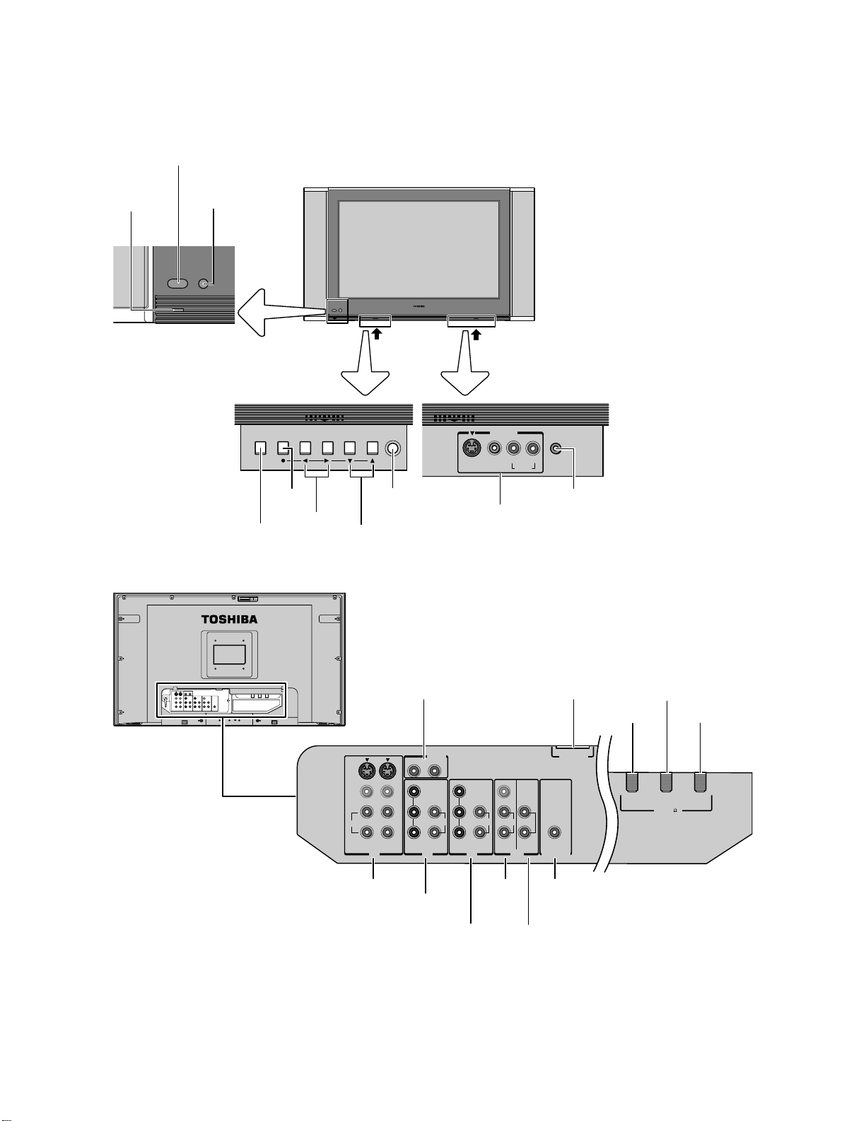
LOCATION OF CONTROLS
Power
indicator
TheaterLink
(IR pass through)
POMER
Left pocket panel Right pocket panel
TV/VIDEO
Back
TV front
POMER
Push up Push up
TV/VIDEO MENU VOLUME CHANNEL POWER
MENU
Volume T S
Menu T S
POWER
Channel ts
Menu ts
VIDEO-3 IN
S-VIDEO VIDEO RL/MONO
VIDEO-3
INPUT
AUDIO
HEADPHONE
Headphones
jack
GENERAL ADJUSTMENTS
SPECIFIC INFORMATIONS
DVI/HDCP
AUDIO IN
COLOR
STREAM
HD-1
R
Y
P
P
DVI/HDCP
AUDIO IN
B
R
L
L
AUDIO
S-VIDEO
VIDEO
L /
MONO
AUDIO
RR
VIDEO 1 VIDEO 2
IN IN IN OUT
VIDEO 1/2
ColorStream
HD-1
ColorStream
HD-2
– 7 –
VIDEO
Y
L /
P
B
LL
AUDIO AUDIO
P
R
RRR
COLOR
STREAM
HD-2
VIDEO/
AUDIO OUT
DVI/HDCP
VAR
AUDIO
MONO
TheaterLink OUT
TheaterLink
OUT
Variable
AUDIO OUT
DVI/HDCO IN
ANT OUT
ANT-1 IN
ANT 1
OUT
ANT( 75
ANT-2 IN
ANT 2
)
Remote Control
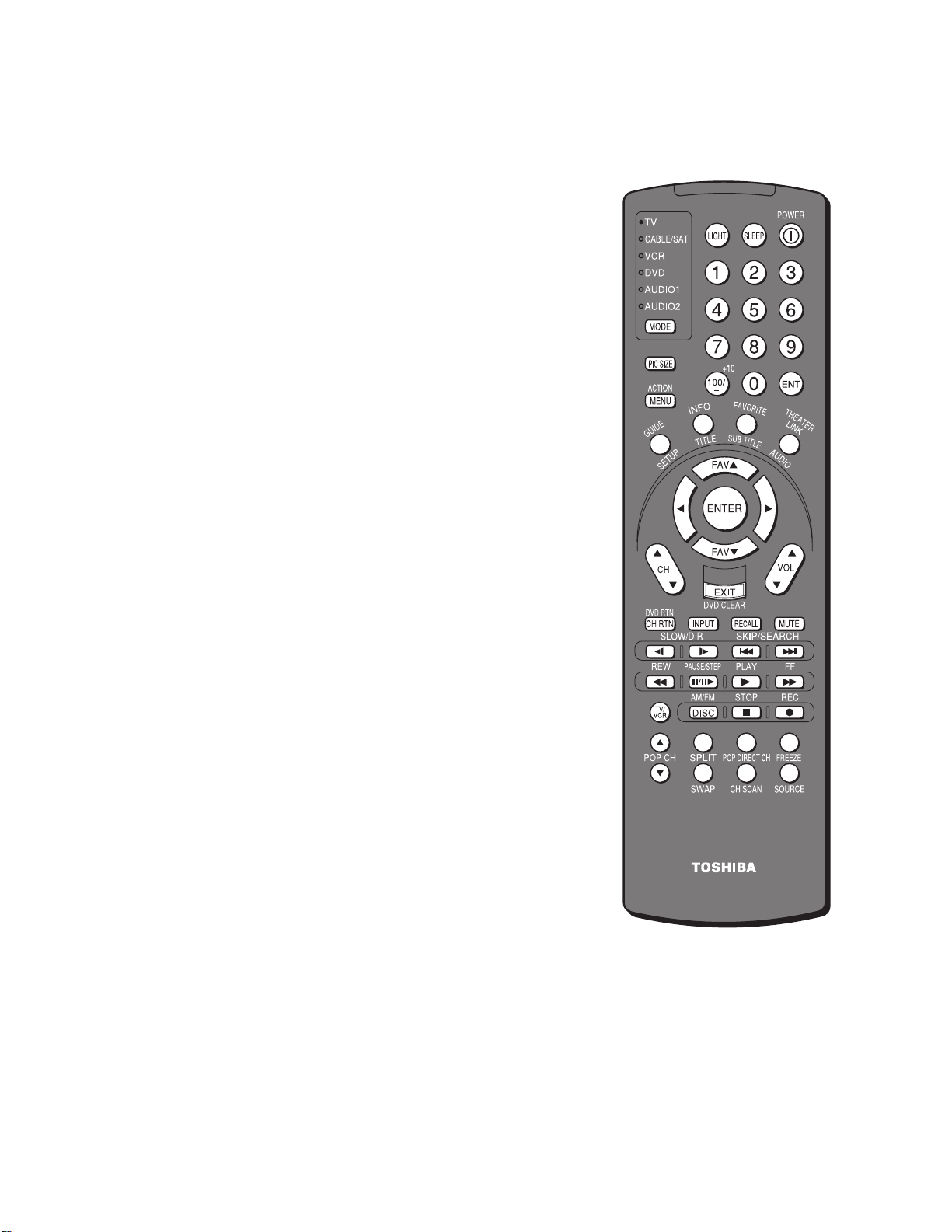
POWER turns the TV on and off.
SLEEP allows access to the automatic TV shut-off function .
LIGHT The first press of the LIGHT button lights the keypad and turns on
the Illumination mode. With the Illumination mode on, pressing any
other key lights the keypad for 5 seconds (10 seconds if you’re in
programming mode).
Subsequent presses of the LIGHT button toggle between turning
the Illumination mode on and off.
GENERAL ADJUSTMENTS
Channel Numbers (0-9, 100) allow direct access to channels.
MODE cycles through the six device modes: TV, CABLE/SAT, VCR, DVD,
AUDIO1, and AUDIO2. The mode indicator light will remain lit for a
few seconds.
PIC SIZE cycles through the five pictures sizes: Natural, Theater Wide 1,
2, 3, and Full.
FAVORITE allows access to the favorite channel search function
.
MENU allows access to on-screen programming menus.
SPECIFIC INFORMATIONS
ENTER sets programming menu information.
st T S select or adjust programming menus.
FAV st cycles through favorite channels.
CH st cycles through programmed channels.
VOL st adjusts the volume level.
EXIT exits the programming menus.
INPUT selects the video input source.
MUTE mutes the sound.
RECALL displays on-screen information.
CH RTN returns to the last viewed channels.
POP CH st selects the POP (picture-out-picture) channel.
SPLIT turns the POP feature on and off.
CH SCAN allows access to the programmed channel search function
.
FREEZE freezes the POP picture.
SWAP switches the main and POP pictures.
Note:
The error message "Not Available" will appear
if you press a key for a function that is not
available.
POP DIRECT CH allows direct access to POP channels
.
SOURCE selects the POP picture source.
– 8 –
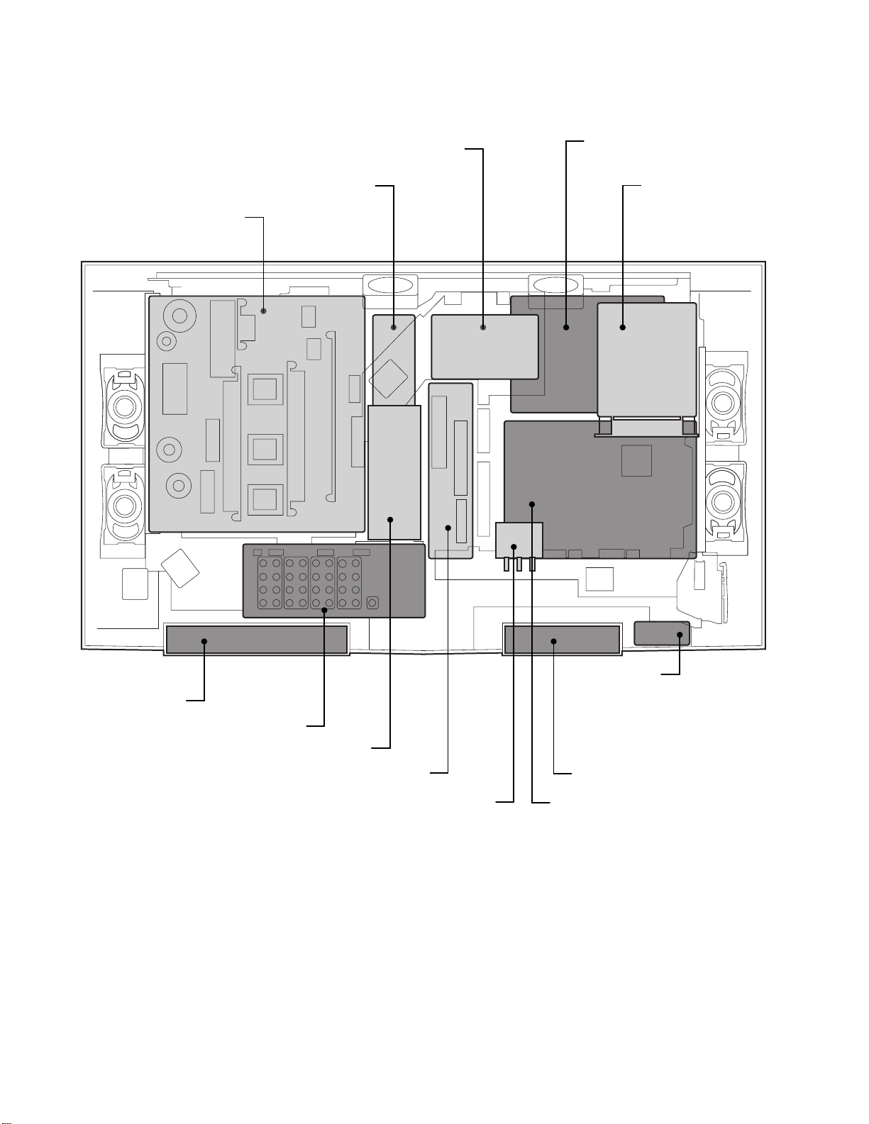
LAYOUT OF MAJOR BOARDS
SWG POWER Module
A-OUT Board
DD POWER Module G-HYPER Module
SCALER &
OSD/MICON Module
GENERAL ADJUSTMENTS
SPECIFIC INFORMATIONS
FRONT/AV Board
BACK/AV Board
DVI Board
TIF-MA Board
RF SW Module
– 9 –
LED/RMT Board
KEY Board
SIGNAL Board
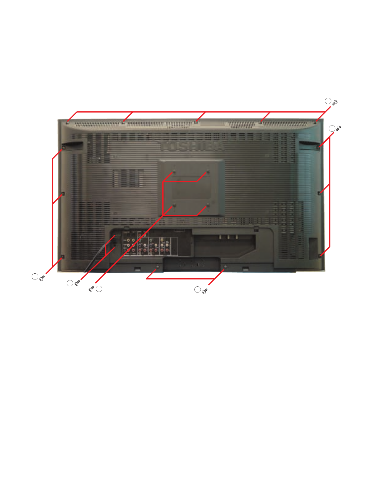
MECHANICAL DISASSEMBLY
R Removing the rear cover
Note: Be sure to lay down the main body (by placing its screen downward) for disassembling.
*
• Remove 13 screws (A).
• Remove 4 screws (B).
A
A
SPECIFIC INFORMATIONS
A
A
B
A
– 10 –
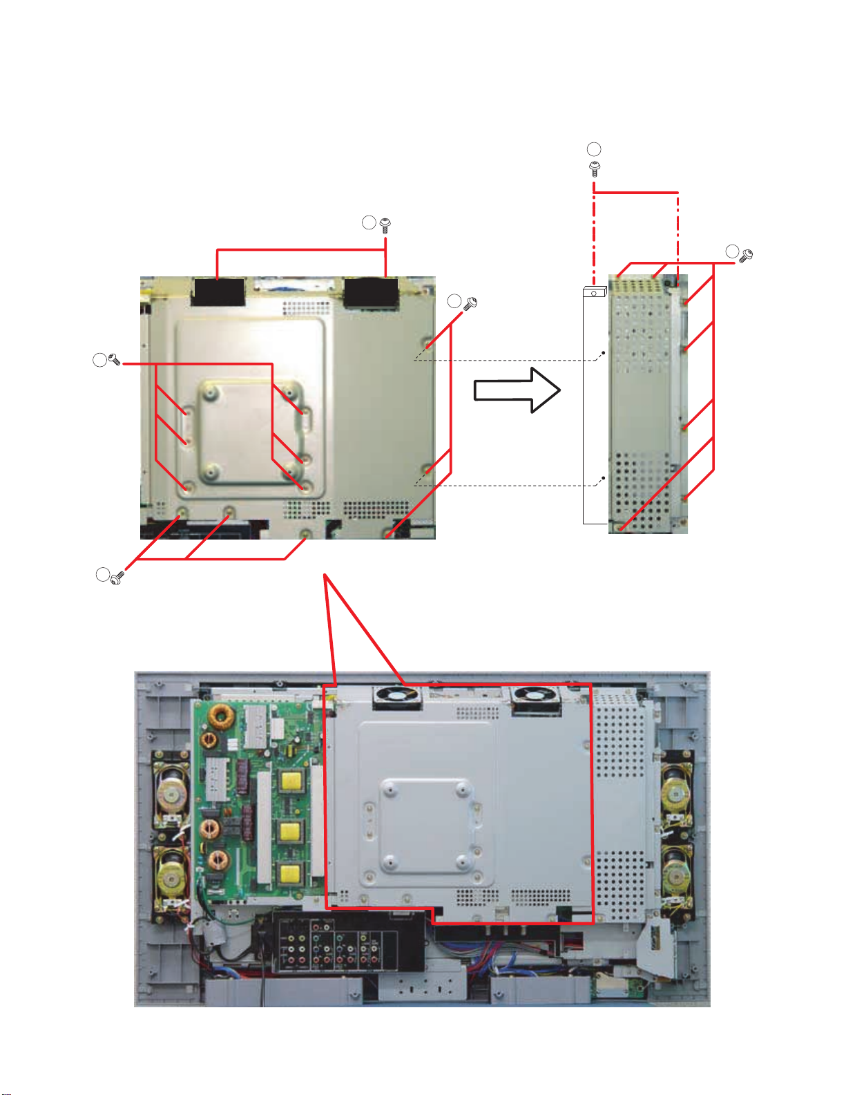
R Removing the brackets
• Remove 14 screws (C).
• Remove 7 screws (D) and 2 screws (E).
E
C
D
C
GENERAL ADJUSTMENTS
C
SPECIFIC INFORMATIONS
C
– 11 –

R Removing the brackets
• Remove flexible wire.
• Disconnect the 60P connector.
SPECIFIC INFORMATIONS
60P connector
G-HYPER Module
Push
– 12 –

R Removing the A-OUT board
• Remove 3 screws (F).
F
A-OUT Board
GENERAL ADJUSTMENTS
SPECIFIC INFORMATIONS
– 13 –
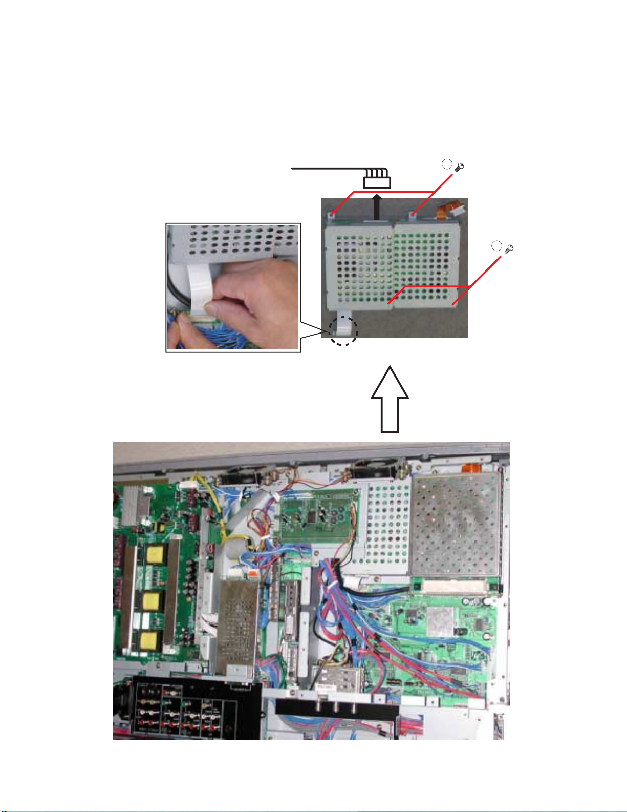
R Removing the SCALER & OSD/MICON module
• Remove 4 screws (G).
• Remove 3 connectors.
SPECIFIC INFORMATIONS
Disconnect
Disconnect
G
G
– 14 –

R Removing the SIGNAL board
• Remove 4 screws (H) on the SIGNAL board.
H
GENERAL ADJUSTMENTS
SIGNAL Board
SPECIFIC INFORMATIONS
– 15 –
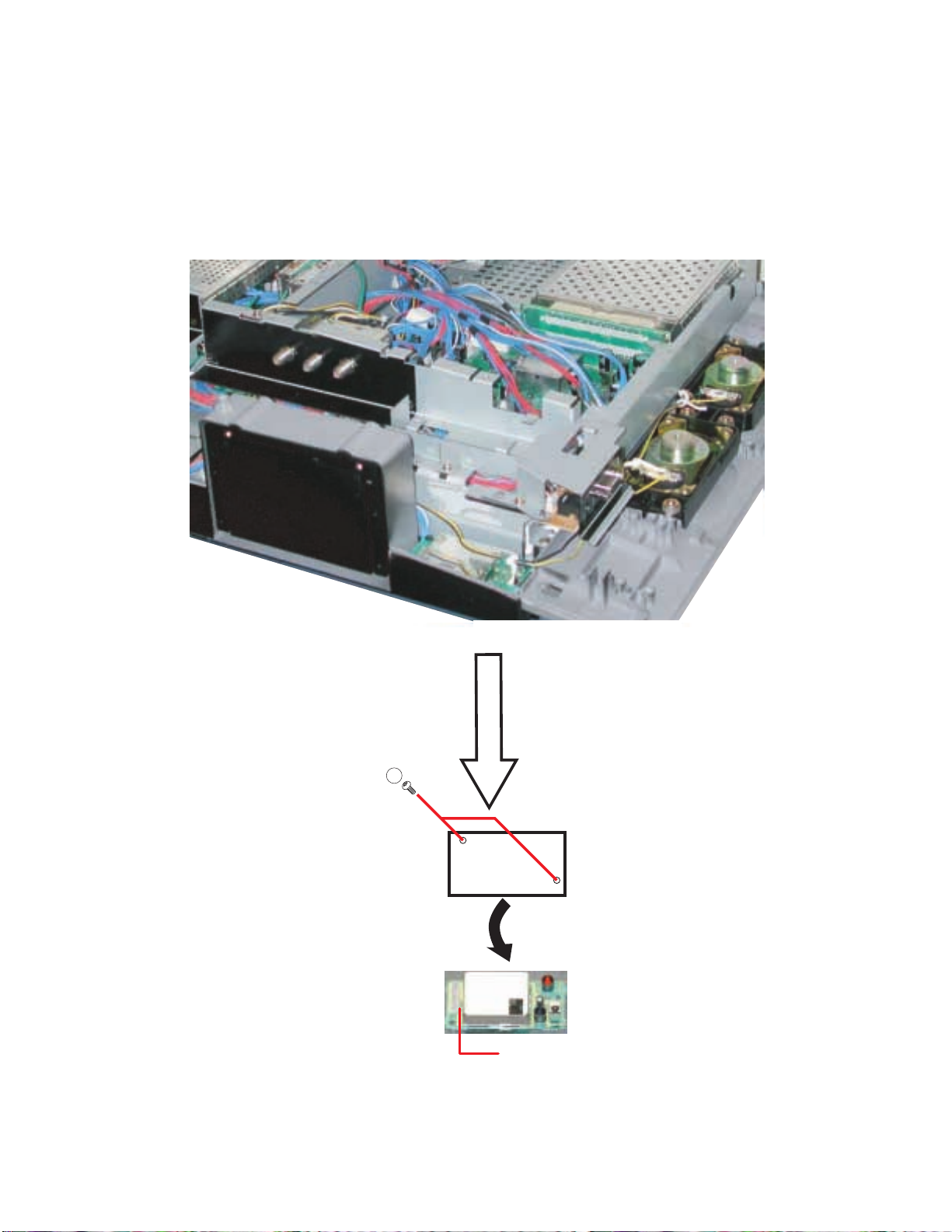
R Removing the LED/RMT board & POW SW board
• Remove 2 screws (J) on the LED/RMT board.
• Remove 4 screws (K) on the POW SW board.
SPECIFIC INFORMATIONS
J
LED/RMT Board
– 16 –
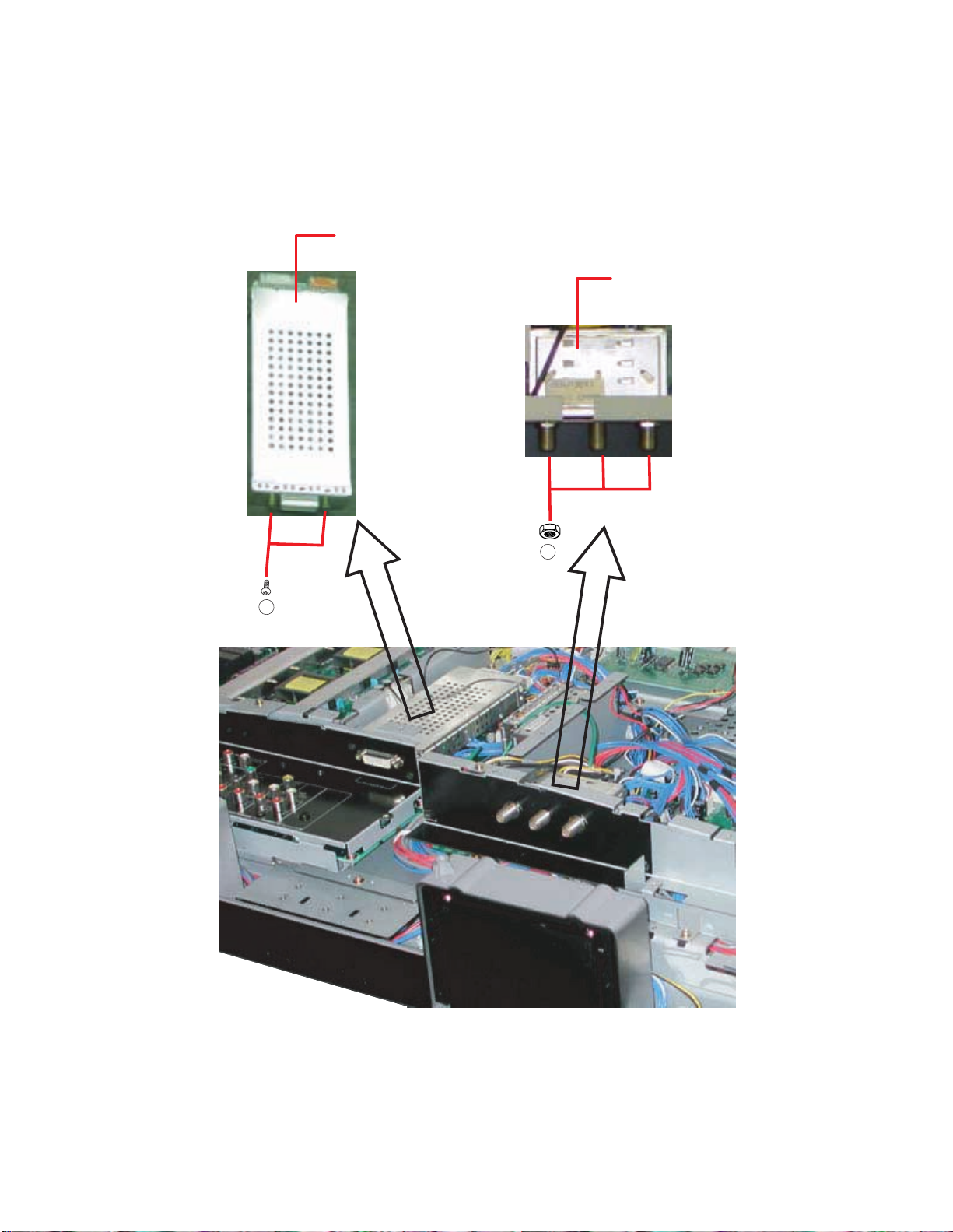
R Removing the DVI unit & RF SW module
• Remove 2 screws (L) to detach the DVI unit.
• Remove 3 nuts (M) fixing the RF SW module.
DVI Unit
RF SW Module
GENERAL ADJUSTMENTS
M
SPECIFIC INFORMATIONS
L
– 17 –
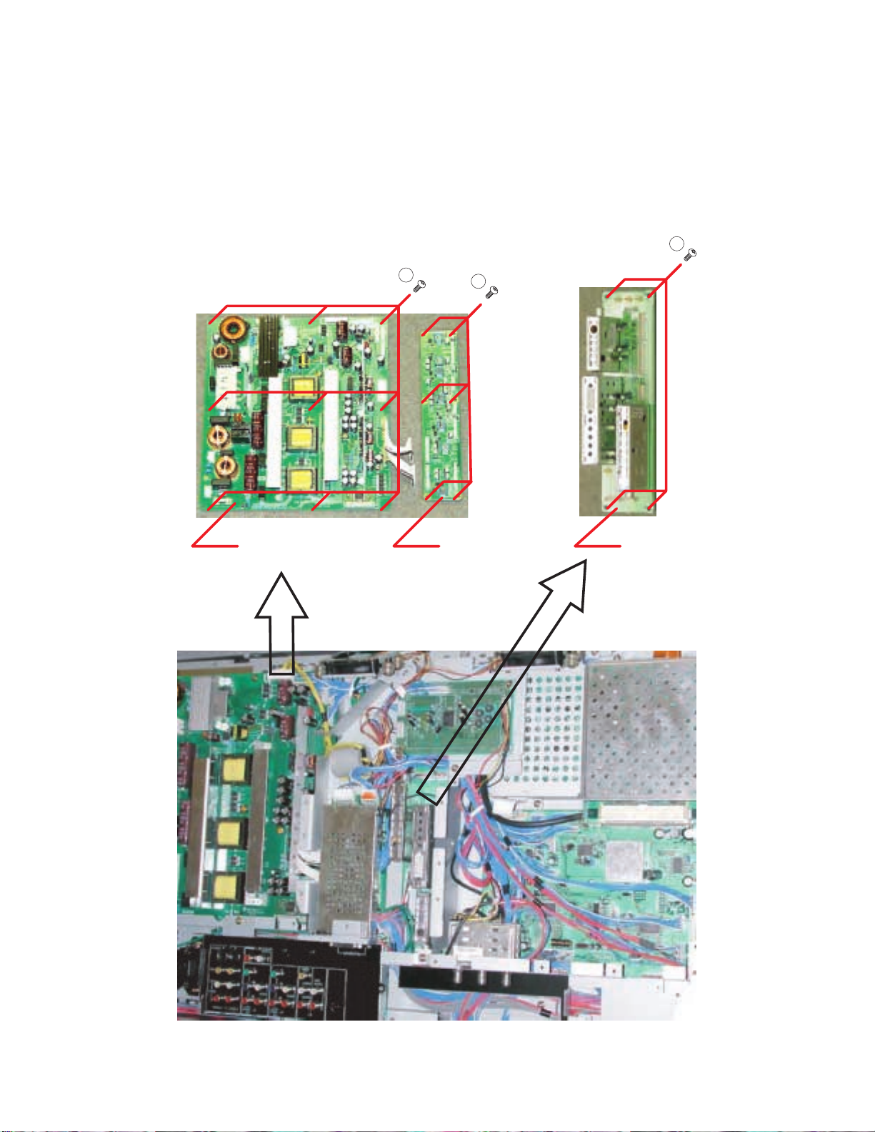
R Removing the SWG POWER/DD POWER module & TIF-MA board
• Remove 9 screws (O) ON THE SWG POWER module.
• Remove 6 screws (P) on the DD POWER module.
• Remove 4 screws (Q) on the TIF-MA board.
Q
SPECIFIC INFORMATIONS
SWG POWER
Module
O
P
DD POWER
Module
TIF-MA
Board
– 18 –
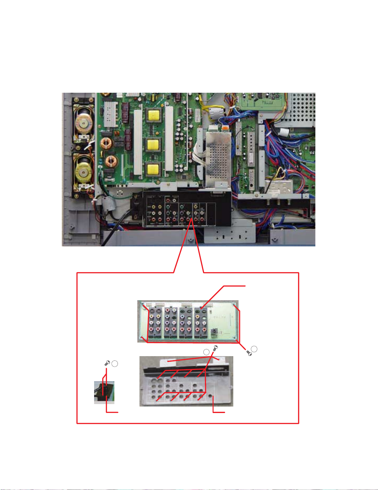
R Removing the BACK/AV board
• Remove 2 screws (R) fixing the AC cord bushing.
• Remove 10 screws (S) on the BACK/AV panel.
• Remove 4 screws (T) on the BACK/AV board.
GENERAL ADJUSTMENTS
SPECIFIC INFORMATIONS
S
R
AC Cord Bushing BACK/IN Panel
BACK/AV Board
T
– 19 –
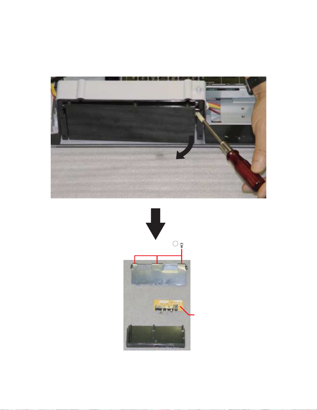
R Removing the FRONT/AV board
• Open the FRONT/AV board holder.
• Remove 3 screws (U).
SPECIFIC INFORMATIONS
OPEN
U
FRONT/AV Board
– 20 –
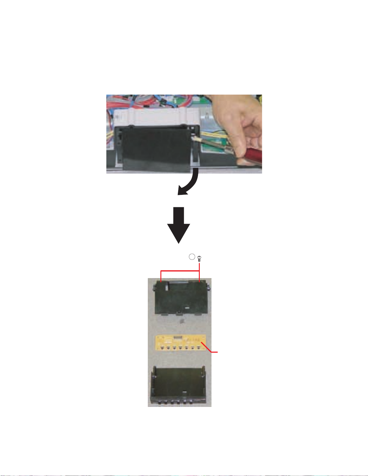
R Removing the KEY board
• Open the KEY board holder.
• Remove 2 screws (V).
GENERAL ADJUSTMENTS
OPEN
SPECIFIC INFORMATIONS
V
KEY Board
– 21 –

R Removing the chassis block
• Remove 15 screws (W).
W W
W
SPECIFIC INFORMATIONS
W
W
– 22 –
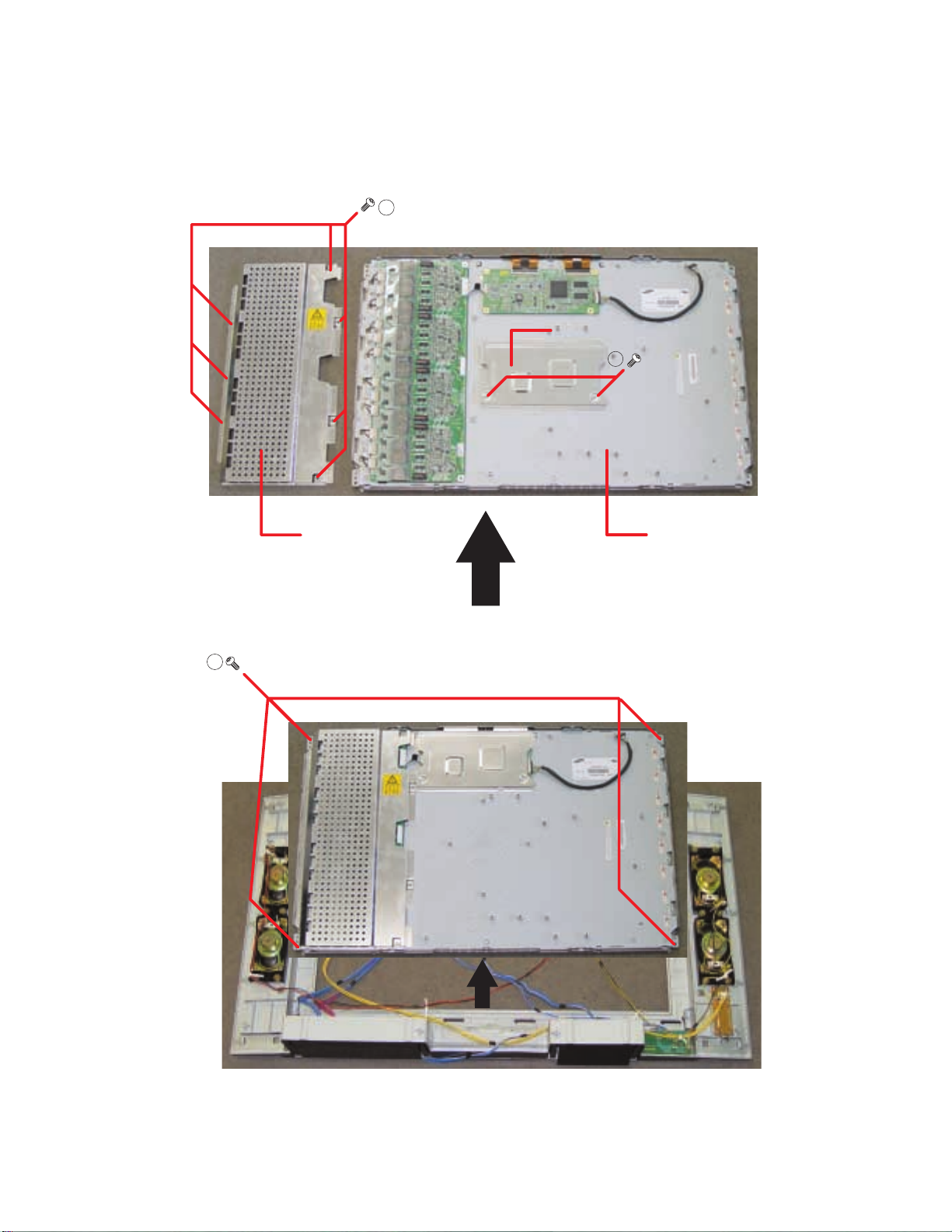
R Removing the LCD block
• Remove 4 screws (X).
W
Shield Case
Y
Shield Case LCD Block
GENERAL ADJUSTMENTS
SPECIFIC INFORMATIONS
X
– 23 –
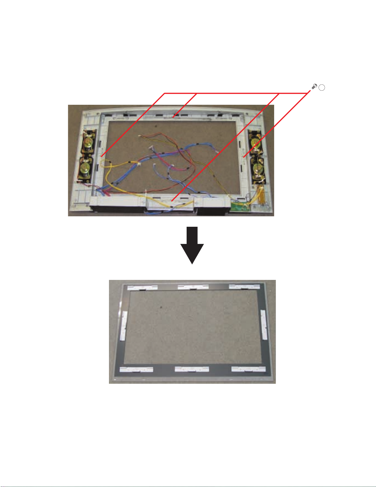
R Removing the front panel
• Remove 4 screws (Z).
SPECIFIC INFORMATIONS
Z
– 24 –
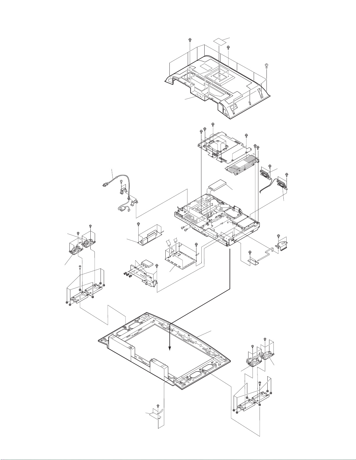
A201
A207
GENERAL ADJUSTMENTS
W661
W662
P801
U001A
UF01
XH02
UF01
SPECIFIC INFORMATIONS
U001B
A101
U002C
– 25 –
W662
W661
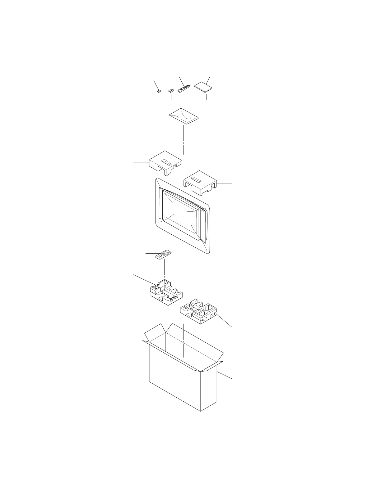
PACKING DISASSEMBLY
SPECIFIC INFORMATIONS
A401
Power code
Y170
K902 Y101
A401
A401
A401
A406
– 26 –
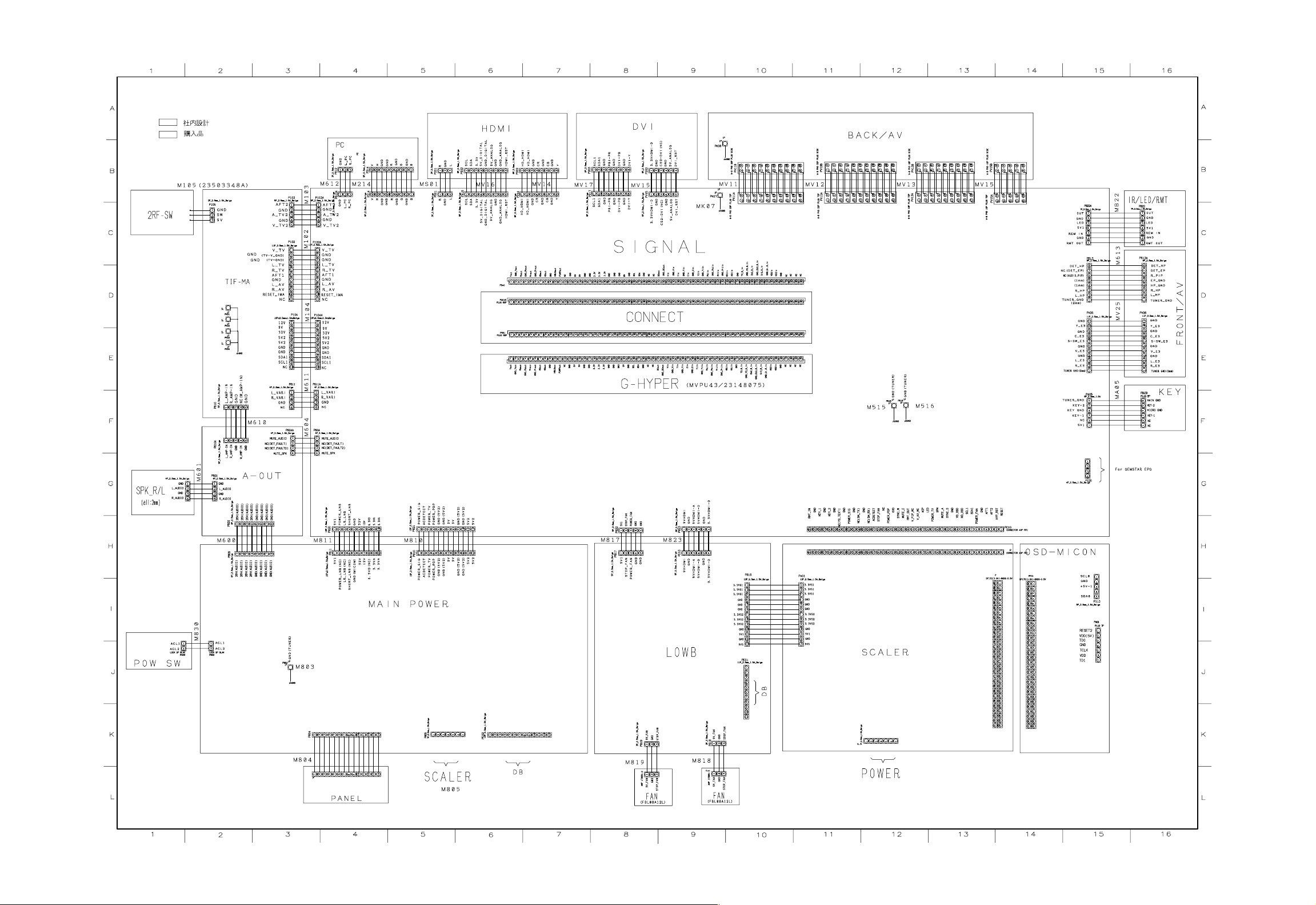
WIRING CONNECTION DIAGRAM
∗ In case where it is indistinct or hard to read, please refer to the attached Circuit Diagram (A1 size).
– 27 – – 28 –

THIS PAGE IS
INTENTIONALLY LEFT
BLANK.
– 29 –
– 30 –
CHASSIS AND CABINET REPLACEMENT PARTS LIST
WARNING: BEFORE SERVICING THIS CHASSIS, READ THE “X-RAY RADIATION PRECAUTION”, “SAFETY PRE-
CAUTION” AND “PRODUCT SAFETY NOTICE” ON PAGE 3 OF THIS MANUAL.
CAUTION: The international hazard symbols “ ” in the schematic diagram and the parts list designate com-ponents
which have special characteristics important for safety and should be replaced only with types identical to those in the
original circuit or specified in the parts list. The mounting position of replacements is to be identical with originals.
Before replacing any of these components, read carefully the PRODUCT SAFETY NOTICE. Do not degrade the
safety of the receiver through improper servicing.
NOTICE:
•
The part number must be used when ordering parts, in order to assist in processing, be sure to include the Model
number and Description.
•
The PC board assembly with * mark is no longer available after the end of the production.
Model : 26HL83
Capacitors ............. CD : Ceramic Disk PF : Plastic Film EL : Electrolytic
Resistors ............... CF : Carbon Film CC : Carbon Composition MF : Metal Film
OMF : Oxide Metal Film VR : Variable Resistor FR : Fusible Resistor
(All CD and PF capacitors are ±5%, 50V and all resistors, ±5%, 1/6W unless otherwise noted.)
Location
Parts No. Description
No.
CAPACITORS
C102 24793221 ELECTROLYTIC, 10V 220UF M
C103 24109102 CERAMIC CHIP, 50V B 1000PF K
C104 24797479 ELECTROLYTIC, 50V 4.7UF M
C105 24763221 ELECTROLYTIC, 16V 220UF M
C108 24793221 ELECTROLYTIC, 10V 220UF M
C122 24092730 CERAMIC CHIP, 16V B 0.1UF K
C124 24109471 CERAMIC CHIP, 50V B 470PF K
C126 24109471 CERAMIC CHIP, 50V B 470PF K
C127 24763101 ELECTROLYTIC, 16V 100UF M
C131 24793221 ELECTROLYTIC, 10V 220UF M
C132 24763101 ELECTROLYTIC, 16V 100UF M
C133 24109102 CERAMIC CHIP, 50V B 1000PF K
C161 24109472 CERAMIC CHIP, 50V B 4700PF K
C162 24109472 CERAMIC CHIP, 50V B 4700PF K
C172 24669339 ELECTROLYTIC, 50V 3.3UF M
C522 24100104 CERAMIC CHIP, 25V F 0.1UF Z
C523 24100104 CERAMIC CHIP, 25V F 0.1UF Z
C524 24100104 CERAMIC CHIP, 25V F 0.1UF Z
C601 24092730 CERAMIC CHIP, 16V B 0.1UF K
C602 24109331 CERAMIC CHIP, 50V B 330PF K
C603 24092730 CERAMIC CHIP, 16V B 0.1UF K
C604 24092611 CERAMIC CHIP, 6.3V B 2.2UF K
C605 24109102 CERAMIC CHIP, 50V B 1000PF K
C606 24109102 CERAMIC CHIP, 50V B 1000PF K
C608 24092730 CERAMIC CHIP, 16V B 0.1UF K
C610 24797010 ELECTROLYTIC, 50V 1UF M
C611 24092730 CERAMIC CHIP, 16V B 0.1UF K
C612 24761102 ELECTROLYTIC, 6.3V 1000UF M
C613 24797010 ELECTROLYTIC, 50V 1UF M
C614 24092730 CERAMIC CHIP, 16V B 0.1UF K
C615 24763101 ELECTROLYTIC, 16V 100UF M
C620 24092463 CERAMIC CHIP, 16V B 0.22UF K
C621 24092730 CERAMIC CHIP, 16V B 0.1UF K
C622 24092463 CERAMIC CHIP, 16V B 0.22UF K
C623 24092463 CERAMIC CHIP, 16V B 0.22UF K
C624 24092730 CERAMIC CHIP, 16V B 0.1UF K
C625 24092463 CERAMIC CHIP, 16V B 0.22UF K
C627 24092730 CERAMIC CHIP, 16V B 0.1UF K
Location
Parts No. Description
No.
C629 24797010 ELECTROLYTIC, 50V 1UF M
C630 24092730 CERAMIC CHIP, 16V B 0.1UF K
C631 24092463 CERAMIC CHIP, 16V B 0.22UF K
C632 24092463 CERAMIC CHIP, 16V B 0.22UF K
C635 24763221 ELECTROLYTIC, 16V 220UF M
C636 24763221 ELECTROLYTIC, 16V 220UF M
C640 24794102 ELECTROLYTIC, 16V 1000UF M
C641 24794470 ELECTROLYTIC, 16V 47UF M
C642 24794470 ELECTROLYTIC, 16V 47UF M
C645 24815103 CERAMIC CHIP, 50V B 10000PF K
C646 24092738 CERAMIC CHIP, 25V B 0.47UF K
C647 24092738 CERAMIC CHIP, 25V B 0.47UF K
C648 24285104 CERAMIC CHIP, 50V B 0.1UF K
C649 24285104 CERAMIC CHIP, 50V B 0.1UF K
C653 24797010 ELECTROLYTIC, 50V 1UF M
C659 24591102 PLASTIC FILM, 50V 1000PF J
C661 24109102 CERAMIC CHIP, 50V B 1000PF K
C662 24109102 CERAMIC CHIP, 50V B 1000PF K
C663 24206108 ELECTROLYTIC, 50V 0.1UF M 7L 3A
C665 24797339 ELECTROLYTIO, 50V 3.3UF M
C666 24797339 ELECTROLYTIO, 50V 3.3UF M
C667 24797478 ELECTROLYTIC, 50V 0.47UF M
C668 24797478 ELECTROLYTIC, 50V 0.47UF M
C669 24105221 CERAMIC CHIP, 50V CH 220PF J
C672 24797229 ELECTROLYTIC, 50V 2.2UF M
C673 24669229 ELECTROLYTIC, 50V 2.2UF M 3A
C677 24109681 CERAMIC CHIP, 50V B 680PF K
C678 24109681 CERAMIC CHIP, 50V B 680PF K
C679 24105221 CERAMIC CHIP, 50V CH 220PF J
C691 24109103 CERAMIC CHIP, 50V B 0.01UF K
C692 24109103 CERAMIC CHIP, 50V B 0.01UF K
C693 24109103 CERAMIC CHIP, 50V B 0.01UF K
C694 24109103 CERAMIC CHIP, 50V B 0.01UF K
C927 24092730 CERAMIC CHIP, 16V B 0.1UF K
C3301 24092538 CERAMIC CHIP, 10V F 1UF Z
C3302 24105102 CERAMIC CHIP, 25V CH 1000PF J
C3303 24092730 CERAMIC CHIP, 16V B 0.1UF K
C3304 24105471 CERAMIC CHIP, 50V CH 470PF J
C4702 24109223 CERAMIC CHIP, 25V B 0.022UF K
SPECIFIC INFORMATIONS
– 31 –

Location
SPECIFIC INFORMATIONS
Parts No. Description
No.
C4703 24073082 ELECTROLYTIC, 50V 2.2UF M 3A
C4704 24092753 CERAMIC CHIP, 10V B 0.22UF K
C4705 24073082 ELECTROLYTIC, 50V 2.2UF M 3A
C4706 24109221 CERAMIC CHIP, 50V B 220PF K
C4707 24092730 CERAMIC CHIP, 16V B 0.1UF K
C4708 24073041 ELECTROLYTIC, 16V 470UF M 3A
C4709 24109103 CERAMIC CHIP, 50V B 0.01UF K
C4710 24109103 CERAMIC CHIP, 50V B 0.01UF K
C4711 24109103 CERAMIC CHIP, 50V B 0.01UF K
C4712 24109103 CERAMIC CHIP, 50V B 0.01UF K
C4713 24109103 CERAMIC CHIP, 50V B 0.01UF K
C4714 24109103 CERAMIC CHIP, 50V B 0.01UF K
C4715 24109103 CERAMIC CHIP, 50V B 0.01UF K
C4716 24092730 CERAMIC CHIP, 16V B 0.1UF K
C4717 24073038 ELECTROLYTIC, 16V 100UF M 3A
CB01 24794470 ELECTROLYTIC, 16V 47UF M
CB40 24092538 CERAMIC CHIP, 10V F 1UF Z
CB41 24109222 CERAMIC CHIP, 50V B 2200PF K
CB42 24105561 CERAMIC CHIP, 50V CH 560PF J
CB43 24109332 CERAMIC CHIP, 50V B 3300PF K
CB45 24092538 CERAMIC CHIP, 10V F 1UF Z
CB46 24109222 CERAMIC CHIP, 50V B 2200PF K
CB47 24105561 CERAMIC CHIP, 50V CH 560PF J
CB51 24590103 PLASTIC FILM, 50V 0.01UF J
CB52 24794470 ELECTROLYTIC, 16V 47UF M
CB53 24503041 PLASTIC FILM , 63V 0.1UF J
CB54 24109221 CERAMIC CHIP, 50V B 220PF K
CB55 24797010 ELECTROLYTIC, 50V 1UF M
CB56 24794470 ELECTROLYTIC, 16V 47UF M
CB59 24590103 PLASTIC FILM, 50V 0.01UF J
CB60 24794100 ELECTROLYTIC, 16V 10UF M
CB61 24503041 PLASTIC FILM , 63V 0.1UF J
CC01 24109102 CERAMIC CHIP, 50V B 1000PF K
CC02 24109102 CERAMIC CHIP, 50V B 1000PF K
CC03 24109102 CERAMIC CHIP, 50V B 1000PF K
CC04 24109102 CERAMIC CHIP, 50V B 1000PF K
CC05 24109102 CERAMIC CHIP, 50V B 1000PF K
CC06 24109102 CERAMIC CHIP, 50V B 1000PF K
CC07 24109102 CERAMIC CHIP, 50V B 1000PF K
CC08 24109102 CERAMIC CHIP, 50V B 1000PF K
CC09 24109102 CERAMIC CHIP, 50V B 1000PF K
CC10 24109102 CERAMIC CHIP, 50V B 1000PF K
CC11 24109102 CERAMIC CHIP, 50V B 1000PF K
CC12 24109102 CERAMIC CHIP, 50V B 1000PF K
CC14 24109102 CERAMIC CHIP, 50V B 1000PF K
CC15 24109102 CERAMIC CHIP, 50V B 1000PF K
CC18 24109102 CERAMIC CHIP, 50V B 1000PF K
CC19 24109102 CERAMIC CHIP, 50V B 1000PF K
CC77 24105101 CERAMIC CHIP, 50V CH 100PF J
CC78 24105101 CERAMIC CHIP, 50V CH 100PF J
CC99 24591102 PLASTIC FILM, 50V 1000PF J
CS01 24092538 CERAMIC CHIP, 10V F 1UF Z
CS02 24092538 CERAMIC CHIP, 10V F 1UF Z
CS03 24092538 CERAMIC CHIP, 10V F 1UF Z
CS04 24092538 CERAMIC CHIP, 10V F 1UF Z
CS05 24092538 CERAMIC CHIP, 10V F 1UF Z
CS06 24092538 CERAMIC CHIP, 10V F 1UF Z
CS07 24092538 CERAMIC CHIP, 10V F 1UF Z
CS08 24092538 CERAMIC CHIP, 10V F 1UF Z
CS09 24092538 CERAMIC CHIP, 10V F 1UF Z
CS10 24092538 CERAMIC CHIP, 10V F 1UF Z
CS11 24092538 CERAMIC CHIP, 10V F 1UF Z
CS12 24092538 CERAMIC CHIP, 10V F 1UF Z
CS13 24794100 ELECTROLYTIC, 16V 10UF M
CS14 24794100 ELECTROLYTIC, 16V 10UF M
Location
Parts No. Description
No.
CS15 24092726 CERAMIC CHIP CK733B 16V 2,200,000PFK
CS16 24092726 CERAMIC CHIP CK733B 16V 2,200,000PFK
CS20 24669478 ELECTROLYTIC, 50V 0.47UF M 3A
CS21 24797479 ELECTROLYTIC, 50V 4.7UF M
CS22 24797479 ELECTROLYTIC, 50V 4.7UF M
CS23 24092538 CERAMIC CHIP, 10V F 1UF Z
CS24 24092538 CERAMIC CHIP, 10V F 1UF Z
CS25 24763101 ELECTROLYTIC, 16V 100UF M
CS26 24092726 CERAMIC CHIP CK733B 16V 2,200,000PFK
CS27 24092726 CERAMIC CHIP CK733B 16V 2,200,000PFK
CS30 24092726 CERAMIC CHIP CK733B 16V 2,200,000PFK
CS31 24092726 CERAMIC CHIP CK733B 16V 2,200,000PFK
CS34 24206010 ELECTROLYTIC, 50V 1.0UF M 7L 3A
CS35 24206010 ELECTROLYTIC, 50V 1.0UF M 7L 3A
CS39 24206010 ELECTROLYTIC, 50V 1.0UF M 7L 3A
CS51 24203100 ELECTORLYTIC, 16V 10UF M 7L 3A
CS501 24092731 CERAMIC CHIP, 16V B 1UF K
CS502 24092726 CERAMIC CHIP CK733B 16V 2,200,000PFK
CS503 24092731 CERAMIC CHIP, 16V B 1UF K
CS504 24105101 CERAMIC CHIP, 50V CH 100PF J
CS505 24105101 CERAMIC CHIP, 50V CH 100PF J
CS510 24092542 CERAMIC CHIP CK733 B 16V 1.0UF K
CV01 24092621 CERAMIC CHIP, 10V B 1UF K
CV02 24092621 CERAMIC CHIP, 10V B 1UF K
CV03 24092621 CERAMIC CHIP, 10V B 1UF K
CV04 24100104 CERAMIC CHIP, 25V F 0.1UF Z
CV05 24092621 CERAMIC CHIP, 10V B 1UF K
CV06 24092621 CERAMIC CHIP, 10V B 1UF K
CV07 24100104 CERAMIC CHIP, 25V F 0.1UF Z
CV08 24794102 ELECTROLYTIC, 16V 1000UF M
CV09 24092621 CERAMIC CHIP, 10V B 1UF K
CV10 24794100 ELECTROLYTIC, 16V 10UF M
CV11 24092621 CERAMIC CHIP, 10V B 1UF K
CV12 24100104 CERAMIC CHIP, 25V F 0.1UF Z
CV13 24100104 CERAMIC CHIP, 25V F 0.1UF Z
CV14 24092621 CERAMIC CHIP, 10V B 1UF K
CV15 24100104 CERAMIC CHIP, 25V F 0.1UF Z
CV23 24794101 ELECTROLYTIC, 16V 100UF M
CV24 24100104 CERAMIC CHIP, 25V F 0.1UF Z
CV38 24109102 CERAMIC CHIP, 50V B 1000PF K
CV39 24109102 CERAMIC CHIP, 50V B 1000PF K
CV40 24794101 ELECTROLYTIC, 16V 100UF M
CV42 24100104 CERAMIC CHIP, 25V F 0.1UF Z
CV45 24092621 CERAMIC CHIP, 10V B 1UF K
CV46 24092621 CERAMIC CHIP, 10V B 1UF K
CV47 24092621 CERAMIC CHIP, 10V B 1UF K
CV48 24109332 CERAMIC CHIP, 50V B 3300PF K
CV64 24794471 ELECTROLYTIC, 16V 470UF M
CV65 24794101 ELECTROLYTIC, 16V 100UF M
CV66 24100104 CERAMIC CHIP, 25V F 0.1UF Z
CV67 24794100 ELECTROLYTIC, 16V 10UF M
CV68 24100104 CERAMIC CHIP, 25V F 0.1UF Z
CV73 24100104 CERAMIC CHIP, 25V F 0.1UF Z
CV79 24794102 ELECTROLYTIC, 16V 1000UF M
CV80 24793222 ELECTROLYTIC, 10V 2200UF M
CV121 24109103 CERAMIC CHIP, 50V B 0.01UF K
CV201 24203101 ELECTROLYTIC, 16V 100UF M 7L 3A
CV202 24203470 ELECTROLYTIC, 16V 47UF M 7L 3A
CV203 24100104 CERAMIC CHIP, 25V F 0.1UF Z
CV204 24203470 ELECTROLYTIC, 16V 47UF M 7L 3A
CV205 24100104 CERAMIC CHIP, 25V F 0.1UF Z
CV237 24100104 CERAMIC CHIP, 25V F 0.1UF Z
CV238 24109103 CERAMIC CHIP, 50V B 0.01UF K
CV239 24100104 CERAMIC CHIP, 25V F 0.1UF Z
CV243 24203100 ELECTORLYTIC, 16V 10UF M 7L 3A
– 32 –
 Loading...