

Page 1
SERVICE MANUAL
(*1), as indicated by the underlined serial number.
LCD Color Television
22AV733F
Ver. 2.00
This model is classified as a green product
This Service Manual describes replacement parts for the green product. When repairing this
green product, use the part(s) described in this manual and lead-free solder (*2).
For (*1) and (*2), refer to GREEN PRODUCT PROCUREMENT and LEAD-FREE
SOLDER.
© TOSHIBA CORPORATION
Page 2

IMPORTANT NOTICE
WARNING:
You are requested that you shall not modify or alter the information or data
provided herein without prior written consent by Toshiba. Toshiba shall not
be liable to anybody for any damages, losses, expenses or costs, if any,
incurred in connection with or as a result of such modification or alteration.
THE INFORMATION OR DATA HEREIN SHALL BE PROVIDED "AS IS"
WITHOUT ANY WARRANTY OF ANY KIND, EITHER EXPRESS OR IMPLIED
WARRANTY OF MERCHANTABILITY AND FITNESS FOR A PARTICULAR
PURPOSE.
Toshiba shall not be liable for any damages, losses, expenses or costs, if
any, incurred in connection with or as a result of use of any information or
data provided herein.
Page 3
IMPORTANT NOTICE
up windows are limited by
User's Guide
Contents:
Install Autodesk DWF Viewer
Internet Explorer Settings
Operating Environment
Functions Provided on Each Drawing Page
Using with Network
Install Autodesk DWF Viewer
Autodesk DWF Viewer is necessary to view drawings and to activate the functions of this system. Please
download and install.
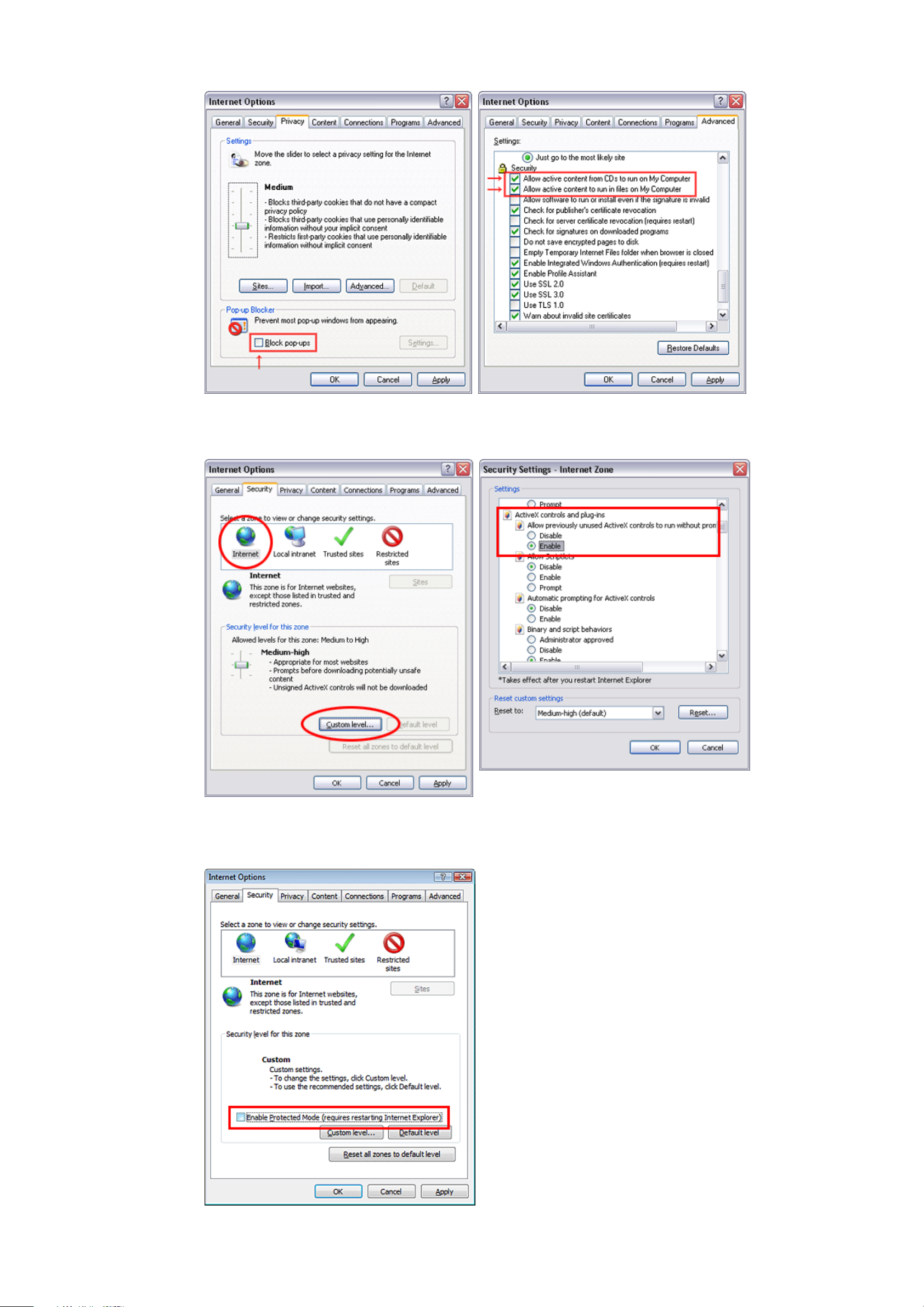
Internet Explorer Settings
When Windows XP SP2 or Windows Vista is used, ActiveX control and pop-
the enhanced security function and this system may not work. In that case, perform the Internet Explorer
setting using the following procedure to restore normal operation.
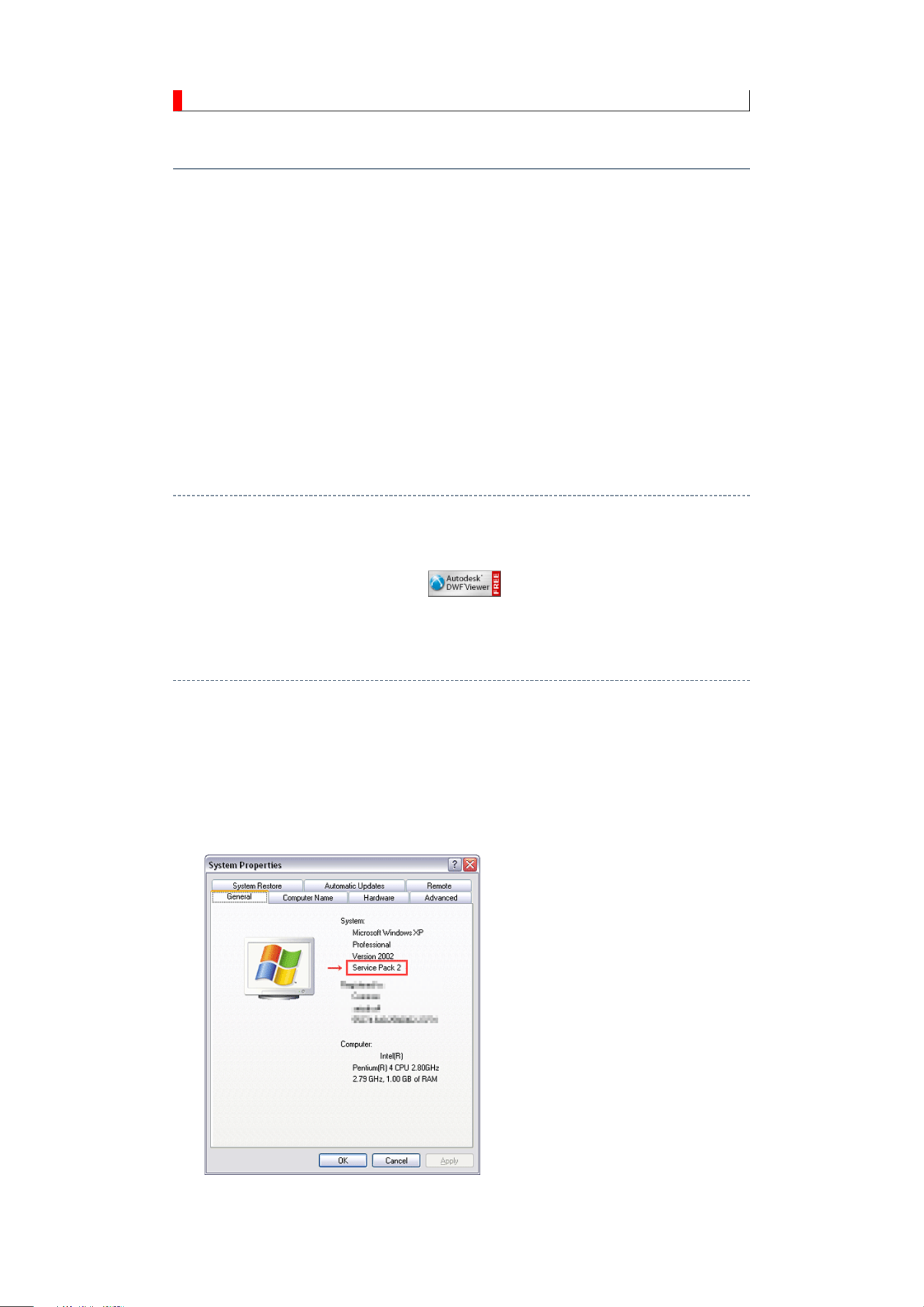
1. Windows version check
[My Computer (right-click)] - [Properties]
2. Internet Explorer setting
[Tools] - [Internet Options]
Page 4
for Internet Explorer 7
for Windows Vista
Page 5

Operating Environment
PC : Pentium III or higher recommended
Monitor : 1024 x 768 or higher resolution recommended
Mouse : A mouse with wheel recommended
OS : Microsoft Windows 2000 SP4 / XP / Vista
Browser : Microsoft Internet Explorer 6.0 / 7.0
Drawing viewer : Autodesk DWF Viewer 6.0 / 7.0
* Use the software following respective license terms and conditions.
Functions Provided on Each Drawing Page
Parts Information Reference Function
When the character string of a part on the drawing is clicked, its information is popped up at the location.
You can get any parts information immediately on the screen without referring to the maintenance parts list.
Parts Search Function
You can search any part within the displayed drawing or within the whole schematic diagram/board view by
specifying a location number. The pop-up window displayed by clicking a part 's character string allows to
search the part within the applicable schematic diagram, board view or spare parts list.
A circle appears when the part is found, showing the part's location within the drawing.
Signal Line/Connector Destination Display Function
When a name at the end of a signal line in a divided schematic diagram is clicked, the destination of the
signal is searched and the display changes to the destination. Connecter destinations can also be searched in
the same way.
When two or more search results are provided, their drawing names are displayed, allowing you to choose a
desired drawing to display.
Layer Display Changing Function
When any of the color buttons on the toolbar is clicked, it can be selected to display desired layer in its color
or not to display each layer. This allows you to see the pattern layer only by setting other layers to "nondisplay".
PC Board View Pattern Highlighting Function
When a pattern on a board view is clicked, it is highlighted in green. This allows easy pattern tracing.
Specified Area Printing Function
The Autodesk DWF Viewer enables to print the displayed drawing region as it is on a printer. It also allows
to print a large-sized drawing in multiple pieces (tile printing).
Using with Network
PRECAUTION
To use ZEUS Service Manual Ver.2 with network, the file-path names written on the source files of each
Page 6
ZEUS Engine Program Ver.2 and ZEUS Service Manual Ver.2 are to be modified.
Perform the procedure described below.
Preparation
1. Run the program file zuesFPch.exe to install the program file for File-Path to the Local PC.
-> Download zeusFPch_setup.zip (2.3MB)
2. Run the program file ZeusSetup_v2.0.exe to install the ZEUS Engine Program in C:\Program
Files\zeus of the local PC. This can be done by running the installer program provided.
3. Create the appropriate folder where the ZEUS Engine Program Ver.2 and the ZEUS Service Manual
Ver.2 to be stored in the server.
4. Move the ZEUS Engine Program of step 2 to the folder created at step 3 in the Server.
5. Detach the ZEUS Service Manual Ver.2 to the folder created at step 3 in the Server.
6. Unzip the ZEUS Service Manual Ver.2 within the folder in the Server.
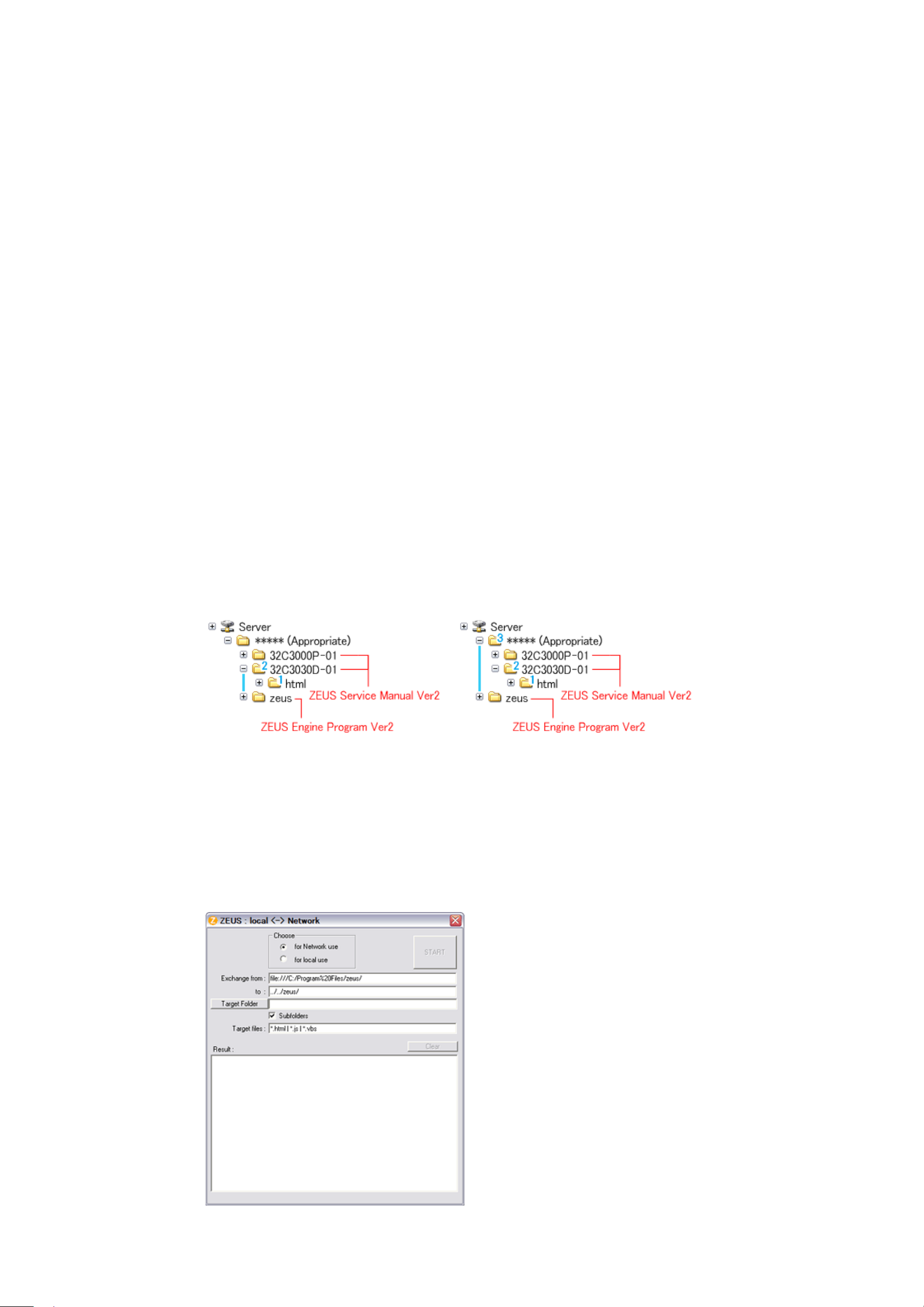
Example of folder
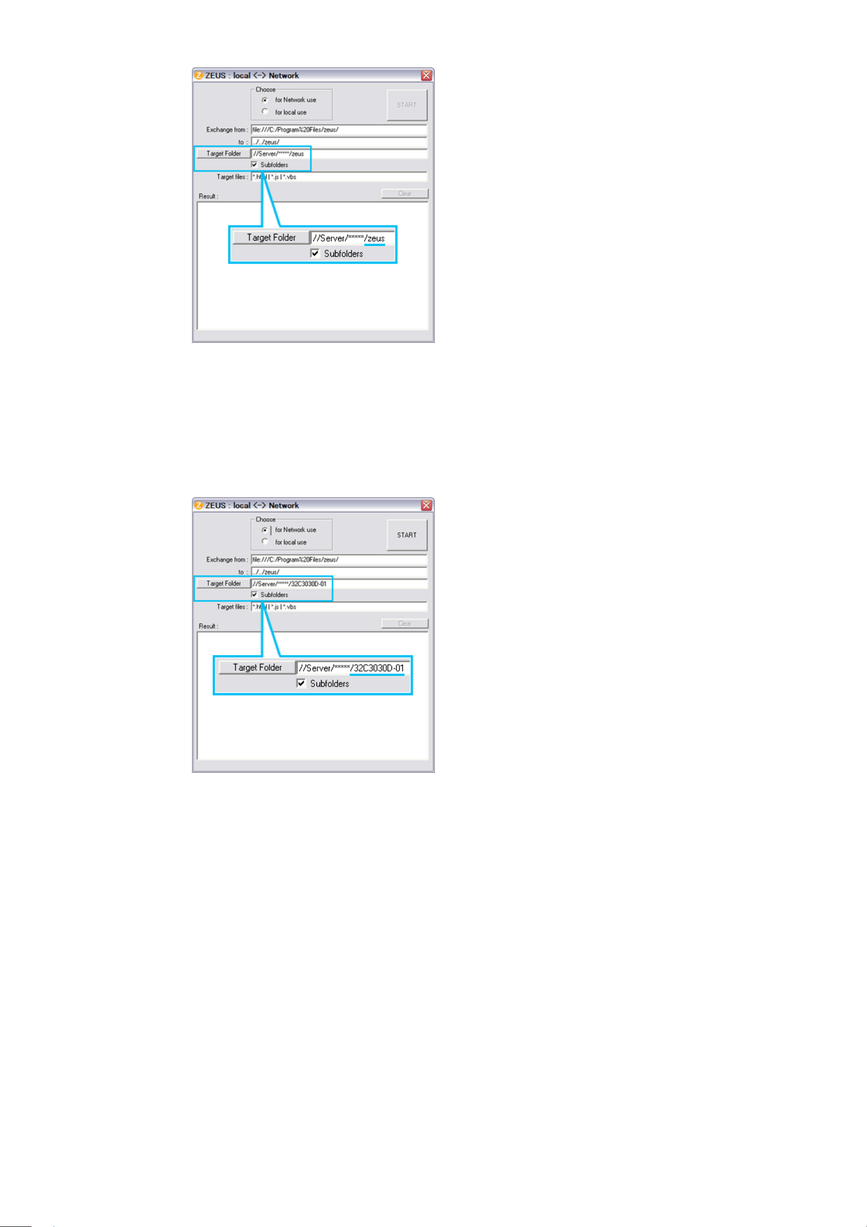
Procedure of File-Path
The zeusFPch is the exclusive program to exchange the file-path names written in both source files of ZEUS
Manual and ZEUS Engine program into those applicable to the network use.
Page 7
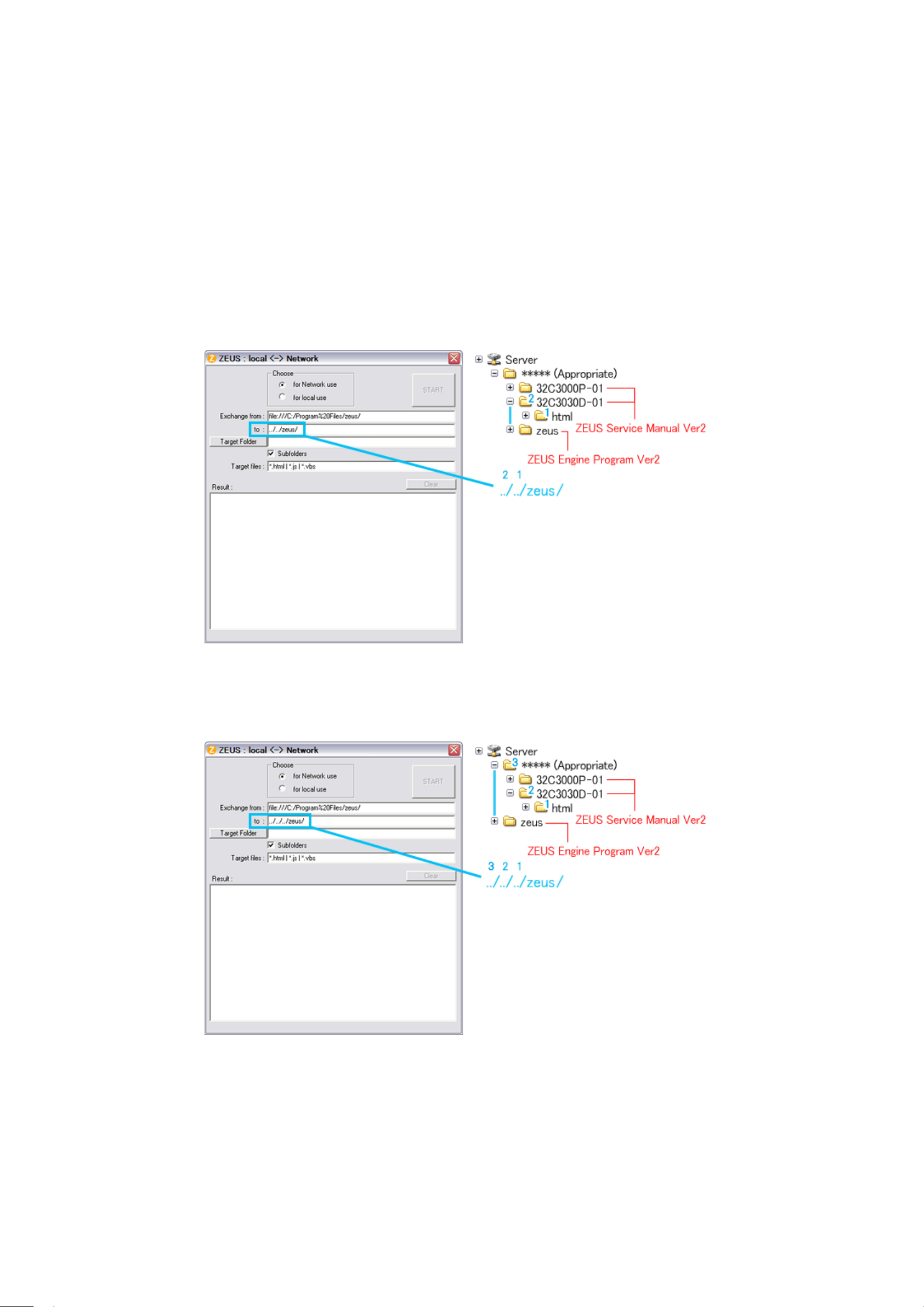
1. Whenever changing the file-
path of both ZEUS Engine Program and ZEUS Service Manual to use with
network, pay the attention to set the "Exchange to" column that should have a proper relation between
ZEUS Engine Program and ZEUS Service Manual with referring the following.
Run the zeusFPch and set "Exchange to" by referring to the examples below.
Example 1 :
In the "Exchange to" column shows the relation between ZEUS Service Manual and ZEUS Engine
Program.
../ counts the relation between.
Thus in this case, it must be ../../zeus/ (2 counts).
Example 2 :
In this case, it must be ../../../zeus/ (3 counts).
2. Run the zeusFPch to change the path in the ZEUS Engine Program Ver.2.
3. Set ZEUS Engine Program in the created folder in the server to the "Target Folder", and then press
"START".
(This procedure is one time only)
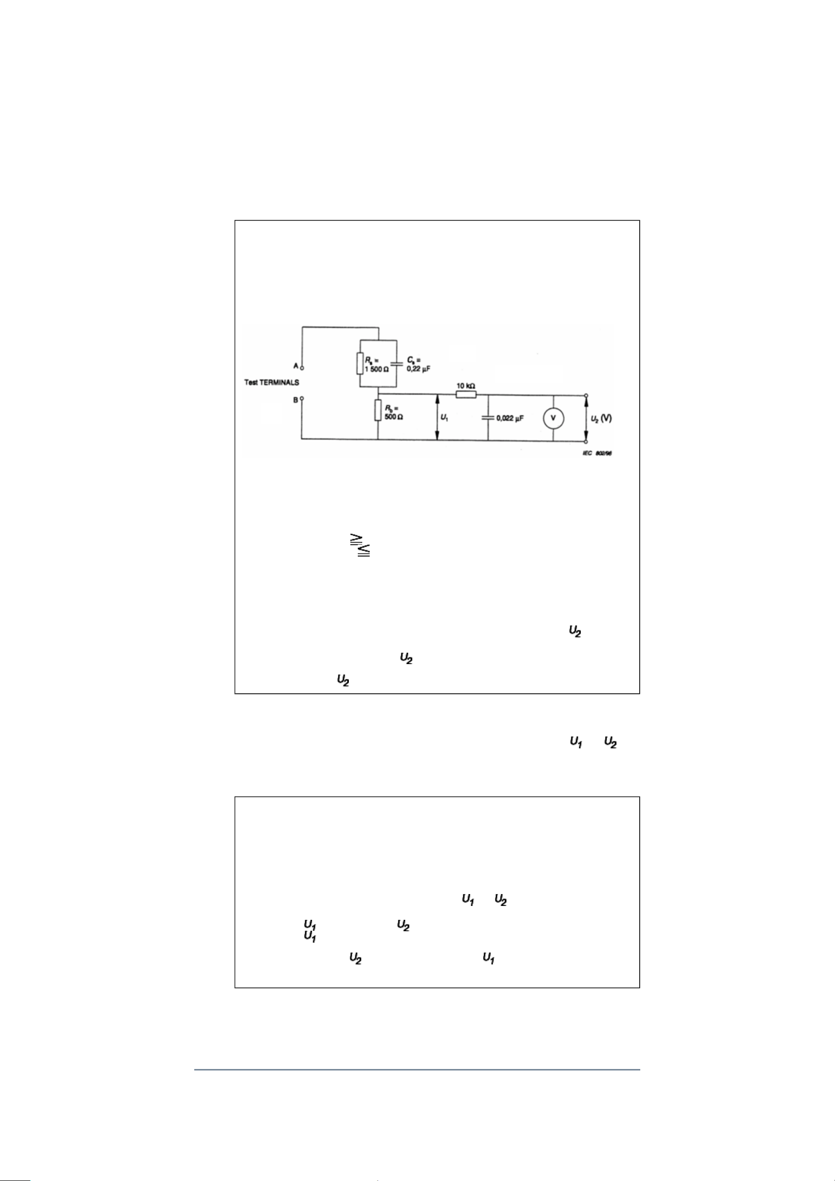
Page 8
4. Run the ZeusFPch to change the path in the ZEUS Service Manual Ver2.
5. Set unzipped ZEUS Service Manual in the created folder in the server to the "Target Folder", and then
press "START".
(This procedure is required whenever placing service manual.)
Confirmation
Confirm that service manual on the server can be operated normally by client PC.
Note:
In case of accessing the ZEUS Manual through WEB site, the small pop-up window appears at the left
bottom corner on the screen whenever searching the location links. This is not malfunction.
Page 9

IMPORTANT NOTICE
Through WEB, ver. 6.5 has been released but with it, the linking function in this manual may
A Known Malfunction
Autodesk® DWF™ Viewer version
(Free software provided through WEB)
Use Autodesk DWF Viewer ver. 6.0.
not work properly.
If ver. 6.5 has been installed, uninstall it and reinstall ver. 6.0.
To get ver. 6.0, click the icon, or contact to the nearest Toshiba Service Centre for further
assistance.
Freezing windows opened
(Cannot close the open windows)
This may happen occasionally.
In case of encountering this, follow the procedure below.
1. Press [Ctrl], [Alt] and [Delete] keys at the same time to engage windows security
windows.
2. Then, choose TASK manager and Application tab, and select TOSHIBA SERVICE
MANUAL-Microsoft Internet Explorer.
3. Click TASK-end.
Main Window back forwarded
The real cause has not been found yet but with this condition, nothing disturbs the service
manual operation.
Continue to use by operating the windows.
Precaution when opening the diagrams
While opening the diagrams, the menu in the left frame changes its color to GRAY. This is
an indication that the viewer is processing.
With this condition, the menu indication color may stick to the GRAY color or Windows
may freeze if clicking other menu.
To avoid such things, do not operate any others while menu turns GRAY color.
If entering this, re-open the service manual or refresh the left frame.
Page 10

GREEN PRODUCT PROCUREMENT
Corporation recognizes environmental protection as a key management tasks, and is doing its
The EC is actively promoting the WEEE & RoHS Directives that define standards for
recycling and reuse of Waste Electrical and Electronic Equipment and for the Restriction of
the use of certain Hazardous Substances. From July 1, 2006, the RoHS Directive will
prohibit any marketing of new products containing the restricted substances.
Increasing attention is given to issues related to the global environmental. Toshiba
utmost to enhance and improve the quality and scope of its environmental activities. In line
with this, Toshiba proactively promotes Green Procurement, and seeks to purchase and use
products, parts and materials that have low environmental impacts.
Green procurement of parts is not only confined to manufacture. The same green parts used
in manufacture must also be used as replacement parts.
Page 11

LEAD-FREE SOLDER
free solder must
free solder may result in damage to the component and or PCB being
This product is manufactured using lead-free solder as a part of a movement within the
consumer products industry at large to be environmentally responsible. Lead-
be used in the servicing and repair of this product.
WARNING: This product is manufactured using lead free solder.
DO NOT USE LEAD BASED SOLDER TO REPAIR THIS PRODUCT!
The melting temperature of lead-free solder is higher than that of leaded solder by 86ºF to
104ºF (30ºC to 40ºC). Use of a soldering iron designed for lead-based solders to repair
product made with lead-
soldered. Great care should be made to ensure high-quality soldering when servicing this
product especially when soldering large components, through-hole pins, and on PCBs as the
level of heat required to melt lead-free solder is high.
Page 12

SAFETY INSTRUCTION
Always keep tools, components of the product, etc away from the children, These items
NEVER remodel the product in any way. Remodeling can result in improper operation,
WARNING: BEFORE SERVICING THIS CHASSIS, READ THE "SAFETY
PRECAUTION" AND "PRODUCT SAFETY NOTICE" INSTRUCTIONS BELOW.
Safety Precaution
WARNING: SERVICING SHOULD NOT BE ATTEMPTED BY ANYONE
UNFAMILIAR WITH THE NECESSARY PRECAUTIONS ON THIS RECEIVER.
THE FOLLOWING ARE THE NECESSARY PRECAUTIONS TO BE OBSERVED
BEFORE SERVICING THIS CHASSIS.
1. An isolation transformer should be connected in the power line between the receiver
and the AC line before any service is performed on the receiver.
2. Always disconnect the power plug before any disassembling of the product. It may
result in electrical shock.
3. When replacing a chassis in the cabinet, always be certain that all the protective
devices are put back in place, such as nonmetallic control knobs, insulating covers,
shields, isolation resistor-capacitor network, etc.
4.
may cause injury to children.
5. Depending on the model, use an isolation transformer or wear suitable gloves when
servicing with the power on, and disconnect the power plug to avoid electrical shock
when replacing parts. In some cases, alternating current is also impressed in the
chassis, so electrical shock is possible if the chassis is contacted with the power on.
6. Always use the replacement parts specified for the particular model when making
repairs. The parts used in products require special safety characteristics such as
inflammability, voltage resistance, etc. therefore, use only replacement parts that have
these same characteristics. Use only the specified parts when the mark is indicated
in the circuit diagram or parts list.
7. Parts mounting and routing dressing of wirings should be the same as that used
originally. For safety purposes, insulating materials such as isolation tube or tape are
sometimes used and printed circuit boards are sometimes mounted floating. Also make
sure that wirings is routed and clamped to avoid parts that generate heat and which use
high voltage. Always follow the manufactured wiring routes / dressings.
8. Always ensure that all internal wirings are in accordance before re-assembling the
external casing after a repairing completed. Do not allow internal wiring to be pinched
by cabinets, panels, etc. Any error in reassembly or wiring can result in electrical
leakage, flame, etc., and may be hazardous.
9.
malfunction, or electrical leakage and flame, which may be hazardous.
Page 13
10. Touch current check. (After completing the work, measure touch current to prevent an
V: Voltmeter or oscilloscope
electric shock.)
Plug the AC cord directly into the AC outlet. Do NOT use an isolation transformer
for this check.
Connect a measuring network for touch currents between each exposed metallic part
on the set and a good earth ground such as a water pipe.
Annex D
(normative)
Measuring network for TOUCH CURRENTS
Resistance values in orms (Ω).
(r.m.s. or peak reading)
Input resistance : 1 MΩ
Input capacitance : 200 pF
Frequency range : 15 Hz to 1 MHz and d.c. respectively
Note: Appropriate measures should be taken to obtain the correct value in case of non
sinusoidal waveforms.
The measuring instrument is calibrated by comparing the frequency factor of with the
solid line in figure F.2 of IEC 60990 at various frequencies. A calibration curve is
constructed showing the deviation of from the ideal curve as a function of frequency.
TOUCH CURRENT = /500 (peak value).
The potential at any point (TOUCH CURRENT) expressed as voltage and
does not exceed the following value:
The part or contact of a TERMINAL is not HAZARDOUS LIVE if:
a) The open-circuit voltage should not exceed 35 V (peak) a.c. or 60 V d.c. or, if a) is not
met.
b) The measurement of the TOUCH CURRENT shall be carried out in accordance with
IEC 60990, with the measuring network described in Annex D of this standard.
The TOUCH CURRENT expressed as voltages and , does not exceed the
following values:
- for a.c. : = 35 V (peak) and = 0.35 V (peak);
- for d.c. : = 1.0 V
Note: The limit values of = 0.35 V (peak) for a.c. and = 1.0 V for d.c. correspond to
the values 0.7 mA (peak) a.c. and 2.0 mA d.c.
Product Safety Notice
Many electrical and mechanical parts in this chassis have special safety-related
Page 14

characteristics. These characteristics are often passed unnoticed by a visual inspection and
the protection afforded by them cannot necessarily be obtained by using replacement
components rated for higher voltage, wattage, etc. Replacement parts which have these
special safety characteristics are identified in this manual and its supplements; electrical
components having such features are identified by the international hazard symbols on the
schematic diagram and the parts list.
Before replacing any of these components, read the parts list in this manual carefully. The
use of substitute replacement parts which do not have the same safety characteristics as
specified in the parts list may create electrical shock, fire, or other hazards.
Page 15
SAFETY INSTRUCTION
should enter the mouth, rinse the mouth thoroughly with water. If the fluid should contact the
When attaching the LCD module to the LCD cover, position it appropriately and fasten
Handling the LCD Module
Safety Precaution
In the event that the screen is damaged or the liquid crystal (fluid) leaks, do not breathe in or
drink this fluid.
Also, never touch this fluid. Such actions could cause toxicity or skin irritation. If this fluid
skin or clothing, wipe off with alcohol, etc., and rinse thoroughly with water. If the fluid
should enter the eyes, immediately rinse the eyes thoroughly with running water.
Precautions for Handling the LCD Module
CAUTION: The metal edges of the LCD module are sharp, handle it with
care.
The LCD module can easily be damaged during disassembly or reassembly; therefore,
always observe the following precautions when handling the module.
1.
at the position where the display can be viewed most conveniently.
2. Carefully align the holes at all four corners of the LCD module with the corresponding
holes in the LCD cover and fasten with screws. Do not strongly push on the module
because any impact can adversely affect the performance. Also use caution when
handling the polarized screen because it can easily be damaged.
3. If the panel surface becomes soiled, wipe with cotton or a soft cloth. If this does not
remove the soiling, breathe on the surface and then wipe again.
If the panel surface is extremely solied, use a CRT cleaner as a cleaner. Wipe off the
panel surface by drop the cleaner on the cloth. Do not drop the cleaner on the panel.
Pay attention not to scratch the panel surface.
4. Leaving water or other fluids on the panel screen for an extended period of time can
Page 16
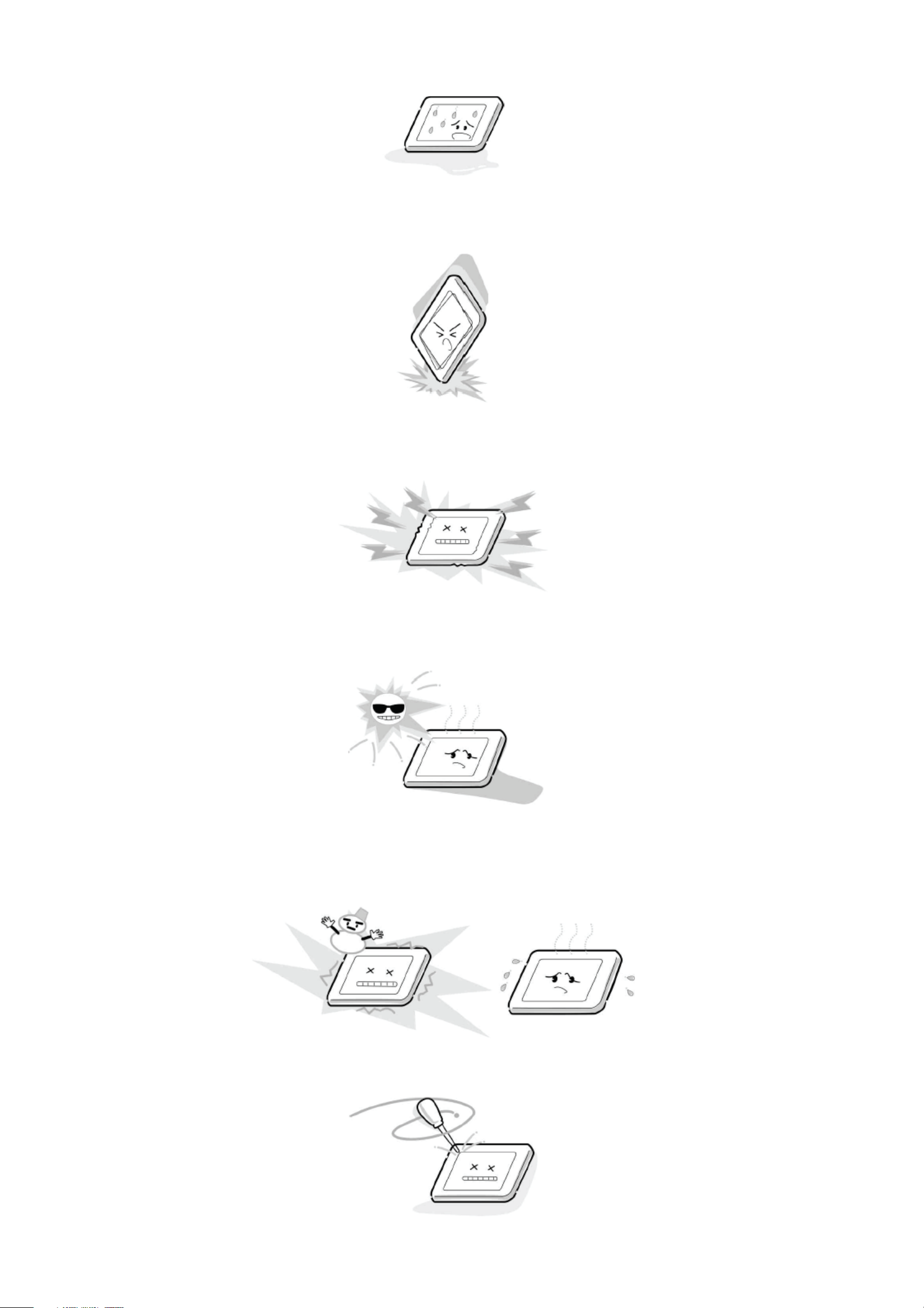
result in discoloration or stripes. Immediately remove any type of fluid from the screen.
5. Glass is used in the panel, so do not drop or strike with hard objects. Such actions can
damage the panel.
6. CMOS-LSI circuitry is used in the LCD module, so avoid damage due to static
electricity. When handling the module, use a wrist ground or anchor ground.
7. Do not expose the LCD module to direct sunlight or strong ultraviolet rays for an
extended period of time.
8. Do not store the LCD module below the temperature conditions described in the
specifications. Failure to do so could result in freezing of the liquid crystal due to cold
air or loss of resilience or other damage.
9. Do not disassemble the LCD module. Such actions could result in improper operation.
Page 17

10. When transporting the LCD module, do not use packing containing epoxy resin
(amine) or silicon resin (alcohol or oxim). The gas generated by these materials can
cause loss of polarity.
Page 18
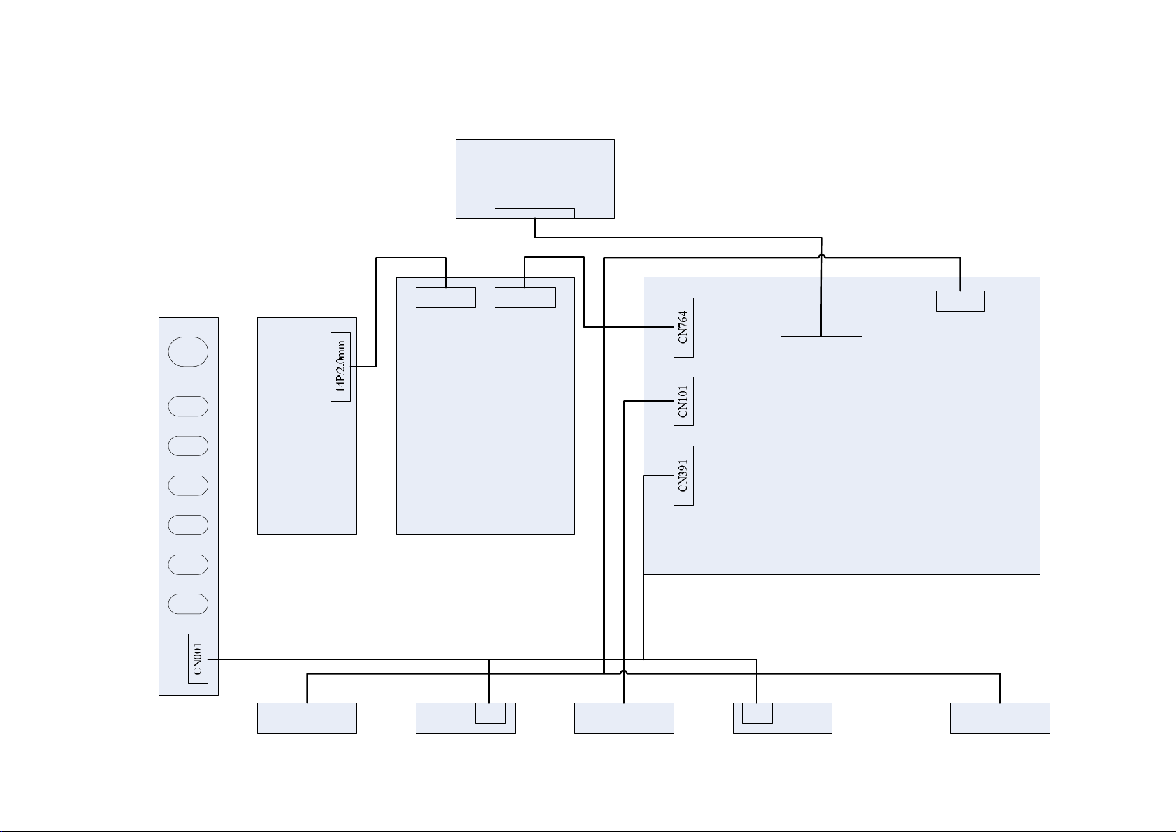
Only for 32"/37"/40"
LCD PANEL
T-COM Board
Main Board
Power Board
CN903 CN902
Inverter
Board
POWER
CH+
CH-
VOL+
VOL-
MENU
SOURCE
CN763
CN501
30P / 1.25mm
SPEAKER SPEAKERIRLOGO LEDLED
CN1CN2
Page 19
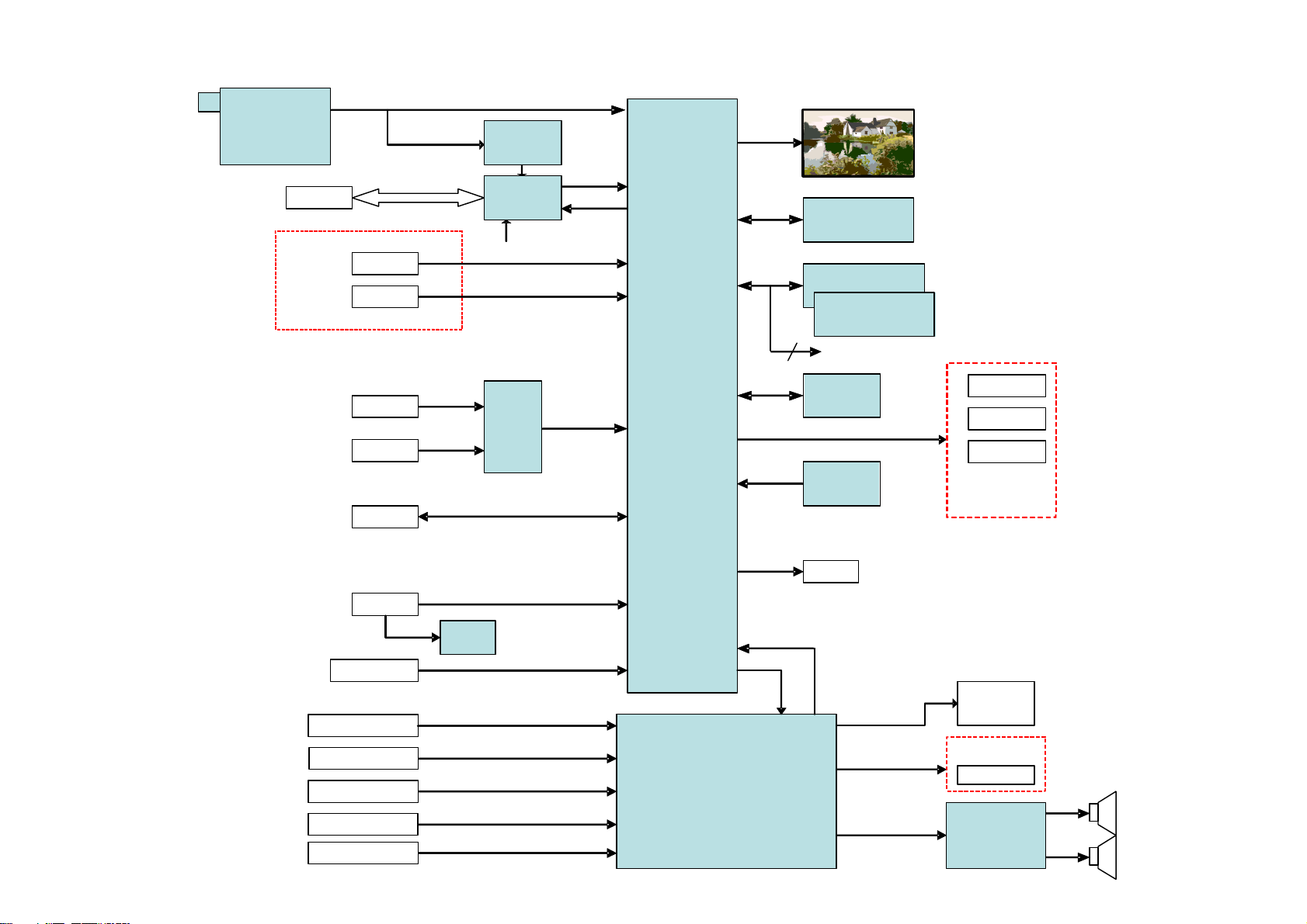
To Panel
U401
SCALER
MT5361B
LQFP256
CVBS
HDMI1
SCART Audio
Component Audio
VGA/HDMI Audio
Side AV Audio
USB
HDMI2
SCART
Component
Side I/O
VGA
U605
Audio Switch
MT8292
ADC OUT R/L
PCMCIA
TS OUT
TS IN
DATA/ADDR
MT8295BN
DAC OUT1
Full In/TV out
IFS P/N
CVBS1
IF P/N TV
TS In
U501
HDMI SW
SiL9187A
19"/22"
3W / 8Ohm
19"/22" WXGA
USB P/M
Rx In
Tx 0-2, Txc
ALX_ARX
PGA2OUT L/R
KEYPAD
IR
LED
KEYPAD/IR
BOARD
SPDIF
Optical
I/O 0_7
I/O 0_7
SY0/SC0
16MB NAND Flash
U405
SPI Flash
512KB NOR
U404
AIN0
AIN
AIN1
CVBS2
DDR2
32MB x 16
U403
AIN_L
AIN_R
AL0_AL2
AR0_AL2
ASPDIF
OSCL0
OSDA0
ORESET#
EEPROM
M24C32
U406
U408
Reset
MAX809ST
IFT P/N
TU103
Tuner
ENV57S01D8F
IFC P/N
U101
DVB-C
Si2163
U102
CI Controller
MT8295BNE
TS Out
U103
EEPROM
M24C02
U602
Sound AMP
TDA8933
HPOL_HPOR
SCART
Audio OUT
SCAR1O L/R
Head Phone
Side I/O
DVD Audio
*Option
Page 20

MAIN BOARD
(715G3747-D)
POWER BOARD
(715G3721)
PANEL
CN803
CN902
CN701CN401CN601
L SPEAKER(2PIN)
R SPEAKER(2PIN)
CN408
PANEL(TCON)
GND11
PS_ON12
ACD10
GND9
GND8
+5V7
+5V6
+16V5
+16V4
N/F3
NC2
DIM1
AC_DETECT10
+ 18 V9
+ 18V8
GND7
GND6
GND5
+5V_STB4
+5V_STB3
BRIGHT_ADJ2
INVERTER_ON_OFF1
GND11
Key112
Key213
GND14
DV33SB10
Light Sensor9
OIRI8
GND7
DV33SB6
LED_POWER
_ON5
LED_POWER
_OFF4
LED_G3
LED_R2
GND1
LOUT+4
LOUT-3
ROUT+2
ROUT-1
C
N
2
0
1
C
N
0
0
1
CN901
AC socket
CN801
KEYBOARD
(715G3957)
IRBOARD
(715G3746)
PANEL_VCC30B0P15
PANEL_VCC29B0N14
PANEL_VCC28A3P13
B3P27A3N12
B3N26CK1P11
GND25CK1N10
GND24GND9
CK2P23GND8
CK2N22A2P7
B2P21A2N6
B2N20A1P5
GND19A1N4
GND18A0P3
B1P17A0N2
B1N16NC1
CN802
CN804
DV33SB4
GND5
RC66
LIGHT_SENSOR7
LED_POWER3
LED_GREEN2
LED_RED1
1 Key1
2 Key2
3 GND
Page 21

SCHEMATIC DIAGRAM
Precaution
WARNING: BEFORE SERVICING THIS CHASSIS, READ THE "X-RAY
RADIATION PRECAUTION" FOR DIRECT VIEW CTV ONLY, "SAFETY
PRECAUTION" AND "PRODUCT SAFETY NOTICE" OF THIS MANUAL.
CAUTION: The international hazard symbols " " in the schematic diagram
and the parts list designate components which have special characteristics
important for safety and should be replaced only with types identical to
those in the original circuit or specified in the parts list.
The mounting position of replacements is to be identical with originals.
Before replacing any of these components, read carefully the SAFETY
PRECAUTION and PRODUCT SAFETY NOTICE.
Do not degrade the safety of the receiver through improper servicing.
Note:
1. RESISTOR
Resistance is shown in ohm [K=1,000, M=1,000,000]. All resistors are 1/6 W and 5 %
tolerance carbon resistor, unless otherwise noted as the following marks.
1/2R : Metal or Metal oxide of 1/2 watt
1/2S : Carbon composition of 1/2 watt
1RF : Fuse resistor of 1 watt
10 W : Cement of 10 watt
K : ±10 %
G : ±2 %
F : ±1 %
2. CAPACITOR
Unless otherwise noted in schematic, all capacitor values less than 1 are expressed in
µF, and the values more than 1 in pF.
All capacitors are ceramic 50 V, unless otherwise noted as the following marks.
= Electrolytic capacitor
= Mylar capacitor
3. The parts indicated with " " have special characteristics, and should be replaced with
identical parts only.
4. Voltages read with DIGITAL MULTI-METER from point indicated to chassis ground,
using a color bar signal with all controls at normal, line voltage at nominal AC volts.
5. Waveforms are taken receiving color bar signal with enough sensitivity.
6. Voltage reading shown are nominal values and may vary ±20 % except H.V.
Page 22

5
5
4
4
3
3
2
2
1
1
D D
C C
B B
A A
OPWRSB
ACD_control
BRIGHT_ADJ
BRIGHT_ADJ
OPWRSB
AC_Detect
OPWRSB
INVERTER_ON_OFF
INVERTER_ON_OFF
ACD_control
AC_Detect
AC_DET
+5V_STB
+5V_STB
DV11
+5V_SW
DV33
+18V
DV11
+18V_A+18V
+5V_STB
DV33SB_E
ACD_control6
BRIGHT_ADJ18
INVERTER_ON_OFF18
OPWRSB6
2K10 TOP BIG SERIAL MODEL MT5361 (LQFP) (DDR1)- 2 LAYERS
DC POWER INPUT
NEARLY U600
BRIGHT_ADJ:
Normal:Max:+3V3, Min:0V
Stand_By:0V
Normal: High
Stand_By:
Low
Vout =1.1V , R108 = 620, R109=1.5K
SMD
NEARLY U105
INVERTER_ON_OFF:
Normal: High
Stand_By: Low
+5V_STB(+5V1) TO +5V_SW BY OPWRSB
OPWRSB(+5V_SW ON/OFF):
Normal: High
Stand_By: Low
Control DV11 and DV33 Sequence
LOW E.S.R
+18V TO +18V_A BY OPWRSB
Vout = 0.8 * (1+R108/R109)
C712NCC712
NC
C708
100N 50V
C708
100N 50V
+
C703
100uF25V
+
C703
100uF25V
R716
620OHM +-5% 1/10W
R716
620OHM +-5% 1/10W
C711NCC711
NC
Q704
Si5403DC-T1-GE3
Q704
Si5403DC-T1-GE3
D
1
D
2
D
3
G4S
5
D
6
D
7
D
8
R704
1K 1/10W
R704
1K 1/10W
R701 0R05 1/10WR701 0R05 1/10W
C704
NC/4.7UF 10V
C704
NC/4.7UF 10V
R702
NC/0 OHM +-5% 1/4W
R702
NC/0 OHM +-5% 1/4W
+
C715
220uF16V
+
C715
220uF16V
C705
2.2uF 10V
C705
2.2uF 10V
C701
0.1uF 50V
C701
0.1uF 50V
R710
10K 1/10W
R710
10K 1/10W
L701
27uH
L701
27uH
C716NCC716
NC
R70368K 1/10W 5% R70368K 1/10W 5%
TP704TP704
1
R709
100R 1/16W 5%
R709
100R 1/16W 5%
R708
NC/0R 1/10W 5%
R708
NC/0R 1/10W 5%
TP703TP703
1
C718
NC/0.1uF 50V
C718
NC/0.1uF 50V
C710
4U7 10V
C710
4U7 10V
R718
1K5 1/10W 5%
R718
1K5 1/10W 5%
CN701
CONN
CN701
CONN
1
2
3
4
5
6
7
8
9
10
C719
4.7UF 10V
C719
4.7UF 10V
R711
47K 1/10W
R711
47K 1/10W
R717
2.7K 1/10W
R717
2.7K 1/10W
+
C706
100UF 16V
+
C706
100UF 16V
C714
1uF 25V
C714
1uF 25V
Q702
AO4419
Q702
AO4419
S
1
S
2
S
3
G
4
D
8
D
7
D
6
D
5
IC702
AP1538SG-13
IC702
AP1538SG-13
FB
1
EN
2
OCSET
3
VCC4OUTPUT
5
OUTPUT
6
VSS
7
VSS
8
R714
7K5 1/10W 5%
R714
7K5 1/10W 5%
D701
SR34
D701
SR34
1 2
Q701
2SK1828
Q701
2SK1828
TP701TP701
1
+
C709
100UF 16V
+
C709
100UF 16V
FB703 220R/2000mAFB703 220R/2000mA
1 2
R706
10K 1/16W 5%
R706
10K 1/16W 5%
+
C702
100uF 25V
+
C702
100uF 25V
Q705
BC847C
Q705
BC847C
3
2
1
Q703
BC847C
Q703
BC847C
3
2
1
R705
22K 1/10W
R705
22K 1/10W
R712
10K 1/10W
R712
10K 1/10W
C707
100N 50V
C707
100N 50V
+
C713
220UF 25V
+
C713
220UF 25V
TP702TP702
1
FB702 220R/2000mAFB702 220R/2000mA
1 2
R713
6K8 1/10W 5%
R713
6K8 1/10W 5%
R707
4K7 1/10W 5%
R707
4K7 1/10W 5%
R715
NC/2.2 OHM 1/10W
R715
NC/2.2 OHM 1/10W
C717
0.1uF 50V
C717
0.1uF 50V
MAIN [3] POWER 1
Page 23

A
A
B
B
C
C
D
D
E
E
4 4
3 3
2 2
1 1
PANEL_VCC_ON/OFF
PANEL_VCC_ON/OFF
+18V_A
AV25
+5V_SW
AV33
+5V_TUNER
DV33
DV33SB
+12V
+5V_SW
AV125
+5V_SW
+5V_SW
DV33
+5V_SW
DV33
+5V_STB
PANEL_VCC
AV25
+5V_STB +5V_STB_E
DV33SB DV33SB_E
PANEL_VCC_ON/OFF6
+5V_TUNER FROM Regulator
SMD/0402
+5V_STB TO DV33SB
Vo=0.5x(R1+R2)/R2
NEARLY TUNER
Vout = 0.8 * (1+R105/R106)
+18V_A TO +12V
DV33 TO AV125
Vout =3.35V , R105= 5.1K, R106=1.6K
NEARLY U605
PANEL_VCC
ON/OFF:MT8295(GPIO10)
Normal:High
Stand_By:Low
FOR Panel VCC 5V
+5V_SW TO AV25
+5V_SW TO DV33
+5V_SW TO AV33
EMI SOLUTION FOLLOW SPECIAL PLACE
Vo=1.25 x (1+120R/120R) = 2.5V
U703 G1117T63UfU703 G1117T63Uf
VIN
3
GND
1
VOUT
2
TH
4
R735
43KOHM +-1% 1/10W
R735
43KOHM +-1% 1/10W
R737
5K1 1/10W 1%
R737
5K1 1/10W 1%
C737
NC/0.1uF 50V
C737
NC/0.1uF 50V
C744
NC/01uF
C744
NC/01uF
FB707
600R/500mA
FB707
600R/500mA
1 2
+
C728
100UF 16V
+
C728
100UF 16V
C727
4.7UF 10V
C727
4.7UF 10V
R721
120R 1% 1/10W
R721
120R 1% 1/10W
IC701
AME5106AIHAADJZ
IC701
AME5106AIHAADJZ
FB
1
EN
2
OCSET
3
IN4SW
5
SW
6
GND
7
GND
8
C734
100N 50V
C734
100N 50V
R731
3.6K 1/10W
R731
3.6K 1/10W
C732
100N 50V
C732
100N 50V
R725
47K 1/10W
R725
47K 1/10W
U702 G1117T63UfU702 G1117T63Uf
VIN
3
GND
1
VOUT
2
TH
4
R722
22K 1/10W
R722
22K 1/10W
C723100N 50V C723100N 50V
R729
0R05 1/4W
R729
0R05 1/4W
R732
NC/2.2 OHM 1/10W
R732
NC/2.2 OHM 1/10W
+
C746 470uF/16V+C746 470uF/16V
R723 22K 1/10WR723 22K 1/10W
+
C731
10uF 50V
+
C731
10uF 50V
C726 NC/470N 10VC726 NC/470N 10V
R720
NC/0R05 1/4W
R720
NC/0R05 1/4W
Q707
BC847C
Q707
BC847C
3
2
1
U706
SC4215HSETRT
U706
SC4215HSETRT
NC
1
EN
2
VIN
3
NC
4
GND
8
FB
7
VO
6
NC
5
TH1
9
+
C721
100uF 10V
+
C721
100uF 10V
+
C733
100UF 16V
+
C733
100UF 16V
C7221uF 25V C7221uF 25V
R733
5K1 1/10W 1%
R733
5K1 1/10W 1%
R736
1.62KOHM 1/10W
R736
1.62KOHM 1/10W
R727 NC/0R05 1/10W 5%R727 NC/0R05 1/10W 5%
C720
100N 50V
C720
100N 50V
U704
G1117-33T43UF
U704
G1117-33T43UF
ADJ(GND)1VOUT(TAB)2VIN
3
C725
10U 10V
C725
10U 10V
C743
0.1uF 50V
C743
0.1uF 50V
R726
120R 1% 1/10W
R726
120R 1% 1/10W
R728
120R 1% 1/10W
R728
120R 1% 1/10W
FB708
600R/500mA
FB708
600R/500mA
1 2
Q706
Si5403DC-T1-GE3
Q706
Si5403DC-T1-GE3
D
1
D
2
D
3
G4S
5
D
6
D
7
D
8
R730
20K 1/10W
R730
20K 1/10W
+
C740
100uF 10V
+
C740
100uF 10V
C739
100N 50V
C739
100N 50V
R724
0R05 1/10W
R724
0R05 1/10W
C741
0.1uF 50V
C741
0.1uF 50V
C745 0.1uF 50VC745 0.1uF 50V
C748
0.1uF 50V
C748
0.1uF 50V
L702 27uHL702 27uH
FB706
NC/220R/2000mA
FB706
NC/220R/2000mA
1 2
C724
100N 50V
C724
100N 50V
+
C738
100uF 10V
+
C738
100uF 10V
C742
100N 50V
C742
100N 50V
U701
AME8810-AEGTZ 0.6A/3.3V
U701
AME8810-AEGTZ 0.6A/3.3V
GND
1
VOUT(heat sink)
2
VIN
3
4
4
C749
0.1uF 50V
C749
0.1uF 50V
R719
0R05 1/4W
R719
0R05 1/4W
D702
SR34
D702
SR34
1 2
FB705
NC/220R/2000mA
FB705
NC/220R/2000mA
1 2
C730
10U 10V
C730
10U 10V
U705
L78L12ABUTR
U705
L78L12ABUTR
IN3OUT
1
GND
2
R734
1.5K +-1% 1/10W
R734
1.5K +-1% 1/10W
C735 NC/0.47uFC735 NC/0.47uF
+
C736
220uF16V
+
C736
220uF16V
C747
NC/1nF 50V
C747
NC/1nF 50V
C729
100N 16V
C729
100N 16V
MAIN [4] POWER 2
Page 24

5
5
4
4
3
3
2
2
1
1
D D
C C
B B
A A
RDQM1
RWE#
RA9
RA1
RA8
RA1
RDQM0
AV12_MEMPLL
RA4
RDQM1
MEM_CLK0
RA7
MEM_CLK0#
RA2
RDQ14
RDQ12
RDQ12
RA9
RA11
RA7
RA5
RDQ6
RA6
RRAS#
RCAS#
RDQ0
RDQ8
RA0
RDQ5
AV12_MEMPLL
RDQ2
RDQM0
RDQ15
RBA0
RDQ8
RDQ3
RDQ7
RA0
RDQS1
MEM_CLK0#
RDQ0
RDQ1
RA6
RDQ10
RA12
RDQS0
RBA0
RRAS#
RCS#
RDQ11
RDQ13
RDQ7
RDQ6
RDQ3
RCLK0
RCAS#
RDQ4
RDQS0
RDQ2
RA3
RCLK0#
RA2
RCKE
RCLK0
RCLK0#
RWE#
RBA1
RDQ13
RCKE
RCS#
RDQ15
RA4
RA3
RA8
RCS#
RDQ9
MEM_CLK0
RDQ9
RDQ4
MEM_VREF
RDQ10
MEM_VREFRA12
RDQ1
MEM_VREF
RDQ11
RDQ14
RBA1
RDQ5
RA10
RA5
RA11
RA10
RDQS1
DDRVDV33
DDRV
DDRV
AV125
DDRV
DDRV
DDRV
DDRV
DDRV
DDRV
Top
Component item from 2xx in this part.
Bottom
Bottom
DRAM
Bottom
DRAM Power
Under MT5361
NEAR IC
Close to C280
LOW E.S.R
R402
110 OHM +-1% 1/10W
R402
110 OHM +-1% 1/10W
C405
NC/100N 16V
C405
NC/100N 16V
C414
4.7UF 10V
C414
4.7UF 10V
C421
100N 16V
C421
100N 16V
R405
NC/1K 1/10W 5%
R405
NC/1K 1/10W 5%
R411
22R 1/16W 5%
R411
22R 1/16W 5%
C417
10N 50V
C417
10N 50V
C404
4.7UF 10V
C404
4.7UF 10V
C402
100N 50V
C402
100N 50V
C422
100N 16V
C422
100N 16V
C418
10U 10V
C418
10U 10V
R404
1K 1/16W
R404
1K 1/16W
C423
100N 16V
C423
100N 16V
U403
NT5TU32M16CG-25C
U403
NT5TU32M16CG-25C
VDD
A1
NC
A2
VSS
A3
VSSQ
A7
UDQS
A8
VDDQ
A9
DQ14
B1
VSSQ
B2
UDM
B3
UDQS
B7
VSSQ
B8
DQ15
B9
VDDQ
C1
DQ9
C2
VDDQ
C3
VDDQ
C7
DQ8
C8
VDDQ
C9
DQ12
D1
VSSQ
D2
DQ11
D3
DQ10
D7
VSSQ
D8
DQ13
D9
VDD
E1
NC
E2
VSS
E3
VSSQ
E7
LDQS
E8
VDDQ
E9
DQ6
F1
VSSQ
F2
LDM
F3
LDQS
F7
VSSQ
F8
DQ7
F9
VDDQ
G1
DQ1
G2
VDDQ
G7
DQ0
G8
VDDQ
G9
DQ4
H1
VSSQ
H2
DQ3
H3
DQ2
H7
VSSQ
H8
DQ5
H9
VDDL
J1
VREF
J2
VSS
J3
VSSDL
J7
CK
J8
VDD
J9
CKE
K2
WE
K3
RAS
K7
CK
K8
ODT
K9
NC/BA2
L1
BA0
L2
BA1
L3
CAS
L7
CS
L8
A10/AP
M2
A1
M3
A2
M7
A0
M8
VDD
M9
VSS
N1
A3
N2
A5
N3
A6
N7
A4
N8
A7
P2
A9
P3
A11
P7
A8
P8
VSS
P9
VDD
R1
A12
R2
NC/A14
R3
NC/N15
R7
NC/A13
R8
VDDQ
G3
C424
100N 16V
C424
100N 16V
C426
100N 16V
C426
100N 16V
C416
100N 16V
C416
100N 16V
C425
100N 16V
C425
100N 16V
R407
1K 1/10W 1%
R407
1K 1/10W 1%
+
C403
220UF 25V
+
C403
220UF 25V
R410
75 OHM +-5% 1/16W
R410
75 OHM +-5% 1/16W
C415
100N 16V
C415
100N 16V
R406
75 OHM +-5% 1/16W
R406
75 OHM +-5% 1/16W
C411
4.7UF 10V
C411
4.7UF 10V
C420
1uF 25V
C420
1uF 25V
C408
100N 16V
C408
100N 16V
C427
100N 16V
C427
100N 16V
C428
4.7UF 10V
C428
4.7UF 10V
R409
1K 1/10W 1%
R409
1K 1/10W 1%
C401
100N 16V
C401
100N 16V
C407
1uF 25V
C407
1uF 25V
C430
100N 16V
C430
100N 16V
FB401
120R/500mA
FB401
120R/500mA
1 2
U402
G1084T43Uf
U402
G1084T43Uf
VOUT
2
VIN
3
ADJ
1
U401D
MT5361BMU_B
U401D
MT5361BMU_B
RDQ7
1
RDQ6
2
RDQ5
3
RDQ4
4
RDQ3
5
RDQ2
6
RDQ1
7
RDQ0
8
VCC2IO
9
RDQS0
10
VCC2IO
11
RDQM0
12
RDQM1
14
VCC2IO
15
RDQS1
16
VCC2IO
17
RDQ8
18
RDQ9
19
RDQ10
20
RDQ11
21
RDQ12
22
RDQ13
23
RDQ14
24
RDQ15
25
VCC2IO
26
RCLK0_
27
RCLK0
28
VCC2IO
29
AVDD12_MEMPLL
30
RCKE
31
RA12
32
RA11
33
RA9
34
RA8
35
RA7
36
RA6
37
RA5
38
RA4
39
RWE_
40
RCAS_
41
RRAS_
42
RBA0
43
RBA1
44
RA10
45
RCS_
46
RA0
47
RA1
48
RA2
49
RA3
50
VCC2IO
51
RVREF0
52
VCC2IO
53
VCC2IO
54
VCC2IO
55
C409
100N 16V
C409
100N 16V
C429
10U 10V
C429
10U 10V
R403
51.1 OHM +-1% 1/10W
R403
51.1 OHM +-1% 1/10W
C419
4.7UF 10V
C419
4.7UF 10V
C410
100N 16V
C410
100N 16V
R408
150OHM 1/16W +/-5%
R408
150OHM 1/16W +/-5%
R413
22R 1/16W 5%
R413
22R 1/16W 5%
R412
100R 1/16W 5%
R412
100R 1/16W 5%
C406
NC/100N 16V
C406
NC/100N 16V
C412
100N 16V
C412
100N 16V
C413
100N 16V
C413
100N 16V
MAIN [5] DRAM
Page 25

5
5
4
4
3
3
2
2
1
1
D D
C C
B B
A A
C_XREG
JTMS
OPCTRL2
LED_EPG_GREEN
PANEL_VCC_ON/OFF
GPIO_4
BKL_ON
OSCL1
Key1
OXTALI
OPCTRL5
AVDD12_USB
U0RX
ORESET#
GPIO_7
JTMS
U0RX
OSDA0
USB_DP
OPWM1
OPWM1
AVDD12_PLL
GPIO_4
GPIO_1
GPIO_1
OPWM2
JTDI
JTCK
OPWRSB
AVDD33_XTAL
OPCTRL3
OSCL0
USB_DM
LED_EPG_GREEN
OSDA0
AVDD33_USB
U0RX_O
AVDD12_PLL
KEY_MENU_L_R_SOURCE
JTAG_DBGACK
LED_POWER_ON
GPIO_7
Key1
ADIN3
AVDD12_PLL
OSDA0
LED_EPG_REDOPCTRL0
U0TX
JTDI
JTRST#
USB_DP
OPCTRL4
JTRST#
OPWM0
USB_VRT
LIGHT_SENSOR
Key2
C_XREG
AVDD12_PLL
AVDD12_PLL
USB_DM
OPCTRL3
U0TX U0TX_O OSCL0
LED_EPG_RED
OXTALI
LED_POWER_OFF
OXTALO
ACD_control OPCTRL2
AVDD33_XTAL
OPWM2
U0RX
TVTREF#1
OPCTRL1 LED_POWER_OFF
PANEL_VCC_ON/OFF
OPCTRL5
GPIO_6
AVDD33_USB
LIGHT_SENSOR
BKL_ON
OSCL0
ADIN3
JTAG_DBGRQ
GPIO_0
OPCTRL5
OXTALO
LED_POWER_ON
AVDD12_PLL
CI_GPIO10
Light_Sensor
OPWM0
ACD_control
JTDO
USB_VRT
OIRI
KEY_UP_DN_DCSW
Key2
GPIO_0
OPCTRL4
JTDO
OSCL1
AVDD12_PLL
U0TX
JTCK
OSDA1
GPIO_6
OSDA1
AVDD12_USB
KEY_UP_DN_DCSW
OPWRSB
ORESET#
KEY_MENU_L_R_SOURCE
OIRI
OPCTRL4CI_GPIO10
DV33SB
DV33
AV33
DV33
AV125
AV125
DV33SB +5V_STB
DV33
DV33
+5V_SW
DV33
+5V_STB_E
DV33SB_E
DV33SB_E
DV33SB_E
LED_POWER_ON12
GPIO_617
Light_Sensor12
OPWM27
LED_EPG_RED12
OPCTRL57
Key112
OSCL08,13
GPIO_017
BKL_ON18
LED_POWER_OFF12
CI_GPIO1017
ACD_control3
U0TX10 OPWM17,18
OSCL111
OPCTRL47
LED_EPG_GREEN7,12
OPWM07
OPWRSB3
OPCTRL37,10
GPIO_413
GPIO_717
OIRI12
GPIO_113
U0RX10
Key212
OSDA08,13
PANEL_VCC_ON/OFF4
ADIN312
OPCTRL27,12
OSDA111
---><---|>
TXC
NEAR IC
NEAR IC
NEAR IC
SYSTEM EEPROM
LO = > WP
NEAR IC
For Debug Use
IIC ADDRESS "A0"
FOR CODE DOWNLOAD,DEBUGGING,
FACTORY ALIGUMENT AND
COMPAIR MODE
USB 2.0
TO KEY PAD BOARD
54MHz CRYSTAL
NEAR IC
HI = > WRITE
---><---|>
FB410
120R/500mA
FB410
120R/500mA
1 2
C490
10U 10V
C490
10U 10V
R471
10K 1/10W
R471
10K 1/10W
R461
33R 1/16W 5%
R461
33R 1/16W 5%
R470
4K7 1/10W 5%
R470
4K7 1/10W 5%
R465 10K 1/16W 5%R465 10K 1/16W 5%
U407
G5250H1T1U
U407
G5250H1T1U
OUT
1
GND
2
IN
3
EN(EN)
4
OC
5
R453 10K 1/16W 5%R453 10K 1/16W 5%
C492
33P 50V
C492
33P 50V
R460
3K9 1/10W 1%
R460
3K9 1/10W 1%
+
C475
100uF 10V
+
C475
100uF 10V
CN403
60693 3P 2.0mm
CN403
60693 3P 2.0mm
1
2
3
R444
4K7 1/10W 5%
R444
4K7 1/10W 5%
CN406
CONN
CN406
CONN
1
3
5
7
9
11
13
15
17
19
21
2
4
6
8
10
12
14
16
18
20
22
R454 10K 1/16W 5%R454 10K 1/16W 5%
X401
54M 10P
X401
54M 10P
1 2
C485
4.7UF 10V
C485
4.7UF 10V
R451
10K 1/10W
R451
10K 1/10W
R447
4K7 1/10W 5%
R447
4K7 1/10W 5%
U408
MAX809STRG
U408
MAX809STRG
GND
1
RESET
2
VCC
3
R463
NC/1K 1/10W 5%
R463
NC/1K 1/10W 5%
1234
CN103
CONN
1234
CN103
CONN
1
2
3
4
65
TP406TP406
1
C481
10P 50V
C481
10P 50V
C484
100N 16V
C484
100N 16V
FB409
120R/500mA
FB409
120R/500mA
1 2
C478
4.7UF 10V
C478
4.7UF 10V
R450
100 OHM 1/10W
R450
100 OHM 1/10W
C489
3300pF 50V
C489
3300pF 50V
+
C480
100uF 10V
+
C480
100uF 10V
R464 10K 1/16W 5%R464 10K 1/16W 5%
R459
3K9 1/10W 1%
R459
3K9 1/10W 1%
R456 10K 1/16W 5%R456 10K 1/16W 5%
R475
1.8K1/10W
R475
1.8K1/10W
U406
M24C32-WMN6TP
U406
M24C32-WMN6TP
VSS
4
VCC
8
SDA
5
SCL
6
E0
1
E1
2
E2
3
WC
7
R469 0R05 1/16WR469 0R05 1/16W
C476
1uF 25V
C476
1uF 25V
R466 10K 1/16W 5%R466 10K 1/16W 5%
ZD402
VPORT0603100KV05
ZD402
VPORT0603100KV05
1 2
D401
NC/BAV99
D401
NC/BAV99
3
1
2
FB407
120R/500mA
FB407
120R/500mA
1 2
R452 10K 1/16W 5%R452 10K 1/16W 5%
R473
NC/0R05 1/10W 5%
R473
NC/0R05 1/10W 5%
C491
1N 50V
C491
1N 50V
C488
100N 16V
C488
100N 16V
R476
100K 1/16W 5%
R476
100K 1/16W 5%
C482
10P 50V
C482
10P 50VC487
10N 50V
C487
10N 50V
U401I
MT5361BMU_B
U401I
MT5361BMU_B
GPIO6
57
GPIO5
58
GPIO4
59
JTMS
60
JTDI
61
JTDO
62
JTCK
63
JTRST_
64
GPIO3
66
GPIO2
67
OPWM2
68
OPWM1
70
OPWM0
71
VCXO
72
OSCL1
73
OSDA1
74
OSCL0
75
OSDA0
76
USB_DM0
78
USB_DP0
79
AVDD33_USB
80
USB_VRT
81
AVDD12_USB
82
U0TX
83
U0RX
84
OPCTRL5
85
OPCTRL4
86
OPCTRL3
87
OPCTRL2
88
OPCTRL1
89
OPCTRL0
90
OPWRSB
91
OIRI
92
ORESET_
93
AVDD12_LDO
94
ADIN0_SRV
145
ADIN1_SRV
146
ADIN2_SRV
147
ADIN3_SRV
148
ADIN4_SRV
149
ADIN5_SRV
150
AVDD33_XTAL
151
XTALO
152
XTALI
153
AVDD12_DMPLL
160
AVDD12_DTDPLL
161
AVDD12_TVDPLL
162
AVDD12_ADCPLL
163
AVDD12_SYSPLL
164
AVDD12_APLL
165
GPIO0
203
GPIO7
220
GPIO1
221
R458
5K1 1/10W 1%
R458
5K1 1/10W 1%
R472
820 OHM +-0.5% 1/10W
R472
820 OHM +-0.5% 1/10W
D402
NC/BAV99
D402
NC/BAV99
3
1
2
Q401
MMBT3904
Q401
MMBT3904
C483
10U 10V
C483
10U 10V
R462
1R 1/10W 5%
R462
1R 1/10W 5%
R449
100 OHM 1/10W
R449
100 OHM 1/10W
R445
4K7 1/10W 5%
R445
4K7 1/10W 5%
C474
100N 16V
C474
100N 16V
R468 0R05 1/16WR468 0R05 1/16W
R446
4K7 1/10W 5%
R446
4K7 1/10W 5%
C486
4.7UF 10V
C486
4.7UF 10V
L401
0U82
L401
0U82
R467
NC/820K 1/10W 5%
R467
NC/820K 1/10W 5%
R448
33 OHM 1/10W
R448
33 OHM 1/10W
R474
NC/1K OHM 1/10W
R474
NC/1K OHM 1/10W
C477
100N 16V
C477
100N 16V
ZD401
VPORT0603100KV05
ZD401
VPORT0603100KV05
1 2
C472
4.7UF 10V
C472
4.7UF 10V
FB408
120R/500mA
FB408
120R/500mA
1 2
R457
1K 1/16W 5%
R457
1K 1/16W 5%
R455 10K 1/16W 5%R455 10K 1/16W 5%
C473
4.7UF 10V
C473
4.7UF 10V
R443
4K7 1/10W 5%
R443
4K7 1/10W 5%
C471
220N16V
C471
220N16V
TP407TP407
1
C479
100N 16V
C479
100N 16V
MAIN [6] REPIPHERAL
Page 26

5
5
4
4
3
3
2
2
1
1
D D
C C
B B
A A
OPCTRL3
PDD7
PDD2
PACLE
OPCTRL4
PDD7
OPCTRL4
PDD4
OPCTRL5
PDD1
FRESET#
PDD3
PDD4
POOE#
PDD0
FRESET#
POWE#
PDD2
PDD6
PACLE
POOE#
OPCTRL3
PDD0 DV33
AOBCK
PARB#
OPCTRL2
POWE#
POCE0#
POOE#
PDD6
PAALE
PDD0
PDD5
PDD0
PDD2
PDD3
POCE1#
PDD1
DV33
POCE1#
PARB#
POWE#
PARB#
POOE#
PDD5
PAALE
OPCTRL5
PDD1
PAALE
OPWM0
OPWM1
AOBCK
PDD5
PDD6
PDD4
AOLRCK
AOLRCK
DV33
POCE0#
PDD7
PDD1
OPWM1
OPWM2
OPCTRL2
PDD3
OPWM2
OPWM0
PACLE
DV33
DV33
DV11
DV33
DV33
DV11
DV33
DV33
DV33
DV33
DV33SB_E
OPCTRL26,12
POWE#17
AOBCK13
PAALE17
OPCTRL36,10
POOE#17
OPWM06
PDD517
PARB#17
OPWM16,18
PDD117
OPCTRL46
AOLRCK13
PDD617
PDD317
PDD717
PACLE17
PDD017
OPWM26
PDD417
PDD217
OPCTRL56
OPCTRL2(O)
1
1
16MB Nand Flash
0
0
Strapping Mode
0
1
Core Power BYPASS Cap.
0 1
OPCTRL5
CPU model mode
NAND Boot
Core Reset 0.9V
AOBCK
Strapping Mode
0
0
1
MT5361 STRAPPING MODE
0
XTAL 27MHz
0
XTAL 54MHz
Nor Boot
1
0
Strapping Mode
0
OPWM0(O)
SCAN mode
0
0
512KB Nor Flash for Boot Code
large NAND Boot
1
0
Normal mode
1
AOLRCK
0
1
Trap Mode OPCTRL4
Core Reset 3.3V
0
OPCTRL3(O)
0
I/O BYPASS Cap.
ICE mode
0
OPWM1(O)
Component item from 3xx in this part.
0
OPWM2
Core Reset 1us
R423 4K7 1/10W 5%R423 4K7 1/10W 5%
C438
1uF 25V
C438
1uF 25V
C433
1UF16V
C433
1UF16V
C447
100N 16V
C447
100N 16V
C442
100N 16V
C442
100N 16V
C437
4.7UF 10V
C437
4.7UF 10V
C444
100N 16V
C444
100N 16V
R418 4K7 1/10W 5%R418 4K7 1/10W 5%
C439
4.7UF 10V
C439
4.7UF 10V
R414
4K7 1/10W 5%
R414
4K7 1/10W 5%
C453
100N 16V
C453
100N 16V
U405
HY27US08281A-TPCB
U405
HY27US08281A-TPCB
NC
1
NC
2
NC
3
NC
4
NC
5
NC
6
R/B
7
RE
8
CE
9
NC
10
NC
11
VCC
12
VSS
13
NC
14
NC
15
CLE
16
ALE
17
WE
18
WP
19
NC
20
NC
21
NC
22
NC
23
NC
24
NC
25
NC
26
NC
27
NC
28
I/O0
29
I/O1
30
I/O2
31
I/O3
32
NC
33
NC
34
NC
35
VSS
36
VCC
37
PRE
38
NC
39
NC
40
I/O4
41
I/O5
42
I/O6
43
I/O7
44
NC
45
NC
46
NC
47
NC
48
R421 4K7 1/10W 5%R421 4K7 1/10W 5%
U401F
MT5361BMU_B
U401F
MT5361BMU_B
VCCK
13
VCCK
56
VCC3IO
65
VCCK
69
VCCK
77
VCCK
144
VCCK
182
VCCK
193
VCC3IO
198
POCE1_
204
PDD0
205
PDD1
206
PDD2
207
PDD3
208
PDD4
209
VCCK
210
PDD5
211
PDD6
212
PDD7
213
PARB_
214
POOE_
215
PACLE
216
PAALE
217
POWE_
218
POCE0_
219
VCCK
222
VCCK
256
TH1
257
U404
MX25L4005AMI-12G
U404
MX25L4005AMI-12G
CS
1
SO
2
WP
3
GND4SI
5
SCK
6
HOLD
7
VCC
8
C448
100N 16V
C448
100N 16V
C443
100N 16V
C443
100N 16V
R426
NC/4K7 1/10W 5%
R426
NC/4K7 1/10W 5%
C449
100N 16V
C449
100N 16V
C441
100N 16V
C441
100N 16V
R415
4K7 1/16W 5%
R415
4K7 1/16W 5%
C446
100N 16V
C446
100N 16V
C451
100N 16V
C451
100N 16V
R424
NC/4K7 1/10W 5%
R424
NC/4K7 1/10W 5%
C431
100N 50V
C431
100N 50V
C436
100N 16V
C436
100N 16V
R417 4K7 1/10W 5%R417 4K7 1/10W 5%
C456
100N 16V
C456
100N 16V
R427 4K7 1/10W 5%R427 4K7 1/10W 5%
C434
100N 16V
C434
100N 16V
R416
330 OHM 1/16W
R416
330 OHM 1/16W
R422 4K7 1/10W 5%R422 4K7 1/10W 5%
C445
100N 16V
C445
100N 16V
C455
100N 16V
C455
100N 16V
C454
100N 16V
C454
100N 16V
C432
100N 50V
C432
100N 50V
C435
100N 16V
C435
100N 16V
R420 NC/4K7 1/10W 5%R420 NC/4K7 1/10W 5%R419
4K7 1/10W 5%
R419
4K7 1/10W 5%
R425 4K7 1/10W 5%R425 4K7 1/10W 5%
C450
100N 16V
C450
100N 16V
C440
1uF 25V
C440
1uF 25V
C452
100N 16V
C452
100N 16V
R428 4K7 1/10W 5%R428 4K7 1/10W 5%
MAIN [7] FLASH/TRAP/BYPASS/FCI
Page 27

A
A
A A
ASPDIF
MGPIO5
OSDA0
MGPIO5
OSDA0
OSCL0
CEC_A
TX2-
TX1+
TXC+
TX2+
TX1-
TX0+
TX0-
TXC-
OSCL0
INT
TXC-
VCC33_SWVCC33_SWVCC33_SWVCC33_SW
TXC+
TX1+
AVDD12_CVCC
ASPDIF
TX2-
TX0-
TX1-
TX2+
AVDD33_H
AVDD33_H
TX0+
CEC_A
AVDD12_CVCC
DV33
DV33
DV33
DV33
AV33
AV125
+5V_STB_E
OSCL06,13
ASPDIF11
MGPIO513
RR3X0-9
DSCL_39
RR2X0+9
RR2XC+9
RR3XC-9
HPD39
OSDA06,13
RR3X2-9
DSDA_29
DSDA_39
RPWR39
RPWR29
RR2X1+9
RR3X1-9
RR2X2-9
RR3XC+9
RR2X2+9
RR3X2+9
RR2X0-9
CEC_A9
RR3X1+9
RR2XC-9
RR2X1-9
RR3X0+9
HPD29
DSCL_29
PCB LAYOUT: Place all decoupling
capacitors (0.1uf)as close to the pin as
possible.
NEAR IC
HDMI BYPASS CAP.
NEAR IC
Delete R504,R505
Delete R507,R508
C514
100N 16V
C514
100N 16V
R516
NC/4.7K 1/10W
R516
NC/4.7K 1/10W
C511
100N 16V
C511
100N 16V
C512
1uF 25V
C512
1uF 25V C513
4.7UF 10V
C513
4.7UF 10V
C504
10U 10V
C504
10U 10V
R519 0R01 1/10WR519 0R01 1/10W
C506
100N 50V
C506
100N 50V
R503
3.3K 1/16W
R503
3.3K 1/16W
C507
100N 50V
C507
100N 50V
TP501TP501
1
R509
NC/4.7K 1/10W
R509
NC/4.7K 1/10W
C502
1uF 25V
C502
1uF 25V
FB502
120R/500mA
FB502
120R/500mA
1 2
C501
100N 50V
C501
100N 50V
C517
680pF 50V
C517
680pF 50V
C503
10U 10V
C503
10U 10V
R518
0R01 1/10W
R518
0R01 1/10W
C515
1uF 25V
C515
1uF 25V
C505
10U 10V
C505
10U 10V
U501
SII9187ACNU
U501
SII9187ACNU
RSVDL
10
CSDA
53
CSCL
54
R0XCN
65
R0XCP
66
R0X0N
67
R0X0P
68
R0X1N
69
R0X1P
70
R0X2N
71
R0X2P
72
TXCN
63
TXCP
62
TX0N
61
TX0P
60
TX1N
59
TX1P
58
TX2N
57
TX2P
56
ePAD
73
VCC33
9
R2XCN
11
R2XCP
12
R2X0N
13
R2X0P
14
R2X1N
15
R2X1P
16
R2X2N
17
R2X2P
18
DSDA0
29
CEC_A
50
HPD0
31
R0PWR5V
32
DSCL0
30
TPWR/CI2CA
55
DSDA4
47
DSCL4
48
HPD2
41
R2PWR5V
42
DSDA2
39
DSCL2
40
CEC_D
51
HPD1
35
R1PWR5V
36
DSDA1
33
DSCL1
34
R1XCN
1
R1XCP
2
R1X0N
3
R1X0P
4
R1X1N
5
R1X1P
6
R1X2N
7
R1X2P
8
VCC3327VCC33
64
INT
52
MICOM_VCC33
37
HPD3
45
R3PWR5V
46
DSDA3
43
DSCL3
44
R3XCN
19
R3XCP
20
R3X0N
21
R3X0P
22
R3X1N
23
R3X1P
24
R3X2N
25
R3X2P
26
SBVCC
38
RSVDL
28
R4PWR5V
49
Q501
NC/2SK1828
Q501
NC/2SK1828
R514
10R 1/10W 5%
R514
10R 1/10W 5%
R506
3.3K 1/16W
R506
3.3K 1/16W
R511
10R 1/10W 5%
R511
10R 1/10W 5%
R502
0R05 1/16W
R502
0R05 1/16W
C516
1uF 25V
C516
1uF 25V
R515 0R05 1/16WR515 0R05 1/16W
R510
4.7K 1/10W
R510
4.7K 1/10W
C508
100N 50V
C508
100N 50V
R517
3.3K 1/16W
R517
3.3K 1/16W
C510
4.7UF 10V
C510
4.7UF 10V
R512
NC/10K 1/10W
R512
NC/10K 1/10W
FB501
120R/500mA
FB501
120R/500mA
1 2
C509
1uF 25V
C509
1uF 25V
U401H
MT5361BMU_B
U401H
MT5361BMU_B
HDMI_CEC
95
AVDD33_HDMI
96
PWR5V_0
97
HDMI_SDA0
98
HDMI_SCL0
99
RX0_CB
100
RX0_0B
102
RX0_C
101
RX0_0
103
RX0_1B
104
RX0_2B
106
RX0_1
105
RX0_2
107
AVDD12_HDMI
108
ALIN
187
ASPDIF
188
R513
3.3K 1/16W
R513
3.3K 1/16W
MAIN [8] HDMI/SPDIF OUT/DVD IN
Page 28

5
5
4
4
3
3
2
2
1
1
D D
C C
B B
A A
CEC_A2
RPWR2 RPWR3
CEC_A3CEC_A2
PR_IN_1
PB_IN_1
Y_IN_1
SOY1
Y1P
PR1P
PB1P
COM1
COM_1
AIN4_L
AIN4_R
COM1
Y1P
PB1P
SOY1
AIN4_R
AIN4_L
PR1P
CEC_A3
RPWR2 RPWR3
RPWR2 RPWR3
DV33SB_E
DSDA_2 8
HPD3 8
RPWR28
RR2X0- 8
RR2X2- 8
RR3X2+ 8
RR3X0- 8
RR3X2- 8
RR2X1- 8
RR3X1+ 8
RR2X1+ 8
RR3XC+ 8
RR2XC+ 8
DSCL_3 8
RR2X0+ 8
RR2XC- 8
RR2X2+ 8
DSCL_2 8
HPD2 8
RR3X1- 8
RPWR38
RR3X0+ 8
DSDA_3 8
CEC_A 8
RR3XC- 8
AIN4_R13
SOY110
Y1P10
PR1P10
COM110
AIN4_L13
PB1P10
PORT 1
100ohm differential impedance for TMDS traces. 100ohm differential impedance for TMDS traces.
PORT 2
NEARLY YPBPR CON.
YPbPr1 Video Input
Close MT5361
YPBPR Audio INPUT_1
CN111B
JACK
CN111B
JACK
8
7
11
9
10
R1154
27K 1/16W 5%
R1154
27K 1/16W 5%
R520
27K 1/16W 5%
R520
27K 1/16W 5%
C1149
10N 50V
C1149
10N 50V
C1147
10N 50V
C1147
10N 50V
ZD101
NC/VPORT0603 102M V05
ZD101
NC/VPORT0603 102M V05
12
R1158
56.2R +-1% 1/10W
R1158
56.2R +-1% 1/10W
R1157
68OHM 1/16W
R1157
68OHM 1/16W
R1155
0R05 1/16W
R1155
0R05 1/16W
R1161
68OHM 1/16W
R1161
68OHM 1/16W
ZD127
NC/VPORT0603 102M V05
ZD127
NC/VPORT0603 102M V05
1 2
C1146 4700P 50VC1146 4700P 50V
R522
47K 1/10W
R522
47K 1/10W
R524
47K1/16W
R524
47K1/16W
CN502
HDMI
CN502
HDMI
TH1
20
TH2
21
D2+
1
D2 Shield
2
D2-
3
D1+
4
D1 Shield
5
D1-
6
D0+
7
D0 Shield
8
D0-
9
CK+
10
CK Shield
11
CK-
12
CE Remote
13
NC
14
DDC CLK
15
DDC DATA
16
GND
17
+5V
18
HP DET
19
TH3
22
TH4
23
TH5
24
FB124
300OHM
FB124
300OHM
1 2
C1144 10U 10VC1144 10U 10V
R523
47K 1/10W
R523
47K 1/10W
C1150
10N 50V
C1150
10N 50V
FB12280 OHMFB12280 OHM
1 2
FB121 80 OHMFB121 80 OHM
1 2
R1160
18.2 OHM +-1% 1/10W
R1160
18.2 OHM +-1% 1/10W
C1153
10N 50V
C1153
10N 50V
CN501
HDMI
CN501
HDMI
TH1
20
TH2
21
D2+
1
D2 Shield
2
D2-
3
D1+
4
D1 Shield
5
D1-
6
D0+
7
D0 Shield
8
D0-
9
CK+
10
CK Shield
11
CK-
12
CE Remote
13
NC
14
DDC CLK
15
DDC DATA
16
GND
17
+5V
18
HP DET
19
TH3
22
TH4
23
TH5
24
ZD125
NC/VPORT0603100KV05
ZD125
NC/VPORT0603100KV05
12
FB123
300OHM
FB123
300OHM
1 2
C1148
15P 50V
C1148
15P 50V
FB12080 OHMFB12080 OHM
1 2
R1156
18.2 OHM +-1% 1/10W
R1156
18.2 OHM +-1% 1/10W
R1159
100R 1/16W 5%
R1159
100R 1/16W 5%
D501
BAS316
D501
BAS316
ZD126
NC/VPORT0603 102M V05
ZD126
NC/VPORT0603 102M V05
12
R1165
68OHM 1/16W
R1165
68OHM 1/16W
R1164
18.2 OHM +-1% 1/10W
R1164
18.2 OHM +-1% 1/10W
R1153
27K 1/16W 5%
R1153
27K 1/16W 5%
ZD124
NC/VPORT0603100KV05
ZD124
NC/VPORT0603100KV05
12
C1151
15P 50V
C1151
15P 50V
R1162
56.2R +-1% 1/10W
R1162
56.2R +-1% 1/10W
R525
47K1/16W
R525
47K1/16W
CN111A
JACK
CN111A
JACK
2
1
4
3
6
5
R1163
56.2R +-1% 1/10W
R1163
56.2R +-1% 1/10W C1152
15P 50V
C1152
15P 50V
C1145 10U 10VC1145 10U 10V
MAIN [9] CI
Page 29

A
A
A A
VGAROMWP
OPCTRL3
AIN3_L
VSYNC#
BLU
SY0
HSYNC
VGASCL_IN
AVDD12_RGB
Y0P
RP
SOG
COM0
U0TX
HSYNC
GRN_GND
COM
DDCSDA
AVDD33_REG
PR1P
DDCSDA
COM1
GP
PR1P
AIN3_R
RED
U0RX
Y1P
VGAR_IN
SOG
SOY0
VGA_DET
VGA_PLUGPWR
MGPIO4
PB0P
VGASCL_IN
SOY1
RP
CVBS1N
HSYNC#
MGPIO4
GRN
DDCSCL
DDCSCL
BLU_GND
SOY0
VGASDA_IN
AVDD33_CVBS
BLU
PB0P
VGASDA_IN
SC0
GRN
CVBS1P
PR0P
RED
CVBS2P
VGA_PLUGPWR
U0TX
CVBS1P
PB1P
BLU_GND
Y1P
HSYNC#
VSYNC
U0RX
BP
AVDD33_REG
VGA_DET
VGAL_IN
CVBS1N
SY0
AIN3_R
VSYNC
GP
VSYNC#
PR0P
AIN3_L
BP
PB1P
COMRED_GND
COM1
SC0
COM0
SOY1
Y0P
CVBS2P
OPCTRL3
GRN_GND
RED_GND
AV33
VGA_PLUGPWR
AV125 AVDD12_RGB
AVDD33_CVBS
VGA_PLUGPWR
+5V_STB_E
DV33SB_E
CVBS2P12
AIN3_R13
PR0P12
MGPIO413
PR1P9
Y1P9
CVBS1P11
SOY012
AIN3_L13
U0RX6
PB1P9
CVBS1N11
SC011
U0TX6
COM012
COM19
SOY19
SY011
Y0P12
PB0P12
OPCTRL36,7
CLOSE MT5361
NEAR IC
VGA EEPROM
H : WP DISABLE
NEARLY VGA CONN.
DDCSCL
OUTPUT
H
INPUT
Close MT5361
DDCSDA
VGA Audio IN
L : WP ENABLE
U0TX
L
NEAR IC
Close VGA CON.
Connected to connector GND
NEAR IC
U0RX
NEARLY CONN.
CI_GPIO14
VGA CONNECTOR
L112
80 OHM
L112
80 OHM
1 2
R1145
10K 1/10W
R1145
10K 1/10W
C1136
100N 50V
C1136
100N 50V
R1151
10K 1/10W
R1151
10K 1/10W
C1127 10N 50VC1127 10N 50V
C1123 10N 50VC1123 10N 50V
D102
BAS32L
D102
BAS32L
A
1
K
2
C1126 10U 10VC1126 10U 10V
C1142
100N 50V
C1142
100N 50V
U401E
MT5361BMU_B
U401E
MT5361BMU_B
VSYNC
109
HSYNC
110
BP
111
SOG
112
GP
113
COM
114
RP
115
AVDD33_REG
116
SOY1
117
Y1P
118
COM1
119
PB1P
120
PR1P
121
SOY0
122
Y0P
123
COM0
124
PB0P
125
PR0P
126
AVDD12_RGB
127
SC1
129
SY1
130
SC0
131
SY0
132
CVBS3P
133
CVBS2P
134
CVBS1P
135
CVBS0P
137
CVBS0N
136
AVDD33_CVBS
138
AVSS12_RGB
128
ZD122
UDZSNP5.6B
ZD122
UDZSNP5.6B
1 2
R1146
10K 1/10W
R1146
10K 1/10W
C1143
100N 50V
C1143
100N 50V
L113
80 OHM
L113
80 OHM
1 2
R1136
68.1R 1/16W 1%
R1136
68.1R 1/16W 1%
R1141
75R 1/16W 1%
R1141
75R 1/16W 1%
R1137
75R 1/16W 1%
R1137
75R 1/16W 1%
CN101
D-SUB 15P
CN101
D-SUB 15P
1
6
2
7
3
8
4
9
5
11
12
13
14
15
10
1716
ZD119
NC/VPORT0603100KV05
ZD119
NC/VPORT0603100KV05
1 2
D103
BAS32L
D103
BAS32L
A1K
2
ZD117
NC/VPORT0603100KV05
ZD117
NC/VPORT0603100KV05
12
ZD116
NC/VPORT0603100KV05
ZD116
NC/VPORT0603100KV05
1 2
R1143
1K5 1/16W 5%
R1143
1K5 1/16W 5%
R1142
750R 1/16W 5%
R1142
750R 1/16W 5%
FB115
120R/500mA
FB115
120R/500mA
1 2
L111
80 OHM
L111
80 OHM
1 2
U103
M24C02-WDW6P
U103
M24C02-WDW6P
E0
1
E1
2
E2
3
VSS
4
SDA
5
SCL
6
WC
7
VCC
8
FB117
120R/500mA
FB117
120R/500mA
1 2
FB116
120R/500mA
FB116
120R/500mA
1 2
Q105
BC847C
Q105
BC847C
3
2
1
C1140
100N 16V
C1140
100N 16V
C11225pF 50V C11225pF 50V
ZD123
UDZSNP5.6B
ZD123
UDZSNP5.6B
1 2
C1124 10N 50VC1124 10N 50V
C11255pF 50V C11255pF 50V
R1135
100R 1/16W 5%
R1135
100R 1/16W 5%
R1150
10K 1/10W
R1150
10K 1/10W
CN102
PHONEJACK
CN102
PHONEJACK
1
2
3
C1130 10U 10VC1130 10U 10V
R1149
10K 1/10W
R1149
10K 1/10W
R1132
0R05 1/16W
R1132
0R05 1/16W
C11355pF 50V C11355pF 50V
C1128
1uF 25V
C1128
1uF 25V
R1148
1K5 1/16W 5%
R1148
1K5 1/16W 5%
R1147
750R 1/16W 5%
R1147
750R 1/16W 5%
R1144
10K 1/10W
R1144
10K 1/10W
R1138
27K 1/16W 5%
R1138
27K 1/16W 5%
TP106TP106
1
R1134
75R 1/16W 1%
R1134
75R 1/16W 1%
C1120 4700P 50VC1120 4700P 50V
D104 BAS32LD104 BAS32L
A1K
2
U104
NC7SB3157P6X
U104
NC7SB3157P6X
B1
1
GND
2
B0
3
A
4
VCC
5
S
6
R1133
68.1R 1/16W 1%
R1133
68.1R 1/16W 1%
C1121 10N 50VC1121 10N 50V
+
C1137
100uF 10V
+
C1137
100uF 10V
C11415pF 50V C11415pF 50V
ZD118
NC/VPORT0603100KV05
ZD118
NC/VPORT0603100KV05
1 2
C1138
4.7UF 10V
C1138
4.7UF 10V
R1152
10K 1/10W
R1152
10K 1/10W
ZD121
NC/VPORT0603100KV05
ZD121
NC/VPORT0603100KV05
12
C1139
10U 10V
C1139
10U 10V
R1139
68.1R 1/16W 1%
R1139
68.1R 1/16W 1% C1129
100N 16V
C1129
100N 16V
C11315pF 50V C11315pF 50V
FB119
120R/500mA
FB119
120R/500mA
1 2
C1133
4.7UF 10V
C1133
4.7UF 10V
C1132
100N 16V
C1132
100N 16VC1134
10U 10V
C1134
10U 10V
R1140
27K 1/16W 5%
R1140
27K 1/16W 5%
FB118
120R/500mA
FB118
120R/500mA
1 2
ZD120
NC/VPORT0603100KV05
ZD120
NC/VPORT0603100KV05
12
U105
NC7SB3157P6X
U105
NC7SB3157P6X
B1
1
GND
2
B0
3
A
4
VCC
5
S
6
D101
BAS32L
D101
BAS32L
A1K
2
Q104
MMBT3904
Q104
MMBT3904
Component item from 4xx in this part.
MAIN [10] VIDEO/AUDIO INPUT
Page 30

5
5
4
4
3
3
2
2
1
1
D D
C C
B B
A A
DVD_RIN
U2TX
AV1R_IN
OSCL1
U2RX
DVD_C_IN
SY0
DVD_LIN
U2RX
DVD_LIN
ASPDIF
AV1_IN
OSDA1
CVBS1N
U2TX
DVD_AUL_IN
CVBS1P
DVD_AUR_IN
DVD_AV_IN
DVD_AV_IN
OSCL1
SC0
AV1L_IN
SY0
DVD_AUR_IN
AIN5_L
AIN5_L
CVBS1N
AIN5_R
DVD_AUL_IN
ASPDIF
DVD_RIN
AIN5_R
SC0
AV1_IN
OSDA1
DVD_C_IN
CVBS1P
+5V_SW
+5V_SW
AIN5_R13
ASPDIF8
SY010
CVBS1N10
OSDA16
OSCL16
SC010
DVD_LIN13
CVBS1P10
AIN5_L13
DVD_RIN13
NEARLY ICNEARLY AV/SV CON.
OPTICAL
External DVD
Connector
SMD/0402
SPDIF OUT
DVD AUDIO IN
AV3(CVBS)_Audio R/L
SMD/0402
Have a problem
with DVD Tx Rx
transfer
NEAR MT5361
NEAR AV CONNECTOR
C112 NC/10U 10VC112 NC/10U 10V
R110
NC/75R 1/16W 1%
R110
NC/75R 1/16W 1%
C105 1UF 10VC105 1UF 10V
R113
NC/75R 1/16W 1%
R113
NC/75R 1/16W 1%
R106
0R05 1/16W
R106
0R05 1/16W
R119 NC/0R05 1/16WR119 NC/0R05 1/16W
C110
NC/47P 50V
C110
NC/47P 50V
R104
75R 1/16W 1%
R104
75R 1/16W 1%
R102
0R05 1/10W
R102
0R05 1/10W
CN603
CONNNECTOR
CN603
CONNNECTOR
GND
1
VCC
2
VIN
3
C107 NC/47N16VC107 NC/47N16V
ZD102
NC/VPORT0603100KV05
ZD102
NC/VPORT0603100KV05
12
R112
NC/100OHM1/16W
R112
NC/100OHM1/16W
R118 NC/0R05 1/16WR118 NC/0R05 1/16W
R107
27K 1/16W 5%
R107
27K 1/16W 5%
L101
0.1uH
L101
0.1uH
R115
NC/27K 1/16W 5%
R115
NC/27K 1/16W 5%
C108
NC/47P 50V
C108
NC/47P 50V
C103
47P 50V
C103
47P 50V
C102 47N16VC102 47N16V
C106 10U 10VC106 10U 10V
A
B
C
CN121
JACK
A
B
C
CN121
JACK
2
1
4
3
6
5
7
R117
NC/4K7 1/16W 5%
R117
NC/4K7 1/16W 5%
R103
100OHM1/16W
R103
100OHM1/16W
R114
NC/27K 1/16W 5%
R114
NC/27K 1/16W 5%
R109
NC/100OHM1/16W
R109
NC/100OHM1/16W
R120
33 OHM 1/10W
R120
33 OHM 1/10W
R105
27K 1/16W 5%
R105
27K 1/16W 5%
C114100N 50V C114100N 50V
C11310U 10V C11310U 10V
CN407
NC/CONN
CN407
NC/CONN
1
2
3
4
5
6
7
8
9
10
11
12
ZD104
NC/VPORT0603100KV05
ZD104
NC/VPORT0603100KV05
12
C111 NC/10U 10VC111 NC/10U 10V
R108
NC/0R05 1/10W
R108
NC/0R05 1/10W
R111
NC/0R05 1/10W
R111
NC/0R05 1/10W
ZD103
NC/VPORT0603100KV05
ZD103
NC/VPORT0603100KV05
12
C104 10U 10VC104 10U 10V
R116
NC/4K7 1/16W 5%
R116
NC/4K7 1/16W 5%
C109 NC/47N16VC109 NC/47N16V
MAIN [11] VIDEO/AUDIO INPUT
Page 31

5
5
4
4
3
3
2
2
1
1
D D
C C
B B
A A
CVBS2P
SCT1_AVI_GND
LED_EPG_RED
AVSS33_VDAC
LED_EPG_GREEN
SCT1_AV_IN
ADIN3
PR0P
SCT1_AUL_OUT
SCT1_AUL_IN
CVBS2P
COM0
PR0P
FS
SCT1_AV_IN
AIN1_L
ADIN3
SCT1_G_IN
SCT1_AUR_OUT
SCT1_FB_IN
AVDD33_VDAC
SCT1_AUR_IN
SCT1_FS_IN
SCT1_B_IN
SCT1_FS_IN
DACOUT1
COM0
Key2
SCT1_GB_GND
SCT1_FB_IN
Key1
SCT1_AUR_IN
LED_POWER_OFF
AIN1_R
Light_Sensor
LED_POWER_ON
SCT1_AV_OUT
SCT1_AV_OUT
SCT1_R_GND
SCT1_R_IN
SCT1_B_IN
SCT1_GB_GND
SCT1_AUL_IN
AIN1_L
Y0P
PB0P
SOY0
AIN1_R
SOY0
Y0P
OIRI
PB0P
AVDD33_VDAC
SCT1_R_IN
SCT1_G_IN
LED_EPG_GREEN
LED_POWER_OFF
Key1
Key2
LED_EPG_RED
OIRI
Light_Sensor
LED_POWER_ON
SCAR1O_L SCT1_AUL_OUT
SCAR1O_R SCT1_AUR_OUT
OFF_MUTE
SCAR1O_R
OFF_MUTE
SCAR1O_L
DV33SB
AV33
CVBS2P10
Y0P10
ADIN36
PR0P10
PB0P10
AIN1_L13
AIN1_R13
SOY010
COM010
LED_POWER_OFF6
OIRI6
Light_Sensor6
Key26
LED_EPG_RED6
LED_EPG_GREEN6,7
Key16
LED_POWER_ON6
OFF_MUTE13,14
SCAR1O_R13
SCAR1O_L13
Function Select
Connected to connector GND
NEARLY IC
NEARLY CONNECTOR
NEARLY CONNECTOR
NEARLY IC
FAST BLANKING
Audio In
NEARLY MT8292
SCART 1(Full SCART) -SV+CVBS+RGB -- Monitor
OUT
Near IC
TO IR/KEY BOARD
NEARLY CONNECTOR
Close Scart
Connector
Pin
Scart1 audio out
from MT8292
R198
0R05 1/16W
R198
0R05 1/16W
R189
75R 1/16W 1%
R189
75R 1/16W 1%
R187 0R05 1/16WR187 0R05 1/16W
R1111
0R05 1/10W
R1111
0R05 1/10W
R1101
27K 1/16W 5%
R1101
27K 1/16W 5%
R1108 100 OHM 1% 1/10WR1108 100 OHM 1% 1/10W
C161
47pF 50V
C161
47pF 50V
C165
47N16V
C165
47N16V
C170
10N 50V
C170
10N 50V
C171
15PF50V
C171
15PF50V
FB108
600R/200mA
FB108
600R/200mA
12
L105
80 OHM
L105
80 OHM
1 2
R1112
2K2 1/10W 5%
R1112
2K2 1/10W 5%
U401J
MT5361BMU_B
U401J
MT5361BMU_B
VDAC_OUT1
223
VDAC_OUT2
224
AVDD33_VDAC
225
FS
226
R1107 100 OHM 1/10WR1107 100 OHM 1/10W
R199
68R 1/16W 5%
R199
68R 1/16W 5%
R1103 100 OHM 1/10WR1103 100 OHM 1/10W
R184
0R05 1/16W
R184
0R05 1/16W
L104
80 OHM
L104
80 OHM
1 2
FB101
120R/500mA
FB101
120R/500mA
1 2
C175 10U 10VC175 10U 10V
C163
NC/1U 10V
C163
NC/1U 10V
R194
0R05 1/16W
R194
0R05 1/16W
R1110
6K8 1/10W 5%
R1110
6K8 1/10W 5%
C159
10U 10V
C159
10U 10V
ZD111
NC/VPORT0603100KV05
ZD111
NC/VPORT0603100KV05
1 2
C185
100N 50V
C185
100N 50V
C184 100N 50VC184 100N 50V
R1105
27K 1/16W 5%
R1105
27K 1/16W 5%
ZD110
NC/VPORT0603100KV05
ZD110
NC/VPORT0603100KV05
12
ZD108
NC/VPORT0603100KV05
ZD108
NC/VPORT0603100KV05
1 2
ZD114
NC/VPORT0603100KV05
ZD114
NC/VPORT0603100KV05
1 2
ZD112
NC/VPORT0603100KV05
ZD112
NC/VPORT0603100KV05
12
C183 100N 50VC183 100N 50V
R1102 100 OHM 1/10WR1102 100 OHM 1/10W
R197
75R 1/16W 1%
R197
75R 1/16W 1%
C167
10N 50V
C167
10N 50V
ZD115
NC/VPORT0603100KV05
ZD115
NC/VPORT0603100KV05
1 2
R182
1K 1/10W
R182
1K 1/10W
R188
100R 1/16W 1%
R188
100R 1/16W 1%
C177 1uF 25VC177 1uF 25V
ZD109
NC/VPORT0603100KV05
ZD109
NC/VPORT0603100KV05
1 2
C181 100N 50VC181 100N 50V
C166
47pF 50V
C166
47pF 50V
ZD105
NC/VPORT0603100KV05
ZD105
NC/VPORT0603100KV05
1 2
C168
15PF50V
C168
15PF50V
C162
NC/10U 10V
C162
NC/10U 10V
C158
330pF 50V
C158
330pF 50V
R178
1K 1/10W
R178
1K 1/10W
C157
10U 10V
C157
10U 10V
L102
1.8uH
L102
1.8uH
R183
47K 1/16W 5%
R183
47K 1/16W 5%
C164
100N 16V
C164
100N 16V
R180
1K 1/16W 5%
R180
1K 1/16W 5%
R185
75 OHM +-5% 1/16W
R185
75 OHM +-5% 1/16W
R179
47K 1/16W 5%
R179
47K 1/16W 5%
R191
68R 1/16W 5%
R191
68R 1/16W 5%
CN401
CONN
CN401
CONN
1
2
3
4
5
6
7
8
9
10
11
12
13
14
R192
75R 1/16W 1%
R192
75R 1/16W 1%
ZD107
NC/VPORT0603100KV05
ZD107
NC/VPORT0603100KV05
1 2
C160
330pF 50V
C160
330pF 50V
R195
68R 1/16W 5%
R195
68R 1/16W 5%
R181
0R05 1/10W
R181
0R05 1/10W
R1109 100 OHM 1% 1/10WR1109 100 OHM 1% 1/10W
R1106 100 OHM 1/10WR1106 100 OHM 1/10W
R196
75R 1/16W 1%
R196
75R 1/16W 1%
R1100 100 OHM 1/10WR1100 100 OHM 1/10W
C172
15PF50V
C172
15PF50V
R1113
75R 1/10W 5%
R1113
75R 1/10W 5%
C180 NC/100N 50VC180 NC/100N 50V
C178 1uF 25VC178 1uF 25V
L103
80 OHM
L103
80 OHM
1 2
R193
100R 1/16W 1%
R193
100R 1/16W 1%
C169
10N 50V
C169
10N 50V
+
C176
100uF 10V
+
C176
100uF 10V
C179 100N 50VC179 100N 50V
R190
0R05 1/16W
R190
0R05 1/16W
Q101
2SD1757K
Q101
2SD1757K
CN151 SCARTCN151 SCART
1
2
3
4
5
6
7
8
9
10
11
12
13
14
15
16
17
18
19
20
21
2223
ZD113
NC/VPORT0603100KV05
ZD113
NC/VPORT0603100KV05
12
C173
10N 50V
C173
10N 50V
R1104 100 OHM 1/10WR1104 100 OHM 1/10W
Q102
2SD1757K
Q102
2SD1757K
R177
0R05 1/10W
R177
0R05 1/10W
C182 100N 50VC182 100N 50V
ZD106
NC/VPORT0603100KV05
ZD106
NC/VPORT0603100KV05
1 2
R186
560R 1/16W 1%
R186
560R 1/16W 1%
C174 10U 10VC174 10U 10V
MAIN [12] SCART and IR_KEY
Page 32

A
A
A A
INPUT0R
PGA2OUTR
MGPIO4
MVDD33
OSDA0
AIN4_L
INPUT2R
SP_AIN_L
AIN1_R
AVDD
OSCL0
ADCOUTL
OFF_MUTE
AIN4_L
OSDA0
AIN3_R
AR2O
AL0O
AIN5_L SCAR1O_L
OFF_MUTE
AVDD33_ADAC0
HPOR
VCMPGA
INPUT2L
AOBCK
AIN1_LAR1
SCAR1O_L
AL2O
PGA2OUTL
AL0
INPUT2R
AR0O
DVDD
HPOL
DVD_RIN
HPGND
INPUT0L
INPUT1L
ADAC_VCM
VCMPGA
MUTE#
HPOL
AL0O
HPOUTR
ADAC_VCM
MGPIO5
MGPIO0
GPIO_4
AR2O
AL0
AOLRCK
DVD_LIN
VCM33
AL2O
AL2
AIN4_R
CI_GPIO13
AR1O
SCAR1O_R
AIN3_R
HPVDD
AR2
INPUT0R
AL1O
INPUT1R
ADCOUTR_8292
VIMD_AADC
MGPIO2
SP_AIN_R
AIN3_LAIN3_L
REFP_AADC
DVD_LIN
INPUT2L
AIN1_L
AL1O
INPUT0L
HPOR
AVDD33_AADC
SP_AIN_L
AOBCK
HPOUTL
AL1
ADCOUTR
MGPIO2
OFF_MUTE
AIN5_R
INPUT1R
AR0O
DVDD
AR0
MVDD33
INPUT1L
AR0
AR1
SP_AIN_R
GND
AIN1_R
GPIO_4
OSCL0
ADCOUTL_8292
HPDET#
AGND
AL1
VCM33
GPIO_1
ADCOUTL_8292
AR2
HPVDD
GPIO_4
HPOUTR
DVD_RIN
AVDD
MGPIO5
AIN3_L
MGND33
AR1O
AIN5_L
AVDD33_ADAC0
REFP_AADC
HPOUTL
VIMD_AADC
MGPIO4
AIN4_R
AVDD33_AADC
AL2
AOLRCK
SCAR1O_R
AVDD33_ADAC1
AIN5_R
ADCOUTR_8292
SDA34
SCL34
GPIO_1
AVDD33_ADAC1
CI_GPIO13
8292_V33
+12V
+12V
+5V_SW
8292_V33
MVDD33
AVDD
+5V_SW
AV33
AV33
AV33
HPVDD
8292_V33
AV33
8292_V33
AV33
DVDD
8292_V33
GPIO_16
AIN5_R11
MGPIO410
MGPIO58
AIN3_L10
AIN4_L9
AIN1_R12
AOBCK7
AIN1_L12
OFF_MUTE12,14
OSCL06,8
AOLRCK7
SP_AIN_R14
SCAR1O_R12
SP_AIN_L14
DVD_LIN11
DVD_RIN11
GPIO_46
OSDA06,8
AIN5_L11
AIN4_R9
AIN3_R10
SCAR1O_L12
CI_GPIO1317
Near IC
Component item from 5xx 6xx in this part.
By pass
SMD/0402
Near IC
HEADPHONE R/L OUTPUT
HP Audio
Near ICNear IC
Near MT8292
SMD/0402
SP Audio
Near IC
SMD/0402
SMD/0402
R605
0R05 1/10W
R605
0R05 1/10W
FB609 300 OHMFB609 300 OHM
R632
100R 1/16W 5%
R632
100R 1/16W 5%
R616
10K1/16W
R616
10K1/16W
R1
Q604
DTC623TK
R1
Q604
DTC623TK
2
3 1
R635
22K 1/16W 5%
R635
22K 1/16W 5%
C601
100N 16V
C601
100N 16V
R613
0R05 1/16W
R613
0R05 1/16W
C664
100N 16V
C664
100N 16V
C65710N 50V C65710N 50V
R620
0R05 1/16W
R620
0R05 1/16W
C606 10U 10VC606 10U 10V
C666
10U 10V
C666
10U 10V
C618
100N 16V
C618
100N 16V
+
C617
47U 25V
+
C617
47U 25V
R614
470 OHM 1/16W
R614
470 OHM 1/16W
R618
10K1/16W
R618
10K1/16W
C640
2N2 50V
C640
2N2 50V
R629 0R05 1/16WR629 0R05 1/16W
C663
10U 10V
C663
10U 10V
C634
2N2 50V
C634
2N2 50V
C654
100N 16V
C654
100N 16V
R626
39OHM1/16W
R626
39OHM1/16W
C613
10U 10V
C613
10U 10V
R612
10K1/16W
R612
10K1/16W
C635
1UF16V
C635
1UF16V
R627
4K7 1/10W 5%
R627
4K7 1/10W 5%C652
10U 10V
C652
10U 10V
Q601
BC847BW
Q601
BC847BW
R630
15R 1/16W 5%
R630
15R 1/16W 5%
C638
100N 16V
C638
100N 16V
C628
2N2 50V
C628
2N2 50V
R611
10K1/16W
R611
10K1/16W
C662
10U 10V
C662
10U 10V
C653
10U 10V
C653
10U 10V
C626
10U 10V
C626
10U 10V
C621
2N2 50V
C621
2N2 50V
R633
0R05 1/16W
R633
0R05 1/16W
C615
2N2 50V
C615
2N2 50V
C667
100N 16V
C667
100N 16V
D603
BAS32L
D603
BAS32L
A1K
2
C625
100N 16V
C625
100N 16V
C639
10U 10V
C639
10U 10V
FB606
120R/500mA
FB606
120R/500mA
1 2
C660
1UF16V
C660
1UF16V
C642
NC/1uF/16V
C642
NC/1uF/16V
FB608 300 OHMFB608 300 OHM
C614 10U 10VC614 10U 10V
R604
10K1/16W
R604
10K1/16W
R1
Q602
DTC623TK
R1
Q602
DTC623TK
2
3 1
R621
0R05 1/16W
R621
0R05 1/16W
C605
10U 10V
C605
10U 10V
C661
100N 16V
C661
100N 16V
C603 10U 10VC603 10U 10V
U605
MT8292N
U605
MT8292N
AIN8R
1
AIN8L
2
MVDD33
3
VCM33
4
MGND33
5
ADCOUTL
6
ADCOUTR
7
HPOUTL
8
HPGND
9
HPVDD
10
HPOUTR
11
AGND
12
PGA0OUTL
13
PGA0OUTR
14
AVDD
15
VCMPGA
16
PGA2OUTL
17
PGA2OUTR
18
PGA1OUTL
19
PGA1OUTR
20
INPUT2R
21
INPUT2L
22
INPUT0R
23
INPUT0L
24
INPUT1R
25
INPUT1L
26
CL
27
DI
28
MUTE#
29
RESET#
30
GPIO0
31
GPIO1
32
GPIO2
33
GPIO3
34
GPIO4
35
DVDD
36
DGND
37
GPIO5
38
GPIO6
39
GPIO7
40
GPIO8
41
GPI
42
AIN1R43AIN1L44AIN2R45AIN2L46AIN3R47AIN3L48AIN4R49AIN4L50AIN5R51AIN5L52AIN6R53AIN6L54AIN7R55AIN7L
56
TH1
57
C645
100N 16V
C645
100N 16V
ZD602
NC/VPORT0603100KV05
ZD602
NC/VPORT0603100KV05
1 2
C636
10U 16V
C636
10U 16V
C620
10U 10V
C620
10U 10V
ZD601
NC/VPORT0603100KV05
ZD601
NC/VPORT0603100KV05
1 2
C627
NC/100N 16V
C627
NC/100N 16V
C629
10U 10V
C629
10U 10V
+
C648
220uF16V
+
C648
220uF16V
R608
10K1/16W
R608
10K1/16W
C607 10U 10VC607 10U 10V
R617
470 OHM 1/16W
R617
470 OHM 1/16W
R602
470 OHM 1/16W
R602
470 OHM 1/16W
C637
1UF16V
C637
1UF16V
R606
470 OHM 1/16W
R606
470 OHM 1/16W
C644
10U 16V
C644
10U 16V
+
C655
220uF16V
+
C655
220uF16V
R623
10K1/16W
R623
10K1/16W
C633
10U 10V
C633
10U 10V
C619
100N 16V
C619
100N 16V
C651
100N 16V
C651
100N 16V
C646
10U 10V
C646
10U 10V
R624
1K 1/16W 5%
R624
1K 1/16W 5%
C647
100N 16V
C647
100N 16V
C610 10U 10VC610 10U 10V
C623
1UF16V
C623
1UF16V
FB602
120R/500mA
FB602
120R/500mA
1 2
C65810N 50V C65810N 50V
C608
10U 10V
C608
10U 10V
FB605
120R/500mA
FB605
120R/500mA
1 2
D602
BAS316
D602
BAS316
A
1
K
2
FB610
120R/500mA
FB610
120R/500mA
1 2
C624
10U 10V
C624
10U 10V
D601
BAS316
D601
BAS316
A
1
K
2
R628
100R 1/16W 5%
R628
100R 1/16W 5%
FB611
120R/500mA
FB611
120R/500mA
1 2
C612 10U 10VC612 10U 10V
FB603
120R/500mA
FB603
120R/500mA
1 2
C611 10U 10VC611 10U 10V
C631
10U 10V
C631
10U 10V
R615
10K1/16W
R615
10K1/16W
C665
4.7UF 10V
C665
4.7UF 10V
R619
10K1/16W
R619
10K1/16W
C650
10U 10V
C650
10U 10V
C656
NC/10N 50V
C656
NC/10N 50V
+
C616
100uF 10V
+
C616
100uF 10V
CN602
PHONEJACK
CN602
PHONEJACK
1
7
6
2
3
4
5
C609
2N2 50V
C609
2N2 50V
R622
470 OHM 1/16W
R622
470 OHM 1/16W
R610
10K1/16W
R610
10K1/16W
R636
0R05 1/16W
R636
0R05 1/16W
FB604
120R/500mA
FB604
120R/500mA
1 2
R607 0R05 1/10WR607 0R05 1/10W
C641
10U 16V
C641
10U 16V
R625
15R 1/16W 5%
R625
15R 1/16W 5%
R609
470 OHM 1/16W
R609
470 OHM 1/16W
C632
100N 16V
C632
100N 16V
R601 0R05 1/10WR601 0R05 1/10W
C604 10U 10VC604 10U 10V
U401A
MT5361BMU_B
U401A
MT5361BMU_B
AVDD33_AADC
166
VMID_AADC
167
AIN_L_AADC
168
AIN_R_AADC
169
AVDD33_REFP
170
AVDD33_ADAC0
180
AVDD33_ADAC1
172
AL2_ADAC
173
AR2_ADAC
174
AL1_ADAC
175
AR1_ADAC
176
AVICM_ADAC
177
AL0_ADAC
178
AR0_ADAC
179
AOMCLK
189
AOLRCK
190
AOBCK
191
AOSDATA0
192
AVSS33_ADAC0
181
AVSS33_ADAC1
171
R1
Q603
DTC623TK
R1
Q603
DTC623TK
2
31
C630
1UF16V
C630
1UF16V
R631
39OHM1/16W
R631
39OHM1/16W
FB601
120R/500mA
FB601
120R/500mA
1 2
C622
10U 10V
C622
10U 10V
FB607
120R/500mA
FB607
120R/500mA
1 2
R634
4K7 1/16W 5%
R634
4K7 1/16W 5%
C643
100N 16V
C643
100N 16V
R1
Q605
DTC623TK
R1
Q605
DTC623TK
2
31
R603
0R05 1/10W
R603
0R05 1/10W
C649
10U 10V
C649
10U 10V
C659
4.7UF 10V
C659
4.7UF 10V
C602
10U 10V
C602
10U 10V
MAIN [13] AUDIO SYS/SWITCHING
Page 33

5
5
4
4
3
3
2
2
1
1
D D
C C
B B
A A
AUDIO-VDD
CI_GPIO11
SP_AIN_R
ROUT+
OFF_MUTE
LOUT-
ROUT-
OFF_MUTE
ENGAGE
ROUT-
AUDIO-VDDA
SP_AIN_L
AMP_POP
AUDIO-VDD
CI_GPIO7
AMP_POP
CI_GPIO11
SP_AIN_L
SP_AIN_R
LOUT+
ROUT+
LOUT-
AUDIO-VDD
AUDIO-VDDA
POWERUP
LOUT+
CI_GPIO7
DV33
+18V_A
+5V_STB
DV33
SP_AIN_R13
CI_GPIO1117
SP_AIN_L13
OFF_MUTE12,13
CI_GPIO717
R641
SMD/0402
SMD/0402
ROUTE SYMMETRICALLY
CLOSE TO MT8292
SMD/0402
High--> Mute
R657
CLOSE TO AMP
13K
1%
3W
27K
1%
27K
1%
27K
1%
Operating (2V~6V)
R638
27K
1%
13K
1%
CLOSE TO MT8292
Audio AC OFF POP Noise
SMD/0402
Low--> Normal
SMD/0402
ROUTE SYMMETRICALLY
Mute (<0.8V)
13K
1%
SMD/0402
High--> AC OFF
SMD/0402
SMD/0402
13K
1%
Low--> Normal
Operating (2V~6V)
10W
SMD/0402
Mute (<0.8V)
R660
R640
0R05 1/16W
R640
0R05 1/16W
C689
1uF 25V
C689
1uF 25V
C691
100N 50V
C691
100N 50V
+
C694
470uF 25V
+
C694
470uF 25V
U602
TDA8933BTW
U602
TDA8933BTW
VSSD(HW)
1
IN1P
2
IN1N
3
DIAG
4
ENGAGE
5
POWER UP
6
CGND
7
VDDA
8
VSSA
9
OSCREF
10
HVPREF
11
INREF
12
TEST
13
IN2N
14
IN2P
15
VSSD(HW)
16
VSSD(HW)
17
DREF
18
HVP2
19
VDDP2
20
BOOT2
21
OUT2
22
VSSP2
23
STAB2
24
STAB1
25
VSSP1
26
OUT1
27
BOOT1
28
VDDP1
29
HVP1
30
OSCIO
31
VSSD(HW)
32
TH1
33
R648
10K 1/10W 5%
R648
10K 1/10W 5%
R658
22K 1/10W 1%
R658
22K 1/10W 1%
R642 22 OHM 1/4WR642 22 OHM 1/4W
D607
BAS32L
D607
BAS32L
A1K
2
C677
15nF K 50V
C677
15nF K 50V
C688100N 50V C688100N 50V
C672
100N 50V
C672
100N 50V
Q607
BC857BW
Q607
BC857BW
C698
470N 50V
C698
470N 50V
D608
BAS32L
D608
BAS32L
A1K
2
R638
27K 1/10W 1%
R638
27K 1/10W 1%
R657
27K 1/10W 1%
R657
27K 1/10W 1%
C685100N 50V C685100N 50V
R645
10 OHM 1/4W
R645
10 OHM 1/4W
R639
22K 1/10W 1%
R639
22K 1/10W 1%
R651
100 OHM 1/10W
R651
100 OHM 1/10W
FB613 220R/2000mAFB613 220R/2000mA
1 2
R660
27K 1/10W 1%
R660
27K 1/10W 1%
D604
BAS32L
D604
BAS32L
A1K
2
R649
NC/10K+-5%1/16W
R649
NC/10K+-5%1/16W
C692
100N 50V
C692
100N 50V
R663
4K7 1/16W 5%
R663
4K7 1/16W 5%
R6660R05 1/16W R6660R05 1/16W
+
C671
470uF 25V
+
C671
470uF 25V
Q606
BC847BW
Q606
BC847BW
+
C697
330UF 16V
+
C697
330UF 16V
R646
0R05 1/16W
R646
0R05 1/16W
L602 22uH 10%L602 22uH 10%
C682
15nF K 50V
C682
15nF K 50V
C675 470P 50VC675 470P 50V
R652
1M 1/10W 5%
R652
1M 1/10W 5%
C684
680nF 50V
C684
680nF 50V
R654
22 OHM 1/4W
R654
22 OHM 1/4W
C695
10N 50V
C695
10N 50V
C693
100N 50V
C693
100N 50V
C668
1uF 25V
C668
1uF 25V
C680
100N 50V
C680
100N 50V
R641
27K 1/10W 1%
R641
27K 1/10W 1%
C686
470P 50V
C686
470P 50V
C678
100N 50V
C678
100N 50V
C674
1uF 25V
C674
1uF 25V
C670
330pF 50V
C670
330pF 50V
C673
100N 50V
C673
100N 50V
C669
10N 50V
C669
10N 50V
R647
NC/0R05 1/16W
R647
NC/0R05 1/16W
R665
100K 1/16W 5%
R665
100K 1/16W 5%
D605
BAS32L
D605
BAS32L
A1K
2
R655
4K7 1/16W 5%
R655
4K7 1/16W 5%
R664
2K2 1/16W 5%
R664
2K2 1/16W 5%
C690
330pF 50V
C690
330pF 50V
C683
100N 50V
C683
100N 50V
FB612 220R/2000mAFB612 220R/2000mA
1 2
+
C68747U 25V+C68747U 25V
C679
680nF 50V
C679
680nF 50V
D606
BAS32L
D606
BAS32L
A1K
2
CN601
CONN
CN601
CONN
1
2
3
4
C676
470N 16V
C676
470N 16V
R661
0R05 1/16W
R661
0R05 1/16W
L601 22uH 10%L601 22uH 10%
R65039K 1/16W 5% R65039K 1/16W 5%
R637
100R 1/16W 5%
R637
100R 1/16W 5%
+
C699
470uF 25V
+
C699
470uF 25V
R662
10 OHM 1/4W
R662
10 OHM 1/4W
R656
100R 1/16W 5%
R656
100R 1/16W 5%
R653
10 OHM 1/4W
R653
10 OHM 1/4W
R643 10K 1/16W 5%R643 10K 1/16W 5%
R659
0R05 1/16W
R659
0R05 1/16W
C681100N 50V C681100N 50V
R644
1M 1/10W 5%
R644
1M 1/10W 5%
C696
1uF 25V
C696
1uF 25V
MAIN [14] AUDIO AMPLIFIER
Page 34

5
5
4
4
3
3
2
2
1
1
D D
C C
B B
A A
TS_DATA4
IF_AGC
Si2163_ADDR
TS_DATA0
TS_SYNC
Si2163_ADDR
Si2163_TS_CLK
TS_DATA3
TS_DATA7
TS_DATA0
TS_DATA1
CI_GPIO8
TS_DATA2
TS_DATA2
TUNER_SCL1
DVB_C_SDA
TUNER_SCL1
TS_DATA6
TS_CLK
TS_DATA6
TS_DATA3
IF_AGC
DVB_C_SCL
TS_DATA5
IF_P+
TS_DATA5
IF_P-
DVB_C_SDA
TUNER_SDA1
CI_GPIO8
TS_DATA1
DVB_C_SCL
TS_SYNC
TUNER_SDA1
TS_DEN
TS_CLK
TS_DEN
TS_DATA7
TS_DATA4
IF_P+
IF_P-
DV33_A
AV_125
DV33_A
DV33
AV125
DV33
AV125 AV_125
DV33
DV33
DV33_A
AV_125
TS_DATA017
TS_DATA617
IF_AGC16
TS_DATA717
TS_DATA417
TS_CLK17
TS_SYNC17
DVB_C_SCL16
TS_DATA217
IF_P-16
TUNER_SDA116
IF_P+16
DVB_C_SDA16
TS_DATA317
TS_DEN17
TS_DATA517
TUNER_SCL116
TS_DATA117
CI_GPIO817
Close U101
DV33_A
Close U101
DV33
Close U101
AV125
C154100N 16V C154100N 16V
FB106
80 OHM
FB106
80 OHM
1 2
C153NC/100N 16V C153NC/100N 16V
C145
39P 50V
C145
39P 50V
TP101TP101
1
X101
16mhz
X101
16mhz
12
C1154
56P 50V
C1154
56P 50V
R159 33 OHM 1/10WR159 33 OHM 1/10W
C150 100N 16VC150 100N 16V
TP102TP102
1
L114
0.33uH 10%
L114
0.33uH 10%
R164
100R 1/10W 5%
R164
100R 1/10W 5%
R172 33 OHM 1/10WR172 33 OHM 1/10W
R173
100R 1/10W 5%
R173
100R 1/10W 5%
R1166
22 OHM 1/10W
R1166
22 OHM 1/10W
R167 33 OHM 1/10WR167 33 OHM 1/10W
R168 33 OHM 1/10WR168 33 OHM 1/10W
R162 33 OHM 1/10WR162 33 OHM 1/10W
C148
10U 10V
C148
10U 10V
C146
33P 50V
C146
33P 50V
C155
10U 10V
C155
10U 10V
C101 100N 16VC101 100N 16V
C149
100N 16V
C149
100N 16V
R161 33 OHM 1/10WR161 33 OHM 1/10W
FB105
80 OHM
FB105
80 OHM
1 2
R174
100R 1/10W 5%
R174
100R 1/10W 5%
C151
10N 50V
C151
10N 50V
C147
100N 16V
C147
100N 16V
R160 33 OHM 1/10WR160 33 OHM 1/10W
R163
100R 1/10W 5%
R163
100R 1/10W 5%
C156
100N 16V
C156
100N 16V
R170 33 OHM 1/10WR170 33 OHM 1/10W
R176
4.7K 1/10W
R176
4.7K 1/10W
R166 33 OHM 1/10WR166 33 OHM 1/10W
C152100N 16V C152100N 16V
U101
Si2163
U101
Si2163
GND1AGC_IF2AGC_RF3SCL_HOST4SDA_HOST5VDD_CORE6TS_VAL7TS_SYNC8TS_CLK9GND
10
ADC_IP
29
ADC_IN
30
ADC_CP
31
SDA_MAST
33
ADC_CN
32
SCL_MAST
34
RESSI_ADC
35
GPIO_0
36
VDD_VADC28VDDH_ANA
27
ADDR
26
XTAL_I
25
XTAL_O
24
VDD_VCORE
23
RESETB
22
TS_ERR/GPIO_2
21
TS_DATA7
20
GND
19
TS_DATA0
11
TS_DATA1
12
TS_DATA2
13
VDD_HVIO
15
TS_DATA4
16
TS_DATA5
17
TS_DATA3
14
TS_DATA6
18
GND
37
R165 33 OHM 1/10WR165 33 OHM 1/10W
R158
10K 1/10W
R158
10K 1/10W
R1167
22 OHM 1/10W
R1167
22 OHM 1/10W
R175
4.7K 1/10W
R175
4.7K 1/10W
FB107
80 OHM
FB107
80 OHM
1 2
R157
0R05 1/16W
R157
0R05 1/16W
R171
1K 1/10W
R171
1K 1/10W
R156
NC/0R05 1/16W
R156
NC/0R05 1/16W
R169 33 OHM 1/10WR169 33 OHM 1/10W
MAIN [15] CI
Page 35

5
5
4
4
3
3
2
2
1
1
D D
C C
B B
A A
SCL
AVDD33_SIF
TUNER_SDA1
IF_P-
+5V_T3
DFAT_IN-
SDA
IF_P+
AVSS33_DIG
TUNER_SDA1
DVB_C_SDA
SDA
IF_AGC_LG
FAT_IN+
RF_AGC_Tuner
DVSS25_IFADC
+5V_T3
DVSS25_IFADC
TUNER_SCL1
DVB_C_SDA
FAT_IN-
DVDD25_IFADC
DVB_C_SCL
AVDD33_DIG
FAT_IN+
IF_P-
IF_AGC_LG
AVSS33_SIF
AVDD25_IFADC
TUNER_SDA1
DVB_C_SCL
DVB_C_SDA
RF_AGC_Tuner
DVB_C_SCL
CI_GPIO12
TUNER_SCL1
+5V_T3
CI_GPIO12
SCL
IF_P-
DVDD25_IFADC
IF_P+
RF_AGC_P DFAT_IN+
IF_P-
SCL
+5V_T3
AS_TUNER
AVDD25_IFADC
IF_AGC
DFAT_IN-
AVSS25_IFADC
SDA
TUNER_SCL1
+5V_T3
AVDD33_SIF
IF_P+
SDA
SCL
IF_P+
IF_AGCT
AVDD33_DIG
+5V_T3
IF_AGC
RF_AGC_P
FAT_IN-
RF_AGC_P
CI_GPIO12
AVSS25_IFADC
IF_AGC_LG
IF_AGC
DFAT_IN+
AV33
+5V_TUNER
+5V_T3
+5V_T
AV25
AV25
AV33
+5V_TUNER
+5V_T
IF_AGC15
IF_P+15
CI_GPIO1217
DVB_C_SDA15
TUNER_SDA115
IF_P-15
TUNER_SCL115
DVB_C_SCL15
Close MT5361
R825/R826 -->100 ohm
SMD/0402
NXP RF Tuner_FT2101
For NXP Tuner Design
SMD/0402
SMD/0402
IF BPF
LG RF Tuner_TDTW-S810D
CLOSE TO MT5361
SMD/0402
Panasonic RF
Tuner_ENV57S01D8F
R1130 0R05 1/16WR1130 0R05 1/16W
R1123
49.9 OHM 1% 1/16W
R1123
49.9 OHM 1% 1/16W
R1120
4K7 1/10W 5%
R1120
4K7 1/10W 5%
C1101
1UF16V
C1101
1UF16V
C1116
33P 50V
C1116
33P 50V
FB113
120R/500mA
FB113
120R/500mA
1 2
C193
47N16V
C193
47N16V
R1127
NC/100K 1/16W 5%
R1127
NC/100K 1/16W 5%
C1103
100N 16V
C1103
100N 16V
C190
100N 50V
C190
100N 50V
C195
1UF16V
C195
1UF16V
TP103TP103
1
+
C189
100uF 10V
+
C189
100uF 10V
R1131 0R05 1/16WR1131 0R05 1/16W
C187
4.7UF 10V
C187
4.7UF 10V
C1113
NC/100P 50V
C1113
NC/100P 50V
TU103 TUNERTU103 TUNER
+B Active Antenna
1
BB
2
RF-AGC
3
NC
5
BT Monitor
6
NC
10
ADD
11
SCL
13
SDA
14
NC(4MHz)
15
IF AGC
16
+B
17
TH1
22
TH2
23
TH3
24
TH4
25
IFD-out1
19
IFD-out2
20
IF Monitor
21
R1118 NC/0R05 1/16WR1118 NC/0R05 1/16W
R1116
10K 1/10W
R1116
10K 1/10W
R1119
4K7 1/10W 5%
R1119
4K7 1/10W 5%
TP105TP105
1
C194
47N16V
C194
47N16V
C1107
10N 50V
C1107
10N 50V
R1114
10K 1/16W 5%
R1114
10K 1/16W 5%
U401B
MT5361BMU_B
U401B
MT5361BMU_B
AVDD33_SIF
139
SIFP
140
SIFN
141
AF
142
AVDD33_DIG
143
DVDD25_IFADC
154
DVSS25_IFADC
155
VIP_ATV
156
VIN_ATV
157
AVSS25_IFADC
158
AVDD25_IFADC
159
TUNER_CLK
183
TUNER_DATA
184
IF_AGC
185
RF_AGC
186
R1125NC/0R05 1/10W 5% R1125NC/0R05 1/10W 5%
C1106
22P 50V
C1106
22P 50V
FB112
120R/500mA
FB112
120R/500mA
1 2
C1108
33P 50V
C1108
33P 50V
R1128
NC/0R05 1/16W
R1128
NC/0R05 1/16W
TU101
NC/FQD1116ME/BM
TU101
NC/FQD1116ME/BM
TH1
25
TH2
26
TH3
27
TH4
28
RF_IO
1
Ant Pwr
2
GND
3
NC
4
RF_AGC
5
GND
6
VP(TUN)
7
VT
8
GND
9
NC
10
As
11
SCL
12
SDA
13
REF
14
IF_AGC
15
DIF1
16
DIF2
17
+5V IF
19
SIF1
20
SIF2
21
NC
22
AS_IF
23
NC
18
CVBS
24
L109
0.33uH 10%
L109
0.33uH 10%
C1100
100N 16V
C1100
100N 16V
C198
1UF16V
C198
1UF16V
C1114
NC/47N16V
C1114
NC/47N16V
C186
1UF16V
C186
1UF16V
Q103
NC/BC857BW
Q103
NC/BC857BW
C1119
NC/39pF J 50V
C1119
NC/39pF J 50V
FB111
220R/2000mA
FB111
220R/2000mA
1 2
C197
100N 16V
C197
100N 16V
FB109
120R/500mA
FB109
120R/500mA
1 2
C1109
10N 50V
C1109
10N 50V
C1117
33P 50V
C1117
33P 50V
R1117 NC/0R05 1/16WR1117 NC/0R05 1/16W
C191
10U 10V
C191
10U 10V
L108
NC/0.33uH 10%
L108
NC/0.33uH 10%
C1118
NC/39pF J 50V
C1118
NC/39pF J 50V
R1121
10K 1/10W
R1121
10K 1/10W
R1126
49.9 OHM 1% 1/16W
R1126
49.9 OHM 1% 1/16W
R1129 10K 1/16W 5%R1129 10K 1/16W 5%
C1102
4.7UF 10V
C1102
4.7UF 10V
C1115
47N16V
C1115
47N16V
C199
4.7UF 10V
C199
4.7UF 10V
C1105
33P 50V
C1105
33P 50V
C196
4.7UF 10V
C196
4.7UF 10V
L106
0.33uH 10%
L106
0.33uH 10%
R1124 200R 1/16W 5%R1124 200R 1/16W 5%
TP104TP104
1
C188
100N 16V
C188
100N 16V
C1111
33P 50V
C1111
33P 50V
R1122 200R 1/16W 5%R1122 200R 1/16W 5%
R1115
0R05 1/16W
R1115
0R05 1/16W
L107
0.22uH 10%
L107
0.22uH 10%
FB114
120R/500mA
FB114
120R/500mA
1 2
L110
0.22uH 10%
L110
0.22uH 10%
C192
100N 50V
C192
100N 50V
C1104
47N16V
C1104
47N16V
C1110
22P 50V
C1110
22P 50V
TU102
NC/TUN-TDTW-S710D
TU102
NC/TUN-TDTW-S710D
NC
1
NC
2
GND
3
+B
4
RF AGC
5
GND
6
SDA
7
TH1
17
TH2
18
TH3
19
TH4
20
SCL
8
MOPLL AS
9
DIF+
10
DIF-
11
IF AGC
12
SIF
13
NC
14
Audio
15
Video
16
FB110
220R/2000mA
FB110
220R/2000mA
1 2
C1112
NC/100P 50V
C1112
NC/100P 50V
MAIN [16] Tuner
Page 36

5
5
4
4
3
3
2
2
1
1
D D
C C
B B
A A
TS_CLK_OUT
CI_A4
CI_CE1#
CI_A2
CI_D7
CI_OUTDATA4
CI_OUTDATA5
PDD1
CI_GPIO1
CI_DV33
CI_RESET
CI_OUTDATA7
CI_INVALID
CI_A9
PDD0
CI_OUTCLK
CI_IOIS16#
PDD4
CI_INDATA1
TS_DATA5
CI_GPIO8
TS0INSYNC
CI_GPIO1
CI_OUTDATA5
TS_D0_OUT
TS_SYNC
CI_INCLKA
CI_A5
CI_A1
CI_GPIO12
CI_D5
PARB#
CI_D0
TS0INDATA0
TS_CLK_IN
POOE#
TS_SYNC_OUT
POOE#
CI_GPIO10
TS_SYNC_OUT
PDD1
CI_D4
CI_A14
PDD0
CI_A13
CI_GPIO0
CI_GPIO7
TS_DATA5
TS_VALID_OUT
CI_INPACK#
CI_AV33
CI_GPIO14
CI_GPIO11
CI_A0
TS0INVALID
CI_INDATA4
TS0INSYNC
GPIO_7
CI_A6
CI_DV33
CI_D3
TS_DATA3
TS_DATA4
CI_CD2#
CI_A3
CI_GPIO9
CI_D5
PDD7
CI_D6
TS_DATA4
TS_DATA6
CI_A12
CI_D1
GND
CI_INSYNC
CI_OUTDATA7
CI_CE2#
CI_D0
CI_A3
CI_INT
GND
CI_IORD#
CI_DV18
CI_D7
CI_A6
CI_WAIT#
TS_VALID_IN
CI_GPIO11
CI_OUTDATA6
CI_A9
CI_A8
CI_GPIO13
CI_REG#
CI_INDATA2
CI_OE#
CI_IOWR#
CI_GPIO8
GPIO_0
CI_CE#
CI_VS1#
CI_IREQ#
TS_DATA2
CI_GPIO13
CI_XTALI
CI_GPIO2
CI_OUTDATA4
CI_GPIO14
CI_CE1#
CI_OUTDATA6
TS_SYNC_IN
TS_DATA7
CI_CE#
CI_D6
CI_A11
CI_A2
CI_OUTDATA3
GPIO_7
TS_DATA1
TS_DATA7
CI_INDATA5
CI_CD2#
CI_CD1#
CI_INDATA6
CI_XTALO
CI_OUTCLK
CI_IORD#
CI_INCLK
CI_INDATA6
CI_WE#
PDD7
GPIO_6
PDD2
CI_A12
CI_IOIS16#
TS_SYNC_IN
CI_A13
CI_CE#
GND
CI_OUTVALID
TS_VALID_IN
TS_SYNC
CI_OUTDATA0
TS_VALID_OUT
TS_CLK
CI_INDATA7
TS0INCLK
CI_DV33
PACLE
POWE#
GND
POWE#
CI_TS_SYNCO
CI_D3
GPIO_0
CI_A4
PDD4
CI_DV33
CI_GPIO0
CI_CE2#
GND
CI_WAIT#
TS_CLK_OUT
CI_INDATA3
CI_OUTDATA3
CI_GPIO12
CI_OE#
CI_A14
PAALE
CI_TS_VALIDO
CI_INSYNC
GND
CI_D1
TS_CLK_IN
GPIO_6
CI_VS1#
CI_IOWR#
GND
GND
CI_IREQ#
CI_INDATA1
CI_INDATA2
PDD6
CI_WE#
CI_WAIT#
CI_A10
TS_DATA0
PARB#
CI_OUTDATA1
CI_A0
GND
CI_D4
PARB#
TS_DATA3
PDD2
TS_D0_OUT
GND
PAALE
CI_VS1#
CI_TS_DATAO
PDD5
CI_OUTDATA0
PDD6
CI_A7
TS_DATA0
CI_DV33
CI_REG#
CI_A7 CI_INDATA7
TS_CLK
CI_RESET
CI_INDATA5
TS_DATA1
TS_DEN
CI_GPIO9
CI_INDATA0
PDD3
TS0INVALID
CI_AV18
CI_CD1#
CI_CD1#
CI_INCLKA
CI_D2
TS0INCLK
TS_DATA2
CI_A10
TS_DEN
CI_A8
CI_VS2#
CI_INDATA0
PACLE
CI_CD2#
CI_OUTDATA2
CI_OUTSYNC
CI_GPIO7
TS_DATA6
CI_INDATA3
CI_A1
CI_INT
CI_INVALID
CI_RESET#
CI_DV18
PDD3
CI_A11
CI_GPIO2
CI_OUTDATA1
CI_A5
TS0INDATA0
CI_OUTDATA2
CI_VS2#
PDD5
CI_INPACK#
TS_D0_IN
CI_IREQ#
CI_D2
TS_D0_IN
CI_INDATA4
CI_OUTVALID
CI_GPIO10
CI_OUTSYNC
CI_DV33
CI_AV33
+5V_SW
CI_DV33
+5V_SW
CI_VCC
+5V_SW
DV33
CI_VCC
CI_DV18
CI_VCC
CI_VCC CI_DV33
CI_VCC
CI_DV33
CI_DV33
CI_AV18
CI_VCC
CI_DV33 DV33
CI_VCC
CI_DV33CI_DV18
CI_VCC
+5V_SW
CI_DV33
TS_DATA415
TS_DATA015
GPIO_66
TS_DATA315
PDD57
CI_GPIO714
PDD27
PDD77
PDD47
POWE#7
TS_SYNC15
PACLE7
TS_DATA215
CI_GPIO815
PAALE7
CI_GPIO1313
POOE#7
PARB#7
TS_DATA615
CI_GPIO1216
PDD37
TS_DATA115
PDD07
GPIO_06
PDD17
CI_GPIO1114
TS_DATA515
TS_DEN15
GPIO_76
TS_CLK15
TS_DATA715
CI_GPIO106
PDD67
CLOSE TO MT5361
ADJUST CI_VCC to +5V
4.7K
Internal LDO Cap
Near Connector
NS
CLOSE TO MT8295
Support CI
Strapping
CLOSE TO MT8295
No Support CI
CLOSE TO MT8295
CLOSE TO MT8295
NAND FLASH INTERFACE WITH MT536X
CLOSE TO MT8295
R136
CLOSE TO MT5361 CLOSE TO MT8295
CLOSE TO CI CONNECTOR
4.7K
R140
Parallel
TS Input
NS
Pin MUX Strapping
R127
10K 1/10W
R127
10K 1/10W
R128
4K7 1/10W 5%
R128
4K7 1/10W 5%
R126
10K 1/10W
R126
10K 1/10W
C129
100N 50V
C129
100N 50V
R134
1M 1/10W 5%
R134
1M 1/10W 5%
C139
NC/10PF 50V
C139
NC/10PF 50V
R150 0R05 1/16WR150 0R05 1/16W
X102
27MHz
X102
27MHz
1
2
3
4
R153 0R05 1/16WR153 0R05 1/16W
R142
4K7 1/10W 5%
R142
4K7 1/10W 5%
C137
4.7UF 10V
C137
4.7UF 10V
R149
4K7 1/10W 5%
R149
4K7 1/10W 5%
R137
33 OHM 1/10W
R137
33 OHM 1/10W
C125
10U 10V
C125
10U 10V
FB104
60 OHM
FB104
60 OHM
1 2
R144 47R 1/16W 5%R144 47R 1/16W 5%
C124
10U 10V
C124
10U 10V
U401C
MT5361BMU_B
U401C
MT5361BMU_B
CI_MDO0
194
CI_MOVAL
195
CI_MOSTRT
196
CI_MCLKO
197
CI_MISTRT
199
CI_MDI0
200
CI_MCLKI
201
CI_MIVAL
202
R121
10K 1/10W
R121
10K 1/10W
C133
100N 50V
C133
100N 50V
C134
10P 50V
C134
10P 50V
C127
10U 10V
C127
10U 10V
R129
10K 1/10W
R129
10K 1/10W
C135
100N 50V
C135
100N 50V
R141
4K7 1/10W 5%
R141
4K7 1/10W 5%
R152
0R05 1/10W
R152
0R05 1/10W
C144
NC/10PF 50V
C144
NC/10PF 50V
R138
33 OHM 1/10W
R138
33 OHM 1/10W
R122
10K 1/10W
R122
10K 1/10W
R151 0R05 1/16WR151 0R05 1/16W
R143
0R05 1/10W
R143
0R05 1/10W
FB103
60 OHM
FB103
60 OHM
1 2
R145
0R05 1/10W
R145
0R05 1/10W
C142
NC/10PF 50V
C142
NC/10PF 50V
C131
100N 50V
C131
100N 50V
R124
10K 1/10W
R124
10K 1/10W
R132
4K7 1/10W 5%
R132
4K7 1/10W 5%
R155
0R05 1/10W
R155
0R05 1/10W
R139 0R05 1/10WR139 0R05 1/10W
C140
NC/10PF 50V
C140
NC/10PF 50V
C128
100N 50V
C128
100N 50V
R147 0R05 1/16WR147 0R05 1/16W
C130
100N 50V
C130
100N 50V
C120
100N 50V
C120
100N 50V
PCMCIA
CN159
JACK
PCMCIA
CN159
JACK
A15
20
A16
19
CE1#
7
OE#
9
WE#
15
RDY/BSY
16
GND
1
GND
34
D0
30
D1
31
D2
32
D3
2
D4
3
D5
4
D6
5
D7
6
A0
29
A1
28
A2
27
A3
26
A4
25
A5
24
A6
23
A7
22
A8
12
A9
11
A10
8
A11
10
A12
21
A13
13
A14
14
WP
33
VPP1
18
VCC
17
GND
68
CD2#
67
D10
66
D9
65
D8
64
BVD1
63
BVD2
62
GND
35
CD1#
36
D11
37
D12
38
D13
39
D14
40
D15
41
CE2#
42
RFSH
43
RFU
44
RFU
45
A17
46
A18
47
A19
48
A20
49
A21
50
VCC
51
VPP2
52
A22
53
A23
54
A24
55
A25
56
RFU
57
RESET
58
WAIT#
59
RFU
60
REG#
61
69697070717172
72
C126
10U 10V
C126
10U 10V
C136
100N 50V
C136
100N 50V
C115
10U 10V
C115
10U 10V
C121
100N 50V
C121
100N 50V
C13810P 50VC13810P 50V
R135
0R05 1/10W
R135
0R05 1/10W
R101
0R05 1/10W
R101
0R05 1/10W
R130
10K 1/10W
R130
10K 1/10W
C141
NC/10PF 50V
C141
NC/10PF 50V
C132
1UF16V
C132
1UF16V
R123
10K 1/10W
R123
10K 1/10W
R154 0R05 1/16WR154 0R05 1/16W
R140
4K7 1/10W 5%
R140
4K7 1/10W 5%
R125
4K7 1/10W 5%
R125
4K7 1/10W 5%
C118
100N 50V
C118
100N 50V
R133
33 OHM 1/10W
R133
33 OHM 1/10W
U102
MT8295BNE
U102
MT8295BNE
GPIO0
1
GPIO1
2
GPIO2
3
T3CLK(I)
4
T3SYNC(I)
5
T3VALID(I)
6
T3DATA(I)
7
VCC33
8
T0CLK(I)
9
T0SYNC(I)
10
T0VALID(I)
11
T0DATA0(I)
12
GND33
13
T0DATA1(I)
14
T0DATA3(I)
16
T0DATA4(I)
17
VCC18
18
T0DATA2(I)
15
D3
24
D4
26
D5
28
D6
30
D7
32
GND18
22
CE1#35A1037OE#39A1141A944A846A1348A14
50
T0DATA5(I)
19
T0DATA6(I)
20
T0DATA7(I)
21
VCC33
33
WE#53READY55A1657A1559A1262A7
64
A6
66
A5
69
GND33
43
A4
71
A3
73
A2
75
A1
78
A0
80
D0
83
D1
85
VCC33
52
D2
87
WP
89
CD1#
23
D11
25
D12
27
D13
29
D14
31
GND33
76
D1534CE2#36VS1#
38
GPIO7
91
GPIO8
92
GPIO9
93
VCC33
68
IORD#40IOWR#42A1745A1847A1949A2051A21
54
GND33
60
A2256A2358A2461A25
63
VS2#
65
RESET
67
VCC18
82
WAIT#
70
INPACK#
72
REG#
74
BVD2
77
BVD1
79
D8
81
GND18
90
D9
84
D10
86
CD2#
88
GPIO10
118
GPIO11
119
GPIO12
120
CI_CEB
94
CI_WEB
96
CI_DATA798CI_DATA6
99
VCC33
97
CI_DATA5
100
CI_DATA4
101
CI_DATA3
102
CI_DATA2
95
CI_DATA1
115
CI_DATA0
116
GND33
104
CI_CLE
105
CI_RB
106
CI_INT
114
CI_OEB
117
RESETB
107
XTALI
110
XTALO
109
AVDD33_XTAL
108
AVSS33_XTAL
111
AVDD18_PLL
112
AVSS18_PLL
113
VCC33
121
TS_VALIDO
122
TS_CKO
123
TS_DATAO
124
TS_SYNCO
125
GND33
126
GPIO13
127
GPIO14
128
CI_ALE
103
FB102
220R/2000mA
FB102
220R/2000mA
1 2
+
C117
100uF 10V
+
C117
100uF 10V
R148 0R05 1/16WR148 0R05 1/16W
C123
27P 50V
C123
27P 50V
C122
27P 50V
C122
27P 50V
C119
4.7UF 10V
C119
4.7UF 10V
C143
NC/10PF 50V
C143
NC/10PF 50V
R131
NC/10K 1/10W 5%
R131
NC/10K 1/10W 5%
C116
10U 10V
C116
10U 10V
U106
G5250K1T1U
U106
G5250K1T1U
OUT
5
GND
2
IN
4
EN1OC
3
R136
NC/4K7 1/10W 5%
R136
NC/4K7 1/10W 5%
R146 0R05 1/16WR146 0R05 1/16W
MAIN [17] CI
Page 37

A
A
B
B
C
C
D
D
E
E
4 4
3 3
2 2
1 1
A1P
A1N
A1P
B0P
B1P
AVDD33_LVDS
INVERTER_ON_OFF
A3P
A0P
A2N
B0N
A3P
B3P
A2P
BKL_ON
B3N A3N
CK2N
CK2P
B2P
BRIGHT_ADJ
A0P
CK1P
OPWM1
B0P
B3P
A2N
A0N
B2N
CK1N
OPWM1
BKL_ON
CK1N
AVDD12_VPLL
AVDD12_LVDS
AVDD33_LVDS
A0N
B1N
CK1P
CK2P
B3N
A2P
A3N
B1N
B0N
INVERTER_ON_OFF
CK2N
AVDD12_VPLL
AVDD12_LVDS
AVDD33_LVDS
B2N
B1P
A1N
BRIGHT_ADJ
B2P
DV33
PANEL_VCC
AV33
AV125
DV33
AV125
+5V_SW
DV33
DV33
DV33
+5V_SW
INVERTER_ON_OFF3
BKL_ON6
OPWM16,7
BRIGHT_ADJ3
N/C
3V3
22U
N/C
N/C 2K
1K
INVERTER
ON/OFF
INVERTER ON/OFF
5V
PWM CONTROL
C469
INVERTER_SW:
Inverter on: Low
Inverter off: High
Component item from 7xx in this part.
NEAR IC
R439
4K7
R436
5K6 NEAR CN408
BL CONTROL
100R
R434
DC CONTROL
BRIGHT ADJUST
NEAR IC
R438
NEAR IC
4K7
BL_DIM (PWM
for Bright_Adj):
Max: 0V
Min: +3V3
FB406
220R/2000mA
FB406
220R/2000mA
1 2
Q403
MMBT3904
Q403
MMBT3904
3
1
2
R438
NC/4K7 1/10W
R438
NC/4K7 1/10W
C468
100N 16V
C468
100N 16V
C464
4.7UF 10V
C464
4.7UF 10V
U401G
MT5361BMU_B
U401G
MT5361BMU_B
AVDD12_VPLL
227
TP_VPLL
228
E4P
229
E4N
230
E3P
231
ECKP
233
E3N
232
ECKN
234
AVDD33_LVDSB
235
E2P
236
E2N
237
E1P
238
E0P
240
E1N
239
E0N
241
AVDD12_LVDS
242
O4P
243
O4N
244
O3P
245
OCKP
247
O3N
246
OCKN
248
AVDD33_LVDSA
249
O2P
250
O2N
251
O1P
252
O0P
254
O1N
253
O0N
255
R442
10K 1/10W
R442
10K 1/10W
FB404
120R/500mA
FB404
120R/500mA
1 2
R437
4K7 1/10W 5%
R437
4K7 1/10W 5%
C460
100N 16V
C460
100N 16V
TP404TP404
1
C459
100N 16V
C459
100N 16V
CN408
CONN
CN408
CONN
2
4
6
8
10
12
14
16
18
20
22
24
26
28
30
1
3
5
7
9
11
13
15
17
19
21
23
25
27
29
C466
100N 16V
C466
100N 16V
C465
10U 10V
C465
10U 10V
C463
100N 16V
C463
100N 16V
R429
NC/0R05 1/16W
R429
NC/0R05 1/16W
R435
NC/4K7 1/10W
R435
NC/4K7 1/10W
R441
100 OHM 1/10W
R441
100 OHM 1/10W
TP402TP402
1
C470
NC/4.7UF 10V
C470
NC/4.7UF 10V
C458
4.7UF 10V
C458
4.7UF 10V
C469
NC/22U 10V
C469
NC/22U 10V
Q402
MMBT3904
Q402
MMBT3904
3
1
2
R433
NC/4K7 1/10W
R433
NC/4K7 1/10W
TP405TP405
1
R440
10K 1/10W
R440
10K 1/10W
R439
2K 1/10W
R439
2K 1/10W
FB405
220R/2000mA
FB405
220R/2000mA
1 2
+
C467
100uF25V
+
C467
100uF25V
R434
4K7 1/10W 5%
R434
4K7 1/10W 5%
FB402
120R/500mA
FB402
120R/500mA
1 2
C462
10U 10V
C462
10U 10V
TP403TP403
1
TP401TP401
1
C457
1UF16V
C457
1UF16V
R436
100 OHM 1/10W
R436
100 OHM 1/10W
C461
4.7UF 10V
C461
4.7UF 10V
FB403
120R/500mA
FB403
120R/500mA
1 2
MAIN [18] LVDS/MONITOR
Page 38

5
544332211
5
5
4
4
3
3
2
2
1
1
FG
+16V
+5V
Vbus
ACD
Vcc +5V
Vbus
Vcc
DIM
ON/OFF
+5V
+5V
PS_ON
PS_ON
ACD
+16V
+16V
C912
0.022uF/25V
R928
0R 1/8W
!
R920
100 OHM 1/4W
R948
10K 1/10W 5%
R914
0.36R 5% 2W
R934
100 OHM 1/4W
T901
POWER X'FMR
2
3
4
5
6
7
8
9
10
11
12
R950
47K 1/8W 5%
R909
2.2R 1/4W 5%
CN903
Wire Harness
1
2
3
4
5
6
7
8
R912
10R 1/8W 5%
Q901
2SK4101LS
!
C903
0.47UF
!
R904
8.2K OHM 1/4W
Q903
PMBS3904
C916
0.1uF
+
C915
470uF/16V
C919
0.1uF
!
C921
0.001uF
R903
100 OHM 1/4W
R918
100 OHM 1/4W
R900
620K OHM 1/4W
NR901
NTCR
R947
330K 1/4W 5%
R930
2.43K OHM 1% 1/8W
C901
680pF
R944
1M 1/4W 5%
IC901
LD7575A PS
1
2
3
4 5
6
7
8
RT
COMP
CS
GNDOUT
VCC
NC
HV
+
C914
1000uF/16V
R943
470R 1/8W 5%
ZD920
GDZJ20B
!
R926
0R 1/8W
+
C917
1000uF/25V
C920
0.1uF
ZD901
NC
R905
8.2K OHM 1/4W
L902
30.0mH
1
4
2
3
IC903
PC123X2YFZOF
12
43
R902
620K OHM 1/4W
!
D902
FR103
D906
FMXA-2202S
1
2
3
D909
LL4148
R907
10R 1/8W 5%
Q902
PMBS3904
-
+
BD901
GBU408
2
1
3
4
D901
FR107
R945
1M 1/4W 5%
!
!
+
C930
1000uF/16V
R935
100 OHM 1/4W
R936
1K 1/4W 5%
R925
150R 1/8W 5%
+
C918
1000uF/25V
IC902
KIA431A-AT/P
R901
620K OHM 1/4W
FB901
BEAD
12
R922
200 OHM 1/8W
!
R927
3.9K 1/8W 1%
R946
1M 1/4W 5%
IC904
PC123X2YFZOF
12
43
R929
43KOHM +-1% 1/8W
!
+
C908
22uF/50V
+
C922
470uF/25V
R919
100 OHM 1/4W
C927
0.1uF
HS2
HEAT SINK (D904)
1
2
CN901
CONN
123
4
C932
1000pF
C924
220pF
C929
0.001uF
F901
FUSE
R924
1K 1/8W 5%
C923
470pF/25V
C906
2200PF2KV
D904
FMEN210A
1
2
3
!
!
C931
0.001uF/250V
R951
300K OHM 1/10W
R949
51K 1/10W 5%
R941
91KOHM +-1% 1/8W
CN902
Wire Harness
1
2
3
4
5
6
7
8
9
10
11
12
ZD921
GDZJ2.0B
HS3
HEAT SINK(D906)
1
2
R938
10K 1/8W 5%
Q904
PMBS3906
R953
68K 1/10W 5%
R954
150K 1/10W 5%
L903
3.5uH
R908
100K OMH 2W +-5%
+
C905
100uF/450V
C902
680pF
L904
3.5uH
HS1
HEAT SINK(Q901)
1
2
R952
470K 1/10W 5%
!
R940
150OHM2W
!
POWER [1] power
Page 39

5
5
4
4
3
3
2
2
1
1
5 5
4 4
3 3
2 2
1 1
80GL24T 23 DN
CT
LV2
DIM
SST
ON/OFF
LV1
CT
LV4
LV3
LV1
SST
LV4
LV3
LV2
+5V
+16V
D805
IN4148
Q805
AO4616
1
2
3
4 5
6
7
8
S2
G2
S1
G1 D1
D1
D2
D2
C823
NC
R839
1M 1/10W 5%
R820
10K 1/10W 5%
R848
NC
R822
22K 1/8W 1%
CN802
CONN
1
2
D808
BAV70
3
1
2
C826
10pF50V
R842
10K 1/10W 5%
D806
BAV70
3
1
2
R840
1M 1/10W 5%
C817
2PF6KV
C807
0.01uF
R818
75K 1/10W 5%
C820
68pF3KV
C824
NC
C814
390PF50V
Q802
RK7002
R836
51K 1/10W 5%
C811
0.1uF
R841
1M 1/10W 5%
C802
0.047uF
C825
10pF50V
R837
8.2K 1/10W 5%
R831
NC
C821
68pF3KV
C809
470P 50V
CN803
CONN
1
2
R819
100K 1/10W 5%
Q803
RK7002
D803
IN4148
CN804
CONN
1
2
+
C812
1000uF/25V
R827
NC
C804
2.2uF/16V
C822
68pF3KV
R816
10K 1/10W 5%
ZD803
GDZJ5.6B
1 2
IC801
OZ9938GN
56T 608 10
1
2
3
4
5
6
7
8 9
10
11
12
13
14
15
16
DRV1
VDDA
TIMER
DIM
ISEN
VSEN
OVPT
NC1 NC2
ENA
LCT
SSTCMP
CT
GNDA
DRV2
PGND
L801
200mH
1
4
2
3
R855
180K 1/10W 5%
R846
0R 1/10W
C805
0.01uF
R806
100R 1/10W 5%
R817
1M 1/10W 5%
R847
NC
R813
470K 1/10W 5%
R843
10K 1/10W 5%
Q806
AO4616
1
2
3
4 5
6
7
8
S2
G2
S1
G1 D1
D1
D2
D2
R802
22R 1/8W 5%
D810
IN4148
R826
1M 1/10W 5%
R825
510R 1/10W 5%
R828
6.2M OHM 1/2W
C815
0.047uF
R807
100R 1/10W 5%
R849
0R 1/10W
R824
9.1K 1/10W 1%
C816
NC
R844
10K 1/10W 5%
R821
1M 1/10W 5%
C819
68pF3KV
L802
200mH
1
4
2
3
CN801
CONN
1
2
C801
0.047uF
R808
100R 1/10W 5%
R805
100R 1/10W 5%
C813
33NF50V
D809
BAV99
3
1
2
D801
LL4148
D807
BAV70
3
1
2
R823
390R 1/10W 1%
PT801
POWER X'FMR
6
2
7
5
1 8
C810
0.047uF
R845
10K 1/10W 5%
R830
NC
D802
IN4148
R829
6.8K 1/8W 5%
C806
1uF/16V
ZD802
RLZ5.6B
1 2
R838
1M 1/10W 5%
D804
LL4148
C818
220pF
R832
NC
Q804
NC/PMBS3904
Q807
RK7002
R803
5.1K 1/10W 5%
R804
5.1K 1/10W 5%
POWER [2] inverter
Page 40

5
5
4
4
3
3
2
2
1
1
D D
C C
B B
A A
----><----|
VOL-
----><----|
1.73V
NC/100N 50VNC/100N 50V
VOL+
2.44V
CH-
SOURCE
----><----|
1.73V
----><----|
NC/100N 50V
MENU
1.04V
1.04V
----><----|
NC/100N 50V
----><----|
NC/100N 50V
NC/100N 50V
0.35V
POWER
NC/100N 50V
CH+
----><----|
2.44V
----><----|
NC/100N 50V
----><----|
NC/100N 50V
key2
Key1
SW004
SW
2 1
34
5
R020
4.3KOHM +-1% 1/10W
R019
1.8K1/10W
R022
1.8K1/10W
C021
SW001
SW
2 1
34
5
C016
C019
R016
11K OHM +-1% 1/10W
C022
SW003
SW
2 1
34
5
SW002
SW
2 1
34
5
C017
C020
R021
11K OHM +-1% 1/10W
SW007
SW
2 1
34
5
C023
R017
4.3KOHM +-1% 1/10W
C024
R018
470 OHM +-1% 1/10W
CN001
CONN
1
2
3
SW005
SW
2 1
34
5
C018
SW006
SW
2 1
34
5
KEY [1] Keypad
Page 41

1
1
2
2
3
3
4
4
5
5
A A
B B
C C
D D
NC/1U 10V
----><----|
----><----|
NC/100N 50V
Yellow
Green
Green
Green
NC/1U 10V
Red
LED_TIME_GREEN="H"
LED_EPG_YELLOW="L"
Standby
LED 3
LED_EPG_YELLOW="H"
Control
method
EPG OFF
Green
LED_EPG_GREEN="L"
TIMER ON
LED_TIME_GREEN="L"
EPG ON
LED_TIME_GREEN="L"
Red
LED_POWER_OFF="L"
LED_TIME_GREEN="H"
LED 2
LED_EPG_GREEN="H"
Green
Yellow
LED_POWER_OFF="H"
Function
LED_POWER_ON="H"
LED 1
Green
Power on
TIMER OFF
LED_POWER_ON="L"
LIGHT_SENSOR
RC6
RC6
LED_POWER_OFF
LED_EPG_YELLOW
LED_POWER_ON
LED_EPG_GREEN
LED_TIME_GREEN
LIGHT_SENSOR
LED_EPG_YELLOW
LED_EPG_GREEN
LED_TIME_GREEN
LED_POWER_OFF
LED_POWER_ON
DV33SB
DV33SB
DV33SB
DV33SB
TP303
R313
NC/2.2KOHM 1/10W
Green
Red
LED301
LED
1 2
3 4
R311
NC/750OHM +-5% 1/10W
TP305
R3031.2K 1/10W
CN201
CONN
1
2
3
4
5
6
7
8
9
1011
Q301
MMBT3904
3
1
2
C202
47pF 50V
R204
NC/10K 1/10W
C203
NC
U201
KSM-603TM2M
1
2
3
VOUT
GND
VCC
Q304
NC/MMBT3904
3
1
2
R312
NC/2.2KOHM 1/10W
TP304
R309
2.2KOHM 1/10W
R202
100 OHM 1/10W
TP306
R307
2.2KOHM 1/10W
R304
1.5K 1/10W
R201
10K 1/10W
C302
NC
R310
NC/750OHM +-5% 1/10W
U203
NC/LED
2
4
1
3
R305
750OHM +-5% 1/10W
Q302
MMBT3904
3
1
2
LED302
LED
12
C205
NC
TP301
U202
NC/ALS-PDIC17-55C-TR8
3
1
2
4
GND
OUT
VCC
GND
R203
NC/7K5 1/10W 5%
Q303
MMBT3904
3
1
2
TP302
R308
2.2KOHM 1/10W
Q305
NC/MMBT3904
3
1
2
C204
NC/4.7UF 10V
C201
1U 10V
IR [1] IR&LED
Page 42

MAIN [Top]
Page 43

POWER [Top]
Page 44

KEY [Top]
Page 45

IR [Top]
Page 46

FIRMWARE UPDATING
Software updating procedure (using USB Mass-storage
device)
1. Copy APP code upgrade.pkg to USB flash disk (root folder).
Figure 1 USB Mass-storage device
2. Plug the USB device into the USB slot on the TV.
Figure 2 USB slot
3. Software updating wizard will be displayed. Select "YES" and press "OK" button on
the remote control to start the updating.
Figure 3 Updating wizard 1
Figure 4 Updating wizard 2
4. Turn the TV off/on to install the software automatically.
5. Unplug USB flash disk and Turn the TV off/on again.
Page 47

Figure 5 Unplug USB flash disk
6. Press "MENU" button, then press "0000" on the remote control to check the firmware
version.
Figure 6 Software version checking display
Page 48

TECHNICAL BULLETIN
File Name Title issuing date
Page 49

Page 50

PARTS LIST
Capacitors
OMF
Precaution
WARNING: BEFORE SERVICING THIS CHASSIS, READ THE "SAFETY
PRECAUTION"
AND "PRODUCT SAFETY NOTICE".
CAUTION: The international hazard symbols " " in the schematic diagram
and the parts list designate components which have special characteristics
important for safety and should be replaced only with types identical to
those in the original circuit or specified in the parts list.
The mounting position of replacements is to be identical with originals.
Before replacing any of these components, read carefully the "SAFETY
PRECAUTION" and "PRODUCT SAFETY NOTICE".
Do not degrade the safety of the receiver through improper servicing.
Note:
The part number must be used when ordering parts, in order to assist in processing, be
sure to include the Model number and Description.
The PC board assembly with mark is no longer available after the end of the
production.
Abbreviations
CD : Ceramic Disk
Resistors CF : Carbon film
: Oxide Metal Film
PF : Plastic Film
CC : Carbon Composition
VR : Variable Resistor
EL : Electrolytic
MF : Metal Film
FR : Fusible Resistor
All CD and PF capacitors are ±5 %, 50 V and all resistor, ±5 %, 1/6 W unless otherwise
noted.
Page 51

PARTS LIST
↓
Select
Location :
Parts No. :
Block :
6
Search
Search
Page :
1 / 1
Jump
Jump
Page 52

PARTS LIST
All Block
Electric Parts
E200
75 0 18 46 1
PC BOARD ASSY, MAIN WITH FW, CBPF94ABAE
Electric Parts
E250
75 0 18 43 9
PC BOARD ASSY, POWER, PWTV9C41MAAF
Electric Parts
E260
75 0 18 42 0
PC BOARD ASSY, KEY, KEPF9AB3
Electric Parts
E270
75 0 18 42 1
PC BOARD ASSY, IR, T2992
-C-X-X-1-
080428, IRPF9AB4
Electric Parts
E300
75 0 16 43 8
LCD PANEL, V216B1
-
L02
Electric Parts
E310
75 0 18 45 4
HARNESS, 30P
-
15*2P 100MM S
-
LVDSXTF9799, 095G801830X906
Electric Parts
E320
75 0 18 46 2
POWER CORD, 1800MM, 089G204A18N
-
LT
Electric Parts
E330
75 0 18 45 5
SPEAKER, 8 OHM 3.5W 240/320MM 115X43MM, 078G0035
--5--
Y
Electric Parts
E340
75 0 18 45 6
HARNESS, 14P
-
9P+3P 400MM S
-
LCDXXTF9803, 095G801414X949
Electric Parts
E350
75 0 18 39 7
HARNESS, AC INLET
-
4P 180MM 75427, 095G8021
-
4F908
Accessory
E400
75 0 14 82 7
REMOCON HAND UNIT, CT
-
90326
Accessory
E410
75 0 18 43 1
DFU ASSY, 705TZ94125A
Cabinet
E100
75 0 18 46 0
FRONT BEZEL ASSY, 705TZA3447A
Cabinet
E110
75 0 18 43 7
BACK COVER ASSY, 705TZ93430A
Cabinet
E112
75 0 18 88 0
SCREW, (BC TO FB SCREW), 0G1T1030
-10-47-
CR3
Cabinet
E114
75 0 15 19 3
SCREW, (BC TO FB SCREW TYPE 2), 0Q1T
-
330--8-47-CR3
Cabinet
E116
75 0 16 01 7
SCREW, (BC TO FB SCREW TYPE 3), 0M1G
-
130--6-47-CR3
Cabinet
E120
75 0 18 43 8
BASE ASSY, 705TZ93431A
Cabinet
E125
75 0 14 95 1
SCREW, (BASE TO STAND), 0M1T1740
-10-47-
CR3
Cabinet
E130
75 0 18 41 6
SIDE KEY ASSY, 705TZ93426A
Cabinet
E140
75 0 18 41 7
COVER ASSY, SIDE
-
I/O, 705TZ93427A
Cabinet
E150
75 0 18 41 8
COVER HIG ASSY, 705TZ93428A
Packing
E500
75 0 18 45 7
CARTON BOX, FOR 22, Z44GC017939
-
1A
Packing
E510
75 0 18 45 8
CUSHION
-
T, Z44GC008101
Packing
E511
75 0 18 45 9
CUSHION
-
B, Z44GC008201
Packing
E515
75 0 17 39 4
HANDLE ASSY, 19AV625D, 705GZ9SK120
Packing
E520
75 0 15 09 1
PE BAG, (SET)(630*740), 22AV615DG, P45G9901002
Block :
Block Location Parts No. Description
6
SMM L
Page 53

PARTS LIST
Electric Parts
Electric Parts
E200
75 0 1 8 46 1
PC BOARD ASSY, MAIN WITH FW, CBPF94ABAE
Electric Parts
E250
75 0 1 8 43 9
PC BOARD ASSY, POWER, PWTV9C41MAAF
Electric Parts
E260
75 0 1 8 42 0
PC BOARD ASSY, KEY, KEPF9AB3
Electric Parts
E270
75 0 1 8 42 1
PC BOARD ASSY, IR, T2992
-C-X-X-1-
080428, IRPF9AB4
Electric Parts
E300
75 0 1 6 43 8
LCD PANEL, V216B1
-
L02
Electric Parts
E310
75 0 1 8 45 4
HARNESS, 30P
-
15*2P 100MM S
-
LVDSXTF9799, 095G801830X906
Electric Parts
E320
75 0 1 8 46 2
POWER CORD, 1800MM, 089G204A18N
-
LT
Electric Parts
E330
75 0 1 8 45 5
SPEAKER, 8 OHM 3.5W 240/320MM 115X43MM, 078G0035
--5--
Y
Electric Parts
E340
75 0 1 8 45 6
HARNESS, 14P
-
9P+3P 400MM S
-
LCDXXTF9803, 095G801414X949
Electric Parts
E350
75 0 1 8 39 7
HARNESS, AC INLET
-
4P 180MM 75427, 095G8021
-
4F908
6
Search
Search
Page :
Location :
Parts No. :
Block :
Block Location Parts No. Description
1 / 1
Jump
Jump
SMM L
Page 54

PARTS LIST
Accessory
Accessory
E400
75 0 14 82 7
REMOCON HAND UNIT, CT
-
90326
Accessory
E410
75 0 18 43 1
DFU ASSY, 705TZ94125A
6
Search
Search
Location :
Parts No. :
Block :
Block Location Parts No. Description
Page :
SMM L
1 / 1
Jump
Jump
Page 55

PARTS LIST
Cabinet
Cabinet
E100
75 0 18 46 0
FRONT BEZEL ASSY, 705TZA3447A
Cabinet
E110
75 0 18 43 7
BACK COVER ASSY, 705TZ93430A
Cabinet
E112
75 0 18 88 0
SCREW, (BC TO FB SCREW), 0G1T1030
-10-47-
CR3
Cabinet
E114
75 0 15 19 3
SCREW, (BC TO FB SCREW TYPE 2), 0Q1T
-
330--8-47-CR3
Cabinet
E116
75 0 16 01 7
SCREW, (BC TO FB SCREW TYPE 3), 0M1G
-
130--6-47-CR3
Cabinet
E120
75 0 18 43 8
BASE ASSY, 705TZ93431A
Cabinet
E125
75 0 14 95 1
SCREW, (BASE TO STAND), 0M1T1740
-10-47-
CR3
Cabinet
E130
75 0 18 41 6
SIDE KEY ASSY, 705TZ93426A
Cabinet
E140
75 0 18 41 7
COVER ASSY, SIDE
-
I/O, 705TZ93427A
Cabinet
E150
75 0 18 41 8
COVER HIG ASSY, 705TZ93428A
6
Search
Search
Location :
Parts No. :
Block :
Block Location Parts No. Description
Page :
1 / 1
Jump
Jump
SMM L
Page 56

PARTS LIST
Packing
Packing
E500
75 0 18 45 7
CARTON BOX, FOR 22, Z44GC017939
-
1A
Packing
E510
75 0 18 45 8
CUSHION
-
T, Z44GC008101
Packing
E511
75 0 18 45 9
CUSHION
-
B, Z44GC008201
Packing
E515
75 0 17 39 4
HANDLE ASSY, 19AV625D, 705GZ9SK120
Packing
E520
75 0 15 09 1
PE BAG, (SET)(630*740), 22AV615DG, P45G9901002
6
Search
Search
Location :
Parts No. :
Block :
Block Location Parts No. Description
Page :
1 / 1
SMM L
Jump
Jump
Page 57

FUNCTION AND OPERATION
The Remote Control
Simple at-a-glance reference of your remote control.
Page 58

FUNCTION AND OPERATION
NOTE:
provider for details.
Using the Controls
While all the necessary adjustments and controls for the television are done using the remote
control, the buttons on the television may be used for some functions.
COMMON INTERFACE (CI)
The common interface is for a Conditional Access Module (CAM). Contact a service
Switching On
Using the Remote Control
Using the Side-panel Controls
Page 59

FUNCTION AND OPERATION
Tuning the Television
Before switching on the television, put your decoder and media recorder to Standby if they
are connected.
Make sure to connect the aerial cable, and select TV as the input source.
To set up the television, use the buttons on the remote control.
Initial Setup
Page 60

Page 61

SPECIFICATION
This television complies with the specification listed below.
Design and specifications are subject to change without notice.
Page 62

 Loading...