

Page 1

SERVICE MANUAL
Color Television
14SV2M
FILE NO. 060-200411
S3E Chassis
Mar. 2004 (YC/X)
Page 2

CHAPTER 1 GENERAL ADJUSTMENTS
SAFETY INSTRUCTIONS ........................................................................................................................................ 3
SET-UP ADJUSTMENT ............................................................................................................................................ 4
SERVICE MODE ...................................................................................................................................................... 6
DESIGN MODE ........................................................................................................................................................ 9
ELECTRICAL ADJUSTMENTS .............................................................................................................................. 10
CIRCUIT CHECK ....................................................................................................................................................12
GENERAL ADJUSTMENTS
CHAPTER 2 SPECIFIC INFORMATIONS
SETTING & ADJUSTING DATA .............................................................................................................................. 13
LOCATION OF CONTROLS ................................................................................................................................... 14
CHANNEL PRESET................................................................................................................................................ 15
CHASSIS AND CABINET REPLACEMENT PARTS LIST ......................................................................................17
PC BOARDS BOTTOM VIEW................................................................................................................................. 23
TERMINAL VIEW OF TRANSISTORS ................................................................................................................... 26
CIRCUIT BLOCK DIAGRAM .................................................................................................................................. 28
TABLE OF CONTENTS
SPECIFIC INFORMATIONS
SPECIFICATIONS .............................................................................................................................................. END
APPENDIX:
CIRCUIT DIAGRAM
– 2 –
Page 3

CHAPTER 1 GENERAL ADJUSTMENTS
SAFETY INSTRUCTIONS
WARNING: BEFORE SERVICING THIS CHASSIS, READ THE “X-RAY RADIATION PRECAUTION”, “SAFETY PRECAU-
TION” AND “PRODUCT SAFETY NOTICE” INSTRUCTIONS BELOW.
X-RAY RADIATION PRECAUTION
1. Excessive high voltage can produce potentially hazardous X-RAY RADIATION. To avoid such hazards, the high
voltage must not be above the specified limit. The nominal
value of the high voltage of this receiver is (A) kV at zero
beam current (minimum brightness) under a (C) V AC power
source. The high voltage must not, under any circumstances, exceed (B) kV.
Refer to table-1 for high voltage (A), (B) & AC voltage (C).
(See SETTING & ADJUSTING DATA on page 13)
Each time a receiver requires servicing, the high voltage
should be checked following the HIGH VOLTAGE CHECK
procedure in this manual. It is recommended that the reading of the high voltage be recorded as a part of the service
record. It is important to use an accurate and reliable high
voltage meter.
SAFETY PRECAUTION
WARNING : Service should not be attempted by anyone unfamiliar with the necessary precautions on this receiver. The following
are the necessary precautions to be observed before servicing this chassis.
1. An isolation transformer should be connected in the power line between the receiver and the AC line before any service is
performed on the receiver.
2. Always discharge the picture tube anode to the CRT conductive coating before handling the picture tube. The picture tube
is highly evacuated and if broken, glass fragments will be violently expelled. Use shatter proof goggles and keep picture tube
away from the unprotected body while handling.
3. When replacing a chassis in the cabinet, always be certain that all the protective devices are put back in place, such as; nonmetallic control knobs, insulating covers, shields, isolation resistor-capacitor network etc.
2. The only source of X-RAY RADIATION in this TV receiver
is the picture tube. For continued X-RAY RADIATION protection, the replacement tube must be exactly the same
type tube as specified in the parts list.
3. Some part in this receiver have special safety-related characteristics for X-RAY RADIATION protection. For continued safety, parts replacement should be undertaken only
after referring to the PRODUCT SAFETY NOTICE below.
GENERAL ADJUSTMENTS
SPECIFIC INFORMATIONS
PRODUCT SAFETY NOTICE
Many electrical and mechanical parts in this chassis have special safety-related characteristics. These characteristics are
often passed unnoticed by a visual inspection and the protection afforded by them cannot necessarily be obtained by using
replacement components rated for higher voltage, wattage, etc. Replacement parts which have these special safety characteristics are identified in this manual and its supplements; electrical components having such features are identified by
the international hazard symbols on the schematic diagram and the parts list.
Before replacing any of these components, read the parts list in this manual carefully. The use of substitute replacement
parts which do not have the same safety characteristics as specified in the parts list may create shock, fire, X-ray
radiation or other hazards.
– 3 –
Page 4
WARNING: BEFORE SERVICING THIS CHASSIS, READ THE “X-RAY RADIATION PRECAUTION”, “SAFETY PRECAU-
TION” AND “PRODUCT SAFETY NOTICE” ON PAGE 3 OF THIS MANUAL.
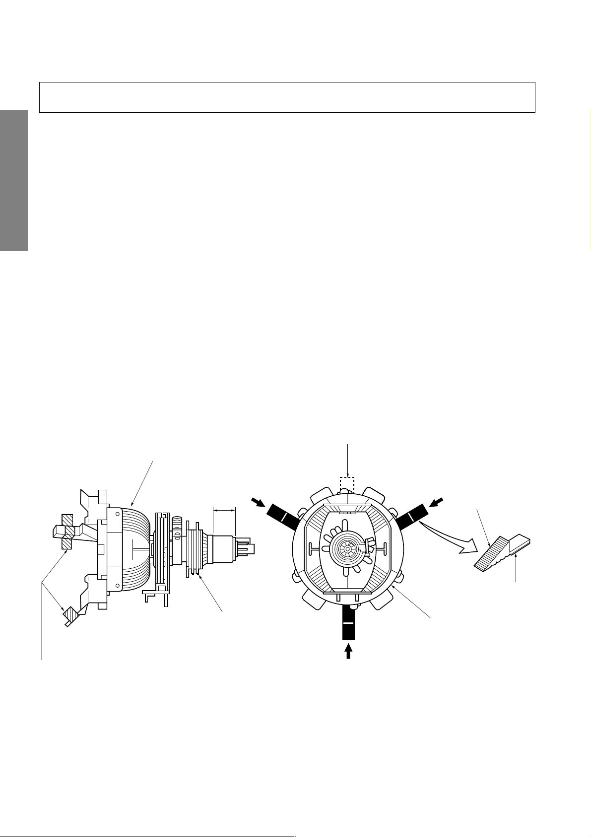
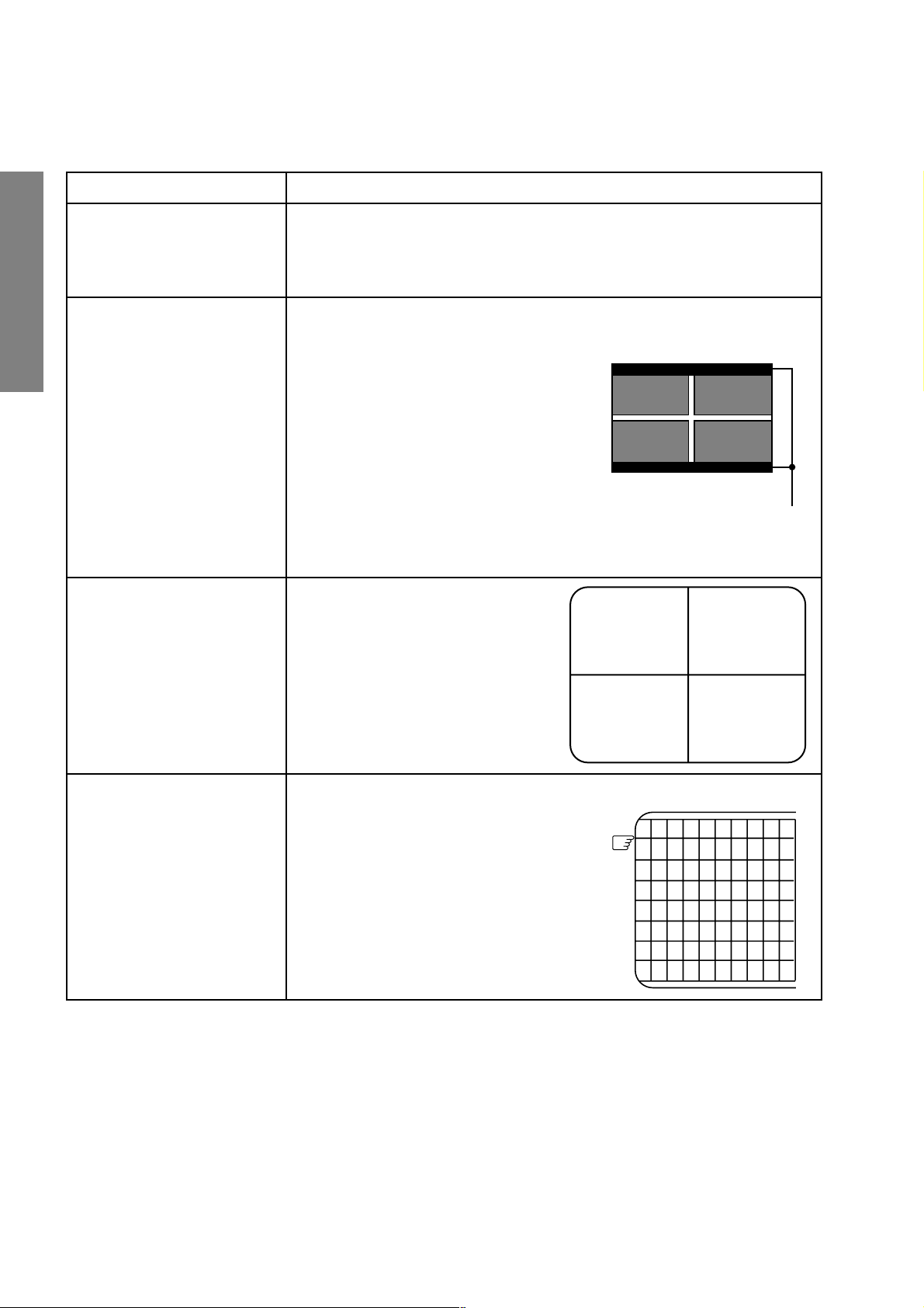
SET-UP ADJUSTMENT
■ The following adjustments should be made when a complete realignment is required or a new picture tube is installed.
Perform the adjustments in order as follows :
1. Color Purity
2. Convergence
3. White Balance
Note: The PURITY/CONVERGENCE MAGNET assembly and rubber wedges need mechanical positioning.
Refer to figure 1.
GENERAL ADJUSTMENTS
*
COLOR PURITY ADJUSTMENT
NOTE : Before attempting any purity adjustments, the receiver
1. Demagnetize the picture tube and cabinet using a degauss-
2. Set the brightness and contrast to maximum.
3. Use a green raster from among the built-in test signals.
4. Loosen the clamp screw holding the yoke and slide the
SPECIFIC INFORMATIONS
Mounting position of the purity magnet assembly should fit to same position as old one because slightly difference to
the position depend on a kind of tube.
There are no adjustment of purity and convergence in some picture tube (Unified with purity magnet)
5. Remove the Rubber Wedges.
should be operated for at least fifteen minutes.
ing coil.
yoke backward or forward to provide vertical green belt
(zone) in the picture screen.
6. Rotate and spread the tabs of the purity magnet (See figure 2.) around the neck of the picture tube until the green
belt is in the center of the screen. At the same time, enter
the raster vertically.
7. Slowly move the yoke forward or backward until a uniform
green screen is obtained. Tighten the clamp screw of the
yoke temporarily.
8. Check the purity of the red and blue raster.
GLASS CLOTH
TAPES
DEFLECTION
YOKE
29.1mm(28", 29")
25mm(25")
19mm(19", 20", 21")
14mm(13", 14")
PURITY/
CONVERGENCE
MAGNET ASS'Y
Figure 1.
TEMPORARY
MOUNTING
RUBBER WEDGE
ADHESIVE
DEFLECTION
YOKE
– 4 –
Page 5
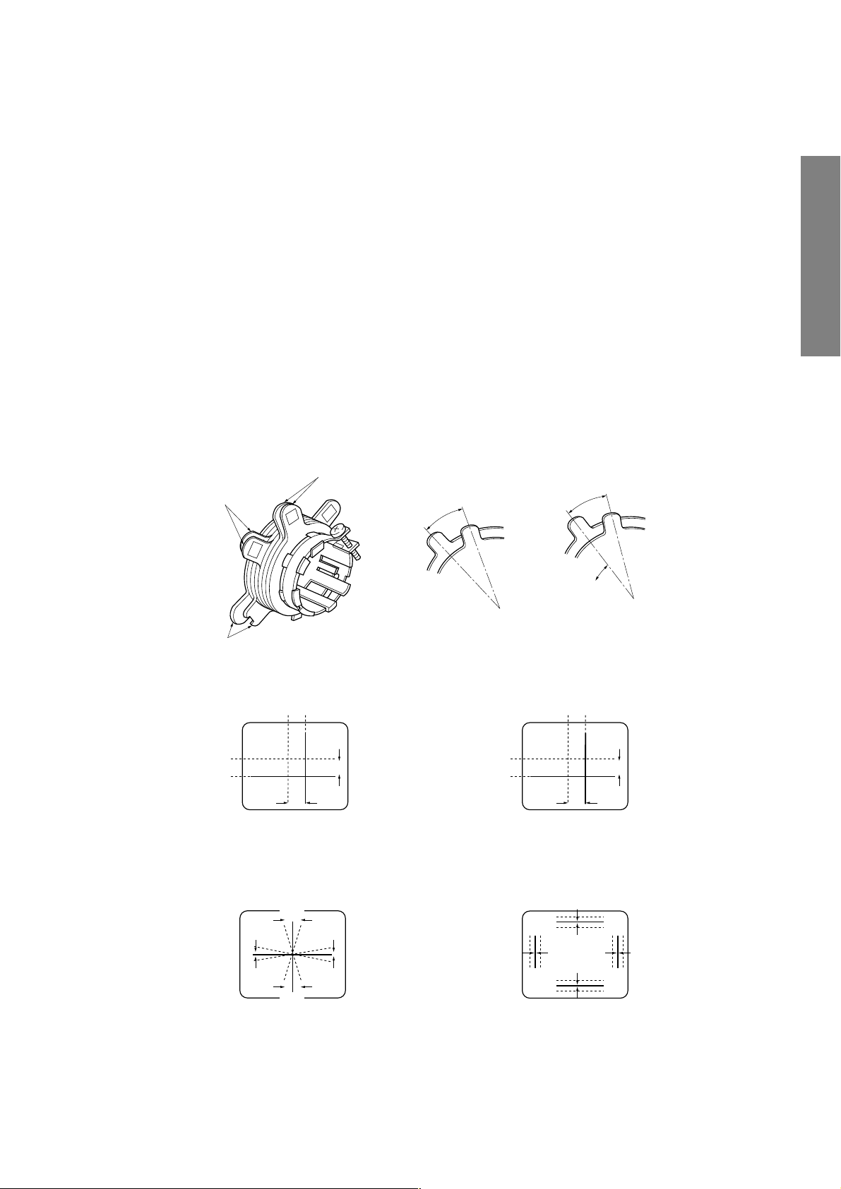
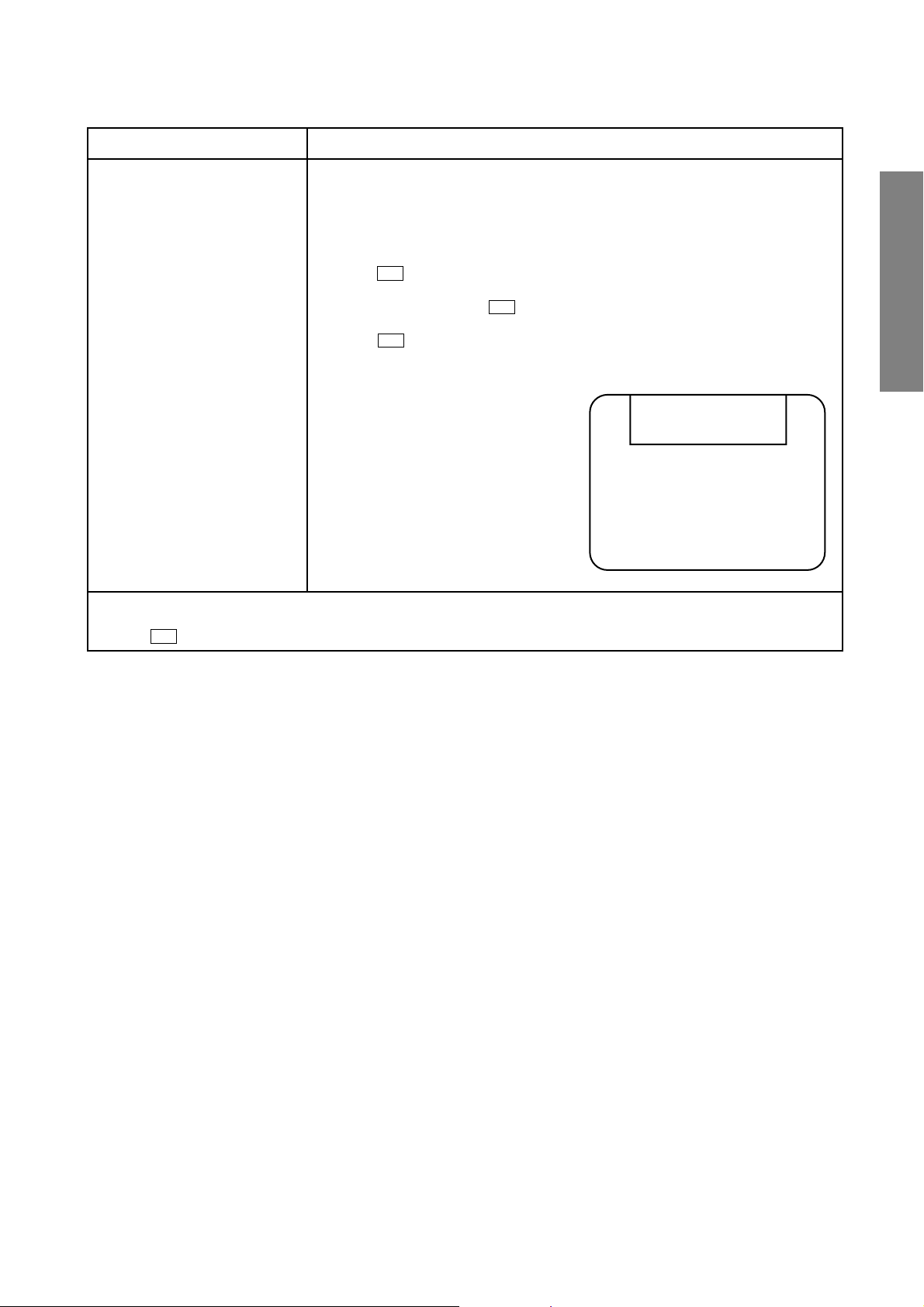
CONVERGENCE ADJUSTMENTS
NOTE: Before attempting any convergence adjustments, the
receiver should be operated for at least fifteen minutes.
■ CENTER CONVERGENCE ADJUSTMENT
1. Use the cross-dot pattern from among the built-in test signals.
2. Set the brightness and contrast for well defined pattern.
3. Adjust two tabs of the 4-Pole Magnets to change the angle between them (See figure 2.) and superimpose red
and blue vertical lines in the center area of the picture
screen.
4. Turn the both tabs at the same time keeping the angle
constant to superimpose red and blue horizontal lines at
the center of the screen.
5. Adjust two tabs of 6-Pole Magnets to superimpose red/
blue line and green one. Adjusting the angle affects the
vertical lines and rotating both magnets affects the horizontal lines.
6. Repeat adjustments 3, 4, 5 keeping in mind red, green
and blue movement, because 4-Pole Magnets and 6-Pole
Magnets have mutual interaction and make dot movement
complex.
6-POLE
4-POLE
MAGNETS
MAGNETS
ADJUST THE ANGLE
(VERTICAL LINES)
■ CIRCUMFERENCE CONVERGENCE ADJUSTMENT
1. Loosen the clamping screw of deflection yoke slightly to
allow the yoke to tilt.
2. Temporarily put a wedge as shown in figure 1. (Do not
remove cover paper on adhesive part of the wedge.)
3. Tilt front of the deflection yoke up or down to obtain better
convergence in circumference. (See figure 3.) Push the
mounted wedge into the space between picture tube and
the yoke to fix the yoke temporarily.
4. Put other wedge into bottom space and remove the cover
paper to stick.
5. Tilt front of the yoke right or left to obtain better convergence in circumference. (See figure 3.)
6. Keep the yoke position and put another wedge in either
upper space. Remove cover paper and stick the wedge
on picture tube to fix the yoke.
7. Detach the temporarily mounted wedge and put it in another upper space. Stick it on picture tube to fix the yoke.
8. After fixing three wedges, recheck overall convergence.
Tighten the screw firmly to fix the yoke and check the yoke
is firm.
9. Stick three adhesive tapes on wedges as shown in figure
1.
FIXED
GENERAL ADJUSTMENTS
ROTATE TWO TABS
AT THE SAME TIME
(HORIZONTAL LINES)
PURITY
MAGNETS
CONVERGENCE MAGNET ASSEMBLY ADJUSTMENT OF MAGNETS
Figure 2.
BLU RED
BLU
RED
4-POLE MAGNETS MOVEMENT
BGR
R
G
B
RGB
RED/BLU
GRN
Center Convergence by Convergence Magnets
B
G
R
RED/BLU GRN
6-POLE MAGNETS MOVEMENT
B
G
R
BGR
RGB
R
G
B
SPECIFIC INFORMATIONS
INCLINE THE YOKE UP (OR DOWN)
Circumference Convergence by DEF Yoke
Figure 3. Dot Movement Pattern
INCLINE THE YOKE RIGHT (OR LEFT)
– 5 –
Page 6
1. ENTERING TO SERVICE MODE
1) Press o button once on
Remote Control.
SERVICE MODE
2) Press o button again to
keep pressing.
3) While pressing the o button,
press MENU button on TV set.
GENERAL ADJUSTMENTS
2. DISPLAYING THE ADJUSTMENT MENU
1) Press MENU button on TV.
Service mode
S
3. KEY FUNCTION IN THE SERVICE MODE
The following key entry during display of adjustment menu provides special functions.
SPECIFIC INFORMATIONS
A single horizontal line ON/OFF: - / - - button (on Remote) or a button (on TV)
Test signal selection : a button (on Remote)
Selection of the adjustment items : Channel s/t (on TV or Remote)
Change of the data value : Volume ; +/– (on TV or Remote)
Adjustment menu mode ON/OFF : MENU button (on TV)
Initialization of the memory (QA02) : CALL + Channel button on TV (s)
Reset the count of operating protect
circuit to “00”: CALL + Channel button on TV (t)
“RCUT” selection : 1 button
“GCUT” selection : 2 button
“BCUT” selection : 3 button
“CNTX” (or “SCNT”) selection : 4 button
“COLC” selection : 5 button
“TNTC” selection : 6 button
Test audio signal ON/OFF (1kHz) : 8 button
Self diagnostic display ON/OFF : 9 button
Press
Press
Adjustment mode
Item
Data
(Service mode display)
Item
Data
S
Color thickness correction
note: Displayed differently as shown below, de-
pending on the setting of the receiving color
system.
COLP (PAL)
COLC (NTSC)
COLS (SECAM)
CAUTION : Never try to perform initialization unless you have changed the memory IC.
– 6 –
Page 7
4. SELECTING THE ADJUSTING ITEMS
1) Every pressing of CHANNEL s button in the service mode changes the adjustment items in the order of table-2.
(t button for reverse order)
Refer to table-2 for preset data of adjustment mode.
(See SETTING & ADJUSTING DATA on page 13)
5. ADJUSTING THE DATA
1) Pressing of VOLUME ; +/– button will change the value of data in the range from 00H to FFH. The variable
range depends on the adjusting item.
6. EXIT FROM SERVICE MODE
1) Pressing POWER button to turn off the TV once.
■ INITIALIZATION OF MEMORY DATA OF QA02
After replacing QA02, the following initialization is required.
1. Enter the service mode, then select any register item.
2. Press and hold the CALL button on the Remote, then press the CHANNEL s button on the TV. The initialization of QA02 has
been complated.
3. Check the picture carefully. If necessary, adjust any adjustment item above.
Perform “Auto search Memory” on the owner’s manual.
CAUTION: Never attempt to initialize the data unless QA02 has been replaced.
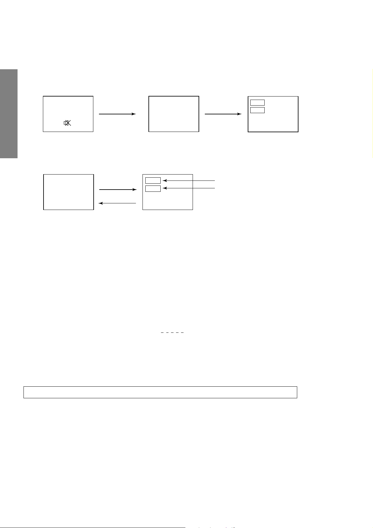
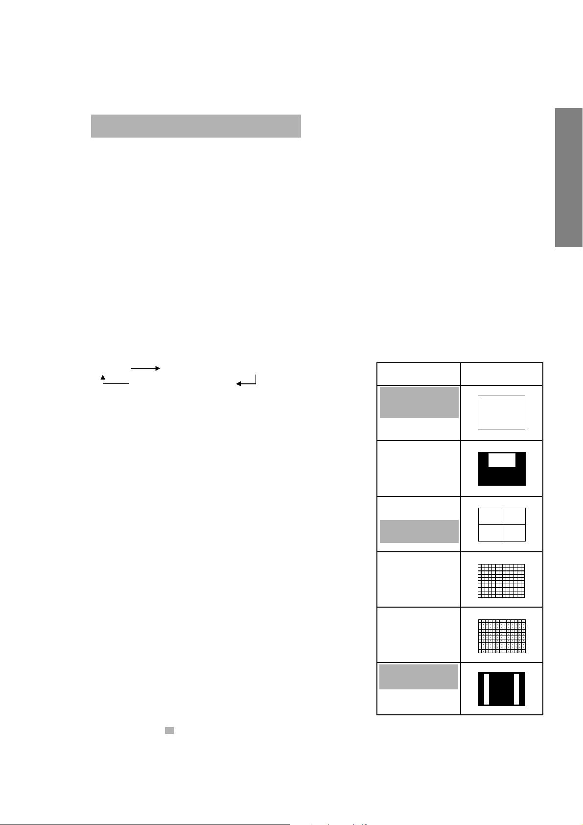
7. TEST SIGNAL SELECTION
1) Every pressing of a button on the Remote Control changes the built-in test patterns on screen as described below
in SERVICE MODE.
GENERAL ADJUSTMENTS
Signal off
NTSC signals (14 patterns)
PAL signals (14 patterns)
Signals Picture
• Red raster
• Green raster
• Blue raster
• All Black
• All White
• Black & White
• Black cross-bar
• White cross-bar
• Black cross-bar
on green raster
• Black cross-hatch
• White cross-hatch
• Black cross-dot
• White cross-dot
SPECIFIC INFORMATIONS
• H signal (white)
• H signal (black)
The signals marked with are not usable to display in the Test signal for some model.
*
– 7 –
Page 8

8. SELF DIAGNOSTIC FUNCTION
1) Press “9” button on Remote Control during display of adjustment menu in the service mode.
The diagnosis will begin to check if interface among IC’s are executed properly.
2) During diagnosis, the following displays are shown.
Indicated color of mode now selected : Green and Red
<SELF CHECK>
23******
POWER : 00
BUS LINE : OK
BUS CONT : OK
BLOCK : UV V1
Indicated color of other modes : White
Green : Normal
Red : The microprocessor operates to provide judgement
of no video signal. The red color is still indicated
though the signal is input, failure may exist in input
signal line.
GENERAL ADJUSTMENTS
Part number of microprocessor (Q100)
Operation number of protecting circuit ----“00” is nor-
mal.
When indication is other than “00”, overcurrent apts to
flow, and circuit parts may possibly be damaged.
BUS LINE CHECK ----“OK” is normal.
“SDA1-GND” ------------- SDA-GND short circuit.
“SCL1-GND” -------------- SCL-GND short circuit.
“SCL1-SDA1” ------------- SCL-SDA short circuit.
BUS CONT ----“OK” is normal.
When indication shows “Q uuu NG”, the device with
SPECIFIC INFORMATIONS
the number may possibly be damaged.
BLOCK
UV : TV reception mode
V1 : VIDEO input mode (a1)
The items marked with are not usable to display in the SELF DIAGNOSTIC FUNCTION for some model.
*
– 8 –
Page 9

1. ENTERING TO DESIGN MODE
1) Select the Service mode.
DESIGN MODE
2) While pressing o (or CALL) button on
Remote and press MENU button on TV.
3) Press MENU button on TV.
S D
(Design mode) (Adjustment mode)
When QA02 is initialized, items “OPT0” and “OPT1” of DESIGN MODE are set to the data of the representative model of this
chassis family.
Therefore, because ON-SCREEN specification remains in the state of the representative of model. This model is required to
reset the data of items “OPT0” and “OPT1”.
2. SELECTING THE ADJUSTING ITEMS
Every pressing of CHANNEL t button in the design mode changes the adjustment items in the order of table-3.
(s button for reverse order)
Refer to table-3 for data of design mode.
(See SETTING & ADJUSTING DATA on page 13)
3. ADJUSTING THE DATA
Pressing of VOLUME s or t button will change the value of data.
Press
Press
ITEM
DATA
GENERAL ADJUSTMENTS
SPECIFIC INFORMATIONS
– 9 –
Page 10
ELECTRICAL ADJUSTMENTS
ITEM ADJUSTMENT PROCEDURE
FOCUS VR ADJ
SUB-BRIGHTNESS
(BRTC)
GENERAL ADJUSTMENTS
SPECIFIC INFORMATIONS
Note: Constrict the picture height
until the vertical retrace line
appears adjusting the item
HIT (HEIGHT).
HORIZONTAL POSITION
ADJUSTMENT (HPOS)
VERTICAL POSITION
ADJUSTMENT (VPOS)
1. Enter the service mode, then select any register item.
2. Press the TV/VIDEO button on the Remote until the black cross-bar pattern appears on the screen.
3. Adjust the FOCUS control (on T461) for well defined scanning lines on the picture
screen.
1. Set CONTRAST to minimum, and
BRIGHTNESS to center by adjusting
user controls.
2. Set the TV in service mode to get white
cross-bar of inside pattern.
3. Select BRTC (brightness correction),
and adjust the ; – /+ button to reduce
the value so that white portion of inside
pattern slightly light.
4. Adjust ; – /+ button to increase the
data value of BRTC, and set it just
before the difference between the belt of
vertical retrace and the border of black
portion of inside pattern is visible.
After that, return vertical height and
contrast.
1. Set the TV in service mode, and get
black or white cross-bar signal with
VIDEO button on remote hand unit.
2. Select either HPOS (Horizontal
picture phase) or VPOS (Vertical
picture phase) with CHANNEL s, t
buttons, and adjust horizontal or
vertical picture position in the center
of screen with VOLUME ; – /+
buttons.
Belt of vertical retrace
VERTICAL AMPLITUDE
ADJUSTMENT (HIT)
1. Set the TV in service mode, and get
black or white cross-hatch signal
with VIDEO button on remote hand
unit.
2. Select HIT (Vertical amplitude) with
CHANNEL s, t buttons, and adjust
vertical amplitude with VOLUME
; – /+ buttons so that vertical amplitude lacks a little.
3. Adjust vertical amplitude with VOLUME ; – /+ buttons so that the first
bar on cross-hatch signal touches
edge of screen.
The first
– 10 –
Page 11
ITEM ADJUSTMENT PROCEDURE
WHITE BALANCE
ADJUSTMENT
CUTOFF ADJUSTMENT
•
(RCUT)
(GCUT)
(BCUT)
DRIVE ADJUSTMENT
•
(GDRV)
(BDRV)
NOTE: It is released built-in test pattern by changing the adjustment item for some model.
In this case, select the adjustment item with channel s t buttons first and then select the built-in test pattern with
-/- - button.
1. Set Contrast to 40, and brightness to +20 by picture control.
2. Set the TV in service mode, and get the inside W/B adjusting signal with VIDEO
button.
3. Select RCUT, GCUT and BCUT with CHANNEL s, t buttons, to set individual
values to Initial reference data, and to set GDRV and BDRV to Initial reference
data with VOLUME ; – /+ buttons.
4. Press -/- - button on the remote control and rotate Screen VR to get one slight
horizontal line on screen.
Note: Every pressing of -/- - button provides Horizontal line picture and Normal
picture alternately.
5. Press -/- - button to release horizontal line picture, and select the two other colors
which did not light in the above step with CHANNEL s, t buttons. Then tap VOLUME ; – /+ buttons so that three colors slightly light in the same level.
X To correct white balance in light area,
select GDRV and BDRV with CHANNEL
s, t buttons to adjust.
X To correct white balance in dark area,
perform fine adjustment of RCUT, GCUT
and BCUT.
GENERAL ADJUSTMENTS
Light area check
(to show white)
Dark area check
(to show black)
SPECIFIC INFORMATIONS
– 11 –
Page 12

CIRCUIT CHECK
HIGH VOLTAGE CHECK
CAUTION: There is no HIGH VOLTAGE ADJUSTMENT on this chassis. Checking should be done following the steps
below.
1. Connect an accurate high voltage meter to the second anode of the picture tube.
2. Turn on the receiver. Set the BRIGHTNESS and CONTRAST controls to minimum (zero beam current).
3. High voltage must be measured below (B) kV.
Refer to table-1 for high voltage (B).
(See SETTING & ADJUSTING DATA on page 13)
4. Vary the BRIGHTNESS control to both extremes to be sure the high voltage does not exceed the limit under any conditions.
GENERAL ADJUSTMENTS
SPECIFIC INFORMATIONS
– 12 –
Page 13
CHAPTER 2 SPECIFIC INFORMATIONS
SETTING & ADJUSTING DATA
SAFETY INSTRUCTIONS
HIGH VOLTAGE AT ZERO BEAM: (A) 23.5 kV
MAX HIGH VOLTAGE:
AC VOLTAGE
Table-1
SERVICE MODE
ADJUSTING ITEMS AND DATAS IN THE SERVICE MODE:
14"
(B) 25.0 kV
(C) 110~240 V
Item Adjustment Reference data
RCUT
GCUT
BCUT
GDRV
BDRV
BRTC
COLC
TNTC
COLP
COLS
SCNT
HPOS
VPOS
HIT
VLIN
SRY
SBY
RAGC
R CUT OFF
G CUT OFF
B CUT OFF
G DRIVE
B DRIVE
BRIGHTNESS CENTER
COLOR CENTER NTSC
TINT CENTER
COLOR CENTER PAL (difference from COLC)
COLOR CENTER SECAM
SUB CONTRAST
HORIZONTAL POSITION
VERTICAL POSITION 50Hz
HEIGHT 50Hz
VERT. LINEARITY 50Hz
SECAM R-Y BLACK ADJUST
SECAM B-Y BLACK ADJUST
RF AGC
Table-2
0DH
1EH
0AH
2AH
20H
20H
20H
40H
40H
40H
30H
45H
09H
30H
08H
04H
08H
08H
Data
←
←
←
←
←
←
←
←
←
←
←
←
←
←
←
←
←
←
SPECIFIC INFORMATIONS
DESIGN MODE
ADJUSTING ITEMS AND DATAS IN THE DESIGN MODE:
Item Name of adjustment
OPT
OPT1
OPTIONAL SETTING
OPTIONAL SETTING 1
– 13 –
Data
Preset Data 14"
75H
15H
Table-3
←
05H
Remarks
Page 14
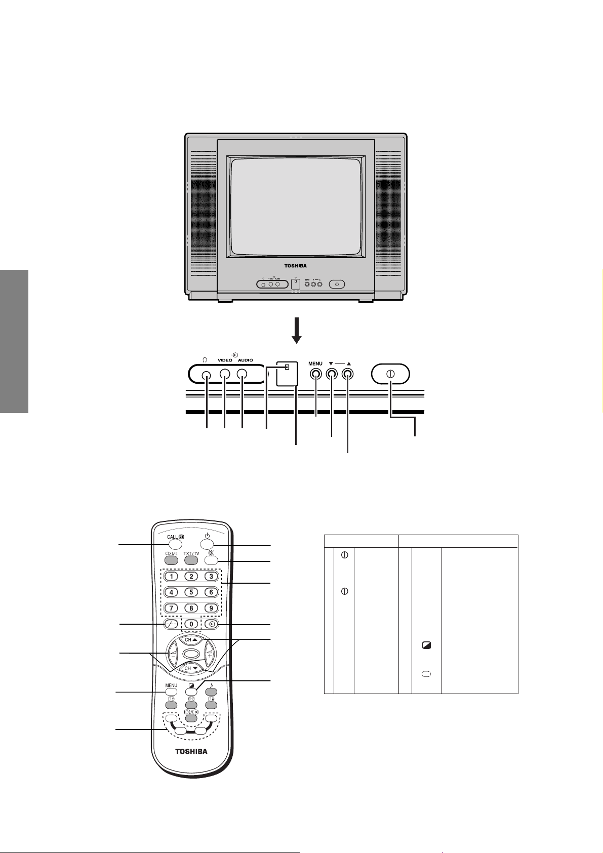
LOCATION OF CONTROLS (Representative: 21S1MJ)
Front
SPECIFIC INFORMATIONS
Remote
0
5
4
6
-
i
h
g
c
1
7
2
9
3
8
b
d
f
a
e
Names of Parts
TV Set
a Main power
b Infrared
c
d
e s Channel up
f t Channel
g
h
i
MENU
AUDIO
VIDEO
l
on/off
sensor
Power
indicator
Menu open
down
Audio input
terminal
Video input
terminal
Headphone
jack
Note: The shaded buttons are not available
for your TV. If you press the button,
”MODE NOT AVAILABLE” will appear on
the screen.
Remote Controller
1 f Power on/standby
2 0~9 Direct select
3 CHs/t Channel up/down,
4 ; -/+ Volume up/down,
5 -/-- Digit select
6
7 o Sound mute
8
9 a TV/VIDEO select
0 CALL On-screen on/off
-
Item select
Menu select, Level adjust
MENU
Menu open
Picture control
Game select
RGYB
Red/Green/Yellow/Blue
– 14 –
Page 15

CHANNEL PRESET
Use this function when:
• You cannot find the channel you want
using “Selecting the channel” on page 9.
• The color or sound is strange.
Technical Term
Channel: The number or abbreviation of
the broadcast station frequency
in each country (Channel 5,
Channel 8, Arts Central, Channel U
etc.)
Position: The number on your TV given
to stored channels (0~199). It is
displayed on the upper right of
the screen.
Auto search memory (ASM)
All the channels that can be received are
preset automatically.
1 Select the starting position for ASM. Press
(0~9) or CHs/t.
2 Set the correct broadcast system for your
region. Press MENU and ;
“SET UP” menu
“AUTO” and set “SOUND” according to the
table above using CHs/t and ;
3 Press MENU and ;
“TUNING” menu
press ;
screen returns to the start position, the
procedure is complete.
+ to start the search. When the TV
D7
D8
–/+ to call up the
. Set “COLOR” to
–/+.
–/+ to call up the
. Select “ASM”, then
2 Press MENU and ; –/+ to call up the
“TUNING” menu
select “ SEARCH” . Press ;
search. Pressing “-” searches for channels
at lower frequencies while pressing
“+” searches for channels at higher
frequencies.
3 When Channel 12 is found, press CH
select “MEMORY”. Press “+” to complete
the presetting.
Method 2 - Store Position
1 Select Channel 12.
Press (0~9) or CH
preset for Channel 12.
2 When Channel 12 is selected, press
MENU and ;
menu
“POSITION”. Press ;
“POSITION” to P012. Pressing “-” and “+”
respectively decreases and increases
the position number.
3 When Position 12 is found, press CH
to select “MEMORY”. Press “+” to complete
the presetting.
D8
–/+ to call up the “TUNING”
. Press CH s / t and select
. Press CH s/t and
D8
–/+ to
s/t to
s/t to find the position
–/+ and set
s/t
Skip Function
If you set “SKIP ON” for unnecessary
position numbers, these will be skipped
when selecting channels using CH
s/t.
SPECIFIC INFORMATIONS
Manual Search and Changing the
assigned position
For easy Channel selection, the chosen
Position should have the same number as
Channel stored there. For this operation, you
may use the “SEARCH” and “SKIP” functions.
Example : Presetting Channel 12 to Position 12
Method 1 - Manual Search
1 Select Position 12.
Press CH
Or, press -/-- twice to display “--” on the
screen then press the “1” and “2” buttons
in this order.
s/t repeatedly until 12 is displayed.
Example : Skipping Channel 13
1 Select Position 13 using the same method
for selecting Position 12 (above).
2 Press MENU and ;
“SET UP” menu
select “ SKIP”. Press ;
the “SKIP” setting from “OFF” to “ON”.
This completes the setting for skipping
Position 13.
–/+ to call up the
. Press CHs/t and
D7
–/+ to switch
– 15 –
Page 16

Note:
• When “SKIP” is ON, the Position number is
prefixed by “*”.
Example: *13. To confirm this, select Position
13 using the -/-- and 0~9 buttons.
• If you want to restore a skipped position
number, select it using the -/-- and 0~9
buttons then switch the “SKIP” setting to
“OFF” as in step 2 above.
Manual fine tuning (MFT)
Under some reception conditions, fine
tuning may be necessary to improve the
picture quality. In such cases, adjust the
manual fine tuning (MFT).
1 Press MENU and ;
“TUNING” menu
2 Press CH
to start fine tuning. Pressing “-” fine tunes
to a lower frequency while pressing “+”
fine tunes to a higher frequency.
s/t and select “MFT”. Press ; –/+
D8
–/+ to call up the
.
Auto fine tuning (AFT)
If the signal frequency is unstable due
SPECIFIC INFORMATIONS
to environmental conditions, use auto
fine tuning.
1 Press MENU and ;
“TUNING” menu
2 Press CHs/t and select “AFT”. Press ;
to switch it to “ON”. This completes the
setting.
Notes:
• When you operate MFT, AFT is switched
OFF automatically. If you switch on AFT
after fine tuning with MFT, MFT may be
cancelled.
• AFT may be set independently for each
Position.
D8
–/+ to call up the
.
–/+
– 16 –
Page 17

CHASSIS AND CABINET REPLACEMENT PARTS LIST
WARNING: BEFORE SERVICING THIS CHASSIS, READ THE "X-RAY RADIATION PRECAUTION", "SAFETY PRE-
CAUTION" AND "PRODUCT SAFETY NOTICE" ON PAGE 3 OF THIS MANUAL.
CAUTION: The international hazard symbols " " in the schematic diagram and the parts list designate components
which have special characteristics important for safety and should be replaced only with types identical to those in the
original circuit or specified in the parts list. The mounting position of replacements is to be identical with originals.
Before replacing any of these components, read carefully the PRODUCT SAFETY NOTICE. Do not degrade the safety
of the receiver through improper servicing.
NOTICE:
··
·
The part number must be used when ordering parts, in order to assist in processing, be sure to include the
··
Model number and Description.
··
·
The PC board assembly with * mark is no longer available after the end of the production.
··
Model : 14SV2M
Capacitors ............. CD : Ceramic Disk PF : Plastic Film EL : Electrolytic
Resistors ............... CF : Carbon Film CC : Carbon Composition MF : Metal Film
OMF : Oxide Metal Film VR : Variable Resistor FR : Fusible Resistor
(All CD and PF capacitors are
±5%, 50V and all resistors, ±5%, 1/6W unless otherwise noted.)
Location Parts No. Description
No.
CAPACITORS
C102 24763221 ELECTROLYTIC, 16V 220UF M
C106 24796479 ELECTROLYTIC, 35V 4.7UF M
C108 24503049 PLASTIC FILM, 63V 0.47UF J
C113 24109102 CERAMIC CHIP, 50V B 1000PF K
C114 24109102 CERAMIC CHIP, 50V B 1000PF K
C118 24109102 CERAMIC CHIP, 50V B 1000PF K
C120 24203100 ELECTORLYTIC, 16V 10UF M 7L 3A
C121 24109103 CERAMIC CHIP, 50V B 0.01UF K
C123 24206010 ELECTROLYTIC, 50V 1.0UF M 7L 3A
C129 24109102 CERAMIC CHIP, 50V B 1000PF K
C130 24206479 ELECTROLYTIC, 50V 4.7UF M 7L 3A
C131 24814103 CERAMIC CHIP, 50V F 0.01UF Z
C132 24100104 CERAMIC CHIP, 25V F 0.1UF Z
C133 24105101 CERAMIC CHIP, 50V CH 100PF J
C135 24109222 CERAMIC CHIP, 50V B 2200PF K
C136 24206228 ELECTROLYTIC, 50V 0.22UF M 7L 3A CE04WS
C137 24100103 CERAMIC CHIP, 50V F 0.01UF Z
C141 24105101 CERAMIC CHIP, 50V CH 100PF J
C150 24814103 CERAMIC CHIP, 50V F 0.01UF Z
C166 24109103 CERAMIC CHIP, 50V B 0.01UF K
C167 24763101 ELECTROLYTIC, 16V 100UF M
C170 24109103 CERAMIC CHIP, 50V B 0.01UF K
C171 24203100 ELECTORLYTIC, 16V 10UF M 7L 3A
C172 24203100 ELECTORLYTIC, 16V 10UF M 7L 3A
C173 24203100 ELECTORLYTIC, 16V 10UF M 7L 3A
C174 24105330 CERAMIC CHIP, 50V CH 33PF J
C175 24105330 CERAMIC CHIP, 50V CH 33PF J
C176 24105330 CERAMIC CHIP, 50V CH 33PF J
C189 24206478 ELECTROLYTIC, 50V 0.47UF M 7L 3A
C192 24206478 ELECTROLYTIC, 50V 0.47UF M 7L 3A
C216 24206010 ELECTROLYTIC, 50V 1.0UF M 7L 3A
C221 24105101 CERAMIC CHIP, 50V CH 100PF J
C222 24105101 CERAMIC CHIP, 50V CH 100PF J
C223 24105101 CERAMIC CHIP, 50V CH 100PF J
C224 24203100 ELECTORLYTIC, 16V 10UF M 7L 3A
C226 24591104 PLASTIC FILM, 50V 0.1UF J
C227 24591104 PLASTIC FILM, 50V 0.1UF J
C231 24232103 CERAMIC DISC, 50V F 0.01UF Z
C232 24232103 CERAMIC DISC, 50V F 0.01UF Z
C305 24617915 ELECTROLYTIC, 50V 1UF K 3A LI
C306 24763102 ELECTROLYTIC, 16V 1000UF M
C307 24693473 PLASTIC FILM, 100V 0.047UF J
C308 24765101 ELECTROLYITC, 35V 100UF M
C312 24765102 ELECTROLYTIC CE04G 35V 1000UF M
C313 24082280 PLASTIC FILM, 100V 0.22UF J
Location Parts No. Description
No.
C314 24212152 CERAMIC DISC, 50V B 1500PF K
C317 24214471 CERAMIC DISC, 500V B 470PF K
C320 24765101 ELECTROLYITC, 35V 100UF M
C399 24503049 PLASTIC FILM, 63V 0.47UF J
C410 24693472 PLASTIC FILM, 100V 4700PF J
C417 24214102 CERAMIC DISC, 500V B 1000PF K
C420 24203220 ELECTROLYTIC, 16V 22UF M 7L 3A
C421 24763470 16MV47HC +T 16MV47HC +T
C431 24206479 ELECTROLYTIC, 50V 4.7UF M 7L 3A
C432 24203100 ELECTORLYTIC, 16V 10UF M 7L 3A
C433 24100103 CERAMIC CHIP, 50V F 0.01UF Z
C434 24100103 CERAMIC CHIP, 50V F 0.01UF Z
C435 24763102 ELECTROLYTIC, 16V 1000UF M
C436 24206478 ELECTROLYTIC, 50V 0.47UF M 7L 3A
C437 24109822 CERAMIC CHIP, 50V B 8200PF K
C440 24503264 PLASTIC FILM CF92 T 1250VH 7200PF H
C442 24082969 PLASTIC FILM, 250V 0.39UF J
C445 24693104 PLASTIC FILM, 100V 0.1UF J
C446 24679100 ELECTROLYTIC, 250V 10UF M 3A
C448 24073118 ELECTROLYTIC, 160V 33UF M
C449 24794471 ELECTROLYTIC, 16V 470UF M
C463 24109152 CERAMIC CHIP, 50V B 1500PF K
C484 24591104 PLASTIC FILM, 50V 0.1UF J
C485 24591104 PLASTIC FILM, 50V 0.1UF J
C502 24591103 PLASTIC FILM, 50V 0.01UF J
C517 24203100 ELECTORLYTIC, 16V 10UF M 7L 3A
C523 24203100 ELECTORLYTIC, 16V 10UF M 7L 3A
C526 24109102 CERAMIC CHIP, 50V B 1000PF K
C528 24206478 ELECTROLYTIC, 50V 0.47UF M 7L 3A
C567 24109103 CERAMIC CHIP, 50V B 0.01UF K
C610 24795100 ELECTROLYTIC, 25V 10UF M
C612 24797220 ELECTROLYTIC, 50V 22UF M
C613 24591104 PLASTIC FILM, 50V 0.1UF J
C615 24763101 ELECTROLYTIC, 16V 100UF M
C631 24206478 ELECTROLYTIC, 50V 0.47UF M 7L 3A
C632 24591682 PLASTIC FILM, 50V 6800PF J
C633 24591393 PLASTIC FILM, 50V 0.039UF J
C634 24591103 PLASTIC FILM, 50V 0.01UF J
C660 24206478 ELECTROLYTIC, 50V 0.47UF M 7L 3A
C661 24591104 PLASTIC FILM, 50V 0.1UF J
C665 24073060 ELECTROLYTIC, 25V 4700UF M 3A
C667 24591104 PLASTIC FILM, 50V 0.1UF J
C668 24764471 ELECTROLYTIC, 25V 470UF M
C669 24766100 ELECTROLYTIC, 50V 10UF M
C801 24503507 PLASTIC FILM, AC275V 0.22UF K
C805 24092281 CERAMIC DISC, AC250V E 4700PF
SPECIFIC INFORMATIONS
– 17 –
Page 18

Location Parts No. Description
No.
C806 24092281 CERAMIC DISC, AC250V E 4700PF
C810 24086059 ELECTROLYTIC, 400V 270UF M 3D
C813 24092555 CERAMIC DISC, AC250V E 1000PF M
C814 24092555 CERAMIC DISC, AC250V E 1000PF M
C861 24214471 CERAMIC DISC, 500V B 470PF K
C864 24797221 ELECTROLYTIC, 50V 220UF M
C873 24092341 CERAMIC DISC, 2KV R 470PF K
C874 24591104 PLASTIC FILM, 50V 0.1UF J
C875 24109681 CERAMIC CHIP, 50V B 680PF K
C876 24109102 CERAMIC CHIP, 50V B 1000PF K
C877 24100103 CERAMIC CHIP, 50V F 0.01UF Z
C878 24092341 CERAMIC DISC, 2KV R 470PF K
C879 24206479 ELECTROLYTIC, 50V 4.7UF M 7L 3A
C880 24100103 CERAMIC CHIP, 50V F 0.01UF Z
C884 24640018 ELECTROLYTIC, 160V 220UF
C885 24214471 CERAMIC DISC, 500V B 470PF K
C886 24214471 CERAMIC DISC, 500V B 470PF K
C887 24764471 ELECTROLYTIC, 25V 470UF M
C889 24764102 ELECTROLYTIC 04G, 25V 1000UF M
C893 24092341 CERAMIC DISC, 2KV R 470PF K
C896 24092553 CERAMIC DISC, AC250V B 470PF K
C897 24092557 CERAMIC DISC, AC250V E 2200PF M
C899 24503045 PLASTIC FILM, 63V 0.22UF J
C902 24092345 CERAMIC DISC, 2KV 1000PF K
C904 24109391 CERAMIC CHIP CK73B 50V 390PF K
C905 24109331 CERAMIC CHIP, 50V B 330PF K
C907 24109391 CERAMIC CHIP CK73B 50V 390PF K
C910 24766478 ELECTROLYTIC, 50V 0.47UF M
C912 24763471 ELECTROLYTIC, 16V 470UF M
C913 24203100 ELECTORLYTIC, 16V 10UF M 7L 3A
C971 24203470 ELECTROLYTIC, 16V 47UF M 7L 3A
CA01 24232103 CERAMIC DISC, 50V F 0.01UF Z
CA02 24105101 CERAMIC CHIP, 50V CH 100PF J
CA03 24105220 CERAMIC CHIP, 50V CH 22PF J
SPECIFIC INFORMATIONS
CA04 24105220 CERAMIC CHIP, 50V CH 22PF J
CA30 24105270 CERAMIC CHIP, 50V CH 27PF J
CA42 24203100 ELECTORLYTIC, 16V 10UF M 7L 3A
CA45 24109103 CERAMIC CHIP, 50V B 0.01UF K
CA51 24109272 CERAMIC CHIP, 50V B 2700PF K
CA52 24109152 CERAMIC CHIP, 50V B 1500PF K
CA53 24105181 CERAMIC CHIP, 50V CH 180PF J
CA54 24766330 ELECTROLYTIC, 50V 33UF M
CA55 24206010 ELECTROLYTIC, 50V 1.0UF M 7L 3A
CA58 24105101 CERAMIC CHIP, 50V CH 100PF J
CA60 24206479 ELECTROLYTIC, 50V 4.7UF M 7L 3A
CB01 24203470 ELECTROLYTIC, 16V 47UF M 7L 3A
CC01 24109103 CERAMIC CHIP, 50V B 0.01UF K
CS01 24203220 ELECTROLYTIC, 16V 22UF M 7L 3A
CS02 24203100 ELECTORLYTIC, 16V 10UF M 7L 3A
CV10 24762471 ELECTROLYTIC, 10V 470UF M
CV11 24203220 ELECTROLYTIC, 16V 22UF M 7L 3A
RESISTORS
R101 24011563 CHIP, METAL FILM, 1/20W 56K OHM J
R102 24011123 CHIP, METAL FILM, 1/20W 12K OHM J
R105 24011121 CHIP, METAL FILM, 1/20W 120 OHM J
R106 24011332 CHIP, METAL FILM, 1/20W 3.3K OHM J
R108 24011122 CHIP, METAL FILM, 1/20W 1.2K OHM J
R109 24011682 CHIP, METAL FILM, 1/20W 6.8K OHM J
R110 24011681 CHIP, METAL FILM, 1/20W 680 OHM J
R111 24011330 CHIP, 1/20W 33 OHM J
R112 24011221 CHIP, METAL FILM, 1/20W 220 OHM J
R113 24011222 CHIP, METAL FILM, 1/20W 2.2K OHM J
R114 24011472 CHIP, METAL FILM, 1/20W 4.7K OHM J
R116 24011682 CHIP, METAL FILM, 1/20W 6.8K OHM J
R117 24011222 CHIP, METAL FILM, 1/20W 2.2K OHM J
R118 24011821 CHIP, METAL FILM, 1/20W 820 OHM J
R120 24011684 CHIP, METAL FILM, 1/20W 680K OHM J
R121 24011221 CHIP, METAL FILM, 1/20W 220 OHM J
R122 24000445 CHIP JUMPER, 1608TYPE
R130 24011101 CHIP, METAL FILM, 1/20W 100 OHM J
R131 24011221 CHIP, METAL FILM, 1/20W 220 OHM J
R132 24011271 CHIP, METAL FILM, 1/20W 270 OHM J
R133 24011271 CHIP, METAL FILM, 1/20W 270 OHM J
R134 24011561 CHIP, METAL FILM, 1/20W 560 OHM J
R135 24011103 CHIP, METAL FILM, 1/20W 10K OHM J
Location Parts No. Description
No.
R136 24011513 CHIP, METAL FILM, 1/20W 51K OHM J
R139 24011332 CHIP, METAL FILM, 1/20W 3.3K OHM J
R140 24011101 CHIP, METAL FILM, 1/20W 100 OHM J
R141 24011331 CHIP, METAL FILM, 1/20W 330 OHM J
R142 24011102 CHIP, METAL FILM, 1/20W 1K OHM J
R143 24011333 CHIP, METAL FILM, 1/20W 33K OHM J
R144 24011103 CHIP, METAL FILM, 1/20W 10K OHM J
R145 24011303 CHIP, METAL FILM, 1/20W 30K OHM J
R146 24011224 CHIP, METAL FILM, 1/20W 220K OHM J
R147 24011152 CHIP, METAL FILM, 1/20W 1.5K OHM J
R148 24011222 CHIP, METAL FILM, 1/20W 2.2K OHM J
R150 24000445 CHIP JUMPER, 1608TYPE
R156 24553153 OXIDE METAL FILM, 1W 15K OHM J
R158 24011122 CHIP, METAL FILM, 1/20W 1.2K OHM J
R166 24011103 CHIP, METAL FILM, 1/20W 10K OHM J
R167 24011103 CHIP, METAL FILM, 1/20W 10K OHM J
R168 24011473 CHIP, METAL FILM, 1/20W 47K OHM J
R169 24011102 CHIP, METAL FILM, 1/20W 1K OHM J
R171 24011473 CHIP, METAL FILM, 1/20W 47K OHM J
R172 24011162 CHIP, METAL FILM, 1/20W 1.6K OHM J
R173 24011102 CHIP, METAL FILM, 1/20W 1K OHM J
R174 24011473 CHIP, METAL FILM, 1/20W 47K OHM J
R175 24011223 CHIP, METAL FILM, 1/20W 22K OHM J
R176 24011473 CHIP, METAL FILM, 1/20W 47K OHM J
R177 24011223 CHIP, METAL FILM, 1/20W 22K OHM J
R178 24011103 CHIP, METAL FILM, 1/20W 10K OHM J
R179 24011222 CHIP, METAL FILM, 1/20W 2.2K OHM J
R180 24011473 CHIP, METAL FILM, 1/20W 47K OHM J
R181 24011223 CHIP, METAL FILM, 1/20W 22K OHM J
R182 24011162 CHIP, METAL FILM, 1/20W 1.6K OHM J
R190 24011101 CHIP, METAL FILM, 1/20W 100 OHM J
R191 24011330 CHIP, 1/20W 33 OHM J
R192 24011330 CHIP, 1/20W 33 OHM J
R194 24011102 CHIP, METAL FILM, 1/20W 1K OHM J
R196 24011102 CHIP, METAL FILM, 1/20W 1K OHM J
R217 24011104 CHIP, METAL FILM, 1/20W 100K OHM J
R227 24366303 CARBON FILM, 1/6W 30K OHM J
R228 24011271 CHIP, METAL FILM, 1/20W 270 OHM J
R229 24011271 CHIP, METAL FILM, 1/20W 270 OHM J
R230 24011271 CHIP, METAL FILM, 1/20W 270 OHM J
R301 24366163 CARBON FILM, 1/6W 16K OHM J
R305 24323159 OXIDE METAL FILM, 2W 1.5 OHM J
R306 24366563 CARBON FILM, 1/6W 56K OHM J
R307 24366103 CARBON FILM, 1/6W 10K OHM J
R312 24552272 OXIDE METAL FILM, 1/2W 2.7K OHM J
R313 24366513 CARBON FILM, 1/6W 51K OHM J
R316 24011392 CHIP, METAL FILM, 1/20W 3.9K OHM J
R317 24011392 CHIP, METAL FILM, 1/20W 3.9K OHM J
R333 24531120 FUSIBLE, 1/2W 12 OHM J
R336 24383331 OXIDE METAL FILM, 2W 330 OHM J
R410 24011181 CHIP, METAL FILM, 1/20W 180 OHM J
R411 24011561 CHIP, METAL FILM, 1/20W 560 OHM J
R416 24019323 OXIDE METAL FILM, 5W 1.8K OHM J
R421 24011391 CHIP, METAL FILM, 1/20W 390 OHM J
R430 24366103 CARBON FILM, 1/6W 10K OHM J
R431 24531120 FUSIBLE, 1/2W 12 OHM J
R433 24011182 CHIP, METAL FILM, 1/20W 1.8K OHM J
R434 24552271 OXIDE METAL FILM, 1/2W 270 OHM J
R435 24011822 CHIP, METAL FILM, 1/20W 8.2K OHM J
R437 24366682 CARBON FILM, 1/6W 6.8K OHM J
R442 24383331 OXIDE METAL FILM, 2W 330 OHM J
R447 24553472 OXIDE METAL FILM, 1W 4.7K OHM J
R448 24321228 OXIDE METAL FILM, 1/2W 0.22 OHM J
R479 24011101 CHIP, METAL FILM, 1/20W 100 OHM J
R491 24011103 CHIP, METAL FILM, 1/20W 10K OHM J
R499 24366202 CARBON FILM, 1/6W 2K OHM J
R603 24011393 CHIP, METAL FILM, 1/20W 39K OHM J
R607 24011101 CHIP, METAL FILM, 1/20W 100 OHM J
R611 24011104 CHIP, METAL FILM, 1/20W 100K OHM J
R612 24011103 CHIP, METAL FILM, 1/20W 10K OHM J
R622 24000445 CHIP JUMPER, 1608TYPE
R630 24011123 CHIP, METAL FILM, 1/20W 12K OHM J
R631 24011822 CHIP, METAL FILM, 1/20W 8.2K OHM J
R632 24011472 CHIP, METAL FILM, 1/20W 4.7K OHM J
R662 24552221 OXIDE METAL FILM, 1/2W 220 OHM J
R663 24552221 OXIDE METAL FILM, 1/2W 220 OHM J
– 18 –
Page 19

Location Parts No. Description
No.
R664 24366339 CARBON FILM, 1/6W 3.3 OHM J
R665 24011224 CHIP, METAL FILM, 1/20W 220K OHM J
R801 24009954 METAL FILN, 1/2W 2.2M OHM J
R808 24019476 THERMISTOR, POSITIVE, AC290V 18 OHM M
R810 24568229 CERAMIC COVERED, 7W 2.2 OHM J
R814 24383123 OXIDE METAL FILM, 2W 12K J
R815 24383123 OXIDE METAL FILM, 2W 12K J
R816 24366471 CARBON FILM, 1/6W 470 OHM J
R817 24366331 CARBON FILM, 1/6W 330 OHM J
R840 24366362 CARBON FILM, 1/6W 3.6K OHM J
R860 24383104 OXIDE METAL FILM, 2W 100K OHM J
R861 24011683 CHIP, METAL FILM, 1/20W 68K OHM J
R864 24310479 OXIDE METAL FILM, 1/2W 4.7 OHM J
R873 24011562 CHIP, METAL FILM, 1/20W 5.6K OHM J
R874 24322398 OXIDE METAL FILM, 1W 0.39 OHM J
R875 24322398 OXIDE METAL FILM, 1W 0.39 OHM J
R876 24011221 CHIP, METAL FILM, 1/20W 220 OHM J
R877 24011103 CHIP, METAL FILM, 1/20W 10K OHM J
R878 24366824 CARBON FILM, 1/6W 820K OHM J
R880 24366562 CARBON FILM, 1/6W 5.6K OHM J
R881 24011102 CHIP, METAL FILM, 1/20W 1K OHM J
R885 24546228 FUSIBLE, 1/2W 0.22 OHM J
R899 24005015 METAL GLAZE, 1W 8.2M OHM J
R901 24552122 OXIDE METAL FILM, 1/2W 1.2K OHM J
R902 24552122 OXIDE METAL FILM, 1/2W 1.2K OHM J
R903 24552122 OXIDE METAL FILM, 1/2W 1.2K OHM J
R904 24011472 CHIP, METAL FILM, 1/20W 4.7K OHM J
R905 24011150 CHIP, METAL FILM, 1/2OW 15 OHM J
R914 24011101 CHIP, METAL FILM, 1/20W 100 OHM J
R915 24011681 CHIP, METAL FILM, 1/20W 680 OHM J
R917 24011102 CHIP, METAL FILM, 1/20W 1K OHM J
R920 24000568 FUSIBLE, 1W 4.7 OHM J
R921 24011101 CHIP, METAL FILM, 1/20W 100 OHM J
R922 24011681 CHIP, METAL FILM, 1/20W 680 OHM J
R925 24011102 CHIP, METAL FILM, 1/20W 1K OHM J
R928 24011101 CHIP, METAL FILM, 1/20W 100 OHM J
R929 24011681 CHIP, METAL FILM, 1/20W 680 OHM J
R931 24366229 CARBON FILM, 1/6W 2.2 OHM J
R936 24011272 CHIP, 1/20W 2.7K OHM J
R937 24011102 CHIP, METAL FILM, 1/20W 1K OHM J
R938 24552560 OXIDE METAL FILM, 1/2W 56 OHM J
R960 24383183 OXIDE METAL FILM, 2W 18K OHM J
R961 24383183 OXIDE METAL FILM, 2W 18K OHM J
R963 24383183 OXIDE METAL FILM, 2W 18K OHM J
R972 24011331 CHIP, METAL FILM, 1/20W 330 OHM J
R974 24011102 CHIP, METAL FILM, 1/20W 1K OHM J
R977 24011681 CHIP, METAL FILM, 1/20W 680 OHM J
RA01 24011331 CHIP, METAL FILM, 1/20W 330 OHM J
RA02 24011103 CHIP, METAL FILM, 1/20W 10K OHM J
RA03 24000445 CHIP JUMPER, 1608TYPE
RA04 24011223 CHIP, METAL FILM, 1/20W 22K OHM J
RA05 24011102 CHIP, METAL FILM, 1/20W 1K OHM J
RA06 24011103 CHIP, METAL FILM, 1/20W 10K OHM J
RA07 24000445 CHIP JUMPER, 1608TYPE
RA35 24011102 CHIP, METAL FILM, 1/20W 1K OHM J
RA36 24011103 CHIP, METAL FILM, 1/20W 10K OHM J
RA37 24011223 CHIP, METAL FILM, 1/20W 22K OHM J
RA41 24011101 CHIP, METAL FILM, 1/20W 100 OHM J
RA42 24011222 CHIP, METAL FILM, 1/20W 2.2K OHM J
RA43 24011332 CHIP, METAL FILM, 1/20W 3.3K OHM J
RA51 24011392 CHIP, METAL FILM, 1/20W 3.9K OHM J
RA52 24011392 CHIP, METAL FILM, 1/20W 3.9K OHM J
RA53 24011123 CHIP, METAL FILM, 1/20W 12K OHM J
RA54 24011471 CHIP, METAL FILM, 1/20W 470 OHM J
RA55 24011683 CHIP, METAL FILM, 1/20W 68K OHM J
RA56 24011564 CHIP, METAL FILM, 1/20W 560K OHM J
RA57 24011681 CHIP, METAL FILM, 1/20W 680 OHM J
RA60 24011362 CHIP, 1/20W 3.6K OHM J
RA61 24011103 CHIP, METAL FILM, 1/20W 10K OHM J
RA62 24011103 CHIP, METAL FILM, 1/20W 10K OHM J
RA63 24011332 CHIP, METAL FILM, 1/20W 3.3K OHM J
RA71 24367124 CARBON FILM, 1/6W 120K OHM G
RA72 24367473 CARBON FILM, 1/6W 47K OHM G
RA73 24367562 CARBON FILM, 1/6W 5.6K OHM G
RA74 24011103 CHIP, METAL FILM, 1/20W 10K OHM J
RA75 24011103 CHIP, METAL FILM, 1/20W 10K OHM J
Location Parts No. Description
No.
RA76 24011472 CHIP, METAL FILM, 1/20W 4.7K OHM J
RA77 24011472 CHIP, METAL FILM, 1/20W 4.7K OHM J
RA89 24000445 CHIP JUMPER, 1608TYPE
RB01 24011271 CHIP, METAL FILM, 1/20W 270 OHM J
RB09 24011470 CHIP, METAL FILM, 1/20W 47 OHM J
RB30 24011103 CHIP, METAL FILM, 1/20W 10K OHM J
RB31 24011332 CHIP, METAL FILM, 1/20W 3.3K OHM J
RC02 24000445 CHIP JUMPER, 1608TYPE
RS02 24011471 CHIP, METAL FILM, 1/20W 470 OHM J
RS04 24011223 CHIP, METAL FILM, 1/20W 22K OHM J
RS06 24000445 CHIP JUMPER, 1608TYPE
RV02 24011750 CHIP, METAL FILM, 1/20W 75 OHM J
RV11 24011750 CHIP, METAL FILM, 1/20W 75 OHM J
RV12 24011181 CHIP, METAL FILM, 1/20W 180 OHM J
RV13 24011101 CHIP, METAL FILM, 1/20W 100 OHM J
G101 24000445 CHIP JUMPER, 1608TYPE
G218 24366392 CARBON FILM, 1/6W 3.9K OHM J
G902 24000824 CHIP JUMPER, 2125TYPE
G903 24000824 CHIP JUMPER, 2125TYPE
G941 24000445 CHIP JUMPER, 1608TYPE
G942 24000445 CHIP JUMPER, 1608TYPE
G943 24000445 CHIP JUMPER, 1608TYPE
GD433 24000824 CHIP JUMPER, 2125TYPE
GJ01 24011472 CHIP, METAL FILM, 1/20W 4.7K OHM J
GJ02 24011472 CHIP, METAL FILM, 1/20W 4.7K OHM J
GJ03 24000445 CHIP JUMPER, 1608TYPE
GJ06 24000445 CHIP JUMPER, 1608TYPE
GJ10 24000445 CHIP JUMPER, 1608TYPE
GJ11 24000445 CHIP JUMPER, 1608TYPE
GJ12 24000445 CHIP JUMPER, 1608TYPE
GJ15 24000445 CHIP JUMPER, 1608TYPE
GJ16 24000445 CHIP JUMPER, 1608TYPE
GJ20 24000445 CHIP JUMPER, 1608TYPE
GJ21 24000445 CHIP JUMPER, 1608TYPE
GJ23 24000445 CHIP JUMPER, 1608TYPE
GJ25 24000445 CHIP JUMPER, 1608TYPE
GJ27 24000445 CHIP JUMPER, 1608TYPE
GJ30 24000445 CHIP JUMPER, 1608TYPE
GJ100 24000445 CHIP JUMPER, 1608TYPE
GL431 24000445 CHIP JUMPER, 1608TYPE
GL525 24000445 CHIP JUMPER, 1608TYPE
GR01 24000445 CHIP JUMPER, 1608TYPE
GR02 24000445 CHIP JUMPER, 1608TYPE
GR03 24000445 CHIP JUMPER, 1608TYPE
GR106 24000445 CHIP JUMPER, 1608TYPE
GR160 24011470 CHIP, METAL FILM, 1/20W 47 OHM J
GR303 24321109 OXIDE METAL FILM, 1/2W 1 OHM J
JR001 24000445 CHIP JUMPER, 1608TYPE
JR002 24000576 JUMPER CHIP, 3216TYPE
JR003 24000824 CHIP JUMPER, 2125TYPE
JR004 24000576 JUMPER CHIP, 3216TYPE
JR005 24000576 JUMPER CHIP, 3216TYPE
JR006 24000824 CHIP JUMPER, 2125TYPE
JR007 24000445 CHIP JUMPER, 1608TYPE
JR008 24000576 JUMPER CHIP, 3216TYPE
JR009 24000824 CHIP JUMPER, 2125TYPE
JR010 24000445 CHIP JUMPER, 1608TYPE
JR011 24000445 CHIP JUMPER, 1608TYPE
COILS & TRANSFORMERS
L101 23289929 COIL, PEAKING COIL 82MMH TRF4820AU
L103 23238558 COIL, PEAKING, TRF4R47AJ
L106 23238713 COIL, PEAKING, TRF4120AJ
L107 23238713 COIL, PEAKING, TRF4120AJ
L108 23238709 COIL, PEAKING, TRF4270AJ
L162 23289928 COIL, PEAKING, TRF4680AU
L301 23103249 CORE, FERRITE BEAD 3.5X4.5, TEM2011AO
L462 23231169 COIL, DEFLECTION YOKE, TDY314PY
L462C 23993623 COMPENSATOR, TC-L
L514 23289919 COIL, PEAKING, TRF4120AU
L864 23103249 CORE, FERRITE BEAD 3.5X4.5, TEM2011AO
L883 23103279 FILTER, FERRITR CHOKE 3.5X5X2 TEM2014AO
L884 23248230 COIL, CHOKE, TLN3142AC
L901 23200532 COIL, DG, TSB-2360AH
LA03 23103279 FILTER, FERRITR CHOKE 3.5X5X2 TEM2014AO
LA05 23289918 COIL, PEAKING, TRF4100AU
SPECIFIC INFORMATIONS
– 19 –
Page 20

Location Parts No. Description
No.
T401 23224391 TRANSFORMER, DRIVE, TLN1104AH
T461 23236768 TRANSFORMER, HORIZ OUTPUT
T801 23211761 COIL, LINE FILTER, TRF3148BF
T862 23217635 TRANSFORMER, TPW3532AM
G402 23103249 CORE, FERRITE BEAD 3.5X4.5, TEM2011AO
GL511 23289918 COIL, PEAKING, TRF4100AU
GL888 23103279 FILTER, FERRITR CHOKE 3.5X5X2 TEM2014AO
SEMICONDUCTORS
Q100 23009668 IC, P/N 2IN1 VCD MICRO
Q101 23114611 TRANSISTOR, 2SC3357
Q103 23205006 TRANSISTOR, KTC4075Y
Q104 23205006 TRANSISTOR, KTC4075Y
Q108 70200984 IC, A/V SW 3IN1X1 SOP-8C MM1113XF
Q109 23205081 TRANSISTOR, 2SA1980-Y
Q112 23205006 TRANSISTOR, KTC4075Y
Q115 23205006 TRANSISTOR, KTC4075Y
Q116 23205005 TRANSISTOR, KTA2014Y
Q130 23205204 TRANSISTOR, NPN VEBO=25V KTC2875B-RTK
Q196 23205085 TRANSISTOR, 2SC5343-Y
Q301 23009352 IC, AN5522
Q402 23114755 TRANSISTOR, 2SC2482FA-1
Q404 23314968 TRANSISTOR, 2SD2599(FA)
Q421 23314141 TRANSISTOR, 2SC3852
Q422 23009843 IC, REGULATOR +5V 4% S7805PI
Q430 23314980 TRANSISTOR, 2SD2549 P
Q431 23205209
Q610 23904650 IC, TDA1013B
Q612 23205005 TRANSISTOR, KTA2014Y
Q613 23205204 TRANSISTOR, NPN VEBO=25V KTC2875B-RTK
Q801 23009243
Q819 23205006 TRANSISTOR, KTC4075Y
Q840 23205263
Q862 23906937 IC, PHOTO COUPLER, ON3171-R
SPECIFIC INFORMATIONS
Q880 23205209
Q901 23205203 TRANSISTOR, NPN VCEO=300V KTC3207
Q903 23205203 TRANSISTOR, NPN VCEO=300V KTC3207
Q905 23205203 TRANSISTOR, NPN VCEO=300V KTC3207
Q907 23205005 TRANSISTOR, KTA2014Y
Q908 23205202 TRANSISTOR, 2SC5344Y 2SC5344Y
QA02 23009646 IC, 8K BIT CMOS EEPROM AT24C08A-10PI-2.7
QA51 23205006 TRANSISTOR, KTC4075Y
QA52 23205005 TRANSISTOR, KTA2014Y
QA53 23205005 TRANSISTOR, KTA2014Y
QA60 23205006 TRANSISTOR, KTC4075Y
QB30 23205006 TRANSISTOR, KTC4075Y
QB31 70129444 IC, PST994D
QB43 23205209
QB60 23205006 TRANSISTOR, KTC4075Y
QB61 23205006 TRANSISTOR, KTC4075Y
QV10 23205081 TRANSISTOR, 2SA1980-Y
QV13 23000359 IC, MM1111XF
D101 23316411 DIODE, ZENER, HZT33-12
D150 23357447 DIODE, SWITCH SILICON KDS160-RTK/USC
D224 23357447 DIODE, SWITCH SILICON KDS160-RTK/USC
D301 23357372 DIODE, AXIAL EU2JGF-41U2
D302 23357372 DIODE, AXIAL EU2JGF-41U2
D303 23316794 DIODE, SC570A
D406 23357372 DIODE, AXIAL EU2JGF-41U2
D408 23357372 DIODE, AXIAL EU2JGF-41U2
D421 23357285 DIODE, ZENER, DZ10 BS B
D431 23357285 DIODE, ZENER, DZ10 BS B
D432 23357447 DIODE, SWITCH SILICON KDS160-RTK/USC
D441 23357283 DIODE, DZ9.1 BS C
D472 23357447 DIODE, SWITCH SILICON KDS160-RTK/USC
D612 23357447 DIODE, SWITCH SILICON KDS160-RTK/USC
D622 23357447 DIODE, SWITCH SILICON KDS160-RTK/USC
D801 23316796 DIODE, VRRM=600V IF=1A DO-41 ERB12-06E
D802 23316796 DIODE, VRRM=600V IF=1A DO-41 ERB12-06E
D803 23316796 DIODE, VRRM=600V IF=1A DO-41 ERB12-06E
D804 23316796 DIODE, VRRM=600V IF=1A DO-41 ERB12-06E
D818 23357295 DIODE, ZENER, DZ13 BS C
D840 23357267 DIODE, DZ5.6 BS B
D861 23357300 DIODE, ZV=15.33-15.96 DZ16 BS B
D864 23357164 DIODE, D1NL20U
D873 23357450 DIODE, VRM=90V IO=130MA ISS133
TRANSISTOR, NPN R1=2.2K R2=47K SRC1205S (SOT-23)
IC, POW SW.REG.IC VDS=650V,PO= STR-W5753A
TRANSISTOR, NPN VCEO=50V IC=2A KTC3209Y
TRANSISTOR, NPN R1=2.2K R2=47K SRC1205S (SOT-23)
TRANSISTOR, NPN R1=2.2K R2=47K SRC1205S (SOT-23)
Location Parts No. Description
No.
D874 23357450 DIODE, VRM=90V IO=130MA ISS133
D876 23357267 DIODE, DZ5.6 BS B
D877 23357252 DIODE, ZV=3.32-3.53 DZ3.3 BS B
D880 23357294 DIODE, ZV=12.59-13.16 DZ13 BS B
D883 23357372 DIODE, AXIAL EU2JGF-41U2
D885 23357372 DIODE, AXIAL EU2JGF-41U2
D887 23357164 DIODE, D1NL20U
D901 23357447 DIODE, SWITCH SILICON KDS160-RTK/USC
D904 23357447 DIODE, SWITCH SILICON KDS160-RTK/USC
D905 23357447 DIODE, SWITCH SILICON KDS160-RTK/USC
D906 23357447 DIODE, SWITCH SILICON KDS160-RTK/USC
DB01 23358571 DIODE, LED, BT-H254N-31-SH
DB30 23357447 DIODE, SWITCH SILICON KDS160-RTK/USC
KB01 23009490 IC, REMOCON RECEIVER, PIC-TB19
MISCELLANEOUS
B405 23451788 HOLDER, POWER CORD, 1450TE
F470 23144644 FUSE, CARTRIDGE 5X20 250V 0.5A
F470A 23165469 FUSE HOLDER, FUSE HOLDER 5.2 DFH-001
F801 23144652 FUSE, CARTRIDGE 5X20 250V 3.15A
F801A 23165469 FUSE HOLDER, FUSE HOLDER 5.2 DFH-001
N724 23965900
N728 23960101 SILICONE RUBBER, TSE-382 RTV
P661 23023116 PLUG, HEAD PHONE JACK 3.5MM PJ3-14-7
P801 23372160 POWER CORD, SSA 127V15A 250V6A CMC-02
P802 23368249 POWER CORD, 2P 11.88MM VH-JST
P910 23164725 CONNECTOR, PLUG 2P
PV01 23023198 JACK, 4P (NO SW) DAV4-31B01110S01
PV02 23023195 JACK, PIN JACK 2P DMD AV2-43-001
Q301B 70391355
Q422B 70391355
Q610B 70391355
Q801B 70391355
S801 23344481 SWITCH, POWER, AAPY2211
SA01 23344443 SWITCH, TACTING SWITCH TSV TYP TSVB-1
SA02 23344443 SWITCH, TACTING SWITCH TSV TYP TSVB-1
SA03 23344443 SWITCH, TACTING SWITCH TSV TYP TSVB-1
V901A 23903177 SOCKET, CRT ISMM08S-E ICE ISMM08S-E
V901M 23102909 MAGNET, PURITY-CONVERGENCE MAG-1052
W661 23351179 SPEAKER, 60X120 8-OHM 3W SPK-1422AM
W662 23351179 SPEAKER, 60X120 8-OHM 3W SPK-1422AM
XA01 23153571 CRYSTAL, 8.000 MHZ
Y108 23725049 CONNECTOR, AC ADAPTER NC3528
Y126 23124089 ANTENNA, ROD ANTENNA 700MM 2-52245 CA
Z101 23303136 CERAMIC TRAP, TCF1097
Z102 23303085 CERAMIC TRAP, TCF1092
Z103 23303271 FILTER, TRAP 4.5MHZ, TCF1138AM
Z130 23303230 FILTER, 38MHZ MULTI F816KPL
PC BOARD ASSEMBLIES
U902A 23761881
*
U902B 23761882
*
PICTURE TUBE
V901 23312934 PICTURE TUBE, A34LRQ90X(VW)
TUNER
H001 23321473 TUNER, ASIA MLT IICPLL SANYO ECA33LXC
ACCESSORIES
K902 23306459 REMOCON HAND UNIT IR, CTVPAL CT-90119
Y101A 23566280 OWNERS MANUAL, EN/AR/FR
Y120 23943846 BAG, POLY
CABINET PARTS
A264 23445803 KNOB, CONTROL KEY 14SV2M
A265 23445804 KNOB, POWER BUTTON 14SV2M
A401 23530569 COVER, BACK COVER PROPER
A701 23067622 CARTON, BOX 14SV2M
A702A 23946416 PACKING, TOP
23102409 MAGNET, PC
23312417 PICTURE TUBE, A34KQV42X, SAMSUNG
23312867
23321452 TUNER, ASIA MLT IICPLL SAMSUNG ECA33LXB
23321417 TUNER, ASIA MLT IICPLL D-J LG ECA33LX6
23321428 TUNER, ASIA MLT IICPLL SANYO ECA33LX8
TAPE, GLASS-CLOTH, W/ADHESIVE W=18 T=0.18
SCREW, BIND HEAD TAP-TITE B, BITTB 3X8 SZN
SCREW, BIND HEAD TAP-TITE B, BITTB 3X8 SZN
SCREW, BIND HEAD TAP-TITE B, BITTB 3X8 SZN
SCREW, BIND HEAD TAP-TITE B, BITTB 3X8 SZN
PC BOARD ASSY, PD1690A-1 MAIN TSP2003102385
PC BOARD ASSY, PD1690A-2 CRT/D TSP2003102386
PICTURE TUBE, CPT13V ZERO PN A34JLL91X(K)
– 20 –
Page 21

Location Parts No. Description
No.
A702B 23946415 PACKING, BOTTOM
A704 23945049 LAMIFILM BAG, 1460TE
AT03 23588765 REMOCON PART, BATTERY COVER, CT-90119
E912 23848729 WEDGE, YOKE HOLDING, 3 REQUIRED
Location Parts No. Description
No.
SPECIFIC INFORMATIONS
– 21 –
Page 22

SPECIFIC INFORMATIONS
THIS PAGE IS
INTENTIONALLY LEFT
BLANK.
– 22 –
Page 23

MAIN BOARD PD1690A-1 (U902A)
BOTTOM (FOIL) SIDE
– 23 –
– 24 –
Page 24

E
C
B
E
C
B
B
C
E
CRT-D BOARD PD1690A-2 (U902B)
BOTTOM (FOIL) SIDE
2SD2253
(old)
2SC5243
TERMINAL VIEW OF TRANSISTORS
2SC3852
2SD1763A
2SC1569
2SC4544
2SA1788
2SA1306
2SA1186A
B
C
E
2SC752GTM
2SC2482
2SC2655
2SC4721P
E
C
B
2SC752
2SA562TM
2SA1015
2SC1815
2SC2878
2SC1740S
2SC2120
2SA9335
E
C
B
2SA1788
RN2203
RN2201
RN2004
RN1203
RN1204
RN2204
RN1205
RN1202
RN1201
2SD1554
2SD2253
2SD1556
2SC5143
2SD2553
B
C
E
ON4409
C
E
B
– 25 – – 26 –
Page 25

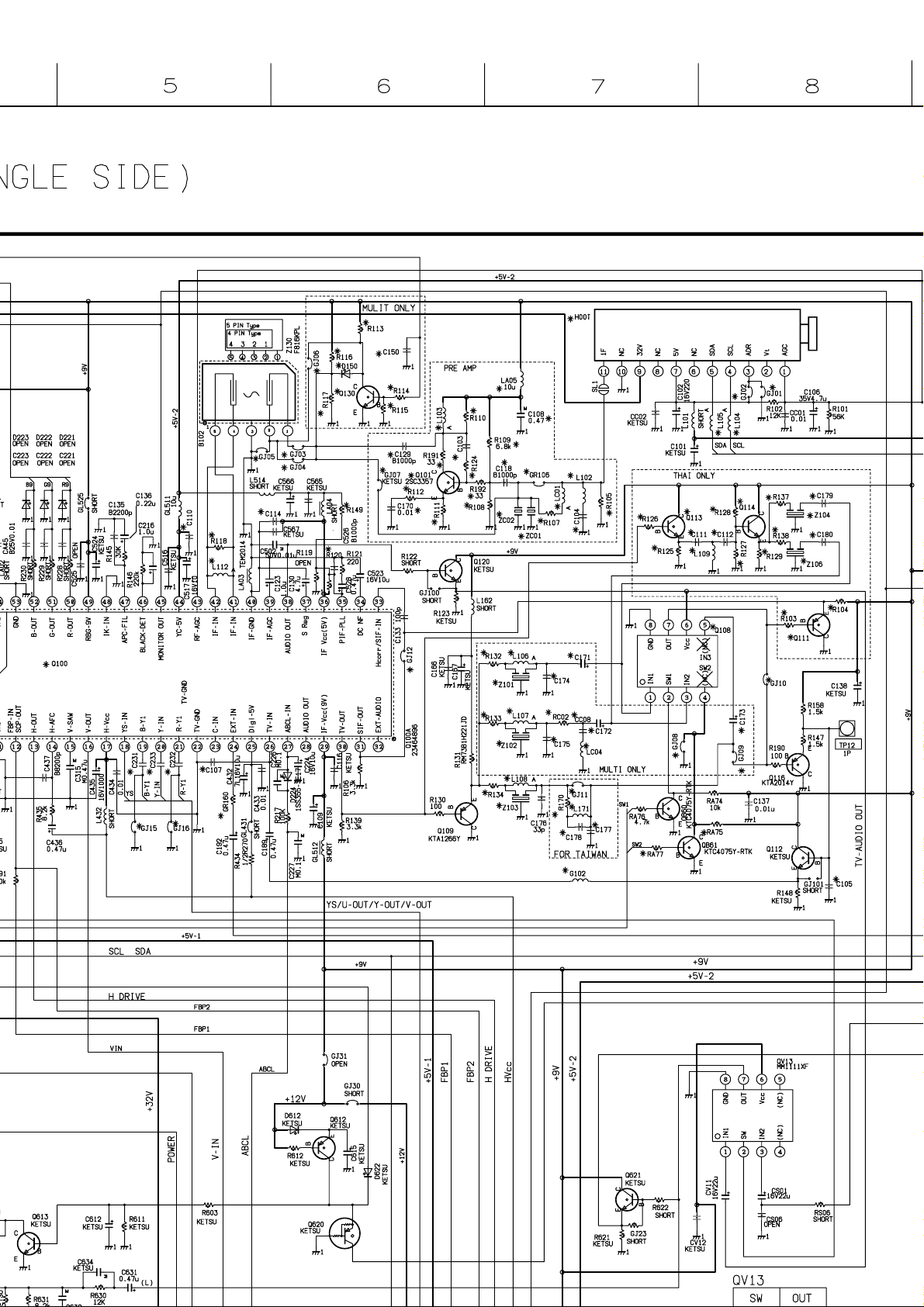
SCHEMATIC DIAGRAM
MODEL : 14SV2M
WARNING: BEFORE SERVICING THIS CHASSIS, READ THE "X-RAY RADIATION PRECAUTION", "SAFETY
PRECAUTION" AND "PRODUCT SAFETY NOTICE" ON THE MANUAL FOR THIS MODEL.
CAUTION: The international hazard symbols " " in the schematic diagram and the parts list designate components
which have special characteristics important for safety and should be replaced only with types identical to those in the
original circuit or specified in the parts list. The mounting position of replacements is to be identical with originals.
Before replacing any of these components, read carefully the PRODUCT SAFETY NOTICE on the MANUAL for this
model. Do not degrade the safety of the receiver through improper servicing.
NOTE:
1. RESISTOR Resistance is shown in ohm [K = 1.000, M = 1.000.000]. All resistors are 1/6W and 5% tolerance
carbon resistor, unless otherwise noted as the following marks.
1/2R = Metal or Metal oxide of 1/2 watt 1/2S = Carbon compsistion of 1/2 watt
1RF = Fuse resistor of 1 watt 10W = Cement of 10 watt
±10% G = ±2% F = ±1%
K =
2. CAPACITOR Unless otherwise noted in schematic, all capacitor values less than 1 are expressed in
the values more than 1 in pF.
All capacitors are ceramic 50V, unless otherwise noted as the following marks.
Electolytic capacitor
Mylar capacitor
µ
F, and
3. The parts indicated with "
4. Voltages read with DIGITAL MULTI-METER from point indicated to chassing ground, using a color bar signal with
all controls at normal, line voltage at 220 volts.
5. Waveforms are taken receiving color bar signal with enough sensitivity.
6. Voltage reading shown are nominal values and may vary ±20% except H.V.
SCHEMATIC DIAGRAM STRUCTURE:
– MAIN / CRT DRIVE (SIGNAL) Circuit ................................................................................................ 1/2
– MAIN (POWER / DEF) Circuit ........................................................................................................... 2/2
" have special characteristics, and should be replaced with identical parts only.
SPECIFIC INFORMATIONS
– 27 –
Page 26

~
~
– +
TUNER
H001
Q100
MICRO PROCESSOR
VIDEO,CHROMA,DEF
Q840
5V-1
REGULATOR
RESET
+32V
Q801
Q862
Q404
Q301
Q901,Q903,Q905
Q610
AV IN
FRONT
AV IN
BACK
HYBRID
CONVERTER TRANS.
+B VOLTAGE
VIDEO OUT
V. OUT
H. OUT
F.B.T.
H.V.
D.Y.
V
H
CRT
AUDIO OUT
W661
HEADPHONE
JACK
*
*
*
BUS CONTROL BLOCK
V
A
MONITOR
OUTPUT
V
A
V
A
P661
SPECIFIC INFORMATIONS
MEMORY
*
QA02
POWER MUTE
CIRCUIT BLOCK DIAGRAM
PV01
AV SW
QV13
PV02
D801-D804
– 28 –
Page 27

SPECIFICATIONS
MODEL
Rated voltage
Power consumption
(at ~ 220V 50Hz)
Dimensions
(Width x Depth x Height)
Mass
Picture Tube Type 21
Television system Channel
(Aerial input) coverage
Special RF Color system Sound system
signal NTSC4.43 5.5/6.0/6.5 MHz
Color system PAL / SECAM / NTSC4.43 / NTSC3.58
Sound output 5W
Terminals Input : Video/Audio (monaural)
Speaker
System Channel VHF UHF CATV
PAL B/G CCIR 2 - 12 21 - 69 X~Z+2, S1~S41
PAL I UK –– 21 - 69 ––
PAL D/K CHINA 1 -12 13 - 57 Z-1~ Z-38
SECAM B/G CCIR 2 - 12 21 - 69 X~Z+2, S1~S41
SECAM D/K OIRT 1 -12 21 - 69 X1~X19
NTSC M US 2 -13 14 - 69 A-6~A-1, A~W, AA~ZZ, AAA, BBB
NTSC M JAPAN 1 -12 13 - 62 M1~M10, S1~41
PAL 60 Hz 5.5/6.0/6.5 MHz
Monitor output : Video/Audio (monaural)
(372.5mm) Overall picture tube measured diagonally
(335.4mm) Viewable picture tube measured diagonally
90° deflection
~ 110 - 240V, 50/60Hz
478.0(W) X 375.0(D) X 362.0(H) mm
SPECIFIC INFORMATIONS
14SV2M
60W
10.1kg
6 x 12cm (2)
* Please refer to owner's manual in detail.
– 29 –
– END –
Page 28

TOSHIBA CORPORATION
Page 29

SCHEMATIC DIAGRAM
MODEL : 14SV2M
WARNING: BEFORE SERVICING THIS CHASSIS, READ THE "X-RAY RADIATION PRECAUTION", "SAFETY
PRECAUTION" AND "PRODUCT SAFETY NOTICE" ON THE MANUAL FOR THIS MODEL.
CAUTION: The international hazard symbols " " in the schematic diagram and the parts list designate components
which have special characteristics important for safety and should be replaced only with types identical to those in the
original circuit or specified in the parts list. The mounting position of replacements is to be identical with originals.
Before replacing any of these components, read carefully the PRODUCT SAFETY NOTICE on the MANUAL for this
model. Do not degrade the safety of the receiver through improper servicing.
NOTE:
1. RESISTOR Resistance is shown in ohm [K = 1.000, M = 1.000.000]. All resistors are 1/6W and 5% tolerance
carbon resistor, unless otherwise noted as the following marks.
1/2R = Metal or Metal oxide of 1/2 watt 1/2S = Carbon compsistion of 1/2 watt
1RF = Fuse resistor of 1 watt 10W = Cement of 10 watt
±10% G = ±2% F = ±1%
K =
2. CAPACITOR Unless otherwise noted in schematic, all capacitor values less than 1 are expressed in
the values more than 1 in pF.
All capacitors are ceramic 50V, unless otherwise noted as the following marks.
Electolytic capacitor
Mylar capacitor
µ
F, and
3. The parts indicated with "
4. Voltages read with DIGITAL MULTI-METER from point indicated to chassing ground, using a color bar signal with
all controls at normal, line voltage at 220 volts.
5. Waveforms are taken receiving color bar signal with enough sensitivity.
6. Voltage reading shown are nominal values and may vary ±20% except H.V.
SCHEMATIC DIAGRAM STRUCTURE:
– MAIN / CRT DRIVE (SIGNAL) Circuit ................................................................................................ 1/2
– MAIN (POWER / DEF) Circuit ........................................................................................................... 2/2
" have special characteristics, and should be replaced with identical parts only.
– 27 –
Page 30

~
~
– +
TUNER
H001
Q100
MICRO PROCESSOR
VIDEO,CHROMA,DEF
Q840
5V-1
REGULATOR
RESET
+32V
Q801
Q862
Q404
Q301
Q901,Q903,Q905
Q610
AV IN
FRONT
AV IN
BACK
HYBRID
CONVERTER TRANS.
+B VOLTAGE
VIDEO OUT
V. OUT
H. OUT
F.B.T.
H.V.
D.Y.
V
H
CRT
AUDIO OUT
W661
HEADPHONE
JACK
*
*
*
BUS CONTROL BLOCK
V
A
MONITOR
OUTPUT
V
A
V
A
P661
SPECIFIC INFORMATIONS
MEMORY
*
QA02
POWER MUTE
CIRCUIT BLOCK DIAGRAM
PV01
AV SW
QV13
PV02
D801-D804
– 28 –
Page 31

14SV2M
MAIN (SIGNAL)
(1/2)
Page 32

Page 33
Page 34

Page 35

Page 36

Page 37

Page 38

Page 39

14SV2M
MAIN (SIGNAL)
(1/2)
Page 40

14SV2M
MAIN (POW/DEF)
(2/2)
Page 41

Page 42

Page 43

Page 44

Page 45

Page 46

Page 47

Page 48

14SV2M
MAIN (POW/DEF)
(2/2)
 Loading...