

TORISAN TM133XG-02L07 Specification
NOTICES
1. The contents st ated in t his doc ument an d the pr od uct may be s ubject to c hang e
without prior notice.
When you kindly study to use this product, please ask our distributor or us for
the latest information.
2. This product is developed and produced for usage onto normal electronic
products (office automation equipments, communication peripherals, electric
appliance products, game machines, etc.) and is not suitable for applications
which need extremely high reliability and extreme safety (aero- or space-use
machines, control eq ui p ments for nuclear p ower , l if e ke eping equipments, etc.).
3. This document shall not grant or guarantee any right to adapt intellectual
property or any other patents of third party.
4. Please use this product correctly according to operating conditions and
precautions for use stated in this document.
Please install safety proof in your designing to avoid human accident, fire
accident and social damage, which may be resulted from malfunction of this
product.
5. This product is not designed to withstand against radiant rays.
6. It is strictly prohibited to copy or publish a part or whole of this document
without our prior written approval.
REVISION HISTORY
DATE REVISION NO. PAGE DESCRIPTIONS
Feb. 15, 01 Ver. 1 - Initial Release
May . 17, 01 Ver. 2 3 OPTICAL CHARACTERISTICS
Brightness : MIN - à 100
Measurement points
the average of 5 points à center (1 poi nt )
Brightness unifor mity : TYP - à (1.35)
4 BACKLIGHT CHARACTERISTICS
Lamp volta ge : TYP TBD à (620)
Start up voltage : MAX TBD à (1350)
Tottori SANYO Electric Co., Ltd. TM133XG-02L07 Ver.2
Page
1/16
MECHANICAL CHARACTERISTICS
Ta=25 degC
ITEM SPECIFICATION UNIT
Module size 284.0(W) x 214.5(H) x 5.5 Max.(t) mm
Resolution 1024 x R.G.B(W) x 768(H) pixel
Sub-pixel pitch 0.088(W) x 0.264(H) mm
Pixel pitch 0.264(W) x 0.264(H) mm
Active area 270.336(W) x 202.752(H) mm
Effective viewing area 272.2(W) x 204.6(H) Min. mm
Bezel opening area 274.2(W) x 206.6(H) mm
Weight (360) Ty p. g
ELECTRICAL ABSOLUTE MAXIMUM RATINGS
Ta=25 degC
ITEM SYMBOL MIN MAX UNIT NOTE
Power supply voltage VDD-VSS -0.3 4.0 V
Input voltage VI VSS-0.3 VDD+0.3 V
Lamp current IL -7.0mA
Lamp supply voltage
VHV - 2000 Vrms
V
LGND - 100 Vrms
ENVIRONMENTAL ABSOLUTE MAXIMUM RATINGS
Ta=25 degC
ITEM SYMBOL CONDITIONS MIN MAX UNIT NOTE
TST Storage -20 60Ambient
temperature
Humidity - Ta=40 degC max. - 85 %RH No condensation
Vibration - St orage - 1.5 G Note 3
Shock - Storage - 50 G XYZ 11ms/direction
OP Operation 0 50
T
degC Note 1
Note 2
[Note 1] Care should be taken so that the LCD module may not be subjected to the
temperature beyond this specification.
[Note 2] Ta>40 degC: Absolute humidity shall be less than that of 85%RH/40 degC.
[Note 3] 10-200Hz, 30min/cycle, X/Y/Z each one cycle and except for resonant frequency.
ELECTRICAL CHARACTERISTICS
VDD=3.3V ,fV=60Hz ,fCLK=65MHz ,Ta=25 degC
ITEM SYMBOL CONDITIONS MIN TYP MAX UNIT NOTE
Power supply voltage VDD-VSS 3.0 3.3 3.6 V
L VDS input
Threshold voltage
L VDS input
Termination resistor
Power Supply current IDD Note 1 - (350) (600) mA
VTH High level - - +100
TL Low level -100 - -
V
T - 100 - ohms Internal
R
mV V
CM=1.2V
[Note 1] Under the following display image :
Typical Value: Display pattern is 64 gray scale bar.
[Note 2] V
CM : Common mode voltage of LVDS input
Tottori SANYO Electric Co., Ltd. TM133XG-02L07 Ver.2
Page
2/16
OPTICAL CHARACTERISTICS
r
δ
ITEM SYMBOL CONDITIONS MIN TYP MAX UNIT NOTE
Brightness B
Brightness unifor mity
δB
Contrast ratio CR
Viewing angle range CR>10
Response
Color of CIE
Coordinate
Rise tr - (32) 50
time
Fall tf
Red
Green
Blue
White
xyxyxyx
y
φ =0 deg.
φ =0 deg.
φ =0 deg.
φ =0 deg.
φ =0 deg.
θ = 0 deg.
θ = 90 deg.
θ =180 deg.
θ =270 deg.
Ta=25 degC, VDD=3.3V, fV=60Hz
2
100 (150) -
cd/m
Note 4,6,7
- (1.35) 1.45 - Note 5,6,7
(150) (300) - - Note 2,4,7
30 - 40 - 10 - -
deg.
Note 1,2,
4,7
40 - -
- (13) 30
(0.58)
(0.35)
(0.31)
(0.56)
(0.15)
(0.11)
0.283 0.313 0.343
0.299 0.329 0.359
ms. Note 3,4,7
-
-
-
-
-
- Note 4,7
-
φφφφ
θθθθ
=180
B
θθθθ
=270
θθθθ
[Note 1] and [Note 3] Response time
φφφφ
θθθθ
=0
θθθθ
θθθθ
=90
Black Black
100%
90%
10%
0%
t
WhiteDATA
[Note 2] The contrast ratio "CR" is defined as :
Brightness at White
CR =
Brightness at Black
[Note 4] This shall be measured at center (point No.3 shown in Note 6).
tf
[Note 5] The brightness uniformity "
δB" is defined as :
Maximum brightness of five points
B =
Minimum brightness of five points
Tottori SANYO Electric Co., Ltd. TM133XG-02L07 Ver.2
Page
3/16

[Note 6] Measurement points
p
A
1/6Vp
5/6Hp1/2Hp1/6Hp
ctive area
12
1/2Vp
5/6Vp
4
3
5
Vp: Total Number of Ve r tical pixel
: Total Number of horizontal pixel
H
[Note 7] Measurement condition
(1) Measurement equipment: BM-5A (TOPCON Corp.), Field=2 degree
(2) Ambient temperature Ta: 25 +/- 2 degC
(3) LCD: All pixels are WHITE, V
DD=3.3V, fV=60Hz
(4) Measure after 30 minutes of CFL warm up.
L=6.0 mArms with the Lamp inverter CXA-L0612A-VJL (TDK).
(5) I
BACKLIGHT CHARACTERISTICS
Ta=25 degC
ITEM SYM. CONDITIOS MIN TYP MAX UNIT NOTE
Lamp voltage VL - (620) - Vr ms at IL=6.0mArms
Lamp current IL 3.0 - (6.5) mArms
Operating frequency fL 40 60 65 kHz
Start up voltage VS - - (1350) Vrms at Ta=0 degC
Lamp life time tOL (10000) - - hrs at IL=6.0 mArms
[Note 1] Backlight driving conditions (operating frequency fL especially) may interfere with
horizontal frequency f
Therefore the operating frequency f
frequency f
H to avoid interference.
H, causing the beat or flicker on the display.
L shall be adjusted in relation to horizontal
(Recommended value)
(Recommended value)
[Note 2] The inverter open voltage should be larger than start up voltage, otherwise backlight
may blinking for a moment after turns on or not be turned on.
And this voltage should be applied to lamp for more than 1 second to start up,
otherwise backlight may not be turned on.
[Note 3] If driving current waveform is asymmetrical, mercury deviation inside of CFL will
incline to one side and consequently abnormal lighting may occur.
To prevent such unfavorable lighting, driving current waveform is asked to have
unbalance rate of less than 10% and wave-height rate of less than 2 +/- 10%.
And this driving waveform shall be confirmed in your system.
Unbalance rate = | Ip - I-p | / IL x 100 (%)
Ip
I-p
Current waveform
Wave-height rate = I
Ip : High peak value
I
-p : Low peak value
I
L : Effective value
p (or I-p) / IL
[Note 4] The inverter of ground reference type should be used. The inverter of ground floating
type should not be used.
Tottori SANYO Electric Co., Ltd. TM133XG-02L07 Ver.2
Page
4/16
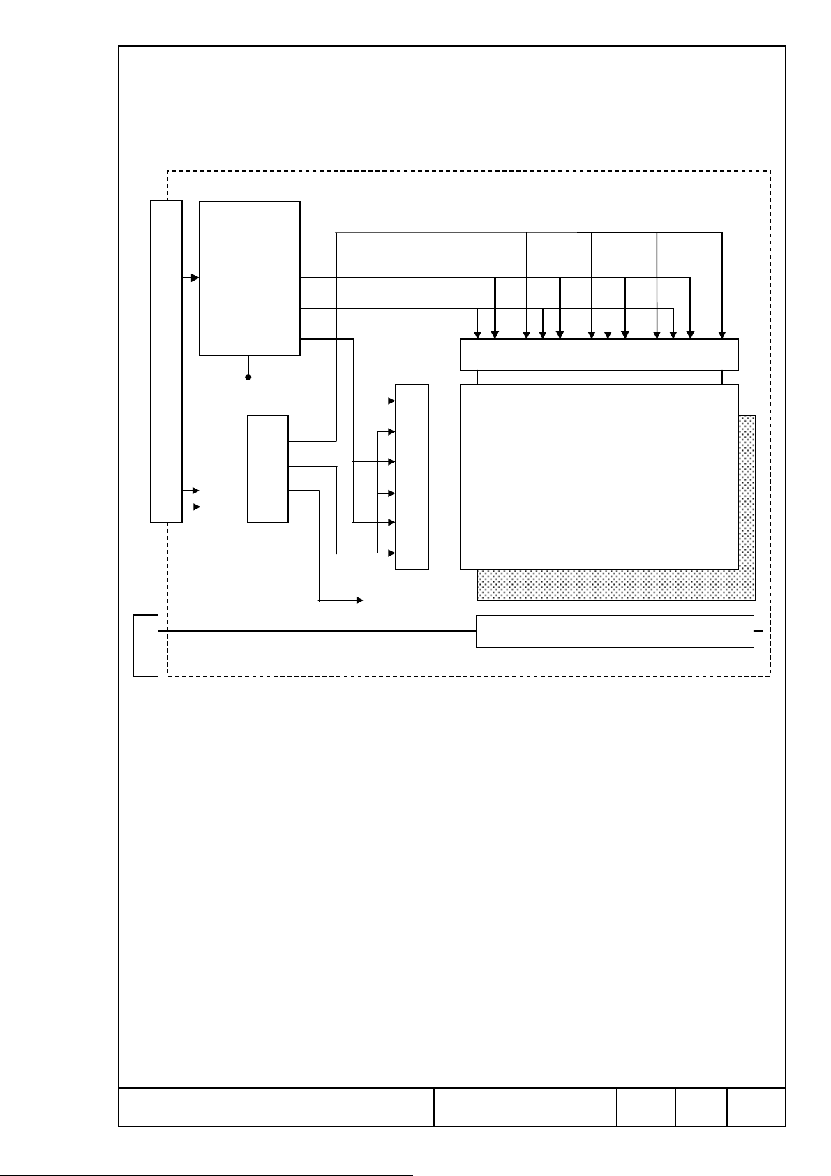
BLOCK DIAGRAM
r
ASIC
TFT Timi ng
Generator
(LVDS-Receiver)
CN1
DE
DATA
Source Driver
1024 x (RGB)
VDD
DC/DC
VSS
FLCN1
Converter
Vcom
Gate Drive
768
TFT Panel
Back Light
Lamp
Tottori SANYO Electric Co., Ltd. TM133XG-02L07 Ver.2
Page
5/16
 Loading...