

Torex Semiconductor Ltd XP132A01A0SR Datasheet
373
XP132A01A0SR
PowerMOSFET
u
8D1S
5D4G
6D3S
7D2S
◆ P-Channel Power MOS FET
◆ DMOS Structure
◆ Low On-State Resistance: 0.105Ω MAX
◆ Ultra High-Speed Switching
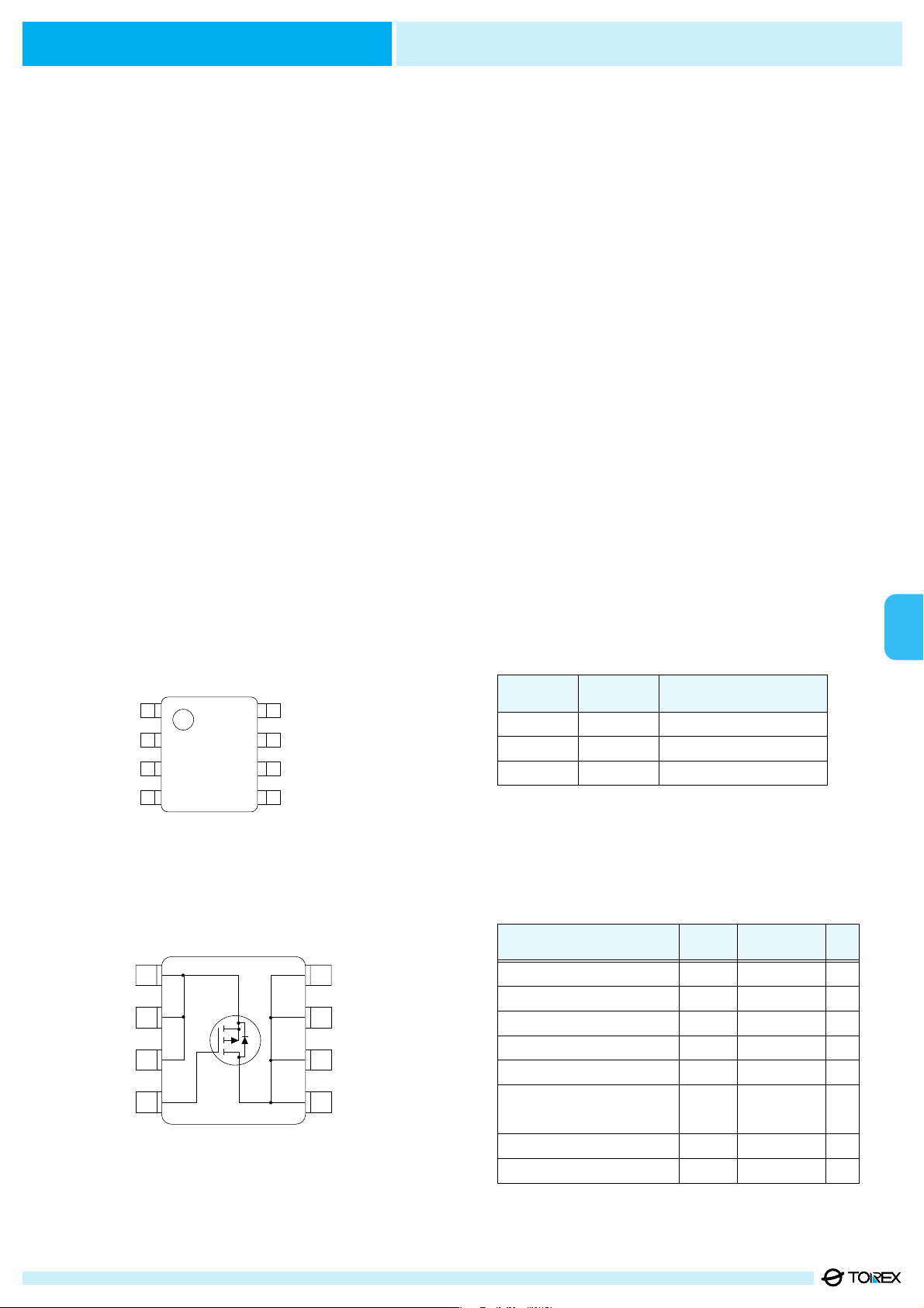
◆ SOP-8 Package
■ Applications
● Notebook PCs
● Cellular and portable phones
● On-board power supplies
● Li-ion battery systems
■ General Description
The XP132A01A0SR is a P-Channel Power MOS FET with low on-state
resistance and ultra high-speed switching characteristics.
Because high-speed switching is possible, the IC can be efficiently set
thereby saving energy.
The small SOP-8 package makes high density mounting possible.
■ Features
Low on-state resistance: Rds(on)=0.075Ω(Vgs=-10V)
Rds(on)=0.105Ω(Vgs=-5.5V)
Ultra high-speed switching
Operational Voltage: -5.5V
High density mounting: SOP-8
■ Absolute Maximum Ratings
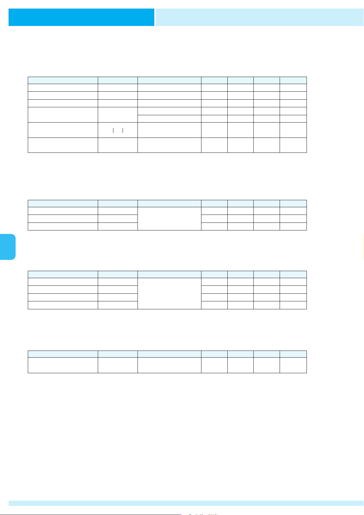
■ Equivalent Circuit
■ Pin Configuration
P-Channel MOS FET
(1 device built-in)
PARAMETER
Drain-Source Voltage
Gate-Source Voltage
Drain Current (DC)
Drain Current (Pulse)
Reverse Drain Current
Continuous Channel
Power Dissipation (note)
Channel Temperature
Storage Temperature
Vdss
Vgss
Id
Idp
Idr
Pd
Tch
Tstg
-30
±20
-5
-15
-5
2.5
150
-55~150
V
V
A
A
A
W
:
:
SYMBOL RATINGS
UNITS
■ Pin Assignment
PIN
NUMBER
PIN
NAME
FUNCTION
1~3
5~8
4
S
D
G
Source
Drain
Gate
81
54
63
72
SOP-8
(TOP VIEW)
Ta=25
:
When implemented on a glass epoxy PCB
Note:
XP132A01A0SR
PowerMOSFET
374
u
DC characteristics
Ta=25
:
■ Electrical Characteristics
PARAMETER UNITS
Gate-Source Cut-off Voltage Vgs(off) -1.0 -2.5
V
0.105Id=-1A, Vgs=-5.5V Ω
Gate-Source Leakage Current Igss µA±10
Forward Transfer Admittance
(note)
5S
Body Drain Diode
Forward Voltage
-0.85 -1.1 V
Drain Cut-off Current Idss -10 µA
Vf
Vds=-30V, Vgs=0V
Id=-1mA, Vds=-10V
Id=-3A, Vds=-10V
If=-5A, Vgs=0V
Vgs=±20V, Vds=0V
Drain-Source On-state
Resistance (note)
Rds(on)
Ω
Id=-3A, Vgs=-10V
0.075
SYMBOL CONDITIONS MAXMIN TYP
PARAMETER UNITS
Feedback Capacitance Crss
pF
Output Capacitance Coss pF
Input Capacitance Ciss
200
560
780 pF
Vds=-10V, Vgs=0V
f=1MHz
SYMBOL CONDITIONS MAXMIN TYP
Dynamic characteristics
Ta=25
:
Effective during pulse test.
Note:
Yfs
PARAMETER UNITS
Fall Time tf
ns
Rise Time tr ns
Turn-on Delay Time td (on)
20
Turn-off Delay Time td (off)
ns
30
25
20 ns
Vgs=-5V, Id=-3A
Vdd=-10V
SYMBOL CONDITIONS MAXMIN TYP
Switching characteristics
Ta=25
:
PARAMETER UNITS
Rth (ch-a)
Thermal Resistance
(channel-surroundings)
50
˚C/W
Implement on a glass epoxy
resin PCB
SYMBOL CONDITIONS MAXMIN TYP
Thermal characteristics
 Loading...