


Torex Semiconductor Ltd XC6201P602TH, XC6201P602TB, XC6201P592TH, XC6201P592TB, XC6201P592MR Datasheet
...
Series
Positive Voltage Regulators
CMOS Low Power Consumption
Dropout Voltage |
: 0.16V |
@ 100mA, |
|
0.40V |
@ 200mA |
Maximum Output Current : 250mA (VOUT=5.0V, TYP) |
||
Highly Accurate |
: ± 2% |
|
Output Voltage Range : 1.3V ~ 6.0V
SOT-25 / SOT-89 / TO-92 Package
Capacitors can be Tantalum or Ceramic
■General Description
The XC6201 series are highly precise, low power consumption, positive voltage regulators manufactured using CMOS and laser trimming technologies.
The series provides large currents with a significantly small dropout voltage.
The XC6201 consists of a current limiter circuit, a driver transistor, a precision reference voltage and an error amplifier. Output voltage is selectable in 0.1V steps between 1.3V ~ 6.0V.
SOT-25 (250mW), SOT-89 (500mW) and TO-92 (300mW) packages are available.
■Applications
●Mobile phones
●Cordless phones
●Cameras, video recorders
●Portable games 3
●Portable AV equipment
●Reference voltage
●Battery powered equipment
■Features
Maximum Output Current |
: 250mA (TYP.) |
Dropout Voltage |
: 0.16V @ 100mA |
Maximum Operating Voltage |
: 10V |
Output Voltage Range |
: 1.3V ~ 6.0V |
|
(selectable in 0.1V steps) |
Highly Accurate |
: ± 2% |
Low Power Consumption |
: TYP 2.0 A |
Operational Temperature Range : -40°C ~ 85°C |
|
Ultra Small Packages |
: SOT-25 (250mW), |
|
SOT-89 (500mW), |
|
TO-92 (300mW) |
Capacitors can be Tantalum or Ceramic
■Typical Application Circuit |
■Typical Performance |
|||||||
|
|
|
Characteristic |
|
|
|||
VIN |
VOUT |
|
XC6201P332 |
|
|
|
||
|
3.0 |
|
|
|
|
|
||
|
|
|
|
|
|
|
|
|
VSS |
|
A) |
2.5 |
|
|
|
|
|
|
|
|
|
|
|
|
|
|
1.0 F(tantalum) |
1.0 F(tantalum) |
Current:ISS( |
2.0 |
|
|
|
|
|
|
|
|
|
|
|
|||
|
|
1.5 |
|
|
|
|
|
|
|
|
|
|
|
|
|
|
|
|
|
Supply |
1.0 |
|
|
Topr=85°C |
|
|
|
|
|
|
|
25°C |
|
||
|
|
|
|
|
|
|
||
|
|
|
|
|
|
|
|
|
|
|
|
0.5 |
|
|
|
-40°C |
|
|
|
|
|
|
|
|
|
|
|
|
|
0.0 |
|
|
|
|
|
|
|
|
0 |
2 |
4 |
6 |
8 |
10 |
|
|
|
|
|
Input Voltage:VIN(V) |
|
||
185

XC6201 Series
■Pin Configuration
VOUT NC
5 4
|
|
|
|
|
|
|
|
|
|
|
|
|
|
|
|
|
|
|
|
|
|
|
|
|
|
|
|
|
|
|
|
|
|
|
|
|
|
|
|
|
|
|
|
|
|
|
|
|
|
2 |
|
3 |
|
|
2 |
3 |
|
|
|
|
|
|
|
|
|
|
|
|
|
|
|
|
|
|
|
|
|
|
|
|
|
|
|
|
|
|
|
|
|
|
|
|
|
VIN VSS NC |
VOUT |
VSS |
VIN |
|
|
|
|
|
|
|
|
|
|
|||||||
|
|
|
|
SOT-25 |
|
SOT-89 |
|
|
|
|
|
|
|
|
|
|
|
|
||||
3 |
|
|
(TOP VIEW) |
(TOP VIEW) |
1 |
|
2 |
|
3 |
|
1 |
2 |
|
3 |
|
|||||||
|
|
|
|
|
|
|
|
|
|
|
|
|
|
|
||||||||
|
|
|
|
|
|
|
|
|
|
|
|
|
|
|
|
|
|
|
|
|
||
|
|
|
|
|
|
|
|
|
|
|
VOUT VSS VIN |
VSS VOUT VIN |
||||||||||
|
|
|
|
|
|
|
|
|
|
|
|
TO-92 T Type |
TO-92 (L Type) |
|||||||||
|
|
|
|
|
|
|
|
|
|
|
|
TOP VIEW |
(TOP VIEW) |
|||||||||
■Pin Assignment |
|
|
|
|
|
|
|
|
|
|
|
|
|
|||||||||
|
|
|
|
|
|
|
|
|
|
|
|
|
|
|
|
|
|
|
|
|
|
|
|
|
|
|
|
|
|
|
|
PIN NUMBER |
|
|
|
|
|
|
|
|
|
|
|
|
|
|
|
|
|
SOT-25 |
SOT-89/TO-92 T TO-92 L |
|
PIN NAME |
|
|
FUNCTION |
||||||||||||
|
|
|
|
|
|
|
|
|
|
|
|
|
|
|
||||||||
|
5 |
|
|
|
1 |
|
2 |
|
VOUT |
|
|
|
|
|
Output |
|||||||
|
|
|
|
|
|
|
|
|
|
|
|
|
|
|
|
|
|
|
|
|||
|
2 |
|
|
|
2 |
|
1 |
|
VSS |
|
|
|
|
|
Ground |
|||||||
|
|
|
|
|
|
|
|
|
|
|
|
|
|
|
|
|
|
|
|
|||
|
1 |
|
|
|
3 |
|
3 |
|
|
VIN |
|
|
|
|
Power Input |
|||||||
|
|
|
|
|
|
|
|
|
|
|
|
|
|
|
|
|
|
|
|
|||
|
3 |
|
|
|
|
|
|
|
NC |
|
|
No Connection |
||||||||||
|
|
|
|
|
|
|
|
|
|
|
|
|
|
|
|
|
|
|
|
|||
|
4 |
|
|
|
|
|
|
|
NC |
|
|
No Connection |
||||||||||
|
|
|
|
|
|
|
|
|
|
|
|
|
|
|
|
|
|
|
|
|
|
|
■Product Classification
●Ordering Information
X C 6 2 0 1 P erty
↑ ↑
qw
DESIGNATOR |
SYMBOL |
DESCRIPTION |
|
DESIGNATOR |
SYMBOL |
DESCRIPTION |
|
||
q |
01 |
Indicates the |
|
|
|
Output Voltage Accuracy |
|
||
product number |
|
r |
1/2 |
e.g.1 : ±1.0% |
|
||||
w |
P |
Type of |
|
|
|
|
2 : ±2.0% |
|
|
regulator 3-pin |
|
|
M |
Package Type SOT-25 |
|
||||
|
|
|
|
|
|||||
|
|
|
|
|
|
|
|
|
|
|
|
|
|
|
t |
P |
|
SOT-89 |
|
|
|
Output Voltage |
|
T |
|
TO-92 Standard |
|
||
|
|
|
|
|
|
||||
|
|
|
|
L |
|
TO-92 Custom pin configuration |
|||
e |
13 60 |
e.g. 30 : 3.0V |
|
|
|
|
|||
|
|
|
R |
Embossed Tape:Standard Feed |
|
||||
|
|
50 : 5.0V |
|
|
|||||
|
|
|
y |
L |
Embossed Tape:Reverse Feed |
|
|||
|
|
|
|
|
|||||
|
|
|
|
|
H |
Paper Type TO-92 |
|
||
|
|
|
|
|
|
||||
|
|
|
|
|
|
B |
Bag TO-92 |
|
|
186
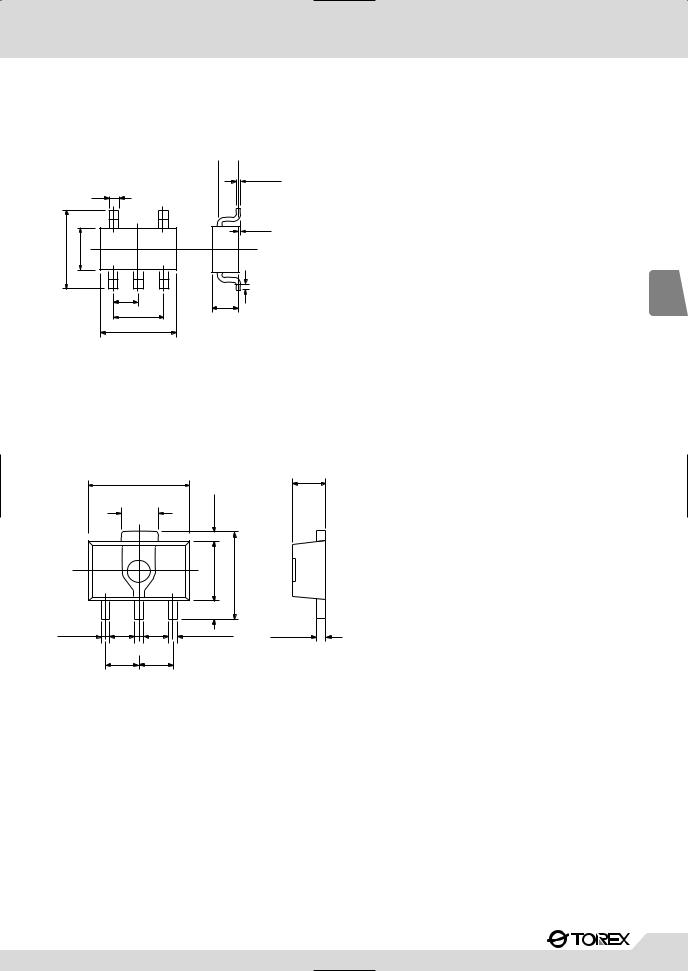
■Packaging Information
●SOT-25
|
|
|
|
0.15 |
+0.1 |
|
|
|
|
-0.05 |
|
|
|
0.4 |
+0.1 |
|
|
|
|
-0.05 |
|
|
|
2.8±0.2 |
1.6 |
|
0 0.1 |
||
|
|
|
|||
|
+0.2 |
-0.1 |
|
|
|
|
|
|
|
0.2min |
|
|
|
0.95 |
1.1±0.1 |
|
|
|
|
|
1.9±0.2 |
|
|
|
|
|
|
|
|
|
|
|
2.9±0.2 |
|
|
●SOT-89
4.5±0.1
1.6 -+0.150.2 |
4 |
|
0. |
|
2.5±0.1 |
4.25max |
|
0.8 |
min |
0.42±0.06 |
0.42±0.06 |
|
|
0.47±0.06 |
|
1.5±0.1
0.4 +0.03-0.02
1.5±0.1 1.5±0.1
XC6201
Series
3
187
XC6201 Series
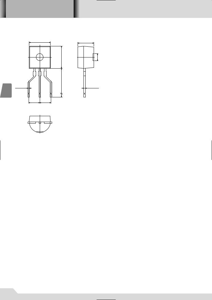
●TO-92
4.65 |
+0.35 |
-0.45 |
|
|
+0.4 -0.5 |
|
4.8 |
3 0.45±0.1 |
10.0min |
|
|
2.5-+00..14 |
2.5 -+00..14 |
3.7±0.3
1.6±0.1
0.4±0.05
188
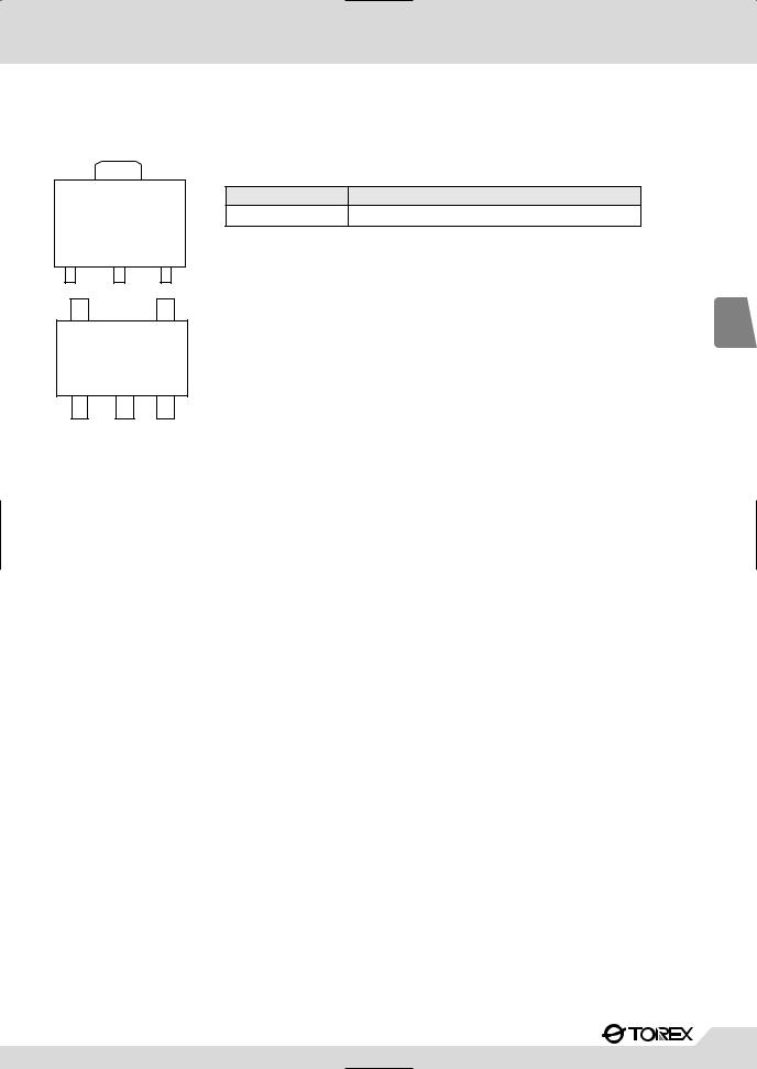
■Marking
●SOT-89, SOT-25
w |
r |
q |
e |
|
SOT-89 |
qwer
SOT-25
XC6201
Series
q Represents the product name
SYMBOL |
PRODUCT NAME |
|
XC6201PXXXXX |
w Represents the type of regulator
|
|
|
|
|
|
|
|
|
|
|
|
|
|
|
|
|
|
|
|
VOLTAGE V |
|
|
0.1 3.0 |
|
3.1 6.0 |
|
6.1 9.0 |
|
|
||||||
|
|
|
|
||||||||||||||
|
|
SYMBOL |
|
|
5 |
|
|
6 |
|
|
|
|
3 |
||||
|
|
e Represents the Output Voltage |
|
|
|
|
|
|
|
|
|||||||
|
|
|
|
|
|
|
|
|
|
|
|||||||
|
|
|
|
|
|
|
|
|
|
|
|||||||
|
|
SYMBOL |
OUTPUT VOLTAGE (V) |
SYMBOL |
OUTPUT VOLTAGE (V) |
|
|
||||||||||
|
0 |
|
|
3.1 |
|
|
|
F |
1.6 |
|
4.6 |
|
|
|
|||
|
1 |
|
|
3.2 |
|
|
|
H |
1.7 |
|
4.7 |
|
|
|
|||
|
2 |
|
|
3.3 |
|
|
|
K |
1.8 |
|
4.8 |
|
|
|
|||
|
3 |
|
|
3.4 |
|
|
|
L |
1.9 |
|
4.9 |
|
|
|
|||
|
4 |
|
|
3.5 |
|
|
|
M |
2.0 |
|
5.0 |
|
|
|
|||
|
5 |
|
|
3.6 |
|
|
|
N |
2.1 |
|
5.1 |
|
|
|
|||
|
6 |
|
|
3.7 |
|
|
|
P |
2.2 |
|
5.2 |
|
|
|
|||
|
7 |
|
|
3.8 |
|
|
|
R |
2.3 |
|
5.3 |
|
|
|
|||
|
8 |
|
|
3.9 |
|
|
|
S |
2.4 |
|
5.4 |
|
|
|
|||
|
9 |
|
|
4.0 |
|
|
|
T |
2.5 |
|
5.5 |
|
|
|
|||
|
|
A |
|
|
4.1 |
|
|
|
U |
2.6 |
|
5.6 |
|
|
|
||
|
|
B |
|
|
4.2 |
|
|
|
V |
2.7 |
|
5.7 |
|
|
|
||
|
|
C |
1.3 |
|
4.3 |
|
|
|
X |
2.8 |
|
5.8 |
|
|
|
||
|
|
D |
1.4 |
|
4.4 |
|
|
|
Y |
2.9 |
|
5.9 |
|
|
|
||
|
|
E |
1.5 |
|
4.5 |
|
|
|
Z |
3.0 |
|
6.0 |
|
|
|
||
|
|
|
|
|
|
|
|
|
|
|
|
|
|
|
|
|
|
r Represents the assembly lot no.
0 9, A Z repeated (G, I, J, O, Q, W excepted)
189
XC6201 Series
●TO-92
q Represents the type of regulator
|
6201 |
6201 |
|
|
|
|
|
|
|
|
|
|
|
|
|||||||||
|
DESIGNATOR |
|
PRODUCT NAME |
|
|
||||||||||||||||||
|
|
|
|
|
|
|
|
|
|
|
|
|
|
|
|||||||||
|
1 2 3 4 |
L |
1 2 3 |
|
4 |
P |
|
|
|
|
XC6201P |
|
|
||||||||||
|
|
T |
|
|
|
|
XC6201T |
|
|
||||||||||||||
|
|
|
|
|
|
|
|
|
|
|
|
|
|
|
|
|
|
||||||
|
5 |
6 |
5 |
|
6 |
|
|
|
|
|
|
|
|
|
|
||||||||
|
|
|
|
|
|
|
|
|
|
|
|
|
|
|
|
|
|
|
|
||||
|
|
|
|
|
|
|
|
|
|
|
|
we Represents the Output Voltage |
|
|
|
|
|||||||
|
|
|
|
|
|
|
|
|
|
|
|
|
|
|
|
|
|
|
|
|
|||
|
|
|
|
|
|
|
|
|
|
|
|
DESIGNATOR |
|
|
|
|
|
|
|
|
|||
|
|
|
|
|
|
|
|
|
|
|
|
|
|
|
|
VOLTAGE V |
|
PRODUCT NAME |
|
|
|||
3 |
|
|
|
|
|
|
|
|
|
|
|
3 |
|
3 |
|
3.3 |
|
XC6201 33 |
|
|
|||
|
|
|
|
|
|
|
|
|
|
|
5 |
|
0 |
|
|
5.0 |
|
XC6201 50 |
|
|
|||
TO-92 L Type |
TO-92 T Type |
|
|
|
|
|
|
|
|
|
|
||||||||||||
|
(TOP VIEW) |
|
(TOP VIEW) |
|
|
|
|
|
|
|
|
|
|
|
|
||||||||
|
|
|
|
|
|
|
|
|
|
|
|
|
|
|
|
|
|
|
|
|
|
||
|
|
|
|
|
|
|
|
|
|
|
|
r Represents the Detect Voltage Accuracy |
|||||||||||
|
|
|
|
|
|
|
|
|
|
|
|
|
|
|
|
|
|
|
|
|
|||
|
|
|
|
|
|
|
|
|
|
|
|
DESIGNATOR DETECT VOLTAGE ACCURACY |
PRODUCT NAME |
|
|||||||||
|
|
|
|
|
|
|
|
|
|
|
|
1 |
|
|
|
within ±1 |
|
XC6201P 1 |
|
|
|||
|
|
|
|
|
|
|
|
|
|
|
|
2 |
|
|
|
|
within ±2 |
|
XC6201P 2 |
|
|
||
|
|
|
|
|
|
|
|
|
|
|
|
|
|
|
|
|
|
|
|
|
|
||
|
|
|
|
|
|
|
|
|
|
|
|
t Represents a least significant digit of the produced year |
|||||||||||
|
|
|
|
|
|
|
|
|
|
|
|
|
|
|
|
|
|
|
|
||||
|
|
|
|
|
|
|
|
|
|
|
|
DESIGNATOR |
|
|
|
Produced year |
|
||||||
|
|
|
|
|
|
|
|
|
|
|
|
|
|
0 |
|
|
|
2000 |
|
||||
|
|
|
|
|
|
|
|
|
|
|
|
|
|
1 |
|
|
|
|
|
2001 |
|
|
|
yDenotes the production lot number
0 to 9, A to Z repeated(G.I.J.O.Q.W excepted)
Note : Character inversion is not used
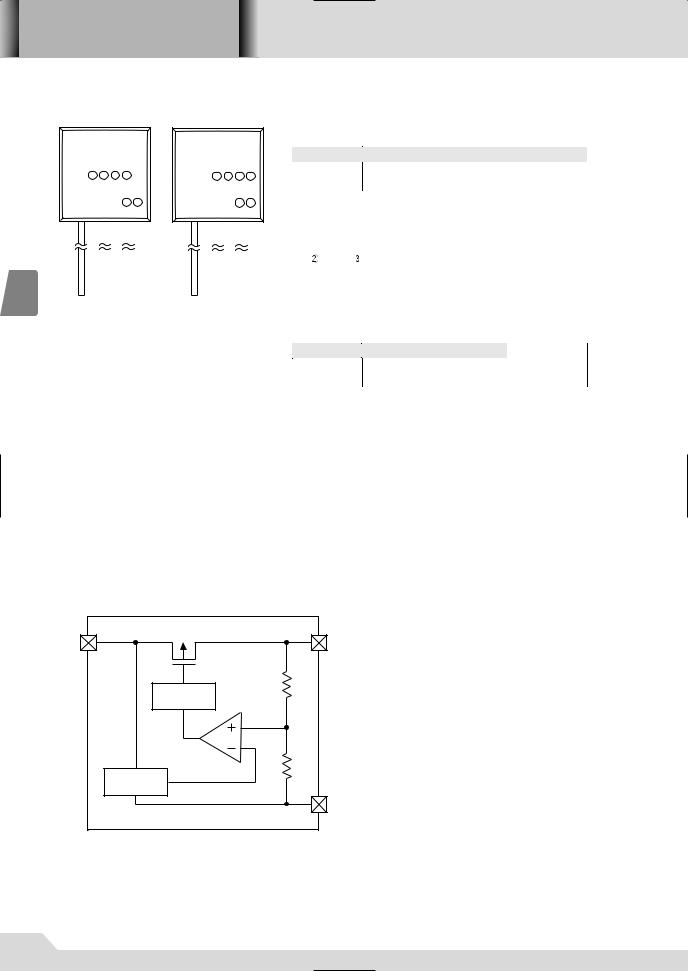
■Block Diagram |
|
VIN |
VOUT |
Current |
|
Limit |
|
Voltage |
|
Reference |
|
|
VSS |
190

■Absolute Maximum Ratings
|
|
|
|
Ta=25°C |
|
PARAMETER |
SYMBOL |
RATINGS |
UNITS |
||
Input Voltage |
VIN |
12 |
|
||
|
|
|
|
|
|
Output Current |
IOUT |
500 |
mA |
||
|
|
|
|
|
|
Output Voltage |
VOUT |
VSS 0.3 VIN 0.3 |
|
||
|
|
|
|
|
|
|
SOT-25 |
|
250 |
|
|
Power |
|
|
|
|
|
SOT-89 |
Pd |
500 |
mW |
||
Dissipation |
|||||
|
|
|
|
||
|
TO-92 |
|
300 |
|
|
|
|
|
|
|
|
Operating Temp. |
Topr |
40 85 |
|
||
|
|
|
|
|
|
Storage Temp. |
Tstg |
55 125 |
|
||
|
|
|
|
|
|
■Electrical Characteristics
XC6201P132 |
VOUT T =1.3V (Note 1) |
|
|
|
|
|
Ta=25°C |
|||
|
|
|
|
|
|
|
|
|
|
|
PARAMETER |
|
SYMBOL |
CONDITIONS |
MIN |
TYP |
MAX |
UNITS |
CIRCUIT |
||
|
|
|
|
VIN 2.3V |
|
|
|
|
|
|
Output Voltage |
|
VOUT(E) (Note2) |
1.274 |
1.300 |
1.326 |
V |
2 |
|||
|
IOUT 10mA |
|||||||||
|
|
|
|
|
|
|
|
|
|
|
|
|
|
|
|
|
|
|
|
|
|
Maximum Output Current |
|
IOUTmax |
VIN 2.3V |
60 |
|
|
mA |
2 |
||
|
VOUT(E)≥1.17V |
|
|
|||||||
|
|
|
|
|
|
|
|
|
|
|
|
|
|
|
|
|
|
|
|
|
|
Load Regulation |
|
ΔVOUT |
VIN 2.3V |
|
10 |
30 |
mV |
2 |
||
|
1mA≤IOUT≤30mA |
|
||||||||
|
|
|
|
|
|
|
|
|
|
|
|
|
|
|
|
|
|
|
|
|
|
Dropout Voltage (Note 3) |
|
Vdif1 |
IOUT 30mA |
|
200 |
600 |
mV |
2 |
||
|
|
|
|
|
|
|
||||
|
Vdif2 |
IOUT 60mA |
|
500 |
810 |
|||||
|
|
|
|
|
|
|||||
Supply Current |
|
ISS |
VIN 2.3V |
|
3.0 |
5.0 |
A |
1 |
||
|
|
|
|
|
|
|
|
|
|
|
Line Regulation |
|
ΔVOUT |
IOUT 10mA |
|
0.2 |
0.3 |
%/V |
2 |
||
|
|
|
2.3V≤VIN≤10.0V |
|
||||||
|
ΔVIN VOUT |
|
||||||||
|
|
|
|
|
|
|
|
|||
|
|
|
|
|
|
|
|
|
|
|
Input Voltage |
|
|
VIN |
|
1.8 |
|
10 |
V |
|
|
Output Voltage |
|
ΔVOUT |
IOUT 40mA |
|
±100 |
|
ppm |
2 |
||
|
|
|
|
|
-40°C≤Topr≤85°C |
|
|
/°C |
||
Temperature Characteristics |
|
ΔTopr VOUT |
|
|
||||||
|
|
|
|
|
||||||
|
|
|
|
|
|
|
|
|
|
|
1 VOUT(T):
2 VOUT(E):
IOUT (VOUT(T)+1.0V)
3 Vdif {VIN1{ 5} VOUT1{ 4}
4 VOUT1:IOUT (VOUT(T)+1.0V) 98%
5 VIN1: VOUT1
XC6201
Series
3
191
 Loading...