

g
A
(*)
XP152A12C0MR-G
ETR1121_003
Power MOSFET
■GENERAL DESCRIPTIO N
The XP152A12C0MR-G is a P-channel Power MOSFET with low on-state resistance and ultra high-speed switching
characteristics.
Because high-speed switching is possible, the IC can be efficiently set thereby saving energy.
In order to counter static, a gate protect diode is built-in.
The small SOT-23 p acka
■APPLICATIONS
●Notebook PCs
●Cellular and portable phones
●On-board power supplies
●Li-ion battery systems
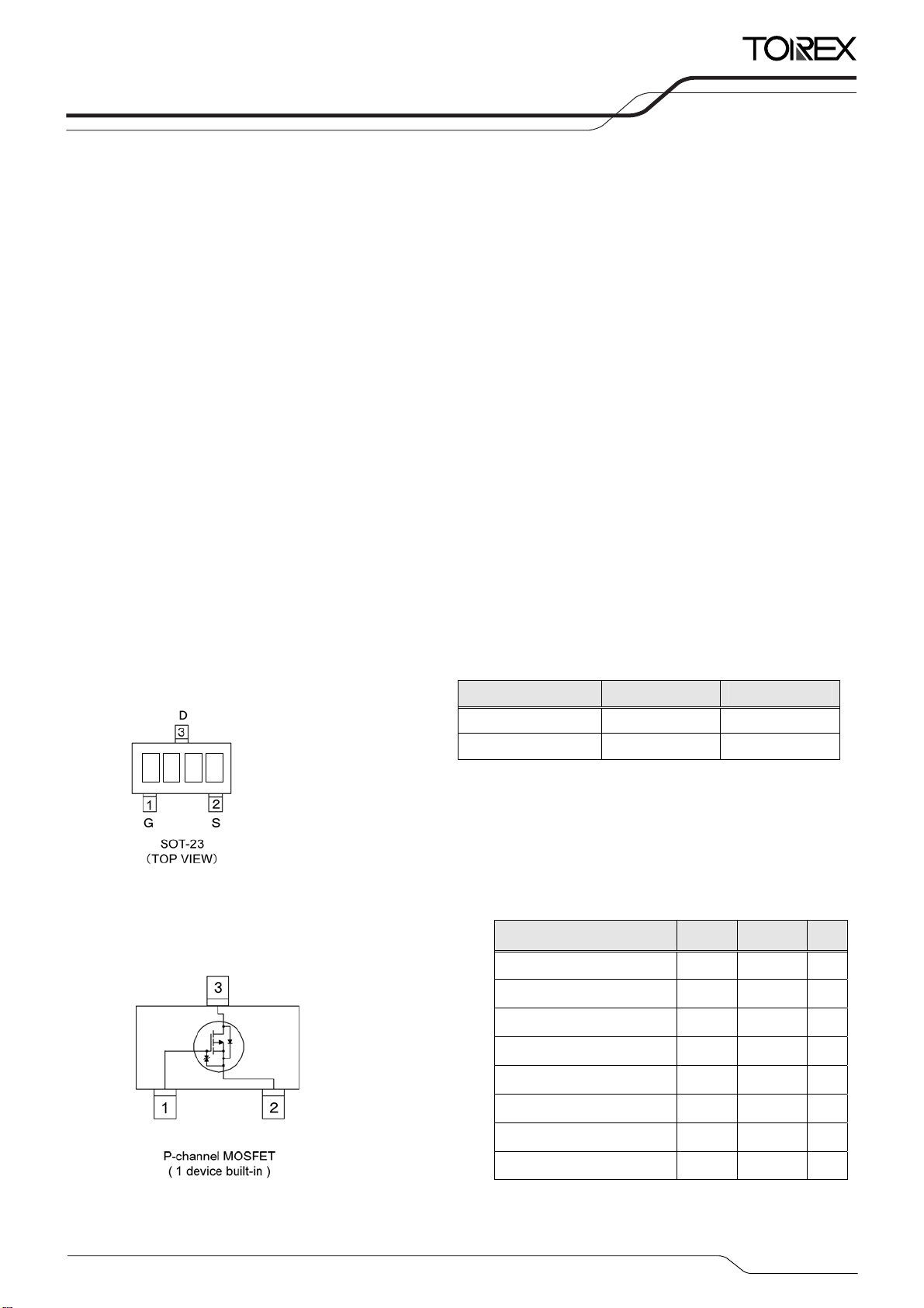
■PIN CONFIGURATION/
MARKING
■EQUIVALENT CIRCUIT
2 1 2
* x represents production lot number.
e makes high density mounting possible.
G:Gate
x
S:Source
D:Drain
■FEATURES
Low On-State Resistance :
:
Ultra High-Speed Switching
Gate Protect Diode Built-in
Driving Voltage : -2.5V
P-Channel Power MOSFET
DMOS Structure
Small Package : SOT-23
Environmentally Friendly : EU RoHS Compliant, Pb Free
Rds(on) = 0.3Ω@ Vgs = -4.5V
Rds(on) = 0.5Ω@ Vgs = -2.5V
■PINASSIGNMENT
PRODUCTS PACKAGE ORDER UNIT
XP152A12C0MR SOT-23 3,000/Reel
XP152A12C0MR-G
The “-G” suffix denotes Halogen and Antimony free as well as
being fully RoHS compliant.
BSOLUTE MAXIMUM RATINGS
■
Drain - Source Voltage Vdss -20 V
Gate - Source Voltage Vgss ±12 V
(*)
PARAMETER SYMBOL RA TINGS UNITS
SOT-23 3,000/Reel
Ta = 25℃
Drain Current (DC) Id -0.7 A
Drain Current (Pulse) Idp -2.8 A
Reverse Drain Current Idr -0.7 A
Channel Power Dissipation *
Channel T emperature Tch 150 ℃
Storage Temperature Tstg -55~150 ℃
* When implemented on a ceramic PCB
Pd 0.5 W
1/5
XP152A12C0MR-G
■ELECTRICAL CHARACTERISTICS
DC Characteristics
PARAMETER SYMBOL CONDITIONS MIN. TYP. MAX. UNITS
Drain Cut-Off Current Idss Vds= -20V, Vgs= 0V - - -10 μA
Gate-Source Leak Current Igss Vgs= ±12V, Vds= 0V - - ±10 μA
Gate-Source Cut-Off Voltage Vgs(off) Id= -1mA, Vds= -10V -0.5 - -1.2 V
Drain-Source On-State Resistance *1
Forward Transfer Admittance *1 | Yfs | Id= -0.4A, Vds= -10V - 1.5 - S
Rds(on)
Id= -0.4A, Vgs= -4.5V - 0.23 0.30 Ω
Id= -0.4A, Vgs= -2.5V - 0.37 0.50 Ω
Ta = 25℃
Body Drain Diode
Forward Voltage
*1 Effective during pulse test.
Dynamic Characteristics
PARAMETER SYMBOL CONDITIONS MIN. TYP. MAX. UNITS
Input Capacitance Ciss
Output Capacitance Coss
Feedback Capacitance Crss
Switching Characteristics
PARAMETER SYMBOL CONDITIONS MIN. TYP. MAX. UNITS
Turn-On Delay Time td (on)
Rise Time
Turn-Off Delay T ime td (off)
Fall Time tf
Thermal Characteristics
PARAMETER SYMBOL CONDITIONS MIN. TYP. MAX. UNITS
Vf If= -0.7A, Vgs= 0V - -0.8 -1.1 V
Vds= -10V, Vgs=0V
f= 1MHz
Ta = 25℃
- 180 - pF
- 120 - pF
- 60 - pF
Ta = 25℃
- 5 - ns
tr - 20 - ns
Vgs= -5V, Id= -0.4A
Vdd= -10V
- 55 - ns
- 70 - ns
2/5
Thermal Resistance
(Channel-Ambience)
Rth (ch-a)
Implement on a ceramic PCB
- 250 - ℃/W
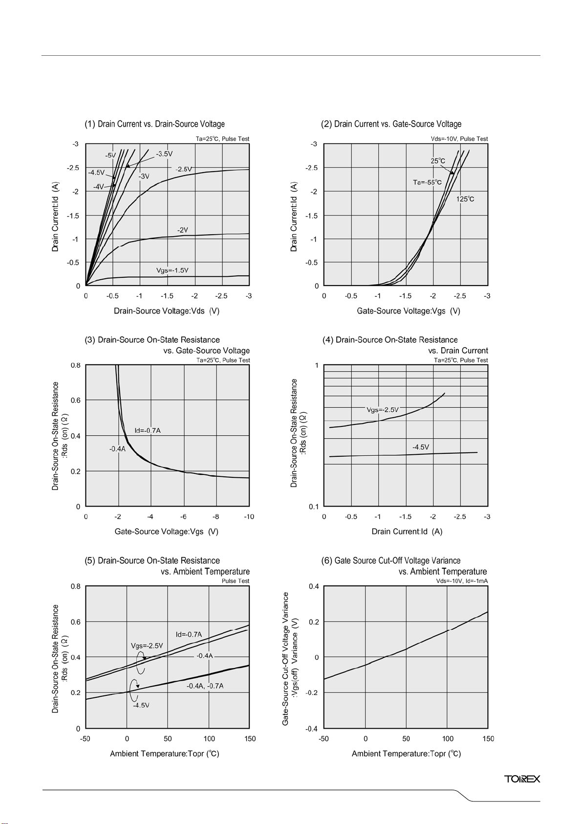
■TYPICAL PERFOMANCE CHARACTERISTICS
XP152A12C0MR-G
3/5

XP152A12C0MR-G
■TYPICAL PERFOMANCE CHARACTERISTICS (Continued)
4/5

XP152A12C0MR-G
1. The products and product specifications contained herein are subject to change without
notice to improve performance characteristics. Consult us, or our representatives
before use, to confirm that the information in this datasheet is up to date.
2. We assume no responsibility for any infringement of patents, patent rights, or other
rights arising from the use of any information and circuitry in this datasheet.
3. Please ensure suitable shipping controls (including fail-safe designs and aging
protection) are in force for equipment employing products listed in this datasheet.
4. The products in this datasheet are not developed, designed, or approved for use with
such equipment whose failure of malfunction can be reasonably expected to directly
endanger the life of, or cause significant injury to, the user.
(e.g. Atomic energy; aerospace; transport; combustion and associated safety
equipment thereof.)
5. Please use the products listed in this datasheet within the specified ranges.
Should you wish to use the products under conditions exceeding the specifications,
please consult us or our representatives.
6. We assume no responsibility for damage or loss due to abnormal us e.
7. All rights reserved. No part of this datasheet may be copied or reproduced without the
prior permission of TOREX SEMICONDUCTOR LTD.
5/5
 Loading...