

TOREX XP151A13A0MR-G User Manual
A
(*)
XP151A13A0MR-G
ETR1119_003
Power MOSFET
■GENERAL DESCRIPTIO N
The XP151A13A0MR-G is an N-channel Power MOSFET with low on state resistance and ultra high-speed switching
characteristics.
Because high-speed switching is possible, the IC can be efficiently set thereby saving energy.
In order to counter static, a gate protect diode is built-in.
The small SOT-23 p ackage makes high density mounting possible.
■APPLICATIONS
●Notebook PCs
●Cellular and portable phones
●On-board power supplies
●Li-ion battery systems
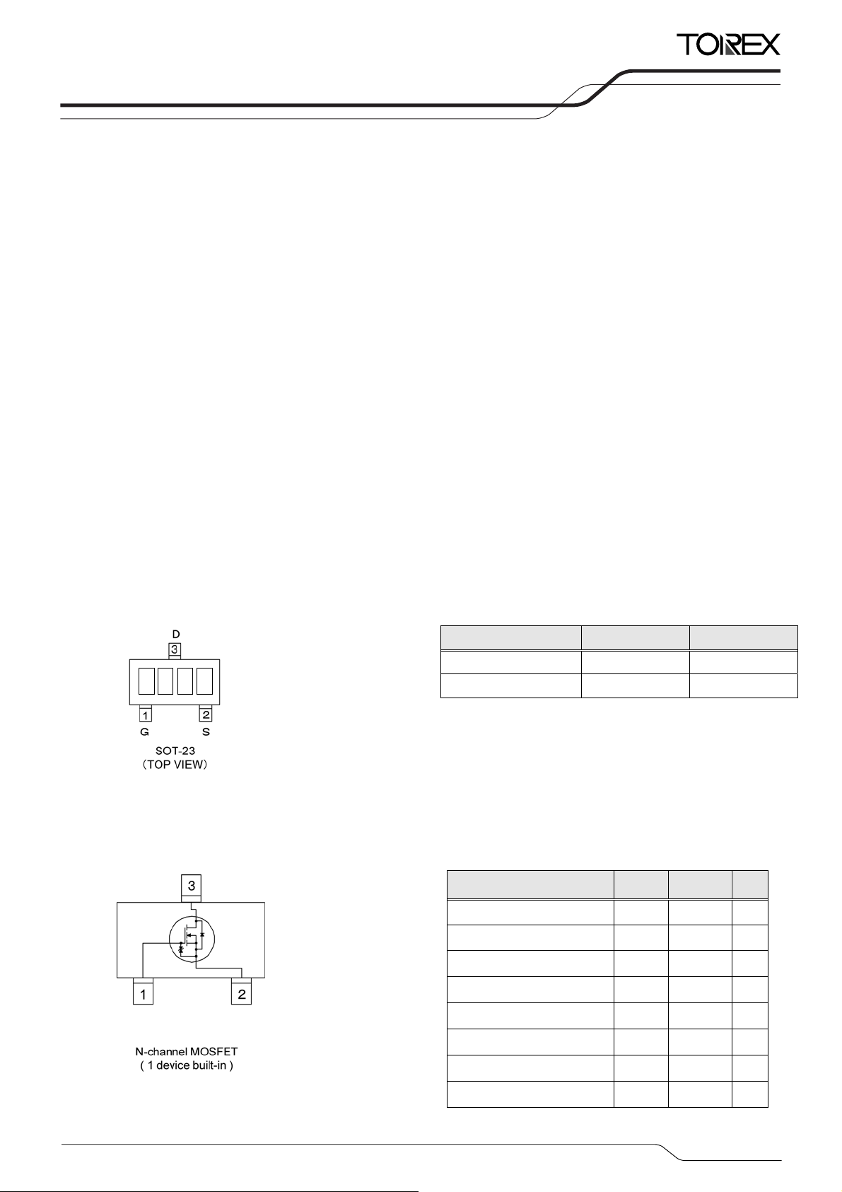
■PIN CONFIGURATION/
MARKING
■EQUIVALENT CIRCUIT
1 1 3
* x represents production lot number.
x
G:Gate
S:Source
D:Drain
■FEATURES
Low On-State Resistance :
:
:
Ultra High-Speed Switching
Gate Protect Diode Built-in
Driving Voltage : 1.5V
N-Channel Power MOSFET
DMOS Structure
Small Package : SOT-23
Environmentally Friendly : EU RoHS Compliant, Pb Free
Rds(on) = 0.1Ω@ Vgs = 4.5V
Rds(on) = 0.14Ω@ Vgs = 2.5V
Rds(on) = 0.25Ω@ Vgs = 1.5V
■PRODUCT NAMES
PRODUCTS PACKAGE ORDER UNIT
XP151A13A0MR
XP151A13A0MR-G
The “-G” suffix denotes Halogen and Antimony free as well as
being fully RoHS compliant.
■
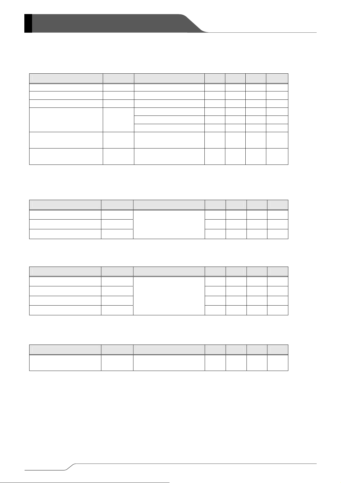
BSOLUTE MAXIMUM RATINGS
PARAMETER SYMBOL RA TINGS UNITS
Drain - Source Voltage Vdss 20 V
Gate - Source Voltage Vgss ±8 V
Drain Current (DC) Id 1 A
Drain Current (Pulse) Idp 4 A
Reverse Drain Current Idr 1 A
Channel Power Dissipation *
Channel T emperature Tch 150 ℃
Storage Temperature Tstg -55~150 ℃
* When implemented on a ceramic PCB
(*)
SOT-23 3,000/Reel
SOT-23 3,000/Reel
Ta = 25℃
Pd 0.5 W
1/5
XP151A13A0MR-G
■ELECTRICAL CHARACTERISTICS
DC Characteristics
PARAMETER SYMBOL CONDITIONS MIN. TYP. MAX. UNITS
Drain Cut-Off Current Idss Vds= 20V, Vgs= 0V - - 10 μA
Gate-Source Leak Current Igss Vgs= ±8V, Vds= 0V - - ±10 μA
Gate-Source Cut-Off Voltage Vgs(off) Id= 1mA, Vds= 10V 0.5 - 1.2 V
Id= 0.5A, Vgs= 4.5V - 0.075 0.100 Ω
Drain-Source On-State Resistance *1
Forward Transfer Admittance *1 | Yfs | Id= 0.5A, Vds= 10V - 4.2 - S
Rds(on)
Id= 0.5A, Vgs= 2.5V - 0.10 0.14 Ω
Id= 0.1A, Vgs= 1.5V - 0.17 0.25 Ω
Ta = 25℃
Body Drain Diode
Forward Voltage
*1 Effective during pulse test.
Dynamic Characteristics
PARAMETER SYMBOL CONDITIONS MIN. TYP. MAX. UNITS
Input Capacitance Ciss
Output Capacitance Coss
Feedback Capacitance Crss
Switching Characteristics
PARAMETER SYMBOL CONDITIONS MIN. TYP. MAX. UNITS
Turn-On Delay Time td (on)
Rise Time
Turn-Off Delay T ime td (off)
Fall Time tf
Thermal Characteristics
PARAMETER SYMBOL CONDITIONS MIN. TYP. MAX. UNITS
Vf If= 1A, Vgs= 0V - 0.8 1.1 V
Vds= 10V, Vgs=0V
f= 1MHz
Ta = 25℃
- 220 - pF
- 120 - pF
- 45 - pF
Ta = 25℃
- 10 - ns
tr - 15 - ns
Vgs= 5V, Id= 0.5A
Vdd= 10V
- 75 - ns
- 65 - ns
2/5
Thermal Resistance
(Channel-Ambience)
Rth (ch-a)
Implement on a ceramic PCB
- 250 - ℃/W
 Loading...