

TOREX XP131A1520SR User Manual
XP131A1520SR
ETR1104_001
Power MOSFET
■GENERAL DESCRIPTION
The XP131A1520SR is an N-channel Power MOSFET with low on-state resistance and ultra high-speed switching
characteristics.
Because high-speed switching is possible, the IC can be efficiently set thereby saving energy.
The small SOP-8 package makes high density mounting possible
■APPLICATIONS
●Notebook PCs
●Cellular and portable phones
●On-board power supplies
●Li-ion battery systems
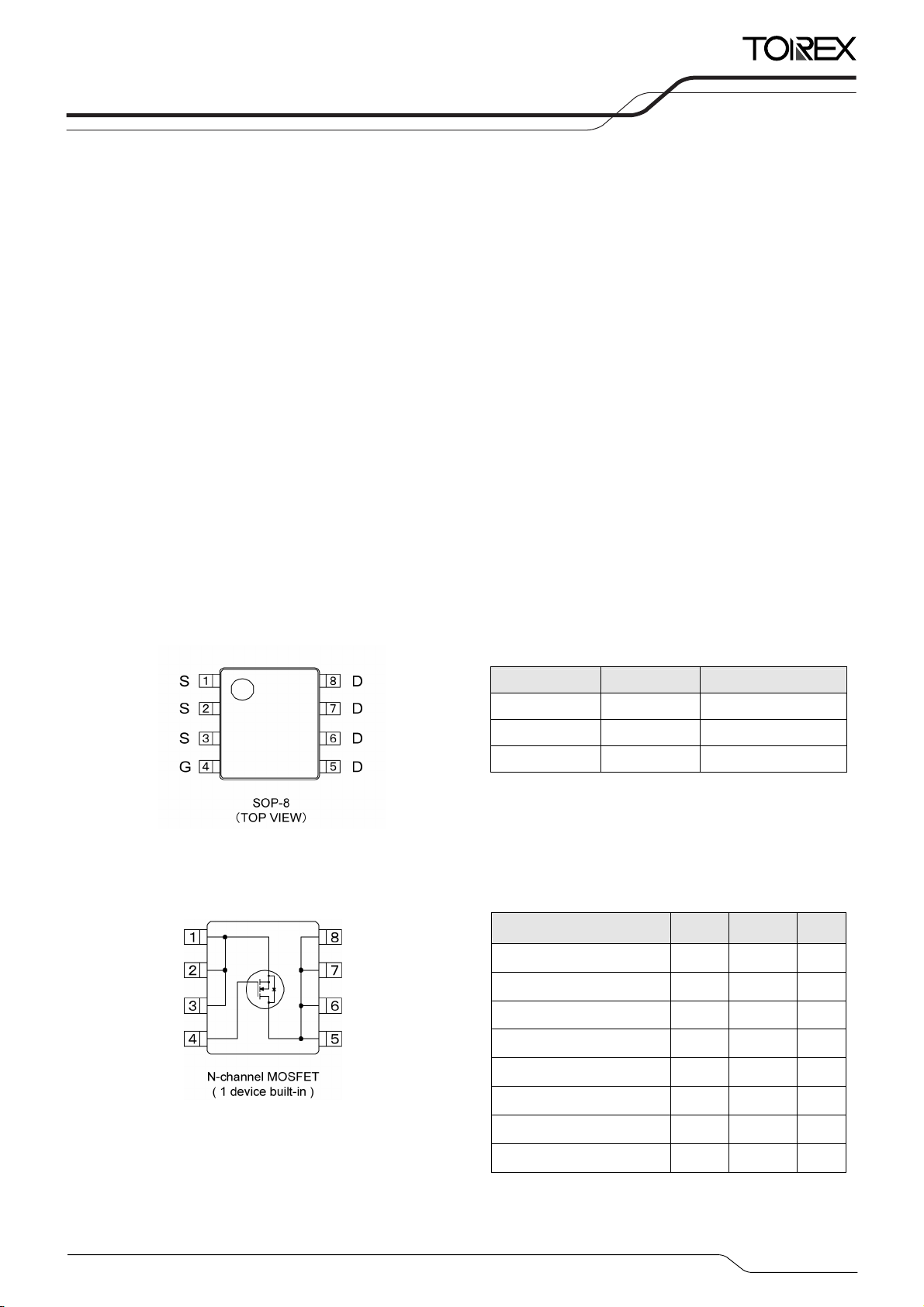
■PIN CONFIGURATION ■PINASSIGNMENT
■EQUIVALENT CIRCUIT
.
■FEATURES
Low On-State Resistance : Rds(on)=0.015(Vgs=10V)
: Rds(on)=0.02Ω(Vgs=4.5V)
Ultra High-Speed Switching
Driving Voltage : 4.5V
N-Channel Power MOSFET
DMOS Structure
Package : SOP-8
PIN NUMBER PIN NAME FUNCTION
1~3 S Source
4 G Gate
5~8 D Drain
■
ABSOLUTE MAXIMUM RATINGS
Ta = 2 5 ℃
PARAMETER SYMBOL RATINGS UNITS
Drain-Source Voltage Vdss 30 V
Gate-Source Voltage Vgss ±20 V
Drain Current (DC) Id 10 A
Drain Current (Pulse) Idp 40 A
Reverse Drain Current Idr 10 A
Channel Power Dissipation *
Channel Temperature Tch 150 ℃
Storage Temperature Range Tstg -55~150 ℃
Pd 2.5 W
* When implemented on a glass epoxy PCB
1/5
XP131A1520SR
■ELECTRICAL CHARACTERISTICS
DC Characteristics
PARAMETER SYMBOL CONDITIONS MIN. TYP. MAX. UNITS
Drain Cut-Off Current Idss Vds=30V, Vgs=0V - - 10
Gate-Source Leak Current Igss Vgs=±20V, Vds=0V - -
Gate-Source Cut-Off Voltage Vgs(off) Id=1mA, Vds=10V 1.0 - 2.5 V
Drain-Source On-State Resistance *
Forward Transfer Admittance * | Yfs | Id=5A, Vds=10V - 20 - S
Body Drain Diode
Forward Voltage
* Effective during pulse test.
Rds(on)
Vf If=10A, Vgs=0V - 0.8 1.1 V
Id=5A, Vgs=10V - 0.012 0.015
Id=5A, Vgs=4.5V - 0.016 0.020
Dynamic Characteristics
PARAMETER SYMBOL CONDITIONS MIN. TYP. MAX. UNITS
Input Capacitance Ciss
Output Capacitance Coss
Feedback Capacitance Crss
Switching Characteristics
PARAMETER SYMBOL CONDITIONS MIN. TYP. MAX. UNITS
Turn-On Delay Time td (on)
Rise Time
Turn-Off Delay Time td (off)
Fall Time tf
Thermal Characteristics
PARAMETER SYMBOL CONDITIONS MIN. TYP. MAX. UNITS
Vds=10V, Vgs=0V
f=1MHz
tr - 25 - ns
Vgs=5V, Id=5A
Vdd=10V
- 1370 - pF
- 740 - pF
- 280 - pF
- 20 - ns
- 40 - ns
- 20 - ns
±
1
Ta = 25℃
μ
A
μ
A
Ω
Ω
Ta = 25℃
Ta = 25℃
2/5
Thermal Resistance
(Channel-Ambience)
Rth (ch-a)
Implement on a glass epoxy
resin PCB
- 50 - ℃/W
 Loading...