


■
■
■
XCM524 Series
ETR2428-003
600mA Synchronous Step-Down DC/DC Converter + 500mA LDO
with Delay Function Voltage Detector
GENERAL DESCRIPTION
The XCM524 series is a multi combination module IC which comprises of a 600mA driver transistor built-in synchronous
step–down DC/DC converter and a high speed, high current LDO regulator with voltage detector function. The device is
housed in small USP-12B01 package which is ideally suited for space conscious applications. The DC/DC converter and the
LDO blocks are isolated in the package so that noise interference from the DC/DC to the LDO regulator is minimal.
The DC/DC converter block with a built-in 0.42ΩP-channel MOS driver transistor and 0.52ΩN-channel MOS switching
transistor, designed to allow the use of ceramic capacitors. The DC/DC enables a high efficiency, stable power supply with an
output current of 600mA to be configured using only a coil and two capacitors connected externally.
The LDO regulator block is precise, low noise, high ripple rejection, low dropout positive voltage regulators with built-in voltage
detector. The LDO is also compatible with low ESR ceramic output capacitors. Good output stability is maintained during
load fluctuations due to its excellent transient response. The current limiter's fold back circuit also operates as a short circuit
protection for the output current.
The voltage detector block of the contains delay circuit. The delay time can be controlled by an external capacitor.
The detector monitors the input voltage of the voltage regulator.
■APPLICATIONS
●BD, DVD drives
●HDD drives
●Cameras, Video recorders
●Mobile phones, Smart phones
●Various general-purpose power supplies
TYPICAL APPLICATION CIRCUIT
(TOP VIEW)
FEATURES
<DC/DC Convertor Block>
Input Voltage Range : 2.7V ~ 6.0V
Output Voltage Options : 0.8V ~ 4.0V (±2%)
High Efficiency : 92% (TYP.)
Output Current : 600mA (MAX.)
Oscillation Frequency : 1.2MHz, 3.0MHz (+15%)
Current Limiter Circuit Built-In : Constant Current & Latching
Control Methods : PWM
PWM/PFM Auto
*Performance depends on external components and wiring on PCB wiring.
<Regulator Block>
Maximum Output Current
Dropout Voltage : 200mV@I
Operating Voltage Range
Output Voltage Options : 0.9V ~ 5.1V (0.1V increments, ±2%)
Detect Voltage Options : 2.0V ~ 5.5V (0.1V increments, ±2%)
VR.VD Temperature Stability :±100ppm/℃ (TYP.)
High Ripple Rejection : 65dB (@10kHz)
Low ESR Capacitor : Ceramic Capacitor
Operating Temperature Range
Package : USP-12B01
Environmentally Friendly : EU RoHS Compliant, Pb Free
: 500mA (Limiter 600mA TYP.)
(2.5V≦V
: 2.0V ~ 6.0V
: -40℃ ~ +85℃
≦4.9V)
ROUT
=100mA (TYP.)
ROUT
1/52

■
■
XCM524 Series
PIN CONFIGURATIOIN
*DC/DC Ground pin (No.5 and 8) should be short before using the IC.
* A dissipation pad on the reverse side of the package should be electrically isolated.
*1: Voltage level of the VDR’s dissipation pad should be V
*2: Voltage level of the DC/DC’s dissipation pad should be V
Care must be taken for an electrical potential of each dissipation pad so as to enhance mounting strength and heat release
when the pad needs to be connected to the circuit.
PIN ASSIGNMENT
PIN No XCM524 FUNCTIONS
1 VDOUT VDR Block: VD Output Voltage
2 VSS VDR Block: Ground
3 Cd VDR Block: Delay Capacitor connection
4 V
5 PGND DC/DC Block: Power Ground
6 Lx DC/DC Block: Switching Connection
7 DCOUT DC/DC Block: Output Voltage
8 AGND DC/DC Block: Analog Ground
9 EN2 DC/DC Block: ON/OFF Control
10 V
11 NC No Connection
12 V
(TOP VIEW)
(BOTTOM VIEW)
SS
DC/DC Block: Power Input
IN2
VDR Block: Power Input
IN1
VDR Block: LDO Output
ROUT
PIN No XCM524 VDR DC/DC
level.
level.
SS
1 V
2 VSS V
3 Cd Cd -
4 V
5 PGND - PGND
6 Lx - Lx
7 DCOUT - VOUT
8 AGND - AGND
9 EN2 - CE
10 V
11 NC - -
12 V
V
DOUT
- VIN
IN2
V
IN1
V
ROUT
DOUT
SS
IN1
ROUT
-
-
-
-
2/52

X
■
PRODUCT CLASSIFICATION
●Ordering Information
XCM524A①②③④⑤-⑥
XCM524B①②③④⑤-⑥
(*1)
DC/DC Block: PWM fixed control
(*1)
DC/DC Block: PWM/PFM automatic switching control
DESIGNATOR DESCRIPTION SYMBOL DESCRIPTION
① Oscillation Frequency and Options - See the chart below
②③ Output Voltage - See the chart below
CM524
Series
④⑤-⑥
(*1)
The XCM524 series is Halogen and Antimony free as well as being fully RoHS compliant.
(*2)
The device orientation is fixed in its embossed tape pocket.
Packages
Taping Type
(*2)
DR-G USP-12B01
●DESIGNATOR①
DC/DC BLOCK VDR BLOCK
①
A 1.2M Not Available Standard Available VIN
B 3.0M Not Available Standard Available VIN
C 1.2M Available High Speed Available VIN
D 3.0M Available High Speed Available VIN
OSCILLATION
FREQUENCY
CL
DISCHARGE
SOFT START
VD DELAY
FUNCTION
VD SENSE PIN
Active Low Detect
Active Low Detect
Active Low Detect
Active Low Detect
●DESIGNATOR②③
②③
DCOUT
V
VDF
ROUT
V
01 1.0 3.3 3.7
02 1.2 3.3 3.7
03 1.5 3.3 3.7
04 1.8 3.3 4.2
05 3.3 1.8 2.8
06 1.8 2.5 2.8
*This series are semi-custom products. For other combinations of output voltages please consult with your Torex sales contact.
VD OUTPUT
LOGIC
3/52

■
■
A
XCM524 Series
BLOCK DIAGRAMS
Step-Down DC/DC
R3
R4
Error Amp.
Vref with
Soft Start,
CE
UVLO
Phase
Compensation
VSHORT
PWM/PFM
Selector
UVLO Cmp
PWM
Comparator
Current Feedback
Current Limit
Logic
Synch
Buffer
Drive
Ramp Wave
Generator
OSC
CE/MODE
Control
Logic
Lx
CE
V
OUT
R2
R1
V
IN
V
SS
V
OUT
R2
R1
V
IN
V
SS
* A fixed PWM control scheme because that the “CE Control Logic” outputs a low level signal to the “PWM/PFM Selector”.
* An auto PWM/PFM switching control scheme because the “CE Control Logic” outputs a high level signal to the “PWM/PFM Selector”.
*Diodes inside the circuit are an ESD protection diode and a parasitic diode.
Ta=25℃
BSOLUTE MAXIMUM RATINGS
PAR AMETER SYMBOL RATINGS UNITS
V
VROUT Current I
VROUT Voltage V
VDOUT Current I
VDOUT Voltage V
VIN2 Current
DCOUT Voltage V
EN2 Voltage V
Power
Dissipation
Voltage V
IN1
Cd Voltage VCd V
Lx Voltage
Lx Current I
USP-12B01 150
USP-12B01
(*2)
(PCB mounted
)
7.0 V
IN1
700
ROUT
V
ROUT
50 mA
DOUT
V
DOUT
V
-0.3 〜 6.5 V
IN2
V
-0.3 〜 V
Lx
-0.3 〜 6.5 V
DCOUT
-0.3 〜 6.5 V
EN2
±1500 mA
Lx
Pd
- 0.3 〜 V
SS
SS
- 0.3 〜 V
SS
800 (Only 1ch operation)
600 (Both 2ch operation)
Junction Temperature Tj 125 ℃
Operating Temperature Range Topr - 40 〜 + 85 ℃
Storage Temperature Range Tstg - 55 〜 + 125 ℃
*1 I
= Less than Pd /(V
ROUT
*2 The power dissipation figure shown is PCB mounted. Please refer to page 50 for details. Please also note that the power dissipation is
for each channel.
IN1-VROUT
)
Step-Down DC/DC
Available with CL Discharge, High Speed Soft-Start
R3
R4
Phase
Compensation
Error Amp.
VSHORT
Vref with
PWM/PFM
Soft Start,
Selector
CE
UVLO Cmp
UVLO
(*1)
mA
+ 0.3 V
IN1
PWM
Comparator
Current Feedback
Current Limit
Logic
Synch
Buffer
Drive
Ramp Wave
Generator
OSC
CE/MODE
Control
Logic
-0.3 〜 7.0 V
+ 0.3 V
IN1
+ 0.3 ≦ 6.5 V
IN2
CE/
mW
Lx
CE
4/52

X
CM524
Series
■ELECTRICAL CHARACTERISTICS
●XCM524xx 1ch (VDR Block)
Ta =2 5 ℃
PAR A M E T ER SYMBOL CONDITIONS MIN. TYP. MAX. UNITS CIRCUIT
Output Voltage
Maximum Output Current
(0.9 ~ 2.4V)
Maximum Output Current
(2.5 ~ 4.9V)
Load Regulation △V
Dropout Voltage
Supply Current
(FV / FX / FY / FZ series)
Line Regulation
Input Voltage V
Output Voltage
Temperature Characteristics
VOLTAGE REGULATOR
Ripple Rejection Rate PSRR
(*2, 3)
V
(*4)
(V
(△Topr・V
I
ROUT(E)
I
ROUTMAX
I
ROUTMAX
V
V
1mA≦I
ROUT
Higher than V
Vdif1
Vdif2
IDD
△V
IN1・VROUT
△V
/
ROUT
)
2.0 - 6.0 V -
IN1
/
ROUT
)
ROUT
V
V
ROUT(T)
V
ROUT(T)
V
≦0.9V, 2.0V≦V
ROUT(T)
V
ROUT(T)
-40℃≦Topr≦85℃
V
=[V
IN1
ROUT(T)
When V
V
IN1
When V
V
IN1
I
ROUT
=30mA ×0.98 V
ROUT
IN1=VROUT(T)
IN1=VROUT(T)
ROUT(T)
I
ROUT
I
ROUT
IN1=VROUT(T)
≦0.9V, V
+1.0V≦V
I
ROUT
≦1.75V, I
I
ROUT
+2.0V 400 - - mA ①
+2.0V
= 4.0V, V
≦100mA - 15 50 mV ①
ROUT
IN1
=30mA
=100mA
+1.0V
=2.0V
IN1
≦6.0V
IN1
≦6.0V
ROUT
IN1
=10mA
=30mA
=30mA
+1.0]V+0.5Vp-pAC
=2.25V+0.5Vp-pAC
=5.75V+0.5Vp-pAC
ROUT(T)
≧4.75V,
≦1.25V,
ROUT(T)
=50mA, f=10kHz
=6.0V
×1.02 V
ROUT(T)
①
500 - - mA ①
E-1
E-2
mV ①
mV ①
- 90 145 μA ②
- 0.01 0.20 % / V ①
- ±100 - ppm /℃ ①
- 65 - dB ③
Current Limiter
(2.4V or less)
Current Limiter
(2.5V or more)
Short-Circuit Current I
Detect Voltage
Hysteresis Range
Supply Current
VOLTAGE DETECTOR
Detect Voltage
(*7, 8)
V
(*8)
V
(*9)
I
Temperature Stability
Delay Resistance R
NOTE:
*1 : Unless otherwise stated, (V
*2 : V
*3 : V
(i.e. the VR output voltage when "V
*4 : Vdif={V
*5 : A voltage equal to 98% of the VR output voltage whenever a stabilized V
*6 : V
*7 : V
*8 : V
*9 : VD output current is sink current at detect.
* The electrical characteristics above are when the other channel is in stop.
:Specified VR output voltage
ROUT(T)
:Effective VR output voltage. Refer to the E-0 chart for values less than V
ROUT(E)
(*6)
1
IN
1:The input voltage when VOUT1, which appears as input voltage is gradually decreased.
IN
:Specified detect voltage value
DF(T)
:Effective detect voltage value.
DF(E)
(*5)
-V
1
}
ROUT
I
V
RLIMl
I
RLIM
RSHORT
DF(E)
HYS
DOUT
△V
(Topr・V
delay
IN1=VROUT(T)
Higher than V
Higher than V
×0.98 V
V
/
DF
)
DF
Delay Resistance =6.0V/Delay Current
+1.0V)
+1.0V" is provided at the VIN pin while maintaining a certain IROUT value).
ROUT(T)
IN1=VROUT(T)
V
IN1=VROUT(T)
V
IN1=VROUT(T)
= 0.5V
DOUT
-40℃≦Topr≦85℃ - ±100 - ppm /℃ ④
V
IN1
+2.0V - 600 - mA ①
+2.0V
= 4.0V, V
ROUT(T)
+2.0V
= 4.0V, V
ROUT(T)
V
= 2.0V 3.0 6.0 -
IN1
V
= 3.0V 4.0 8.0 -
IN1
V
= 4.0V 5.0 10.0 -
IN1
V
= 5.0V 7.0 12.0 -
IN1
V
= 6.0V 10.0 15.0 -
IN1
=6.0V, Cd=0V
IN1
IN1
=6.0V
=6.0V
500 600 - mA ①
- 50 - mA ①
×1.02 V ④
DF(T)
V
×0.02
DF(T)
V
DF(T)
×0.05
V
DF(T)
×0.08
300 500 700 kΩ ⑥
≦1.5V.
DF(T)
ROUT1=IROUT{VROUT(T)+1.0V} is input.
V ④
mA ⑤
5/52

XCM524 Series
■ELECTRICAL CHARACTERISTICS (Continued)
●Dropout Voltage
SYMBOL E-0 E-1 E-1
PARAMETER
NOMINAL
DETECT VOLTAGE
OUTPUT VOLTAGE
V
ROUT(T)
V
DF(T)
0.90
1.00 0.970 1.030 1000 1100 1050 1200
1.10 1.070 1.130 900 1000 950 1100
1.20 1.170 1.230 800 900 850 1000
1.30 1.270 1.330 700 800 750 900
1.40 1.370 1.430 600 700 650 800
1.50 1.470 1.530 500 600 550 700
1.60 1.568 1.632 400 500 500 600
1.70 1.666 1.734 300 400 400 500
1.80 1.764 1.836 200 300 300 400
1.90 1.862 1.938 120 150 280 380
2.00 1.960 2.040 80 120 240 350
2.10 2.058 2.142 80 120 240 330
2.20 2.156 2.244 80 120 240 330
2.30 2.254 2.346 80 120 240 310
2.40 2.352 2.448 80 120 240 310
2.50 2.450 2.550 70 100 220 290
2.60 2.548 2.652 70 100 220 290
2.70 2.646 2.754 70 100 220 290
2.80 2.744 2.856 70 100 220 270
2.90 2.842 2.958 70 100 220 270
3.00 2.940 3.060 60 90 200 270
3.10 3.038 3.162 60 90 200 250
3.20 3.136 3.264 60 90 200 250
3.30 3.234 3.366 60 90 200 250
3.40 3.332 3.468 60 90 200 250
3.50 3.430 3.570 60 90 200 250
3.60 3.528 3.672 60 90 200 250
3.70 3.626 3.774 60 90 200 250
3.80 3.724 3.876 60 90 200 250
3.90 3.822 3.978 60 90 200 250
4.00 3.920 4.080 60 80 180 230
4.10 4.018 4.182 60 80 180 230
4.20 4.116 4.284 60 80 180 230
4.30 4.214 4.386 60 80 180 230
4.40 4.312 4.488 60 80 180 230
4.50 4.410 4.590 60 80 180 230
4.60 4.508 4.692 60 80 180 230
4.70 4.606 4.794 60 80 180 230
4.80 4.704 4.896 60 80 180 230
4.90 4.802 4.998 60 80 180 230
5.00 4.900 5.100 50 70 160 210
5.10 4.998 5.202 50 70 160 210
5.20 5.096 5.304
5.30 5.194 5.406
5.40 5.292 5.508
5.50 5.390 5.610
OUTPUT VOLTAGE
DETECT VOLTAGE
(V)
V
/ V
ROUT(E)
MIN. MAX. TYP. MAX. TYP. MAX.
0.870 0.930 1050 1100 1150 1200
Vdif1 Vdif1 Vdif2 Vdif2
DF(E)
DROPOUT VOLTAGE 1 (mV)
(I
=30mA)
OUT
Ta =2 5 ℃ Ta =2 5 ℃
DROPOUT VOLTAGE 2 (mV)
(I
=100mA)
OUT
6/52

X
■ELECTRICAL CHARACTERISTICS (Continued)
CM524
Series
●XCM524xA 2ch (DC/DC Block) V
DCOUT
=1.8V, f
=1.2MHz, Ta=25℃
OSC
PARAMETER SYMBOL CONDITIONS MIN. TYP. MAX. UNITS
Output Voltage V
Operating Voltage Range V
Maximum Output Current I
UVLO Voltage V
DCOUT
2.7 - 6.0 V
IN2
OUT2MAX
UVLO
Supply Current IDD V
Stand-by Current I
Oscillation Frequency f
PFM Switching Current I
PFM Duty Limit DTY
Maximum Duty Cycle D
Minimum Duty Cycle D
Efficiency
(*2)
EFFI
Lx SW "H" ON Resistance 1 R
Lx SW "H" ON Resistance 2 R
Lx SW "L" ON Resistance 1 R
Lx SW "L" ON Resistance 2 R
Lx SW "H" Leak Current
Lx SW "L" Leak Current
Current Limit
(*5)
I
(*5)
I
(*9)
I
Output Voltage
Temperature
Characteristics
EN "H" Voltage V
EN "L" Voltage V
EN "H" Current I
EN "L" Current I
V
STB
OSC
PFM
LIMIT_PFM
MAX
V
MIN
LXH1
LXH2
LXL1
LXL2
LEAKH
LEAKL
V
LIM
△
V
DCOUT
(V
・△T
DCOUT
ENH
ENL
V
ENH
V
ENL
V
V
V
V
V
V
V
/
opr)
Soft Start Time tSS
Latch Time t
Short Protection
Threshold Voltage
V
LAT
SHORT
Test conditions: Unless otherwise stated, V
When connected to external components,
V
When connected to external components,
V
V
Voltage which Lx pin holding “L” level
=5.0V,I
IN2=VEN2
IN2=VDCOUT(T)
=5.0V,V
=5.0V,V
V
,
EN2=VIN2
IN2=VEN2
IN2
OUT2
+2.0V,V
=0V,
DCOUT
DCOUT=VDCOUT(T)
=0V,V
EN2
=30mA
(*8)
=1.0V
EN2
×1.1V
DCOUT=VDCOUT(T)
(*1, *10)
×1.1V - 0 1.0 μA
When connected to external components,
V
IN2=VDCOUT(T)
When connected to external components,
V
IN2=VDCOUT(T)
V
EN2=VIN2
IN2=VEN2
IN2=VEN2
When connected to external components,
V
EN2=VIN2=VDCOUT(T)
IN2=VEN2
IN2=VEN2
IN2=VEN2
IN2=VEN2
IN2=VDCOUT
IN2=VDCOUT
IN2=VEN2
I
=30mA
OUT2
-40℃≦Topr≦85℃
V
DCOUT
Voltage changes Lx to “H” level
V
DCOUT
Voltage changes Lx to “L” level
IN2=VEN2
=5.0V,V
IN2
+2.0V,V
+2.0V,V
=(C-1) I
=5.0V,V
=5.0V,V
=5.0V,V
=3.6V,V
=5.0V
=3.6V
=5.0V,V
=5.0V,V
=5.0V,V
=1.0V, I
EN2
, I
EN2=VIN2
(*11)
=1mA
OUT2
DCOUT=VDCOUT(T)
DCOUT=VDCOUT(T)
(*7)
+1.2V
DCOUT
DCOUT
(*4)
- 0.45 0.66 Ω
(*4)
- 0.52 0.77 Ω
EN2
EN2
DCOUT=VDCOUT(T)
, I
=0V,ILX=100mA
=0V,ILX=100mA
=0V,L
=0V - 0.01 1.0 μA
X
=0V,L
=5.0V - 0.01 1.0 μA
X
=0V, Applied voltage to V
=0V, Applied voltage to V
=5.0V,V
EN2
=0V - 0.1 - 0.1 μA
DCOUT
=0V,V
=0V - 0.1 - 0.1 μA
DCOUT
=100mA
OUT1
(*11)
=1mA
OUT2
200 %
×0.9V 100 - - %
×1.1V - - 0 %
=100mA
OUT2
(*3)
- 0.35 0.55 Ω
(*3)
- 0.42 0.67 Ω
×0.9V 900 1050 1350 mA
EN2,
(*10)
EN2
(*10)
When connected to external components,
V
=0V→V
EN2
V
IN2=VEN2
=5.0V, V
Short Lx at 1Ω resistance
Sweeping
V
IN2,IOUT1
, V
DCOUT
=1mA
DCOUT
IN2=VEN2
=0.8×V
(*6)
=5.0V,
DCOUT(T)
Short Lx at
1Ω resistance, DCOUT voltage which Lx becomes
“ Lx=L ” within 1ms
=5.0V V
IN2
DCOUT(T)
= Setting voltage
(XCM524AA) - 22 50
(XCM524BA)
1.764 1.800 1.836 V ⑦
600 - - mA
1.00 1.40 1.78 V
- 15 33
1020 1200 1380 kHz
120 160 200 mA
- 92 - %
- ±100 - ppm/℃
0.65 - 6.0 V
V
- 0.25 V
SS
0.5 1.0 2.5 ms
1.0 - 20.0 ms
0.675 0.900 1.125 V
NOTE:
*1: Including hysteresis width of operating voltage.
*2: EFFI = { ( output voltage×output current ) /( input voltage×input current) }×100
*3: ON resistance (Ω)= (V
- Lx pin measurement voltage) /100mA
IN2
*4: Design value
*5: When temperature is high, a current of approximately 10μA (maximum) may leak.
*6:
Time until it short-circuits DCOUT with GND via 1Ωof resistor from an operational state and is set to Lx=0V from current limit pulse generating.
*7: V
DCOUT(T)
+1.2V<2.7V, V
=2.7V.
IN2
*8: When the difference between the input and the output is small, some cycles may be skipped completely before current maximizes.
If current is further pulled from this state, output voltage will decrease because of P-ch driver ON resistance.
*9: Current limit denotes the level of detection at peak of coil current.
*10: "H"=V
*11: XCM524A series exclude I
- 1.2V, "L"=+ 0.1V 〜 - 0.1V
IN2〜VIN2
PFM
and DTY
because those are only for the PFM control’s functions.
LIMIT_PFM
* The electrical characteristics above are when the other channel is in stop.
μA
CIRCUIT
⑦
⑦
⑨
⑧
⑧
⑦
⑦
⑦
⑨
⑨
⑦
⑩
⑩
−
−
⑪
⑪
⑫
⑦
⑨
⑨
⑪
⑪
⑦
⑬
⑬
7/52
XCM524 Series
■ELECTRICAL CHARACTERISTICS (Continued)
●XCM524xB 2ch (DC/DC BLOCK) V
DCOUT
=1.8V, f
=3.0MHz, Ta=25℃
OSC
PARAMETER SYMBOL CONDITIONS MIN. TYP. MAX. UNITS
Output Voltage V
Operating Voltage Range V
Maximum Output Current I
UVLO Voltage V
DCOUT
2.7 - 6.0 V
IN2
OUT2MAX
UVLO
Supply Current IDD V
Stand-by Current I
Oscillation Frequency f
PFM Switching Current I
PFM Duty Limit DTY
Maximum Duty Cycle D
Minimum Duty Cycle D
Efficiency
(*2)
EFFI
Lx SW "H" ON Resistance 1 R
Lx SW "H" ON Resistance 2 R
Lx SW "L" ON Resistance 1 R
Lx SW "L" ON Resistance 2 R
Lx SW "H" Leak Current
Lx SW "L" Leak Current
Current Limit
(*5)
I
(*5)
I
(*9)
I
Output Voltage
Temperature Characteristics
EN "H" Voltage V
EN "L" Voltage V
EN "H" Current I
EN "L" Current I
(V
△
DCOUT
LEAKH
LEAKL
V
STB
OSC
PFM
LIMIT_PFM
MAX
MIN
LXH1
LXH2
LXL1
LXL2
LIM
DCOUT
・△
ENH
ENL
ENH
ENL
V
V
V
V
V
V
V
V
V
V
/
topr)
V
V
Soft Start Time tSS
Latch Time t
Short Protection
Threshold Voltage
V
SHORT
LAT
Test conditions: Unless otherwise stated, V
When connected to external components,
V
When connected to external components,
V
V
IN2=VEN2
= V
IN2
EN2=VIN2
=5.0V,I
DCOUT(T)
V
DCOUT
,
OUT2
+2.0V,V
=0V,
=30mA
=1.0V
EN1
(*8)
Voltage which Lx pin holding “L” level
IN2=VEN2
=5.0V,V
IN2
=5.0V,V
EN2
DCOUT=VDCOUT(T)
=0V,V
DCOUT=VDCOUT(T)
×1.1V
×1.1V - 0 1.0 μA
When connected to external components,
V
IN2=VDCOUT(T)
+2.0V,V
EN2
=1.0V, I
OUT2
=100mA
When connected to external components,
V
IN2=VDCOUT(T)
V
EN2=VIN2
IN2=VEN2
IN2=VEN2
When connected to external components,
V
EN2=VIN2=VDCOUT(T)
IN2=VEN2
IN2=VEN2
IN2=VEN1
IN2=VEN1
IN2=VDCOUT
IN2=VDCOUT
IN2=VEN2
I
=30mA
OUT2
-40℃≦Topr≦85℃
V
DCOUT
Voltage changes Lx to “H” level
V
DCOUT
Voltage changes Lx to “L” level
IN2=VEN2
=5.0V, V
IN2
+2.0V,V
=(C-1) I
=5.0V,V
=5.0V,V
=5.0V,V
=3.6V,V
=5.0V
=3.6V
=5.0V,V
=5.0V,V
=5.0V,V
OUT2
DCOUT=VDCOUT(T)
DCOUT=VDCOUT(T)
+1.2V
DCOUT
DCOUT
(*4)
- 0.45 0.66 Ω
(*4)
- 0.52 0.77 Ω
EN2
EN2
DCOUT=VDCOUT(T)
, I
EN2=VIN2
(*11)
=1mA
(*7)
, I
=0V,ILX=100mA
=0V,ILX=100mA
=0V,L
=0V - 0.01 1.0 μA
X
=0V,L
=5.0V - 0.01 1.0 μA
X
=0V, Applied voltage to V
=0V, Applied voltage to V
=5.0V, V
EN2
=0V - 0.1 - 0.1 μA
DCOUT
=0V, V
=0V - 0.1 - 0.1 μA
DCOUT
=1mA
OUT2
200 300 %
×0.9V 100 - - %
×1.1V - - 0 %
=100mA
OUT2
×0.9V 900 1050 1350 mA
,
EN2
(*10)
,
EN2
(*10)
When connected to external components,
V
=0V→V
EN2
V
IN2=VEN2
=5.0V,V
Short Lx at 1Ω resistance
Sweeping V
IN2,IOUT2
DCOUT
=1mA
DCOUT
, V
IN2=VEN2
=0.8×V
(*6)
=5.0V,
DCOUT(T)
Short Lx at
1Ω resistance, DCOUT voltage which Lx becomes
“ Lx=L ” within 1ms
=5.0V V
IN2
DCOUT(T)
= Setting voltage
(*1, *10)
(XCM524AB) - 46 65
(XCM524BB)
(*11)
(*3)
- 0.35 0.55 Ω
(*3)
- 0.42 0.67 Ω
1.764 1.800 1.836 V ⑦
600 - - mA
1.00 1.40 1.78 V
- 21 35
2550 3000 3450 kHz
170 220 270 mA
- 86 - %
- ±100 - ppm/℃
0.65 - 6.0 V
V
- 0.25 V
SS
0.5 0.9 2.5 ms
1.0 - 20.0 ms
0.675 0.900 1.125 V
NOTE:
*1: Including hysteresis width of operating voltage.
*2: EFFI = { ( output voltage×output current ) /( input voltage×input current) }×100
*3: ON resistance (Ω)= (V
- Lx pin measurement voltage) /100mA
IN2
*4: Design value
*5: When temperature is high, a current of approximately 10μA (maximum) may leak.
*6:
Time until it short-circuits DCOUT with GND via 1Ωof resistor from an operational state and is set to Lx=0V from current limit pulse generating.
*7: V
DCOUT(T)
+1.2V<2.7V, V
=2.7V.
IN2
*8: When the difference between the input and the output is small, some cycles may be skipped completely before current maximizes.
If current is further pulled from this state, output voltage will decrease because of P-ch driver ON resistance.
*9: Current limit denotes the level of detection at peak of coil current.
*10: "H"=V
*11: XCM524A series exclude I
- 1.2V, "L"=+ 0.1V 〜 - 0.1V
IN2〜VIN2
and DTY
PFM
because those are only for the PFM control’s functions.
LIMIT_PFM
* The electrical characteristics above are when the other channel is in stop.
CIRCUIT
⑦
⑦
⑨
μA ⑧
⑧
⑦
⑦
⑦
⑧
⑧
⑦
⑩
⑩
−
−
⑪
⑪
⑫
⑦
⑨
⑨
⑪
⑪
⑦
⑬
⑬
8/52

X
■ELECTRICAL CHARACTERISTICS (Continued)
CM524
Series
●XCM524xC 2ch (DC/DC BLOCK) V
DCOUT
=1.8V, f
=1.2MHz, Ta=25℃
OSC
PARAMETER SYMBOL CONDITIONS MIN. TYP. MAX. UNITS
Output Voltage V
Operating Voltage Range V
Maximum Output Current I
UVLO Voltage V
DCOUT
2.7 - 6.0 V
IN2
OUT2MAX
UVLO
Supply Current IDD
Stand-by Current I
Oscillation Frequency f
PFM Switching Current I
PFM Duty Limit DTY
Maximum Duty Cycle D
Minimum Duty Cycle D
V
STB
OSC
PFM
LIMIT_PFM
V
MAX
V
MIN
Efficiency EFFI
Lx SW "H" ON Resistance 1 R
Lx SW "H" ON Resistance 2 R
Lx SW "L" ON Resistance 1 R
Lx SW "L" ON Resistance 2 R
Lx SW "H" Leak Current
Current Limit
(*5)
I
(*9)
I
Output Voltage
Temperature Characteristics
EN "H" Voltage V
EN "L" Voltage V
EN "H" Current I
EN "L" Current I
LXH1
LXH2
LXL1
LXL2
LEAKH
LIM
△
V
DCOUT
(V
・△
DCOUT
ENH
ENL
ENH
ENL
V
V
V
V
V
V
/
topr)
V
V
Soft Start Time tSS
Latch Time t
Short Protection
Threshold Voltage
CL Discharge R
V
SHORT
LAT
DCHG
V
Test conditions: Unless otherwise stated, V
When connected to external components,
V
When connected to external components,
V
V
=5.0V,I
IN2=VEN2
IN2=VDCOUT(T)
EN2=VIN2
V
,
OUT1
+2.0V,V
DCOUT
=30mA
EN2
=0V,
=1.0V
(*8)
Voltage which Lx pin holding “L” level
V
IN2=VEN2
=5.0V,V
IN2
=5.0V,V
EN2
DCOUT=VDCOUT
=0V,V
×1.1V
(T)
DCOUT=VDCOUT(T)
×1.1V - 0 1.0 μA
When connected to external components,
V
IN2=VDCOUT(T)
+2.0V,V
EN2
=1.0V, I
OUT2
=100mA
When connected to external components,
V
IN2=VDCOUT(T)
V
EN2=VIN2
IN2=VEN2
IN2=VEN2
When connected to external components,
V
EN2=VIN2=VDCOUT(T)
IN2=VEN2
IN2=VEN2
IN2=VEN2
IN2=VEN2
IN1=VDCOUT
IN2=VEN2
I
=30mA
OUT2
-40℃≦Topr≦85℃
V
DCOUT
Voltage changes Lx to “H” level
V
DCOUT
Voltage changes Lx to “L” level
IN2=VEN2
=5.0V,V
IN2
+2.0V,V
=(C-1)I
=5.0V, V
=5.0V, V
=5.0V,V
=3.6V,V
=5.0V
=3.6V
=5.0V,V
=5.0V,V
=1mA
OUT2
DCOUT=VDCOUT(T)
DCOUT=VDCOUT(T)
+1.2V
DCOUT
DCOUT
(*4)
- 0.45 0.66 Ω
(*4)
- 0.52 0.77 Ω
EN1
DCOUT=VDCOUT(T)
, I
EN2=VIN2
(*11)
(*7)
, I
=0V,ILX=100mA
=0V,ILX=100mA
=0V,L
=0V - 0.01 1.0 μA
X
=0V, Applied voltage to V
=0V, Applied voltage to V
=5.0V,V
EN2
=0V - 0.1 - 0.1 μA
DCOUT
=0V,V
=0V - 0.1 - 0.1 μA
DCOUT
=1mA
OUT2
- 200 %
×0.9V 100 - - %
×1.1V - - 0 %
=100mA
OUT2
×0.9V 900 1050 1350 mA
EN2,
(*10)
EN2,
(*10)
When connected to external components,
V
=0V→V
EN2
V
IN2=VEN2
Short Lx at 1Ω resistance
Sweeping V
, I
IN2
=5.0V,V
DCOUT
OUT2
DCOUT
, V
=1mA
=0.8×V
IN2=VEN2
DCOUT(T)
(*6)
=5.0V,
Short Lx at
1Ω resistance, DCOUT voltage which Lx becomes
“ Lx=L ” within 1ms
=5.0V,LX=5.0V,V
IN2
=5.0V V
IN2
DCOUT(T)
=0V,V
EN2
DCOUT
= Setting voltage
=open
(*1, *10)
(XCM524AC) - 22 50
(XCM524BC) - 15 33
(*11)
(*3)
- 0.35 0.55 Ω
(*3)
- 0.42 0.67 Ω
1.764 1.800 1.836 V
600 - - mA
1.00 1.40 1.78 V
1020 1200 1380 kHz
120 160 200 mA
- 92 - %
- ±100 - ppm/℃
0.65 - 6.0 V
V
SS
- 0.25 V
- 0.25 0.40 ms
1.0 - 20 ms
0.675 0.900 1.150 V
200 300 450 Ω
NOTE:
*1: Including hysteresis width of operating voltage.
*2: EFFI = { ( output voltage×output current ) /( input voltage×input current) }×100
*3: ON resistance (Ω)= (V
- Lx pin measurement voltage) /100mA
IN2
*4: Design value
*5: When temperature is high, a current of approximately 10μA (maximum) may leak.
*6:
Time until it short-circuits DCOUT with GND via 1Ωof resistor from an operational state and is set to Lx=0V from current limit pulse generating.
*7: V
DCOUT(T)
+1.2V<2.7V, V
=2.7V.
IN2
*8: When the difference between the input and the output is small, some cycles may be skipped completely before current maximizes.
If current is further pulled from this state, output voltage will decrease because of P-ch driver ON resistance.
*9: Current limit denotes the level of detection at peak of coil current.
*10: "H"=V
*11: XCM524A series exclude I
- 1.2V, "L"=+ 0.1V 〜 - 0.1V
IN2〜VIN2
PFM
and DTY
because those are only for the PFM control’s functions.
LIMIT_PFM
* The electrical characteristics above are when the other channel is in stop.
μA
CIRCUIT
⑦
⑦
⑦
⑨
⑧
⑧
⑦
⑦
⑦
⑨
⑨
⑦
⑩
⑩
−
−
⑮
⑫
⑦
⑨
⑨
⑪
⑪
⑦
⑬
⑬
⑭
9/52

XCM524 Series
■ELECTRICAL CHARACTERISTICS (Continued)
●XCM524xD 2ch (DC/DC BLOCK) V
DCOUT
=1.8V, f
=3.0MHz, Ta=25℃
OSC
PARAMETER SYMBOL CONDITIONS MIN. TYP. MAX. UNITS
Output Voltage V
Operating Voltage Range V
Maximum Output Current I
UVLO Voltage V
DCOUT
2.7 - 6.0 V
IN2
OUT2MAX
UVLO
Supply Current IDD
Stand-by Current I
Oscillation Frequency f
PFM Switching Current I
PFM Duty Limit DTY
Maximum Duty Cycle D
Minimum Duty Cycle D
V
STB
OSC
PFM
LIMIT_PFM
V
MAX
V
MIN
Efficiency EFFI
Lx SW "H" ON Resistance 1 R
Lx SW "H" ON Resistance 2 R
Lx SW "L" ON Resistance 1 R
Lx SW "L" ON Resistance 2 R
Lx SW "H" Leak Current
Current Limit
(*5)
ILeakH V
(*9)
I
Output Voltage
Temperature Characteristics
EN "H" Voltage V
EN "L" Voltage V
EN "H" Current I
EN "L" Current I
LXH1
LXH2
LXL1
LXL2
V
LIM
△
V
DCOUT
(V
・△topr)
DCOUT
ENH
ENL
V
ENH
V
ENL
V
V
V
V
/
Soft Start Time tSS
Latch Time t
Short Protection
Threshold Voltage
CL Discharge R
V
LAT
SHORT
DCHG
V
Test conditions: Unless otherwise stated, V
When connected to external components,
V
When connected to external components,
V
V
Voltage which Lx pin holding “L” level
V
=5.0V,I
IN2=VEN2
IN2=VDCOUT(T)
=5.0V,V
=5.0V,V
V
,
EN2=VIN2
IN2=VEN2
IN2
OUT2
+2.0V,V
=0V,
DCOUT
DCOUT=VDCOUT
=0V,V
EN2
=30mA
(*8)
=1.0V
EN2
×1.1V
(T)
DCOUT=VDCOUT(T)
(*1, *10)
(XCM524AD) - 46 65
(XCM524BD) - 21 35
×1.1V - 0 1.0 μA
When connected to external components,
V
IN2=VDCOUT(T)
When connected to external components,
V
IN2=VDCOUT(T)
V
EN2=VIN2
IN2=VEN2
IN2=VEN2
When connected to external components,
V
EN2=VIN2=VDCOUT(T)
IN2=VEN2
IN2=VEN2
IN2=VEN2
IN2=VEN2
IN2=VDCOUT
IN2=VEN2
I
=30mA
OUT2
-40℃≦Topr≦85℃
V
DCOUT
Voltage changes Lx to “H” level
V
DCOUT
Voltage changes Lx to “L” level
IN2=VEN2
=5.0V,V
IN2
+2.0V,V
+2.0V,V
=(C-1)I
=5.0V, V
=5.0V, V
=5.0V,V
=3.6V,V
=5.0V
=3.6V
=5.0V,V
=5.0V,V
=1.0V, I
EN2
, I
EN2=VIN2
(*11)
=1mA
OUT2
DCOUT=VDCOUT(T)
DCOUT=VDCOUT(T)
(*7)
+1.2V
DCOUT
DCOUT
(*4)
- 0.45 0.66 Ω
(*4)
- 0.52 0.77 Ω
EN2
DCOUT=VDCOUT(T)
, I
=0V,ILX=100mA
=0V,ILX=100mA
=0V,L
=0V - 0.01 1.0 μA
X
=0V, Applied voltage to V
=0V, Applied voltage to V
=5.0V,V
EN2
=0V - 0.1 - 0.1 μA
DCOUT
=0V,V
=0V - 0.1 - 0.1 μA
DCOUT
=100mA
OUT2
(*11)
=1mA
OUT2
- 200 300 %
×0.9V 100 - - %
×1.1V - - 0 %
=100mA
OUT2
(*3)
- 0.35 0.55 Ω
(*3)
- 0.42 0.67 Ω
×0.9V 900 1050 1350 mA
EN2,
(*10)
EN2,
(*10)
When connected to external components,
V
=0V→V
EN2
V
IN2=VEN2
Short Lx at 1Ω resistance
Sweeping V
, I
IN2
=5.0V,V
DCOUT
OUT2
DCOUT
, V
=1mA
=0.8×V
IN2=VEN2
DCOUT(T)
(*6)
=5.0V,
Short Lx at
1Ω resistance, DCOUT voltage which Lx becomes
“ Lx=L ” within 1ms
=5.0V,LX=5.0V,V
IN2
=5.0V V
IN2
DCOUT(T)
=0V,V
EN2
DCOUT
= Setting voltage
=open
1.764 1.800 1.836 V
600 - - mA
1.00 1.40 1.78 V
2550 3000 3450 kHz
170 220 270 mA
- 86 - %
- ±100 - ppm/℃
0.65 - 6.0 V
V
- 0.25 V
SS
- 0.32 0.50 ms
1.0 - 20 ms
0.675 0.900 1.150 V
200 300 450 Ω
NOTE:
*1: Including hysteresis width of operating voltage.
*2: EFFI = { ( output voltage×output current ) /( input voltage×input current) }×100
*3: ON resistance (Ω)= (V
- Lx pin measurement voltage) /100mA
IN2
*4: Design value
*5: When temperature is high, a current of approximately 10μA (maximum) may leak.
*6:
Time until it short-circuits DCOUT with GND via 1Ωof resistor from an operational state and is set to Lx=0V from current limit pulse generating.
*7: V
DCOUT(T)
+1.2V<2.7V, V
=2.7V.
IN2
*8: When the difference between the input and the output is small, some cycles may be skipped completely before current maximizes.
If current is further pulled from this state, output voltage will decrease because of P-ch driver ON resistance.
*9: Current limit denotes the level of detection at peak of coil current.
*10: "H"=V
*11: XCM524A series exclude I
- 1.2V, "L"=+ 0.1V 〜 - 0.1V
IN2〜VIN2
PFM
and DTY
because those are only for the PFM control’s functions.
LIMIT_PFM
* The electrical characteristics above are when the other channel is in stop.
CIRCUIT
⑦
⑦
⑦
⑨
μA ⑧
⑧
⑦
⑦
⑦
⑨
⑨
⑦
⑩
⑩
−
−
⑮
⑫
⑦
⑨
⑨
⑪
⑪
⑦
⑬
⑬
⑭
10/52

X
■ELECTRICAL CHARACTERISTICS (Continued)
●PFM Switching Current (I
1.2MHz (mA)
SETTING VOLTAGE MIN. TYP. MAX.
V
≦1.2V
DCOUT(T)
1.2V<V
1.8V≦V
DCOUT(T)
DCOUT(T)
≦1.75V
3.0MHz (mA)
SETTING VOLTAGE MIN. TYP. MAX.
V
≦1.2V
DCOUT(T)
1.2V<V
1.8V≦V
DCOUT(T)
DCOUT(T)
≦1.75V
●Measuring Maximum I
f
1.2MHz 3.0MHz
OSC
(C-1) V
DCOUT(T)
+0.5V V
Minimum operating voltage is 2.7V
Although when V
DCOUT(T)
=1.2V, f
●Soft-Start Time Chart (XCM524xC/ XCM524xD Series Only)
PRODUCT SERIES f
XCM524AC
XCM524BC
XCM524xD
) by Oscillation Frequency and Output Voltage
PFM
140 180 240
130 170 220
120 160 200
190 260 350
180 240 300
170 220 270
Limit, V
PFM
DCOUT(T)
OSC
Volta ge
IN2
+1.0V
=1.2MHz, (C-1)=1.7V the (C-1) becomes 2.7V because of the minimum operating voltage 2.7V.
OUTPUT VOLTAGE MIN. TYP. MAX.
OSC
1.2MHz
1.2MHz
1.2MHz
1.2MHz
1.2MHz
1.2MHz
3.0MHz
3.0MHz
0.8V≦V
1.5V≦V
1.8V≦V
2.5V≦V
0.8V≦V
2.5V≦V
0.8V≦V
1.8V≦V
DCOUT(T)
DCOUT(T)
DCOUT(T)
DCOUT(T)
DCOUT(T)
DCOUT(T)
DCOUT(T)
DCOUT(T)
<1.5V
<1.8V
<2.5V
≦4.0V
<2.5V
≦4.0V
<1.8V
≦4.0V
-
-
-
-
-
-
-
-
250μs 400μs
320μs 500μs
250μs 400μs
320μs 500μs
250μs 400μs
320μs 500μs
250μs 400μs
320μs 500μs
CM524
Series
■TYPICAL APPLICATION CIRCUIT
Rpull-up
V
IN CIN2
VROUTVDOUT
CL1
CIN1
EN2
VDCOUT
NC
VIN1
EN2
AGND
12
11
103
9
8
7
CL2
1
VDOUT VROUT
2
VSS
Cd
4
5
6
Cd
VIN2
PGND
Lx
DCOUT
L
●DC/DC BLOCK f
C
: 1μF (Ceramic)
IN1
C
L1
: 1μF (Ceramic)
=3.0MHz
OSC
L : 1.5μH (NR3015 TAIIYO YUDEN)
: 4.7μF (Ceramic)
C
IN2
: 10μF (Ceramic)
C
L2
●DC/DC BLOCK f
C
: 1μF (Ceramic)
IN1
: 1μF (Ceramic)
C
L1
=1.2MHz
OSC
L : 4.7μH (NR4018 TAIIYO YUDEN)
: 4.7μF (Ceramic)
C
IN2
C
L2
: 10μF (Ceramic)
11/52

■
XCM524 Series
OPERATIONAL EXPLANATION
●Voltage Regulator BLOCK
The voltage divided by resistors R1 & R2 is compared with the internal reference voltage by the error amplifier. The
P-channel MOSFET which is connected to the V
at the V
●Detector Function with the XC524 Series
The series' detector function monitors the voltage divided by resistors R3 & R4, which are connected to the VR
V
IN1 pin or the VSEN pin, as well as monitoring the voltage of the internal reference voltage source via the comparator. The
VDSEN pin has options. A 'High' or 'Low' signal level can be output from the VD
below the detect voltage. The VD output logic has options. As VD
of about 220kΩis needed to achieve a voltage output.
Because of hysteresis at the detector function, output at the VD
above the release voltage (105% of the detect voltage).
By connecting the Cd pin to a capacitor, the XCM524 series can apply a delay time to VDOUT voltage when releasing voltage.
The delay time can be calculated from the internal resistance, Rdelay (500kΩ fixed) and the value of Cd as per the following
equation.
pin is controlled & stabilized by a system of negative feedback.
ROUT
Delay Time = Cd x Rdelay x 0.7 …(1)
Delay Time
Rdelay standard : 300 ~ 700kΩ TYP : 500kΩ
Cd DELAY TIME (TYP.)
0.01μF
0.022μF
0.047μF
0.1μF
0.22μF
0.47μF
1μF
<Low ESR Capacitor>
With the XCM524 series, a stable output voltage is achievable even if used with low ESR capacitors, as a phase
compensation circuit is built-in. The output capacitor (CL1) should be connected as close to V
stable phase compensation. Also, please connect an input capacitor (C
Output Capacitor Chart
* The release delay time values above are calculated by using the formula (1).
*1: The release delay time is influenced by the delay capacitance Cd.
V
0.9 ~1.2V 1.3 ~ 1.7V 1.8 ~ 5.1V
ROUT
pin is then driven by the subsequent output signal. The output voltage
ROUT
OUT pin or the
OUT pin when the VD pin voltage level goes
OUT is an open-drain N-channel output, a pull-up resistor
OUT pin will invert when the detect voltage level increases
DELAY TIME (MIN.~MAX.)
3.5 ms 2.1 ~ 4.9 ms
7.7 ms 4.62 ~ 10.8 ms
16.5 ms 9.87 ~ 23.0 ms
35 ms 21.0 ~ 49.0 ms
77 ms 46.2 ~ 108.0 ms
165 ms 98.7 ~ 230.0 ms
350 ms 210.0 ~ 490.0 ms
pin and VSS pin to obtain
ROUT
IN1) of 1.0μF between the VIN1 pin and the VSS pin.
CL1
<Current Limit, Short-Circuit Protection>
The XCM524 series’ fold-back circuit operates as an output current limiter and a short protection of the output pin. When the
load current reaches the current limit level, the fixed current limiter circuit operates and output voltage drops. When the
output pin is shorted to the V
SS
≧4.7μF ≧2.2μF ≧1.0μF
level, current flows about 50mA.
12/52

X
CM524
Series
■OPERATIONAL EXPLANATION (Continued)
●DC/DC BLOCK
The DC/DC block of the XCM524 series consists of a reference voltage source, ramp wave circuit, error amplifier, PWM
comparator, phase compensation circuit, output voltage adjustment resistors, P-channel MOSFET driver transistor, N-channel
MOSFET switch transistor for the synchronous switch, current limiter circuit, UVLO circuit and others. (See the block diagram
above.)
The series ICs compare, using the error amplifier, the voltage of the internal voltage reference source with the feedback voltage
from the DCOUT pin through split resistors, R1 and R2. Phase compensation is performed on the resulting error amplifier
output, to input a signal to the PWM comparator to determine the turn-on time during PWM operation. The PWM comparator
compares, in terms of voltage level, the signal from the error amplifier with the ramp wave from the ramp wave circuit, and
delivers the resulting output to the buffer driver circuit to cause the Lx pin to output a switching duty cycle. This process is
continuously performed to ensure stable output voltage.
The current feedback circuit monitors the P-channel MOS driver transistor current for each switching operation, and modulates
the error amplifier output signal to provide multiple feedback signals. This enables a stable feedback loop even when a low
ESR capacitor such as a ceramic capacitor is used ensuring stable output voltage.
<Reference Voltage Source>
The reference voltage source provides the reference voltage to ensure stable output voltage of the DC/DC converter.
<Ramp Wave Circuit>
The ramp wave circuit determines switching frequency. The frequency is fixed internally and can be selected from 1.2MHz or
3.0MHz. Clock pulses generated in this circuit are used to produce ramp waveforms needed for PWM operation, and to
synchronize all the internal circuits.
<Error Amplifier>
The error amplifier is designed to monitor output voltage. The amplifier compares the reference voltage with the feedback
voltage divided by the internal split resistors, R1 and R2. When a voltage is lower than the reference voltage is fed back, the
output voltage of the error amplifier increases. The gain and frequency characteristics of the error amplifier output are fixed
internally to deliver an optimized signal to the mixer.
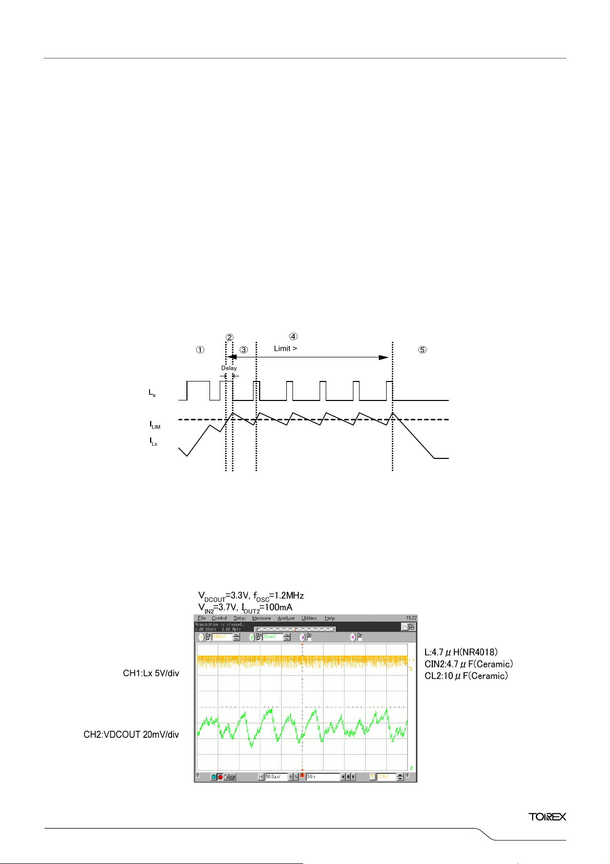
<Current Limit>
The current limiter circuit of the XCM524series monitors the current flowing through the P-channel MOS driver transistor
connected to the Lx pin, and features a combination of the current limit mode and the operation suspension mode.
①When the driver current is greater than a specific level, the current limit function operates to turn off the pulses from the Lx pin
at any given timing.
②When the driver transistor is turned off, the limiter circuit is then released from the current limit detection state.
③At the next pulse, the driver transistor is turned on. However, the transistor is immediately turned off in the case of an over
current state.
④When the over current state is eliminated, the IC resumes its normal operation.
The IC waits for the over current state to end by repeating the steps ①through ③. If an over current state continues for a
few ms and the above three steps are repeatedly performed, the IC performs the function of latching the OFF state of the
P-channel driver transistor, and goes into operation suspension mode. Once the IC is in suspension mode, operations can be
resumed by either turning the IC off via the CE/MODE pin, or by restoring power to the V
not mean a complete shutdown, but a state in which pulse output is suspended; therefore, the internal circuitry remains in
operation. The current limit of the XCM524 series can be set at 1050mA at typical. Besides, care must be taken when laying
out the PC Board, in order to prevent miss-operation of the current limit mode. Depending on the state of the PC Board, latch
time may become longer and latch operation may not work. In order to avoid the effect of noise, the board should be laid out
so that input capacitors are placed as close to the IC as possible.
Limit<#ms
Limit<数ms
Limit>#ms
Limit>数ms
ILx
V
DCOUT
Lx
VEN2
VIN2
pin. The suspension mode does
IN2
Current Limit LEVEL
0mA
VSS
Restart
13/52
XCM524 Series
■OPERATIONAL EXPLANATION (Continued)
<Short-Circuit Protection>
The short-circuit protection circuit monitors the internal R1 and R2 divider voltage from the DCOUT pin. In case where
output is accidentally shorted to the Ground and when the FB point voltage decreases less than half of the reference
voltage (Vref) and a current more than the I
turn off and to latch the P-channel MOS driver transistor. In latch state, the operation can be resumed by either turning the
IC off and on via the EN2 pin, or by restoring power supply to the V
When sharp load transient happens, a voltage drop at the DCOUT pin is propagated to FB point through C
circuit protection may operate in the voltage higher than 1/2 V
<UVLO Circuit>
When the V
IN2 pin voltage becomes 1.4V or lower, the P-channel output driver transistor is forced OFF to prevent false pulse
output caused by unstable operation of the internal circuitry. When the V
operation takes place. By releasing the UVLO function, the IC performs the soft start function to initiate output startup
operation. The soft start function operates even when the VIN pin voltage falls momentarily below the UVLO operating voltage.
The UVLO circuit does not cause a complete shutdown of the IC, but causes pulse output to be suspended; therefore, the
internal circuitry remains in operation.
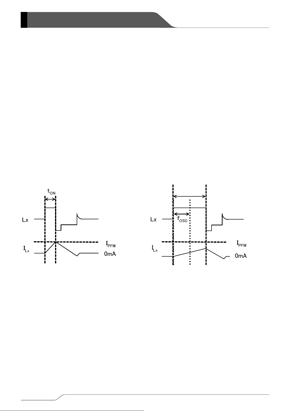
<PFM Switch Current>
In the PFM control operation, until coil current reaches to a specified level (I
case, on-time (t
t
= L×I
ON
PFM
) that the P-ch MOSFET is kept on can be given by the following formula.
ON
/(V
IN2-VDCOUT
) →I
PFM
①
<PFM duty Limit>
In the PFM control operation, the PFM duty limit (DTY
duty increases (e.g. the condition that the step-down ratio is small), it’s possible for P-ch MOSFET to be turned off even when
coil current doesn’t reach to I
PFM
. →I
PFM
①
14/52
flows to the driver transistor, the short-circuit protection quickly operates to
LIM
pin.
IN2
voltage.
OUT
pin voltage becomes 1.8V or higher, switching
IN2
) , the IC keeps the P-ch MOSFET on. In this
PFM
) is set to 200% (TYP.). Therefore, under the condition that the
PFM Duty Limit
I
② I
PFM
PFM
LIMIT_PFM
②
, as a result, short
FB

X
CM524
Series
■OPERATIONAL EXPLANATION (Continued)
High Speed Discharge>
<C
L
XCM524 series can quickly discharge the electric charge at the output capacitor (CL2) when a low signal to the CE pin which
enables a whole IC circuit put into OFF state, is inputted via the N-channel MOS switch located between the L
pin. When the IC is disabled, electric charge at the output capacitor (C
malfunction. Discharge time of the output capacitor (C
) is set by the CL auto-discharge resistance (R) and the output capacitor
L
) is quickly discharged so that it may avoid application
L
(CL). By setting time constant of a CL auto-discharge resistance value [R] and an output capacitor value (CL2) as
τ(τ=C x R), discharge time of the output voltage after discharge via the N channel transistor is calculated by the following
formula.
-t /
V = V
DCOUT(T)
τ
×e
or t = τLn ( V
DCOUT(T)
/V)
V : Output voltage after discharge,
V
: Output voltage after discharge
DCOUT(T)
t: Discharge time
τ: C×R
C = Capacitance of Output capacitor(C
auto-discharge resistance
R = C
L
)
L2
pin and the VSS
X
100
)
e
u
l
a
V
e
v
i
t
a
l
e
R
(
e
g
a
t
l
o
V
t
u
p
t
u
O
90
e
80
u
l
a
V
70
e
g
60
a
t
l
o
50
V
g
n
i
40
t
t
e
30
S
=
20
0
0
1
10
0
0 102030405060708090100
CL=10uF
CL=20uF
CL=50uF
■NOTE ON USE
When the DC/DC converter and the VR are connected as V
DCOUT=VIN1
1. When larger value is used in DC/DC output capacitor CL2, the larger value is also used in C
noted that when C
capacitance of the VR is getting large, an inrush current increases at VR start-up, DC/DC short circuit
L2
protection starts to operate, as a result, the IC may happen to stop.
DCOUT(1V/div)
IIN2(500mA/div)
VROUT(1V/div)
short-circuit protection to start
短絡保護動作
EN2(5V/div)
50us/div
* VR inrush current I
start, as a result, the IC may happen to stop.
The left waver forms are taken at C
contrast to the recommended 1.0μF).
, the following points should be noted.
makes DC/DC short-circuit protection to
IN1
as in proportional. Please be
L1
=10μ, CL2=10μF(in
L1
15/52

XCM524 Series
■NOTE ON USE (Continued)
<VDR BLOCK>
1. Please use this IC within the stated absolute maximum ratings. The IC is liable to malfunction should the ratings be
exceeded.
2. Where wiring impedance is high, operations may become unstable due to noise and/or phase lag depending on output
current. Especially, V
3. Please wire the input capacitor (C
Care shall be taken for capacitor selection to ensure stability of phase compensation from the point of ESR influence.
<DC/DC BLOCK>
1. The XCM524 series is designed for use with ceramic output capacitors. If, however, the potential difference is too large
between the input voltage and the output voltage, a ceramic capacitor may fail to absorb the resulting high switching
energy and oscillation could occur on the output. If the input-output potential difference is large, connect an electrolytic
capacitor in parallel to compensate for insufficient capacitance.
2. Spike noise and ripple voltage arise in a switching regulator as with a DC/DC converter. These are greatly influenced by
external component selection, such as the coil inductance, capacitance values, and board layout of external components.
Once the design has been completed, verification with actual components should be done.
3. As a result of input-output voltage and load conditions, oscillation frequency goes to 1/2, 1/3, and continues, then a ripple
may increase.
4. When input-output voltage differential is large and light load conditions, a small duty cycle comes out. After that, 0%duty
cycle may continue in several periods.
5. When input-output voltage differential is small and heavy load conditions, a large duty cycle comes out and may
continues100% duty cycle in several periods.
6. With the IC, the peak current of the coil is controlled by the current limit circuit. Since the peak current increases when
dropout voltage or load current is high, current limit starts operation, and this can lead to instability. When peak current
becomes high, please adjust the coil inductance value and fully check the circuit operation. In addition, please calculate
the peak current according to the following formula:
Ipk =(V
L:Coil Inductance Value
f
7. When the peak current which exceeds limit current flows within the specified time, the built-in P-channel MOS driver
transistor turns off. During the time until it detects limit current and before the P-channel built-in transistor can be turned
off, the current for limit current flows; therefore, care must be taken when selecting the rating for the external components
such as a coil.
8. Depending on the state of the PC Board, latch time may become longer and latch operation may not work. In order to avoid
the effect of noise, the board should be laid out so that input capacitors are placed as close to the IC as possible.
9. Use of the IC at voltages below the recommended voltage range may lead to instability.
10. This IC should be used within the stated absolute maximum ratings in order to prevent damage to the device.
11. When the IC is used in high temperature, output voltage may increase up to input voltage level at no load because of the
leak current of the P-channel MOS driver transistor.
IN2-VDCOUT
:Oscillation Frequency
OSC
and VSS wiring should be taken into consideration for reinforcement.
IN1
) and the output capacitor (CL1) as close to the IC as possible.
IN1
)×OnDuty/(2×L×f
OSC
) + I
OUT2
16/52
X
CM524
Series
■NOTE ON USE (Continued)
12. The current limit is set to 1350mA (MAX.)
In case that the current limit functions while the DCOUT pin is shorted to the GND pin, when P-channel MOSFET is ON,
the potential difference for input voltage will occur at both ends of a coil. For this, the time rate of coil current becomes
large. By contrast, when N- channel MOSFET switch is ON, there is almost no potential difference at both ends of the coil
since the DCOUT pin is shorted to the GND pin. Consequently, the time rate of coil current becomes quite small.
According to the repetition of this operation, and the delay time of the circuit, coil current will be converged on a certain
current value, exceeding the amount of current, which is supposed to be limited originally. Even in this case, however,
after the over current state continues for several ms, the circuit will be latched. A coil should be used within the stated
absolute maximum rating in order to prevent damage to the device.
①Current flows into P-channel MOS driver transistor to reach the current limit (I
②The current of I
OFF of P-channel MOS driver transistor.
③Because of no potential difference at both ends of the coil, the time rate of coil current becomes quite small.
④Lx oscillates very narrow pulses by the current limit for several ms.
⑤The circuit is latched, stopping its operation.
or more flows since the delay time of the circuit occurs during from the detection of the current limit to
LIM
at typical. However, the current of 1350mA or more may flow.
).
LIM
# ms
13. In order to stabilize V
connected as close as possible to the V
14. High step-down ratio and very light load may lead an intermittent oscillation.
15. During PWM / PFM automatic switching mode, operating may become unstable at transition to continuous mode.
Please verify with actual parts.
’s voltage level and oscillation frequency, we recommend that a by-pass capacitor (CIN2) be
IN1
IN2 & VSS pins.
<External Components>
17/52
XCM524 Series
■NOTE ON USE (Continued)
16. Please note the L value of the coil. The IC may enter unstable operation if the combination of ambient temperature, setting
voltage, oscillation frequency, and L value are not adequate.
The Range of L Value
<External Components>
17. Under input-output voltage differential is large, operating may become unstable at transition to continuous mode.
Please verify with actual parts.
●
f
V
OSC
3.0MHz
1.2MHz
*When a coil less value of 4.7μH is used at when a coil
less value of 1.5μH is used at f
current more easily reach the current limit ILMI. In this
case, it may happen that the IC can not provide 600mA
output current.
0.8V≦V
V
DCOUT
2.5V<V
L Value
DCOUT
≦4.0V 1.0μH〜2.2μH
DCOUT
≦2.5V 3.3μH〜6.8μH
4.7μH〜6.8μH
DCOUT
=3.0MHz, peak coil
OSC
<External Components>
●Instructions of pattern layouts
1. Please use this IC within the stated absolute maximum ratings. The IC is liable to malfunction should the ratings be
exceeded.
2. In order to stabilize V
C
) be connected as close as possible to the V
L2
IN1・VIN2
・DCOUT・V
3. Please mount each external component as close to the IC as possible.
4. Wire external components as close to the IC as possible and use thick, short connecting traces to reduce the circuit
impedance.
5. V
(AGND・PGND・VSS)ground wiring is recommended to get large area. The IC may goes into unstable operation as
SS
a result of V
voltage level fluctuation during the switching.
SS
6. This series’ internal driver transistors bring on heat because of the output current (I
transistors.
●Recommended Pattern Layout
voltage level, we recommend that a by-pass capacitor (C
ROUT
IN1・VIN2
・DCOUT・V
and GND・V
ROUT
pins.
SS
) and ON resistance of driver
OUT
IN1・CIN2・CL1
・
Front Back
18/52

X
■
TEST CIRCUITS
Outpur Capacitor
V
ROUT
CL
CM524
Series
0.9 ~1.2V 1.3 ~ 1.7V 1.8V ~ 5.1V
≧4.7μF ≧2.2μF ≧1.0μF
19/52

XCM524 Series
■TEST CIRCUITS (Continued)
20/52

X
■
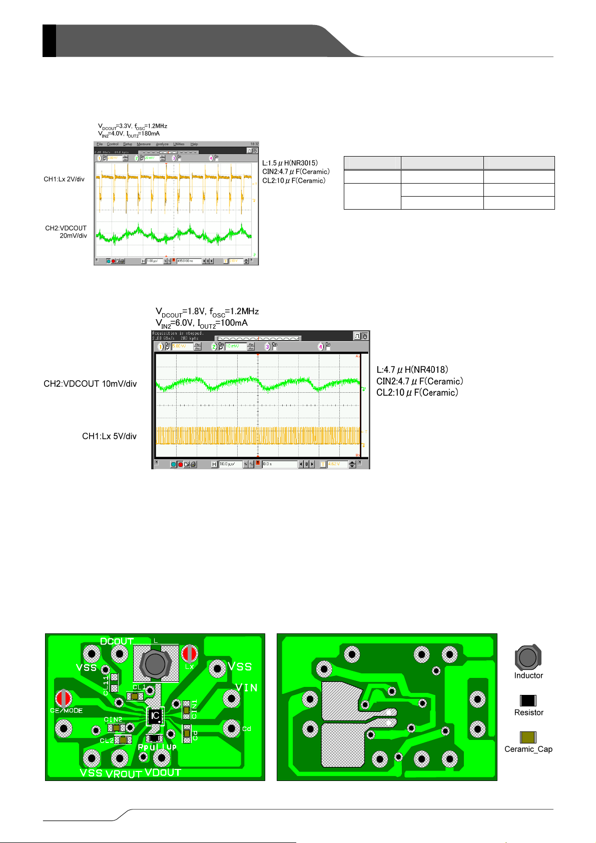
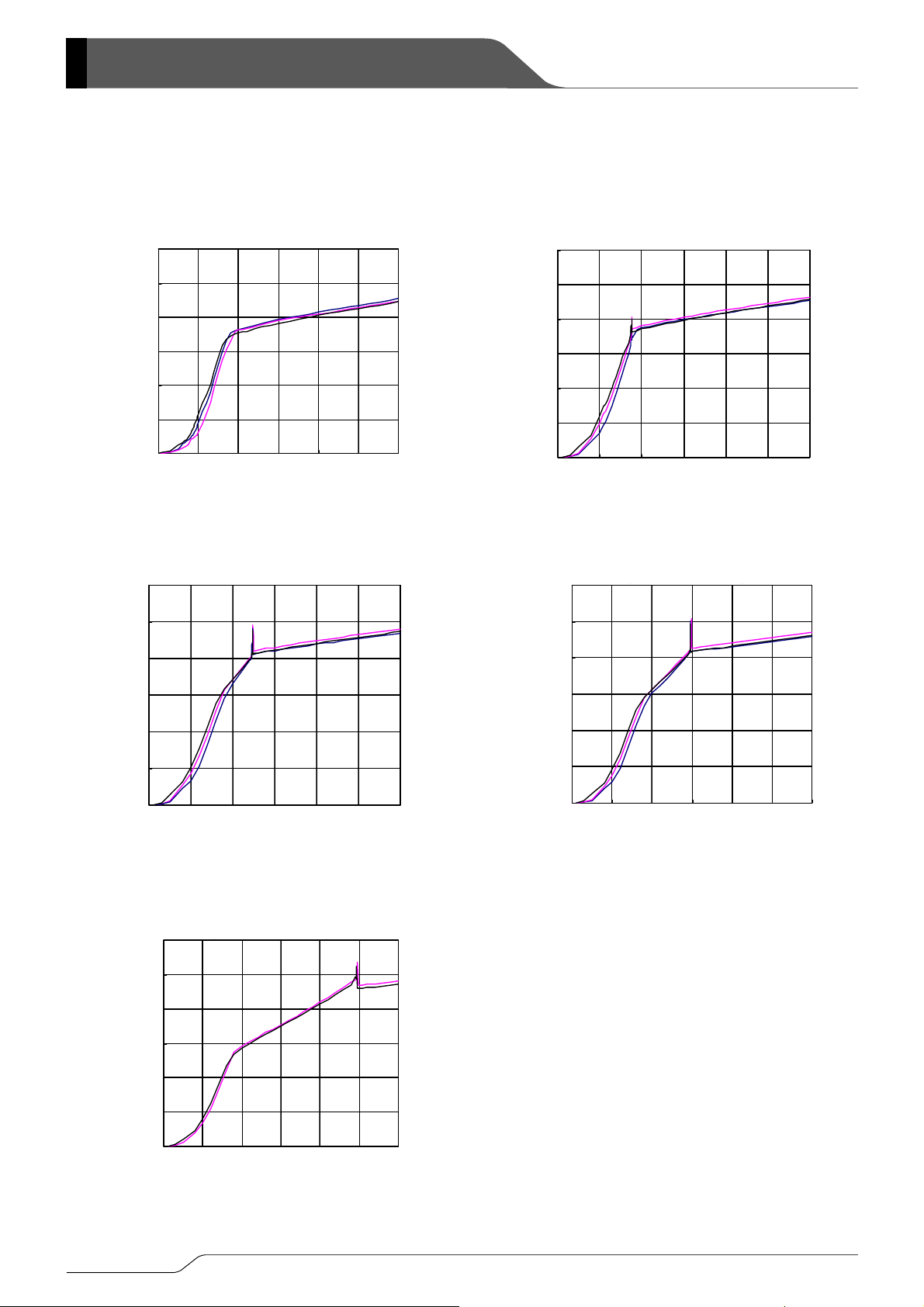
TYPICAL PERFORMANCE CHARACTERISTICS
CM524
Series
●1ch:VDR Block
(1)VR Output Voltage vs. VR Output Current
)
V
(
(V)
ROUT
Output Voltage VRO UT
Output Voltage: V
2.5
2.0
1.5
1.0
0.5
0.0
XC6405 Series (V R:1.8V) XC6405 Series (V R:1.8V)
V
=1.8V
ROUT
CIN=1.0μF (ceramic), CL=1.0μF (c eramic )
C
=1.0μF(ceramic), CL1=1.0μF(ceramic)
IN1
Topr= 25
Top r = - 40
Topr= 85
℃
℃
℃
0 100 200 300 400 500 600 700
Output Current IROUT(mA)
3.0
Output Current: I
XC6405 Series (V R:2.5V)
V
ROUT
CIN=1.0μF (ceramic), CL=1.0μF (cer a mic)
C
=1.0μF(ceramic), CL1=1.0μF(ceramic)
IN1
ROUT
=2.5V
(mA)
VIN=3.8V,
V
=3.8V
IN1
V
=4.5V
VIN=4.5V,
IN1
V
=1.8V
ROUT
CIN=1 .0μF (ceramic), CL=1.0μF (c eramic )
C
=1.0μF(ceramic), CL1=1.0μF(ceramic)
IN1
)
V
(
(V)
ROUT
2.5
2.0
1.5
1.0
0.5
Output Voltage VROUT
Output Voltage: V
0.0
0 100 200 300 400 500 600 700
Output Current IROUT(mA )
3.0
Output Current: I
V
XC6405 Series ( VR:2.5V )
CIN=1.0μF (ceramic), CL=1.0μF (cer a mic )
C
IN1
ROUT
=1.0μF(ceramic), CL1=1.0μF(ceramic)
ROUT
=2.5V
(mA)
VIN= 3.8V
VIN= 2.1V
VIN= 6.0V
2.5
)
V
(
(V)
ROUT
2.0
1.5
Topr= 25
Topr= - 40
Topr= 85
℃
℃
℃
1.0
Output Voltage VROUT
0.5
Output Voltage: V
0.0
0 100 200 300 400 500 600 700
4.0
Output Current: I
Outp ut Current IROUT(mA)
XC6405 Series (V R:3.0V)
CIN=1.0μF (ceramic), CL=1.0μF (cer a mic)
C
=1.0μF(ceramic), CL1=1.0μF(ceramic)
IN1
V
ROUT
ROUT
=3.0V
3.5
)
V
3.0
(
(V)
ROUT
2.5
2.0
Topr= 25
Top r = - 40
Topr= 85
℃
℃
℃
1.5
1.0
Output Voltage VRO UT
0.5
Output Voltage: V
0.0
0 100 200 300 400 500 600 700
Output Current: I
Output Current IROUT(mA)
ROUT
(mA)
(mA)
VIN=5.0V,
V
=5.0V
IN1
2.5
)
V
(
(V)
2.0
ROUT
1.5
VIN= 4.5V
VIN= 2.8V
VIN= 6.0V
1.0
Output Voltage VROUT
0.5
Output Voltage: V
0.0
0 100 200 300 400 500 600 700
)
V
(
(V)
ROUT
4.0
3.5
3.0
2.5
Output Current: I
Output Current IROUT(mA )
XC6405 Series ( VR:3.0V )
V
ROUT
CIN=1.0μF (ceramic), CL=1.0μF (cer a mic)
C
=1.0μF(ceramic), CL1=1.0μF(ceramic)
IN1
ROUT
=3.0V
(mA)
2.0
1.5
1.0
Output Voltage VROUT
0.5
Output Voltage: V
VIN= 5.0V
VIN= 6.0V
0.0
0 100 200 300 400 500 600 700
Output Current IROUT(mA )
Output Current: I
ROUT
(mA)
21/52

■
XCM524 Series
TYPICAL PERFORMANCE CHARACTERISTICS (Continued)
(1)VR Output Voltage vs. VR Output Current (Continued)
6.0
XC6405 Series ( VR:5.0V )
V
=5.0V
ROUT
VIN=6.0V,
V
=6.0V
CIN=1.0μF (ceramic), CL=1.0μF (c eramic )
C
=1.0μF(ceramic), CL1=1.0μF(ceramic)
IN1
IN1
CIN=1.0μF (ceramic), CL=1.0μF (cer a mic)
6.0
C
V
XC6405 Series (VR:5.0V )
=1.0μF(ceramic), CL1=1.0μF(ceramic)
IN1
ROUT
=5.0V
5.0
)
V
(
(V)
ROUT
Output Voltage VROUT
4.0
3.0
2.0
1.0
Topr= 25
Topr= - 40
Topr= 85
℃
℃
℃
Output Voltage: V
0.0
0 100 200 300 400 500 600 700
Output Current IROUT(mA)
)
V
(
(V)
ROUT
Output Current: I
XC6405 Series ( VR:0.9V )
CIN=1.0μF (ceramic), CL=4.7μF (cer a mic)
C
=1.0μF(ceramic), CL1=4.7μF(ceramic)
1.5
1.2
0.9
0.6
IN1
Top r = 2 5
Top r = - 4 0
Top r = 8 5
V
ROUT
ROUT
=0.9V
℃
℃
℃
(mA)
VIN=2.9V,
V
=2.9V
)
5.0
V
(
(V)
4.0
ROUT
3.0
2.0
1.0
Output Voltage VRO UT
Output Voltage: V
0.0
0 100 200 300 400 500 600 700
1.5
)
1.2
V
(
(V)
0.9
ROUT
0.6
VIN= 6.0V
Output Current IROUT (mA)
Output Current: I
XC6405 Series (V R:0.9V)
V
ROUT
CIN=1.0μF (ceramic), CL=4.7μF (cer a mic)
C
=1.0μF(ceramic), CL1=4.7μF(ceramic)
IN1
ROUT
=0.9V
(mA)
0.3
Output Voltage VRO UT
Output Voltage: V
0.0
0 100 200 300 400 500 600 700
Output Current IROUT(mA)
Output Current: I
ROUT
(mA)
ROUT
VIN= 2.0V
VIN= 2.9V
VIN= 6.0V
(mA)
0.3
Output Voltage VRO UT
Output Voltage: V
0.0
0 100 200 300 400 500 600 700
Outp ut Current IROUT(mA)
Output Current: I
22/52

X
℃
℃
℃
℃
℃
℃
■
℃
(
(
)
℃
(
(
)
℃
(
(
)
(
(
)
TYPICAL PERFORMANCE CHARACTERISTICS (Continued)
(2)VR Output Voltage vs. Input Voltage
V
ROUT
=0.9V
Topr=25
Ta =2 5 ℃
IOUT =0mA
1mA
30mA
100mA
)
V
(
(V)
ROUT
1.00
CIN=1 .0μF (ceramic), CL=4.7μF (c er a mic )
=1.0μF(ceramic), CL1=4.7μF(ceramic)
C
IN1
)
V
(
(V)
ROUT
1.5
1.3
1.1
XC6405 Ser ie s (VR:0.9V) XC6405 Ser ie s (VR:0.9V)
CIN=1. 0μF (ceramic), CL=4.7μF (ceramic)
C
=1.0μF(ceramic), CL1=4.7μF(ceramic)
IN1
0.80
0.9
V
ROUT
=0.9V
Topr=25
IOUT =0mA
1mA
30mA
100mA
CM524
Series
Ta =2 5 ℃
0.7
Output Voltage VROUT
Output Voltage: V
0.5
0.5 1.0 1.5 2.0 2.5
2.0
)
1.8
V
(
Input Voltage VIN ( V)
Input Voltage: V
XC6405 Ser ie s (VR:1.8V )
V
ROUT
CIN=1 .0μF (c er a mic ) , CL=1. 0μF (cer a mic )
C
=1.0μF
IN1
ceramic), C
IN1
=1.8V
(V)
=1.0μF
L1
(V)
1.6
ROUT
IOUT =0mA
1.4
1.2
Output Voltage VROUT
Output Voltage: V
1.0
1.3 1.8 2.3
Input Voltage VIN ( V)
Input Voltage: V
(V)
IN1
Topr=25
Ta =2 5
ceramic
1mA
30mA
100mA
Output Voltage VROUT
Output Voltage: V
0.60
2.03.04.05.06.0
CIN=1 .0μF (c er a mic ) , CL=1. 0μF (cer a mic )
)
V
(
(V)
ROUT
1.90
1.85
1.80
1.75
Input Voltage VIN ( V)
Input Voltage: V
V
=1.0μF
IN1
ROUT
ceramic), C
XC6405 Ser ie s (VR:1.8V)
C
=1.8V
(V)
IN1
L1
Topr=25
=1.0μF
IOUT =0mA
Ta =2 5
ceramic
1mA
1.70
Output Voltage VROUT
30mA
100mA
Output Voltage: V
1.65
3.0 3.5 4.0 4.5 5.0 5.5 6.0
Input Voltage VIN (V )
Input Voltage: V
(V)
IN1
V
=2.5V
ROUT
XC6405 Ser ie s (VR:2.5V)
CIN=1 .0μF (ceramic), CL=1.0μF (ceramic)
C
=1.0μF
IN1
ceramic), C
=1.0μF
L1
Topr=25
Ta =2 5
ceramic
)
V
(
(V)
ROUT
2.7
2.5
2.3
XC6405 Ser ie s (VR:2.5V )
V
=2.5V
ROUT
CIN=1 .0μF (ceramic), CL=1.0μF (ceramic)
C
=1.0μF
IN1
ceramic), C
=1.0μF
L1
Top r =25
Ta =2 5 ℃
ceramic
2.60
)
V
2.55
(
(V)
ROUT
2.50
IOUT =0mA
2.1
1.9
Output Voltage VROUT
Output Voltage: V
1.7
2.0 2.5 3.0
Input Voltage VIN (V )
Input Voltage: V
IN1
(V)
1mA
30mA
100mA
IOUT =0mA
2.45
Output Voltage VROUT
Output Voltage: V
2.40
3.0 3.5 4.0 4.5 5.0 5.5 6.0
Input Voltage VIN (V )
Input Voltage: V
(V)
IN1
1mA
30mA
100mA
23/52

)
)
■
℃
(
(
)
℃
(
(
)
℃
(
(
)
XCM524 Series
TYPICAL PERFORMANCE CHARACTERISTICS (Continued)
(2)VR Output Voltage vs. Input Voltage (Continued)
V
=3.0V
ROUT
3.2
XC6405 Series (V R:3.0V)
CIN=1.0μF (ceramic), CL=1.0μF (c eramic )
C
=1.0μF
IN1
ceramic), C
=1.0μF
L1
Top r =25
Ta =2 5
ceramic
℃
3.10
XC6405 Series (V R:3.0V)
V
CIN=1.0μF (ceramic), CL=1.0μF (c eramic )
C
=1.0μF
IN1
=3.0V
ROUT
ceramic), C
=1.0μF
L1
Top r =25
Ta =2 5
ceramic
℃
3.0
(V)
2.8
ROUT
IOUT= 0mA
2.6
2.4
Output Voltage VROUT (V
Output Voltage: V
2.2
2.5 3.0 3.5
Input Voltage VIN (V)
Input Voltage: V
V
XC6405 Series ( VR:5.0V )
CIN=1.0μF (ceramic), CL=1.0μF (c eramic )
C
=1.0μF(ceramic), CL1=1.0μF(ceramic)
5.2
IN1
ROUT
IN1
=5.0V
(V)
5.0
(V)
4.8
ROUT
IOUT= 0mA
4.6
4.4
Output Voltage VROUT (V
Output Voltage: V
4.2
4.5 5.0 5.5
Input Voltage: V
Input Voltage VIN (V)
IN1
(V)
1mA
30mA
100mA
Top r =25
Ta =2 5 ℃
1mA
30mA
100mA
)
3.05
V
(
(V)
3.00
ROUT
2.95
2.90
Output Voltage VRO UT
IOUT =0mA
1mA
30mA
100mA
Output Voltage: V
2.85
4.0 4.5 5.0 5.5 6.0
℃
5.10
)
5.05
V
(
Input Voltage VIN (V)
Input Voltage: V
V
ROUT
XC6405 Series (V R:5.0V)
CIN=1 .0μF (ceramic), CL=1.0μF (c eramic )
C
=1.0μF
IN1
ceramic), C
IN1
=5.0V
(V)
=1.0μF
L1
Topr=25
Ta =2 5
ceramic
℃
(V)
5.00
ROUT
4.95
4.90
Output Voltage VROUT
IOUT= 0mA
1mA
30mA
100mA
Output Voltage: V
4.85
5.25.3 5.45.55.65.7 5.85.96.0
Input Voltage: V
Input Voltage VIN (V)
IN1
(V)
24/52

X
■
TYPICAL PERFORMANCE CHARACTERISTICS (Continued)
(3)Dropout Voltage vs. VR Output Current
XC6405 Series (V R:0.9V)
V
=0.9V
ROUT
CIN=1.0μF (ceramic), CL=4.7μF (cer a mic )
C
=1.0μF(ceramic), CL1=4.7μF(ceramic)
1.6
IN1
1
XC6405 Series (VR:1.8V )
V
ROUT
CIN=1.0μF (ceramic), CL=1.0μF (cer a mic )
C
=1.0μF(ceramic), CL1=1.0μF(ceramic)
IN1
CM524
Series
=1.8V
1.4
1.2
1
0.8
Dropout Voltage Vdif ( V)
Dropout voltage: Vdif (V)
0.6
0 50 100 150 200
1
0.8
)
V
(
0.6
0.4
Topr= 85
Output Current: I
VR Output Current IROUT (mA)
XC6405 Series (V R:2.5V) XC6405 Series (V R:3.0V)
CIN=1.0μF (ceramic), CL=1.0μF (cer a mic )
C
=1.0μF(ceramic), CL1=1.0μF(ceramic)
IN1
Top r = 8 5
V
25
- 40
ROUT
25
- 40
℃
℃
℃
ROUT
=2.5V
℃
℃
℃
(mA)
0.8
0.6
0.4
0.2
Dropout Voltage Vdif ( V)
Dropout voltage: Vdif (V)
0
0 50 100 150 200
1
0.8
0.6
0.4
Topr= 85
VR Output Current IROUT (mA)
Output Current: I
CIN=1.0μF (ceramic), CL=1.0μF (cer a mic)
C
=1.0μF(ceramic), CL1=1.0μF(ceramic)
IN1
Topr= 85
- 40
-40℃
V
25
- 40
25
ROUT
℃
℃
℃
℃
℃
℃
ROUT
=3.0V
(mA)
Dropout Voltage Vdif
Dropout voltage: Vdif (V)
0.2
0
0 50 100 150 200
Output Current: I
VR Output Current IROUT (mA)
XC6405 Series (V R:5.0V)
V
ROUT
CIN=1.0μF (ceramic), CL=1.0μF (c eramic )
C
=1.0μF(ceramic), CL1=1.0μF(ceramic)
1
0.8
0.6
0.4
Dropout Voltage Vdif ( V)
0.2
Dropout voltage: Vdif (V)
0
0 50 100 150 200
IN1
Topr= 85
25
- 40
VR Output Current IROUT (mA)
Output Current: I
=5.0V
℃
℃
℃
ROUT
ROUT
(mA)
(mA)
Dropout Voltage Vdif ( V)
0.2
Dropout voltage: Vdif (V)
0
0 50 100 150 200
Output Current: I
VR Output Current IROUT (mA)
ROUT
(mA)
25/52
■
XCM524 Series
TYPICAL PERFORMANCE CHARACTERISTICS (Continued)
(4)Supply Current vs. Input Voltage
V
=0.9V
ROUT
XC6405 Series (VR:0.9) XC6403 Serie s (VR:1.8V)
CIN=1.0μF (ceramic), CL=4.7μF (c eramic )
C
=1.0μF(ceramic), CL1=4.7μF(ceramic)
120
IN1
120
CIN=1.0μF (ceramic), CL=1.0μF (cer a mic)
C
IN1
V
=1.0μF(ceramic), CL1=1.0μF(ceramic)
ROUT
=1.8V
100
)
A
(μ
(μA)
80
DD
60
V
ROUT
Topr= 85
- 40
IN1
=2.5V
Topr= 85
40
Supply Cur rent ISS
20
Supply Current: I
0
0.0 1.0 2.0 3.0 4.0 5.0 6.0
Input Voltage: V
Input Voltage VIN (V)
XC6405 Series ( VR:2.5V ) XC6405 Ser ie s (V R:3.0V)
C
=1.0μF(ceramic), CL1=1.0μF(ceramic)
CIN=1 .0μF (ceramic), CL=1.0μF (c eramic )
120
100
)
A
(μA)
80
(μ
DD
60
40
消費電流 Iss (μA)
Supply Current: I
Supply Cur rent ISS
20
IN1
25
(V)
- 40
25
100
)
A
(μ
80
(μA)
DD
60
℃
℃
℃
℃
℃
℃
40
Supply Current ISS
20
Supply Current: I
0
0.0 1.0 2.0 3.0 4.0 5.0 6.0
120
100
A)
μ
80
(μA)
DD
60
40
Supply Current ISS (
Supply Current: I
20
Input Voltage VIN (V)
Input Voltage: V
CIN=1.0μF (ceramic), CL=1.0μF (cer a mic )
C
=1.0μF(ceramic), CL1=1.0μF(ceramic)
IN1
V
ROUT
Topr= 85
IN1
=3.0V
25
- 40
(V)
Topr= 85
℃
℃
℃
℃
25
℃
- 40
℃
0
0.0 1.0 2.0 3.0 4.0 5.0 6.0
Input Voltage: V
Input Voltage VIN (V)
XC6405 Series (V R:5.0V)
V
ROUT
CIN=1.0μF (ceramic), CL=1.0μF (c eramic )
C
=1.0μF(ceramic), CL1=1.0μF(ceramic)
120
100
A)
μ
(μA)
80
DD
60
40
Supply Cur rent ISS (
Supply Current: I
20
0
IN1
0.0 1.0 2.0 3.0 4.0 5.0 6.0
Input Voltage VIN (V)
Input Voltage: V
IN1
=5.0V
IN1
(V)
Topr= 85
25
- 40
(V)
0
0.0 1.0 2.0 3.0 4.0 5.0 6.0
Input Voltage: V
Input Voltage VIN (V)
℃
℃
℃
(V)
IN1
26/52
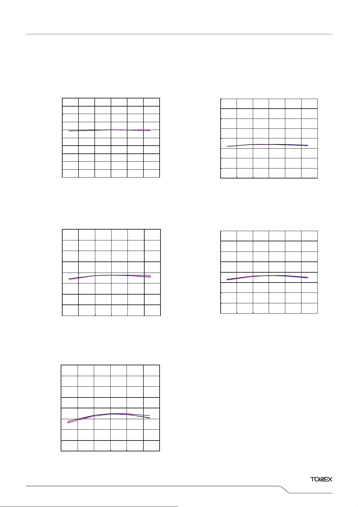
X
■
A
A
A
A
A
TYPICAL PERFORMANCE CHARACTERISTICS (Continued)
(5)VR Output Voltage vs. Ambient Temperature
V
=0.9V
XC6405 Series (V R:0.9)
C
=1.0μF(ceramic), CL1=4.7μF(ceramic)
IN1
CIN=1.0μF (ceramic), CL=4.7μF (cer a mic)
-50-25 0 255075100
Operating Temperature Topr (℃)
mbient Temperature: Ta (℃)
)
V
(
(V)
ROUT
Output Voltage VRO UT
Output Voltage: V
1.10
1.00
0.90
0.80
0.70
0.60
ROUT
VIN=2.0V
V
IOUT =0mA
=30mA
=100mA
IN1
=2.0V
2.00
1.95
)
V
(
1.90
(V)
1.85
ROUT
1.80
1.75
1.70
Output Voltage VROUT
Output Voltage: V
1.65
1.60
-50 -25 0 25 50 75 100
XC6403 Series (VR:1.8V )
C
=1.0μF(ceramic), CL1=1.0μF(ceramic)
IN1
CIN=1.0μF(ceramic), CL=1.0μF (c eramic )
Operating Temperature Topr (℃)
mbient Temperature: Ta (℃)
V
ROUT
=1.8V
VIN=2.8V
V
IOUT =0mA
=30mA
=100mA
IN1
CM524
Series
=2.8V
XC6405 Series ( VR:2.5V )
C
IN1
CIN=1 .0μF (ceramic), CL=1.0μF (c eramic )
-50 -25 0 25 50 75 100
)
V
(
(V)
ROUT
Output Voltage VRO UT
Output Voltage: V
2.70
2.65
2.60
2.55
2.50
2.45
2.40
2.35
2.30
mbient Temperature: Ta (℃)
XC6405 Series ( VR:5.0V )
C
IN1
CIN=1.0μF (ceramic), CL=1.0μF (c eramic )
)
V
(
(V)
ROUT
5.20
5.15
5.10
5.05
5.00
V
=2.5V
ROUT
=1.0μF(ceramic), CL1=1.0μF(ceramic)
IOUT= 0mA
=30mA
=100mA
Operating Temperature Topr (℃)
V
=5.0V
ROUT
=1.0μF(ceramic), CL1=1.0μF(ceramic)
IOUT =0mA
=30mA
=100mA
VIN=3.5V
V
=3.5V
IN1
VIN=6.0V
V
=6.0V
IN1
XC6405 Series (VR:3.0V )
V
=3.0V
ROUT
C
=1.0μF(ceramic), CL1=1.0μF(ceramic)
CIN=1.0μF (ceramic), CL=1.0μF (cer a mic)
3.20
3.15
)
V
3.10
(
(V)
3.05
ROUT
3.00
2.95
2.90
Output Voltage VROUT
Output Voltage: V
2.85
2.80
-50 -25 0 25 50 75 100
IN1
IOUT= 0mA
=100mA
Operating Temperature Topr (℃)
mbient Temperature: Ta (℃)
VIN=4.0V
V
=30mA
IN1
=4.0V
4.95
4.90
Output Voltage VRO UT
Output Voltage: V
4.85
4.80
-50-25 0 25 50 75100
Operating Temperature Topr (℃)
mbient Temperature: Ta (℃)
27/52

■
pp
y
DD
(
μ
)
A
pp
y
(
μ
)
A
A
A
A
XCM524 Series
TYPICAL PERFORMANCE CHARACTERISTICS (Continued)
(6)Supply Current vs. Ambient Temperature
V
=0.9V
ROUT
V
=2.0V
IN1
V
ROUT
=1.8V
V
=2.8V
IN1
A
Current: I
l
Su
(μA)
DD
mbient Temperature: Ta (℃)
V
=2.5V
ROUT
A
DD
Current: I
l
Su
mbient Temperature: Ta (℃)
V
=3.0V
ROUT
V
=3.5V
IN1
(μA)
DD
V
=4.0V
IN1
Supply Current: I
mbient Temperature: Ta (℃)
(μA)
DD
Supply Current: I
mbient Temperature: Ta (℃)
V
ROUT
=5.0V
Supply Current: I
mbient Temperature: Ta (℃)
V
=6.0V
IN1
28/52
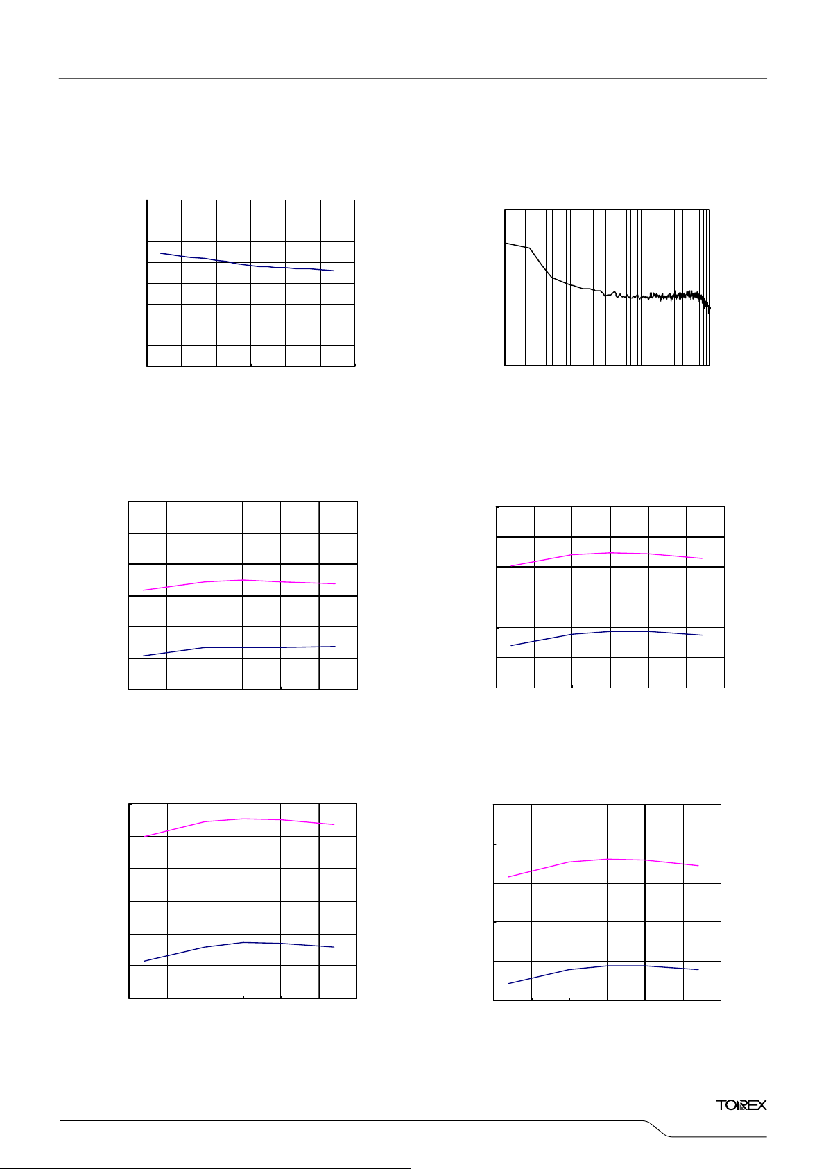
X
■
)
TYPICAL PERFORMANCE CHARACTERISTICS (Continued)
(7)Rdelay vs. Ambient Temperature (8)Output Noise Density
C
=1.0μF(セラミック), CL1=1.0μF(ceramic)
800
700
600
500
400
300
Rdelay (kΩ)
200
100
0
-50 -25 0 25 50 75 100
Ambient Temperature: Ta(℃)
Output Noise Density (μV/RootHz)
10
1
0.1
0.01
IN1
0.1 1 10 100
Frequency: (kHz)
(9)Detect Voltage, Release Voltage vs. Ambient Temperature
2.20
(V)
DR
,V
2.15
DF
2.10
2.05
VDF=2.0V
XC6405 Series (V D:2.0V)
VDR
)
V
(
(V)
DR
,V
DF
2.90
2.85
2.80
2.75
XC6405 Series (V D:2.7V)
VDF=2.7V
V
=4.0V
VIN=4.0V
IOUT=10mA CL=10uF(セラミック
VDR
IN1
CM524
Series
2.00
1.95
1.90
Detect Voltage, Release Voltage VDF,VDR (V)
-50 -25 0 25 50 75 100
Detect Voltage, Release Voltage: V
Operating Temper ature Topr (OC)
Operating Temper ature Topr (℃)
Ambient Temperature: Ta (℃)
VDF
VDF=3.6V
)
3.80
V
(
(V)
DR
3.75
,V
DF
3.70
3.65
3.60
3.55
3.50
Detect Voltage, Release Voltage VDF,VDR
-50 -25 0 25 50 75 100
Detect Voltage, Release Voltage: V
Ambient Temperature: Ta (℃)
Operating Temper ature Topr (℃)
VDR
VDF
2.70
2.65
2.60
Detect Voltage, Release Voltage VDF,VDR
-50 -25 0 25 50 75 100
Detect Voltage, Release Voltage: V
)
5.40
V
(
(V)
DR
,V
5.30
DF
5.20
5.10
5.00
4.90
Detect Voltage, Release Voltage VDF,VDR
-50-25 0 25 50 75100
Detect Voltage, Release Voltage: V
Operating Temperature Topr (℃)
Ambient Temperature: Ta (℃)
XC6405 Series (V D:5.0V)XC6405 Series (V D:3.6V)
Ambient Temperature: Ta (℃)
Operating Temperature Topr (℃)
VDF
VDF=5.0V
VDR
VDF
29/52
℃
℃
℃
■
XCM524 Series
TYPICAL PERFORMANCE CHARACTERISTICS (Continued)
(10)VD N-channel Driver Transistor Output Current vs. VDS
VDF=2.0V
XC6405 Series (VD:2.0V) XC6405 Ser ie s (V D:2.7V)
Ta =2 5 ℃
8
7
)
6
mA
(mA)
(
5
DOUT
4
3
2
Output Current IOUT
Output Current: I
1
0
00.511.522.5
VDS (V)
VDS (V)
Topr =25
VIN=2.0V
16
14
)
12
mA
(mA)
(
10
DOUT
8
6
4
Output Current IOUT
Output Current: I
2
0
00.511.522.53
VDF=2.7V
VIN=1.0V
VDS (V)
VDS (V)
Ta =2 5 ℃
VIN=2.5V
VIN=2.0V
VIN=1.5V
VDF=3.6V
Ta =2 5 ℃
24
21
)
18
mA
(mA)
(
15
DOUT
12
9
VIN=1.5V
VDS (V)
VDS (V)
VIN=2.0V
6
Output Current IOUT
Output Current: I
3
0
01234
Topr =25
VIN=3.0V
VIN=2.5V
XC6405 Series (V D:5.0V)XC6405 Series (V D:3.6V)
VDF=5.0V
Ta =2 5 ℃
32
28
)
24
mA
(mA)
(
20
DOUT
16
12
8
Output Current IOUT
Output Current: I
4
0
01234
VIN=2.0V
VIN=1.5V
VDS (V)
VDS (V)
Topr =25
VIN=4.5V
VIN=3.5V
VIN=2.5V
30/52
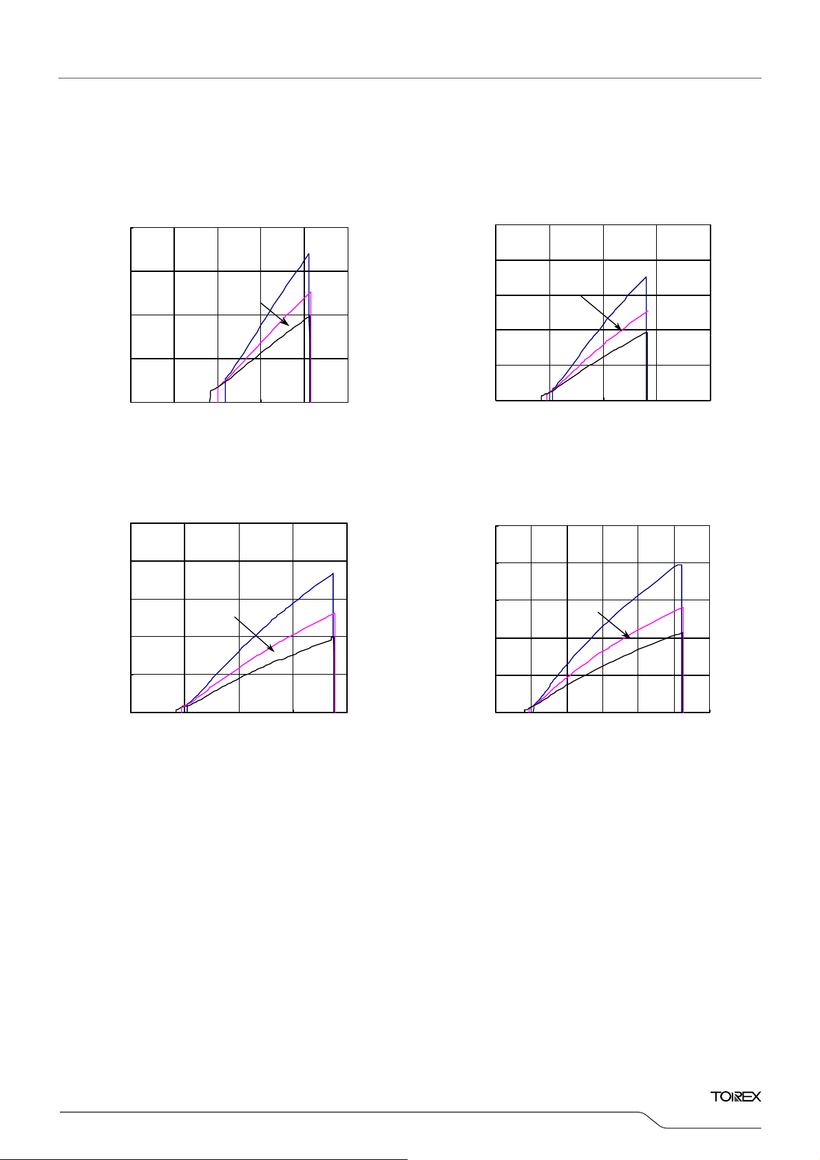
X
℃
℃
℃
■
TYPICAL PERFORMANCE CHARACTERISTICS (Continued)
(11)VD N-channel Driver Transistor Output Current vs. Input Voltage
XC6405 Series ( VD:2.0V )
XC6405 Series (VD:2.7V )
VDF=2.7V VDF=2.0V
CM524
Series
8
)
mA
6
(mA)
(
DOUT
4
2
Output Current IO UT
Output Current: I
0
20
16
)
mA
(mA)
(
DOUT
12
VDS=0.5V
00.511.522.5
Input Voltage VIN (V)
Input Voltage: V
XC6405 Series ( VD:3.6V )
VDF=3.6V VDF=5.0V
VDS=0.5V
25
-40
℃
25
85
℃
(V)
IN1
-40
℃
℃
15
)
12
mA
(mA)
(
DOUT
9
6
3
Output Voltage IO UT
Output Current: I
0
01234
25
)
20
mA
(mA)
(
15
DOUT
VDS=0.5V
-40
℃
25
85
℃
Input Voltage VIN (V)
Input Voltage: V
XC6405 Series (V D:5.0V)
VDS=0.5V
25
℃
IN1
(V)
-40
℃
8
4
Output Current IOUT
Output Current: I
0
01234
Input Voltage VIN (V)
Input Voltage: V
85
(V)
IN1
10
5
Output Current IOUT
Output Current: I
0
01234 56
Input Voltage VIN (V)
Input Voltage: V
85
℃
(V)
IN1
31/52
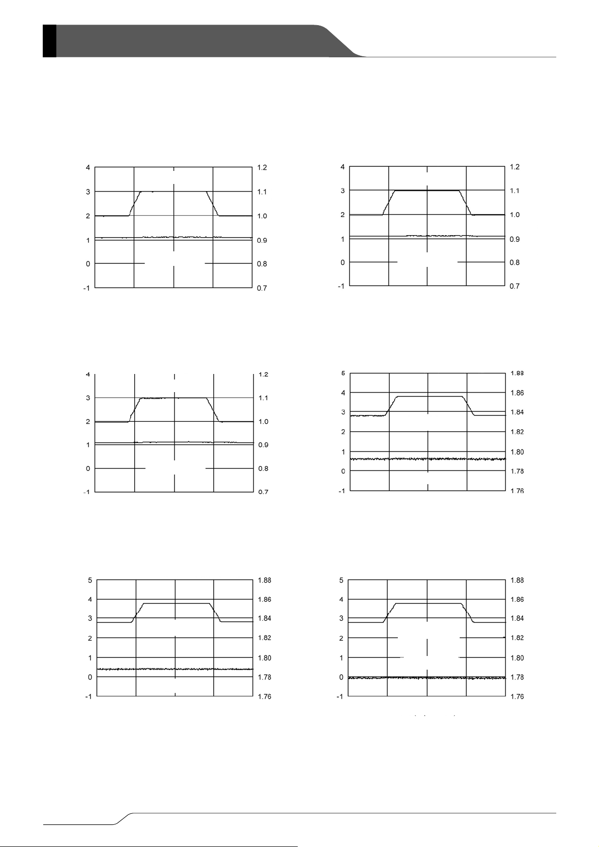
■
入力電圧
入力電圧
入力電圧
(
)
(
)
(
)
(
)
(
)
(
)
XCM524 Series
TYPICAL PERFORMANCE CHARACTERISTICS (Continued)
(12)Input Transient Response
V
=0.9V
ROUT
C
=4.7μF
L1
Input Voltage
I
=1mA, tr=tf=5.0μs
ROUT
ceramic
, Ta=25℃
V
=0.9V
ROUT
I
ROUT
=4.7μF
C
L1
Input Voltage
=30mA, tr=tf=5.0μs
ceramic
, Ta=25℃
(V)
IN1
Input Voltage: V
(V)
IN1
Input Voltage: V
Output Voltage
Time (40μs/div)
V
=0.9V
ROUT
I
=100mA, tr=tf=5.0μs
ROUT
C
=4.7μF
L1
Input Voltage
Output Voltage
ceramic
, Ta=25℃
(V)
ROUT
Output Voltage: V
(V)
ROUT
Output Voltage: V
(V) Input Voltage: V
IN1
Input Voltage: V
(V)
IN1
Output Voltage
Time (40μs /div)
V
=1.8V
ROUT
I
=1mA, tr=tf=5.0μs
ROUT
=1.0μF
C
L1
Input Voltage
Output Voltage
ceramic
(V)
ROUT
Output Voltage: V
, Ta=25℃
(V)
ROUT
Output Voltage: V
(V)
IN1
Input Voltage: V
Time (40μs /div)
V
=1.8V
ROUT
I
=30mA, tr=tf=5.0μs
ROUT
C
=1.0μF
L1
Input Voltage
出力電圧
Output Voltage
Time (40μs /div)
ceramic
, Ta=25℃
(V)
ROUT
出力電圧 VOUT(V)
Output Voltage: V
(V)
IN1
Input Voltage: V
Time (40μs /div)
V
=1.8V
ROUT
I
=100mA, tr=tf=5.0μs
ROUT
C
=1.0μF
L1
Input Voltage
Output Voltage
ceramic
Time (40μs /div)
, Ta=25℃
(V)
ROUT
Output Voltage: V
32/52

X
)
■
入力電圧
(
)
(
)
(
)
(
)
(
)
TYPICAL PERFORMANCE CHARACTERISTICS (Continued)
(12)Input Transient Response (Continued)
V
XC6405 Ser ies (VR:2.5V) XC6405 Ser ie s (V R:2.5V)
6
=2.5V
ROUT
IOUT=1mA, tr=tf=5.0μsec,
I
=1mA, tr=tf=5.0μs
ROUT
CL= 1. 0μF (ceramic), Topr=25
=1.0μF
ceramic
C
L1
, Ta=25℃
℃
2.58
6
V
=2.5V
ROUT
IOUT=30mA, tr =tf=5.0μsec,
CL= 1. 0μF (ceramic), Topr=25
=1.0μF
C
L1
I
=30mA, tr=tf=5.0μs
ROUT
ceramic
, Ta=25℃
CM524
Series
℃
2.58
5
(V)
4
IN1
3
2
Input Voltage VIN (V
Input Voltage: V
1
0
6
5
)
(V)
V
(
4
IN1
3
2
Input Voltage VIN
Input Voltage: V
1
0
Input Voltage
Input Voltage
Output Voltage
Output Voltage
Time (40μs /div)
Time (40μsec/div)
V
XC6405 Series (VR:2.5V )
=2.5V
ROUT
IOUT=100mA, tr=tf=5.0μsec,
I
=100mA, tr=tf=5.0μs
ROUT
CL= 1. 0μF (ceramic), Topr=25
C
=1.0μF
L1
Input Voltage
Input Voltage
Output Voltage
Output Voltage
Time ( 40μsec/div)
Time (40μs /div)
ceramic
℃
, Ta=25℃
2.56
2.54
2.52
2.50
2.48
2.46
2.58
2.56
2.54
2.52
2.50
2.48
2.46
(V)
ROUT
Output Voltage VOUT (V)
Output Voltage: V
)
V
(V)
(
ROUT
出力電圧 VOUT(V) 出力電圧VOUT(V)
Output Voltage VOUT
Output Voltage: V
5
)
(V)
V
(
4
IN1
3
2
Input Voltage VIN
Input Voltage: V
1
0
6
5
)
V
(V)
(
4
IN1
3
2
Input Voltage VIN
Input Voltage: V
1
0
Input Voltage
Input Voltage
Output Voltage
Output Voltage
Time ( 4 0
Time (40μs /div)
V
XC6405 Ser ies (VR:3.0V)
Input Voltage
Output Voltage
Time ( 40μsec/div)
Time (40μs /div)
sec/div)
μ
=3.0V
ROUT
IOUT= 1 mA , tr =tf =5. 0μsec,
I
=1mA, tr=tf=5.0μs
CL= 1.0μF (ceramic), Topr=25
Output Voltage
ROUT
=1.0μF
C
L1
Input Voltage
ceramic
℃
, Ta=25℃
2.56
2.54
2.52
2.50
2.48
2.46
3.08
3.06
3.04
3.02
3.00
2.98
2.96
)
V
(
(V)
ROUT
Output Voltage VOUT
Output Voltage: V
)
V
(
(V)
ROUT
Output Voltage VOUT
Output Voltage: V
V
=3.0V
ROUT
XC6405 Ser ie s (V R:3.0V)
I
=100mA, tr=tf=5.0μs
IOUT=100mA, tr=tf=5.0μsec,
ROUT
=1.0μF(ceramic), Ta=25℃
C
CL= 1.0μF (ceramic), Topr=25
L1
Input Voltage
Input Voltage
Output Voltage
Output Voltage
Time ( 40μsec/div)
Time (40μs /div)
℃
3.08
3.06
)
V
(
(V)
3.04
ROUT
3.02
3.00
Output Voltage VOUT
2.98
Output Voltage: V
2.96
6
5
)
V
(V)
(
4
IN1
3
2
Input Voltage VIN
Input Voltage: V
1
0
V
XC6405 Ser ie s (V R:3.0V)
Input Voltage
=3.0V
ROUT
IOUT=30mA, tr=tf=5.0μsec,
I
=30mA, tr=tf=5.0μs
ROUT
CL= 1.0μF (ceramic), Topr=25
C
=1.0μF
L1
Input Voltage
Output Voltage
Output Voltage
Time ( 40μsec/div)
時間(40μsec/div)
Time (40μs /div)
ceramic
, Ta=25℃
℃
3.08
3.06
)
V
(
(V)
3.04
ROUT
3.02
3.00
Output Voltage VOUT
2.98
Output Voltage: V
2.96
6
5
)
V
(V)
(
4
IN1
3
2
Input Voltage VIN
Input Voltage: V
1
0
33/52

■
(
)
(
)
(
)
XCM524 Series
TYPICAL PERFORMANCE CHARACTERISTICS (Continued)
(12)Input Transient Response (Continued)
V
=5.0V
ROUT
8
7
)
(V)
V
(
IN1
6
5
4
Input Voltage VIN
Input Voltage: V
3
2
XC6405 Ser ies (V R:5.0V)
IOUT=1mA, tr =tf=5.0μsec,
I
=1mA, tr=tf=5.0μs
ROUT
CL= 1. 0μF (cer a mic), To pr =25
=1.0μF
ceramic
C
L1
Inp u t V oltag e
Input Voltage
Output Voltage
Output Voltage
時間(40μsec/div) 時間(40μsec/div)
Time ( 40μsec/div)
Time (40μs /div)
, Ta=25℃
℃
5.08
5.06
5.04
5.02
5.00
4.98
4.96
)
V
(V)
(
ROUT
出力電圧 VOUT(V) 出力電圧 VOUT(V) 出力電圧 VOUT(V)
Output Voltage VOUT
Output Voltage: V
8
7
(V)
6
IN1
5
4
入力電圧 VIN(V)
Input Voltage VIN (V)
Input Voltage: V
3
2
XC6405 Ser ies (V R:5.0V)
V
=5.0V
ROUT
IOUT=30mA, tr =tf=5.0μsec,
I
ROUT
CL= 1. 0μF (cer a mic), To pr =25
=1.0μF
C
L1
Input Voltage
Input Voltage
Output Voltage
Output Voltage
Time (40μs /div)
Time ( 40μsec/div)
=30mA, tr=tf=5.0μs
ceramic
, Ta=25℃
℃
5.08
5.06
)
V
(
5.04
5.02
5.00
4.98
(V)
ROUT
Output Voltage VOUT
Output Voltage: V
4.96
8
7
)
V
(V)
(
6
IN1
5
4
Input Voltage VIN
Input Voltage: V
3
2
V
XC6405 Ser ies (V R:5.0V)
=5.0V
ROUT
IOUT=100mA, tr=tf=5.0μsec,
I
=100mA, tr=tf=5.0μs
ROUT
CL= 1.0μF (ceramic), Topr=25
C
=1.0μF
L1
Input Voltage
Input Voltage
Output Voltage
Output Voltage
Time (40μs/div)
Time ( 40μsec/div)
ceramic
, Ta=25℃
℃
5.08
5.06
5.04
5.02
5.00
4.98
4.96
)
V
(
(V)
ROUT
Output Voltage VOUT
Output Voltage: V
34/52

X
■
(
)
時間
(
(
)
(
)
(
)
(
)
(
)
TYPICAL PERFORMANCE CHARACTERISTICS (Continued)
(13)Load Transient Response
V
=0.9V
ROUT
V
=2.0V, tr=tf=5.0μs, Ta=25℃
C
IN1
IN1
=1.0μF(ceramic), CL1=4.7μF(ceramic)
C
V
ROUT
V
=2.0V, tr=tf=5.0μs, Ta=25℃
IN1
=1.0μF(ceramic), CL1=4.7μF(ceramic)
IN1
CM524
Series
=0.9V
(V)
ROUT
Output Voltage: V
(V)
ROUT
入力電圧 VIN(V)
Output Voltage: V
Output Voltage
Output Current
Time
20μs /div
V
ROUT
V
=2.0V, tr=tf=5.0μsec, Ta=25℃
C
IN1
=1.0μF(ceramic), CL1=4.7μF(ceramic)
IN1
入力電圧
Output Voltage
Output Current
=0.9V
(mA)
ROUT
Output Current: I
(mA)
ROUT
出力電圧 VOUT (V)
Output Current: I
(V)
ROUT
入力電圧 VIN(V)
Output Voltage: V
(V)
ROUT
Output Voltage: V
Output Voltage
Output Current
Time
20μs /div
V
=1.8V
ROUT
V
=2.8V, tr=tf=5.0μs
IN1
=1.0μF(ceramic), Ta=25℃
C
IN1=CL1
Output Voltage
Output Current
(mA)
ROUT
Output Current: I
(mA)
ROUT
Output Current: I
(V)
ROUT
Output Voltage: V
時間(20μsec/div)
40μsec/div)
Time
20μs /div
V
=1.8V
ROUT
V
IN1
=1.0μF(ceramic), Ta=25℃
C
IN1=CL1
Output Voltage
Output Current
Time
20μs /div
=2.8V, tr=tf=5.0μs
(mA)
ROUT
Output Current: I
(V)
ROUT
Output Voltage: V
Time
20μs /div
V
=1.8V
ROUT
V
=2.8V, tr=tf=5.0μs
IN1
=1.0μF(ceramic), Ta=25℃
C
IN1=CL1
Output Voltage
Output Current
Time
20μs /div
(mA)
ROUT
Output Current: I
35/52

■
(
)
(
)
(
)
(
)
(
)
(
)
XCM524 Series
TYPICAL PERFORMANCE CHARACTERISTICS (Continued)
(13)Load Transient Response (Continued)
V
)
V
(V)
(
ROUT
2.55
2.50
2.45
XC6405 Ser ie s (V R:2.5V) XC6405 Ser ie s (V R:2.5V)
C
IN1=CL1
CIN=CL= 1.0μF (ceramic), Topr=25
Output Voltage
V
=3.5V, tr=tf=5.0μs
VIN=2.5V , tr=tf=5.0μsec
IN1
=1.0μF(ceramic), Ta=25℃
Output Voltage
℃
250
)
200
mA
(mA)
(
ROUT
150
2.55
2.50
)
V
(V)
(
ROUT
2.45
=2.5V
ROUT
V
ROUT
=1.0μF(ceramic), Ta=25℃
C
CIN=CL= 1.0μF (ceramic), Topr=25
IN1=CL1
Output Voltage
Output Voltage
=2.5V
V
=3.5V, tr=tf=5.0μs
VIN=2.5V , tr=tf=5.0μsec
IN1
℃
250
200
)
mA
(mA)
(
ROUT
150
Output Voltage VOUT
Output Voltage: V
(V)
ROUT
Outpu t V oltage VO UT (V)
Output Voltage: V
2.40
2.35
2.30
2.55
2.50
2.45
2.40
2.35
2.30
Output Current
Output Current
Time
20μs /div
Time ( 2 0μsec/div)
XC6405 Ser ies (V R:2.5V)
V
=2.5V
ROUT
V
VIN=2.5V, tr=tf =5.0μsec
=1.0μF(ceramic), Ta=25℃
C
IN1=CL1
CIN=CL =1. 0μF (ceramic), Topr=25
Output Voltage
Output Voltage
Output Cur rent
Output Current
Time (20μsec/div)
Time
20μs /div
=3.5V, tr=tf=5.0μs
IN1
100
50
Output Curr ent IOUT
Output Current: I
0
℃
250
200
(mA)
150
ROUT
100
Ou tpu t Cu rre n t I OUT (mA)
50
Output Current: I
0
2.40
Output Voltage VOUT
2.35
Output Voltage: V
2.30
)
V
(V)
(
ROUT
Output Voltage VOUT
Output Voltage: V
3.05
3.00
2.95
2.90
2.85
2.80
Output Current
Output Current
Time ( 2 0μsec/div)
Time
20μs /div
V
XC6405 Ser ie s (V R:3.0V)
C
CIN=CL= 1.0μF (ceramic), Topr=25
Time
=3.0V
ROUT
VIN=4.0V , tr=tf=5.0μsec
=1.0μF(ceramic), Ta=25℃
IN1=CL1
Output Voltage
Output Voltage
Output Current
Output Current
Time ( 20μsec/div)
20μs /div
V
=4.0V, tr=tf=5.0μs
IN1
100
Output Current IOUT
50
Output Current: I
0
℃
250
200
)
(mA)
mA
(
150
ROUT
100
50
Output Current IOUT
Output Current: I
0
36/52
(V)
ROUT
Outpu t Volt age VO UT (V)
Output Voltage: V
3.05
3.00
2.95
2.90
2.85
2.80
V
XC6405 Ser ie s (V R:3.0V)
C
CIN=CL =1. 0μF (ceramic), Topr=25
IN1=CL1
Output Voltage
Output Current
Time
Time (20μsec/div)
=3.0V
ROUT
VIN=4.0V, tr=tf =5.0μsec
V
=4.0V, tr=tf=5.0μs
IN1
=1.0μF(ceramic), Ta=25℃
Output Voltage
Output Cur rent
20μs /div
V
=3.0V
XC6405 Series (VR:3.0V )
℃
250
200
(mA)
ROUT
150
100
50
Output Current IOUT (mA)
Output Current: I
0
3.05
3.00
)
V
(V)
(
ROUT
2.95
2.90
2.85
Output Voltage VOUT
Output Voltage: V
2.80
ROUT
V
=4.0V, tr=tf=5.0μs
VIN=4.0V, tr=tf =5.0μsec
IN1
=1.0μF(ceramic), Ta=25℃
C
CIN=CL =1. 0μF (ceramic), Topr=25
IN1=CL1
Output Voltage
Output Voltage
Output Cur rent
Output Current
Time
20μs /div
Time ( 2 0μsec/div)
℃
250
200
)
mA
(
(mA)
150
ROUT
100
50
Output Curr ent IOUT
Output Current: I
0

X
■
(
)
(
)
(
)
TYPICAL PERFORMANCE CHARACTERISTICS (Continued)
(13)Load Transient Response (Continued)
V
=5.0V
ROUT
V
IN1
=1.0μF(ceramic), Ta=25℃
C
IN1=CL1
=6.0V, tr=tf=5.0μs
V
C
IN1=CL1
ROUT
=5.0V
V
=6.0V, tr=tf=5.0μs
IN1
=1.0μF(ceramic), Ta=25℃
CM524
Series
(V)
ROUT
Output Voltage: V
(V)
ROUT
Output Voltage: V
Output Voltage
Output Current
Time
20μs /div
V
=5.0V
ROUT
V
IN1
=1.0μF(ceramic), Ta=25℃
C
IN1=CL1
Output Voltage
Output Current
=6.0V, tr=tf=5.0μs
(mA)
ROUT
Output Current: I
(mA)
ROUT
Output Current: I
(V)
ROUT
Output Voltage: V
Output Voltage
Output Current
Time
20μs /div
(mA)
ROUT
Output Current: I
Time
20μs /div
37/52

■
(
(
(
(
(
XCM524 Series
TYPICAL PERFORMANCE CHARACTERISTICS (Continued)
(14)Ripple Rejection Rate
90
80
70
60
50
40
30
リップ ル除去率 R R
20
10
ripple rejection ratio: RR (dB)
0
0.01 0.1 1 10 100
Ripple Frequency: f (kHz)
V
=0.9V
ROUT
V
=2.25VDC+0.5Vp-pAC
IN1
I
ROUT
VIN=2.5V DC+0.5Vp-PAC
=50mA, C
=1.0μF(ceramic)
L1
IOUT=50mA CL=4. 7μF(セラミック)
リップル周波数 f (kHz)
リップ ル周波数 f ( kH z)
V
ROUT
V
VIN=2.8V DC+0.5Vp-PAC
=50mA, C
I
ROUT
90
IOUT=50mA CL=1. 0μF(セラミック)
80
70
60
50
40
30
リップ ル除去率 R R
20
10
ripple rejection ratio: RR (dB)
0
0.01 0.1 1 10 100
リップル周波数 f (kHz)
リップ ル周波数 f ( kH z)
Ripple Frequency: f (kHz)
=1.8V
=2.8VDC+1.0Vp-pAC
IN1
=1.0μF(ceramic)
L1
V
=2.5V
ROUT
V
=3.5VDC+1.0Vp-pAC
IN1
VIN=3.5V DC+0.5Vp-PAC
=50mA, C
I
ROUT
90
IOUT=50mA CL=1. 0μF(セラミック)
=1.0μF(ceramic)
L1
80
70
60
50
40
30
リップ ル除去率 R R
20
10
ripple rejection ratio: RR (dB)
0
0.01 0.1 1 10 100
90
リップル周波数 f (kHz)
リップ ル周波数 f ( kH z)
Ripple Frequency: f (kHz)
V
=5.0V
ROUT
V
=5.75VDC+0.5Vp-pAC
IN1
VIN=5.75V DC+0.5Vp-PAC
=50mA, C
I
ROUT
IOUT=50mA CL=1.0μF(セラミ ック)
=1.0μF(ceramic)
L1
80
70
60
50
40
30
リップ ル除去率 R R
20
10
ripple rejection ratio: RR (dB)
0
リップル周波数 f (kHz)
0.01 0.1 1 10 100
リップ ル周波数 f ( kH z)
Ripple Frequency: f (kHz)
V
=3.0V
ROUT
V
=4.0VDC+1.0Vp-pAC
IN1
VIN=4.0V DC+0.5Vp-PAC
=50mA, C
I
ROUT
90
IOUT=50mA CL=1. 0μF(セラミック)
=1.0μF(ceramic)
L1
80
70
60
50
40
30
リップ ル除去率 RR
20
ripple rejection ratio: RR (dB)
10
0
リップル周波数 f (kHz)
0.01 0.1 1 10 100
リップ ル周波数 f ( kH z)
Ripple Frequency: f (kHz)
38/52
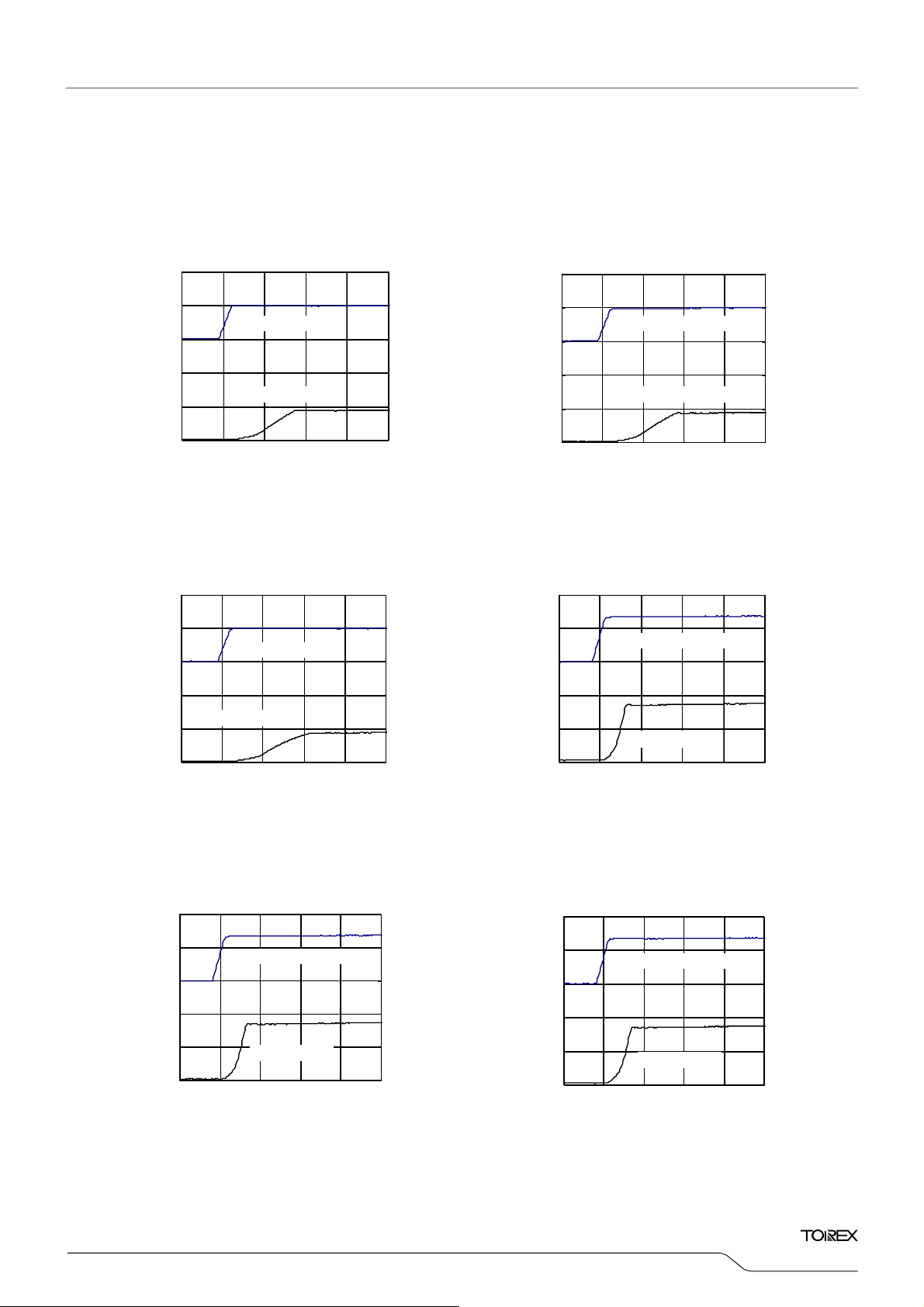
X
■
(
)
(
)
(
)
(
)
(
)
(
)
TYPICAL PERFORMANCE CHARACTERISTICS (Continued)
(15)Input Voltage Rising Response Time
V
V
=0.9V
ROUT
I
=1mA, tr= 5.0μs
=0→2.0V, CL1=4.7μF
V
4
IN1
ROUT
ceramic
5
4
ROUT
I
ROUT
=0→2.0V, CL1=4.7μF
V
IN1
=0.9V
=30mA, tr= 5.0μs
ceramic
CM524
Series
5
(V)
IN1
Input Voltage: V
(V)
IN1
Input Voltage: V
-2
-4
-6
-2
-4
-6
2
0
Inpit Voltage
Output Voltage
Time (20μs/div)
V
=0.9V
ROUT
I
=100mA, tr= 5.0μs
V
4
IN1
ROUT
=0→2.0V, CL1=4.7μF
ceramic
2
0
Inpit Voltage
Output Voltage
Time (20μs/div)
4
(V)
ROUT
3
2
1
Output Voltage: V
0
(V)
IN1
Input Voltage: V
-2
-4
-6
2
Inpit Voltage
0
4
(V)
ROUT
3
2
Output Voltage
1
Output Voltage: V
0
Time (20μs/div)
V
=1.8V
ROUT
I
=1mA, tr= 5.0μs
V
=0→2.8V, CL1=1.0μF
IN1
(V)
IN1
Input Voltage: V
4
2
0
-2
-4
5
(V)
4
ROUT
3
2
1
Output Voltage: V
0
-6
ROUT
Inpit Voltage
Output Voltage
ceramic
5
(V)
4
ROUT
3
2
1
Output Voltage: V
0
Time (20μs/div)
(V)
IN1
Input Voltage: V
-2
-4
-6
V
=1.8V
ROUT
I
=30mA, tr= 5.0μs
V
IN1
4
2
0
ROUT
=0→2.8V, CL1=1.0μF
Inpit Voltage
Output Voltage
ceramic
5
4
(V)
ROUT
3
2
1
Output Voltage: V
0
(V)
IN1
Input Voltage: V
4
2
0
-2
-4
-6
Time (20μs/div)
V
=1.8V
ROUT
I
=100mA, tr= 5.0μs
V
IN1
ROUT
=0→2.8V, CL1=1.0μF
Inpit Voltage
Output Voltage
Time (20μs/div)
ceramic
5
4
(V)
ROUT
3
2
1
Output Voltage: V
0
39/52

■
(
(
)
(
)
(
)
(
)
(
XCM524 Series
TYPICAL PERFORMANCE CHARACTERISTICS (Continued)
(15)Input Voltage Rising Response Time (Continued)
(V)
IN1
XC6405 Series (VR:2.5V )
V
=2.5V
ROUT
IOUT=1mA, tr=5.0μsec
I
=1mA, tr= 5.0μs
VIN=0→3.5V, CL=4.7μF (ceramic)
=0→3.5V, CL1=1.0μF
V
5
3
1
IN1
ROUT
Input Voltage
Inpit Voltage
ceramic)
(V)
IN1
5
3
1
5
)
4
V
(
(V)
ROUT
3
XC6405 Series (VR:2.5V )
V
ROUT
IOUT=30mA, tr=5.0μsec
I
VIN=0→3.5V, CL=4.7μF (ceramic)
V
IN1
ROUT
=0→3.5V, CL1=1.0μF
Inp u t V oltag e
Inpit Voltage
=2.5V
=30mA, tr= 5.0μs
ceramic
5
)
4
V
(V)
(
ROUT
3
-1
Input Voltage VIN (V)
-3
Input Voltage: V
-5
(V)
IN1
Input Voltage VIN (V)
Input Voltage: V
Input Voltage VIN (V)
Input Voltage: V
(V)
IN1
Input Voltage VIN (V)
Input Voltage: V
-1
Output Voltage
-3
-5
XC6405 Series (VR:3.0V )XC6405 Ser ies (V R:2.5V)
VIN=0→4.0V, CL=1.0μF (c er amic)
5
3
1
-1
-3
-5
V
Output Voltage
Time ( 20μsec/div)
Time (20μs/div)
V
=3.0V
ROUT
I
IOUT=1mA, tr=5.0μsec
=0→4.0V, CL1=1.0μF
IN1
Time ( 20μsec/div)
Time (20μs/div)
ROUT
Inp u t V oltag e
Inpit Voltage
Output Voltage
Output Voltage
=1mA, tr= 5.0μs
ceramic
2
Output Voltage
Output Voltage
Time ( 2 0μsec/div)
Time (20μs/div)
V
=2.5V
ROUT
IOUT=100mA, tr=5.0μsec
I
=100mA, tr= 5.0μs
VIN=0→3.5V, CL=4.7μF (cer a mic)
V
5
3
1
-1
-3
-5
IN1
Time ( 20μsec/div)
ROUT
=0→3.5V, CL1=1.0μF
Input Voltage
Inpit Voltage
Output Voltage
Output Voltage
Time (20μs/div)
ceramic
1
Output Voltage VOUT
Output Voltage: V
0
5
)
V
4
(
(V)
ROUT
3
2
1
Output Voltage VOUT
Output Voltage: V
0
2
1
Output Voltage VOUT
Output Voltage: V
0
5
)
4
V
(
(V)
ROUT
3
2
1
Output Voltage VOUT
Output Voltage: V
0
40/52
5
3
)
V
(V)
(
IN1
1
-1
Input Voltage VIN
-3
Input Voltage: V
-5
XC6405 Ser ie s (V R:3.0V) XC6405 Ser ies (V R:3.0V)
V
=3.0V
ROUT
IOUT=30mA, tr=5.0μsec
I
=30mA, tr= 5.0μs
VIN=0→4.0V, CL=1.0μF (ceramic)
V
IN1
Time ( 2 0μsec/div)
ROUT
=0→4.0V, CL1=1.0μF
Input Voltage
Inpit Voltage
Output Voltage
Output Voltage
Time (20μs/div)
ceramic)
)
V
(V)
(
IN1
-1
Input Voltage VIN
-3
Input Voltage: V
-5
5
3
1
5
)
4
V
(
(V)
ROUT
3
2
1
Output Voltage VOUT
Output Voltage: V
0
V
=3.0V
ROUT
IOUT=100mA, tr=5.0μsec
I
=100mA, tr= 5.0μs
VIN=0→4.0V, CL=1.0μF (ceramic)
V
IN1
ROUT
=0→4.0V, CL1=1.0μF
Input Voltage
Inpit Voltage
Output Voltage
Output Voltage
Time ( 20μsec/div)
Time (20μs/div)
ceramic
5
)
4
V
(
(V)
ROUT
3
2
1
Output Voltage VOUT
Output Voltage: V
0
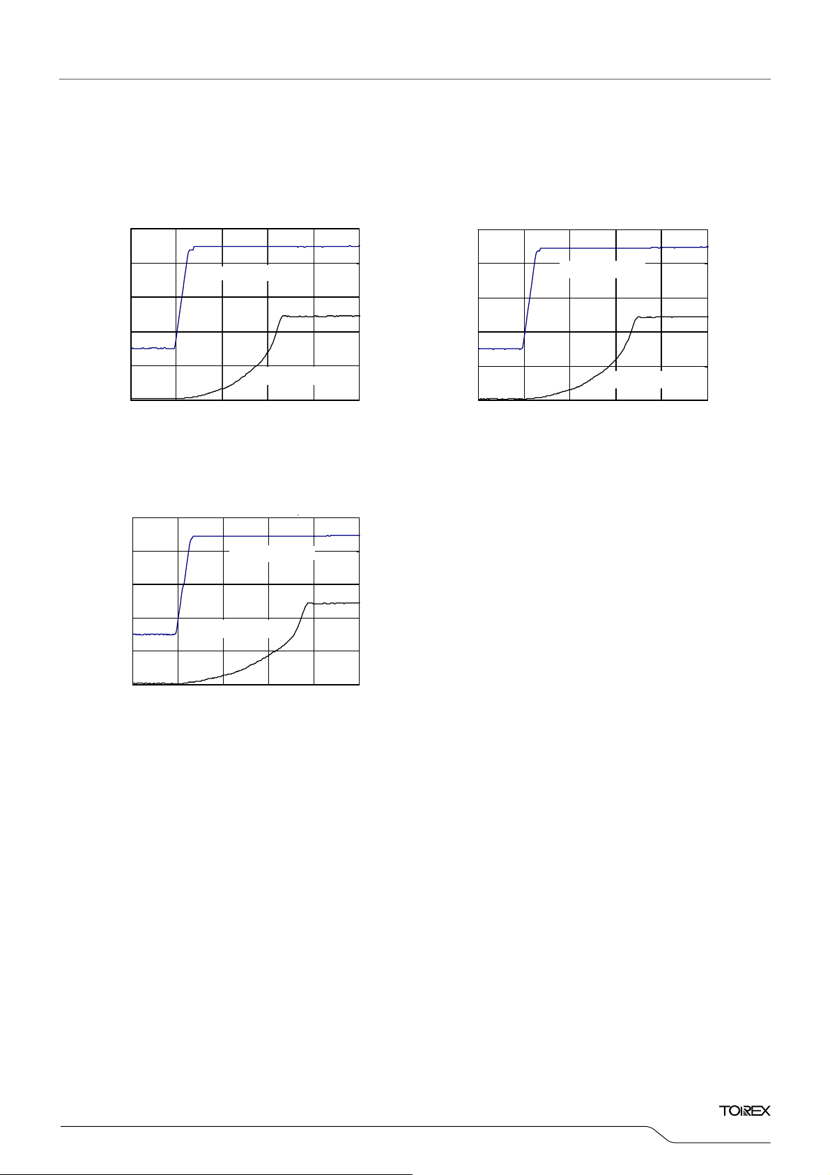
X
■
(
)
(
)
(
)
TYPICAL PERFORMANCE CHARACTERISTICS (Continued)
(15)Input Voltage Rising Response Time (Continued)
XC6405 Series (VR:5.0V )
7
V
=5.0V
ROUT
IOUT=1mA, tr=5.0μsec
I
=1mA, tr= 5.0μs
VIN=0→6.0V, CL=1.0μF (c er amic)
=0→6.0V, CL1=1.0μF
V
IN1
ROUT
ceramic
XC6405 Ser ies (VR:5.0V)
10
7
V
ROUT
VIN=0→6.0V, CL=1.0μF (c er amic)
=0→6.0V, CL1=1.0μF
V
IN1
=5.0V
IOUT=30mA, tr=5.0μsec
I
=30mA, tr= 5.0μs
ROUT
ceramic
CM524
Series
10
5
)
V
(V)
(
IN1
3
1
Input Voltage VIN
-1
Input Voltage: V
-3
7
5
)
V
(V)
(
IN1
3
1
Input Voltage VIN
-1
Input Voltage: V
-3
Input Voltage
Inpit Voltage
Output Voltage
Output Voltage
Time ( 2 0μsec/div)
Time (20μs/div)
XC6405 Ser ie s (V R:5.0V)
V
=5.0V
ROUT
IOUT=100mA, tr=5.0μsec
I
=100mA, tr= 5.0μs
VIN=0→6.0V, CL=1.0μF (c er amic)
V
IN1
Output Voltage
Output Voltage
Time ( 20μsec/div)
Time (20μs/div)
ROUT
=0→6.0V, CL1=1.0μF
Input Voltage
Inpit Voltage
ceramic
)
8
V
(V)
(
ROUT
6
4
2
Output Voltage VOUT
Output Voltage: V
0
10
)
8
V
(V)
(
ROUT
6
4
2
Output Voltage VOUT
Output Voltage: V
0
5
)
V
(V)
(
IN1
3
1
Input Voltage VIN
-1
Input Voltage: V
-3
Input Voltage
Inpit Voltage
Output Voltage
Output Voltage
Time ( 20μsec/div)
Time (20μs/div)
8
)
V
(
(V)
ROUT
6
4
2
Output Voltage VOUT
Output Voltage: V
0
41/52

)
)
XCM524 Series
■TYPICAL PERFORMANCE CHARACTERISTICS (Continued)
●2ch:DC/DC Convertor Block
(1) Efficiency vs. Output Current
V
=1.8V, f
DCOUT
V
IN2
3.6V
Output Current: I
= 4.2V
100
PWM/ PFM A ut o ma tic Sw i t c hin g Co nt r ol
90
80
70
60
50
40
30
Efficency:EFFI (%
20
10
0
0.1 1 10 100 1000
(2) Output Voltage vs. Output Current
V
=1.8V, f
2.1
DCOUT
2.0
(V)
1.9
DCOUT
PWM/ PFM A ut o ma t ic Sw i t c hing Co nt r ol
1.8
1.7
1.6
Output Voltage: V
1.5
0.1 1 10 100 1000
Output Current: I
(3) Ripple Voltage vs. Output Current
V
100
DCOUT
=1.8V, f
=1.2MHz
OSC
L=4. 7μH( NR 4018) C
PWM Control
V
3.6V
OUT 2
=1.2MHz
OSC
L=4. 7μH( NR 4018) C
V
PWM Control
OUT 2
=1.2MHz
OSC
L=4. 7μH( NR 4018) C
=4.7μF CL2=10μ F
IN2
= 4.2V
IN2
(mA)
=4.7μF CL2=10μ F
IN2
4.2V,3.6V
=
IN2
(mA)
=4.7μF CL2=10μ F
IN2
V
=1.8V, f
DCOUT
100
PWM/ PFM A ut o ma t ic Sw itc hing Co n tr o l
90
=3.0MHz
OSC
L=1. 5μH( NR 3015) C
=4.7μF CL2=10μ F
IN2
80
70
60
50
40
30
Efficency: EFFI (%
20
V
3.6V
IN2
= 4.2V
PWM Control
V
IN2
3.6V
10
0
0.1 1 10 100 1000
Output Current: I
V
=1.8V, f
DCOUT
2.1
2.0
(V)
1.9
DCOUT
PWM/ PFM A ut o ma t ic Sw itc hing Co n tr o l
OSC
L=1. 5μH( NR 3015) C
(mA)
OUT 2
=3.0MHz
IN2
V
IN2
=4.7μF CL2=10μF
=
1.8
1.7
PWM Control
1.6
Output Voltage: V
1.5
0.1 1 10 100 1000
100
Output Current: I
V
=1.8V, f
DCOUT
OSC
L=1. 5μH( NR 3015) C
(mA)
OUT 2
=3.0MHz
IN2
=4.7μF CL2=10μF
= 4.2V
4.2V,3.6V
80
60
PWM Control
40
20
Ripple Voltage: Vr (mV)
V
IN2
=
4.2V,3.6V
PWM/ PFM A ut o ma t ic
Sw itching Control
V
4.2V
=
IN2
3.6V
0
0.1 1 10 100 1000
Output Current: I
OUT 2
(mA)
80
60
PWM Control
V
4.2V,3.6V
=
IN2
40
20
Ripple Voltage: Vr (mV)
PWM/ PFM A uto ma t ic
Sw itching Control
V
4.2V
=
IN2
3.6V
0
0.1 1 10 100 1000
Output Current: I
OUT 2
(mA)
42/52

X
■TYPICAL PERFORMANCE CHARACTERISTICS (Continued)
(4) Oscillation Frequency vs. Ambient Temperature
1.5
1.4
(MHz)
OSC
1.3
1.2
1.1
1.0
0.9
Os cillation Frequency : f
0.8
V
DCOUT
=1.8V, f
=1.2MHz
OSC
L=4. 7μH( NR 4018) C
V
=3.6V
IN2
=4.7μF CL2=10μ F
IN2
-50 -25 0 25 50 75 100
Ambient Temperature: Ta (℃)
3.5
3.4
(MHz)
3.3
OSC
3.2
3.1
3.0
2.9
2.8
2.7
2.6
Oscillation F requency: f
2.5
(5) Supply Current vs. Ambient Temperature
(μA)
DD
Supply Current: I
V
DCOUT
=1.8V, f
=1.2MHz
OSC
40
35
V
=6.0V
IN2
30
V
=4.0V
25
IN2
20
15
10
5
0
-50 -25 0 25 50 75 100
Ambient Temperature: Ta (℃)
(μA)
DD
Supply Current: I
(6) Output Voltage vs. Ambient Temperature(7) UVLO Voltage vs. Ambient Temperature
V
=1.8V, f
2.1
2.0
(V)
1.9
DCOUT
DCOUT
1.8
V
OSC
IN2
=3.0MHz
=3.6V
1.8
1.5
1.2
0.9
V
DCOUT
=1.8V, f
=3.0MHz
OSC
L=1. 5μH( NR 3015) C
V
=3.6V
IN2
=4.7μF CL2=10μF
IN2
-50 -25 0 25 50 75 100
Ambient Temperature: Ta (℃)
V
DCOUT
=1.8V, f
=3.0MHz
OSC
40
V
=6.0V
35
V
=4.0V
IN2
IN2
30
25
20
15
10
5
0
-50 -25 0 25 50 75 100
Ambient Temperature: Ta (℃)
V
DCOUT
=1.8V, f
=3.0MHz
OSC
EN2 =V
IN2
CM524
Series
1.7
1.6
Output Voltage: V
1.5
-50 -25 0 25 50 75 100
Ambient Temperature: Ta (℃)
0.6
0.3
UVLO Voltage: UVLO (V)
0.0
-50 -25 0 25 50 75 100
Ambient Temperature: Ta (℃)
43/52

XCM524 Series
■TYPICAL PERFORMANCE CHARACTERISTICS (Continued)
(8) EN "H" Voltage vs. Ambient Temperature (9) EN" L" Voltage vs. Ambient Temperature
1.0
0.9
(V)
0.8
ENH
0.7
0.6
0.5
0.4
0.3
EN "H" Voltage: V
0.2
0.1
0.0
(10) Soft Start Time vs. Ambient Temperature
(ms)
SS
Soft Star t T ime: t
(11) "P-channel/N-channel" Driver on Resistance vs. Input Voltage
1.0
(Ω)
LxL
0.9
,R
0.8
LxH
0.7
0.6
0.5
0.4
0.3
0.2
0.1
Lx SW ON Resistance: R
0.0
V
DCOUT
=1.8V, f
V
OSC
IN2
=3.0MHz
=5.0V
V
IN2
=3.6V
-50 -25 0 25 50 75 100
Ambient Temperature: Ta (℃)
V
=1.8V, f
DCOUT
5
=1.2MHz
OSC
L=4. 7μH( NR 4018) C
=4.7μF CL2=10μF
IN2
4
3
2
V
=3.6V
IN2
1
0
-50 -25 0 25 50 75 100
Ambient Temperature: Ta (℃)
V
DCOUT
=1.8V, f
=3.0MHz
OSC
Nch on Resistance
Pc h on Resistanc e
0123456
Input Voltage: V
IN2
(V)
V
DCOUT
=1.8V, f
=3.0MHz
OSC
1.0
0.9
0.8
(V)
0.7
ENL
V
=5.0V
IN2
0.6
0.5
0.4
0.3
0.2
EN "L" Voltage: V
V
=3.6V
IN2
0.1
0.0
-50 -25 0 25 50 75 100
Ambient Temperature: Ta (℃)
V
=1.8V, f
DCOUT
5
=3.0MHz
OSC
L=1. 5μH( NR 3015) C
4
(ms)
SS
3
2
V
=3.6V
IN2
1
Soft Start Time: t
0
-50 -25 0 25 50 75 100
Ambient Temperature: Ta (℃)
=4.7μF CL2=10μF
IN2
44/52

X
V
f
V
f
■TYPICAL PERFORMANCE CHARACTERISTICS (Continued)
(12) XCM524xC/ XCM524xD Series Rise Wave Form
V
=5.0V
IN2
I
=1.0mA
OUT2
V
DCOUT
(13) XCM524xC/ XCM524xD Series Soft-Start Time vs. Ambient Temperature
500
V
DCOUT
400
(μs)
SS
300
200
100
Soft Star t T ime: t
0
V
I
OUT 2
-50 -25 0 25 50 75 100
(14) XCM524xC/ XCM524xD Series CL Discharge Resistance vs. Ambient Temperature
V
600
500
400
300
200
CL Discharge Resistance: Rdischg(Ω )
100
DCOUT
-50 -25 0 25 50 75 100
DCOUT
=1.2V,
L=4.7μH(NR4018) C
=1.2MHz
OSC
=4.7μF C
:0.5V/div
EN2:0.0V⇒1.0V
100μs/div
=1.2V, f
=5.0V
IN2
=1.0mA
Ambient Temperature: Ta (℃)
=3.3V, f
Ambient Temperature: Ta (℃)
=1.2MHz
OSC
L=4. 7μH( NR 4018) C
=3.0MHz
OSC
=4.7μF CL2=10μ F
IN2
VIN2=6.0V
VIN2=4.0V
=10μF
DCOUT
V
=5.0V
IN2
I
=1.0mA
OUT2
V
:1.0V/div
DCOUT
=3.3V,
L=1.5μH(NR3015) C
=3.0MHz
OSC
=4.7μF C
EN2:0.0V⇒1.0V
100μs/div
V
500
DCOUT
=3.3V, f
=3.0MHz
OSC
L=1. 5μH( NR 3015) C
IN2
400
(μs)
SS
300
200
V
=5.0V
100
Soft Star t T ime: t
I
OUT 2
IN2
=1.0mA
0
-50 -25 0 25 50 75 100
Ambient Temperature: Ta (℃)
=4.7μF CL2=10μ F
CM524
Series
=10μF
45/52

XCM524 Series
■TYPICAL PERFORMANCE CHARACTERISTICS (Continued)
(15) Load Transient Response
V
=1.2V, f
DCOUT
L=4.7μH(NR4018), C
=3.6V, EN2=V
V
IN2
I
=1mA → 100mA
OUT2
=1.2MHz(PWM/PFM Automatic Switching Control)
OSC
=4.7μF(ceramic), CL2=10μF(ceramic), Ta=25℃
IN2
IN2
1ch : I
OUT2
I
=1mA → 300mA
OUT2
1ch : I
OUT2
V
(50mV/div)
DCOUT
I
=100mA → 1mA
OUT2
V
(50mV/div)
DCOUT
1ch : I
2ch:
OUT2
2ch:
50μs/div
200μs/div
V
DCOUT
I
=300mA → 1mA
OUT2
V
DCOUT
2ch:
(50mV/div)
1ch : I
OUT2
2ch:
(50mV/div)
50μs/div
200μs/div
46/52

X
■TYPICAL PERFORMANCE CHARACTERISTICS (Continued)
(15) Load Transient Response (Continued)
V
=1.2V, f
DCOUT
L=4.7μH(NR4018), C
=3.6V, EN2=V
V
IN2
I
=1mA → 100mA
OUT2
V
(50mV/div)
DCOUT
=1.2MHz (PWM Control)
OSC
=4.7μF(ceramic), CL2=10μF(ceramic), Ta=25℃
IN2
IN2
1ch : I
OUT2
2ch:
I
=1mA → 300mA
OUT2
V
(50mV/div)
DCOUT
1ch : I
OUT2
2ch:
CM524
Series
I
=100mA → 1mA
OUT2
V
DCOUT
1ch : I
OUT2
2ch:
(50mV/div)
50μs/div
200μs/div
I
=300mA → 1mA
OUT2
V
(50mV/div)
DCOUT
1ch : I
50μs/div
OUT2
2ch:
200μs/div
47/52
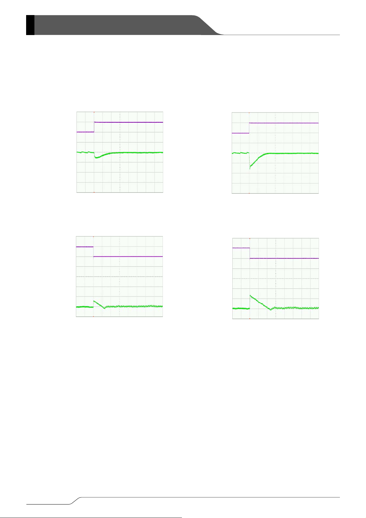
XCM524 Series
■TYPICAL PERFORMANCE CHARACTERISTICS (Continued)
(15) Load Transient Response (Continued)
V
=1.8V, f
DCOUT
L=1.5μH(NR3015), C
=3.6V, EN=V
V
IN2
I
=1mA → 100mA
OUT2
V
(50mV/div)
DCOUT
I
=100mA → 1mA
OUT2
V
(50mV/div)
DCOUT
=3.0MHz (PWM/PFM Automatic Switching Control)
OSC
=4.7μF(ceramic), CL2=10μF(ceramic),Ta=25℃
IN2
IN2
1ch : I
OUT2
2ch:
50μs/div
1ch : I
OUT2
2ch:
200μs/div
I
=1mA → 300mA
OUT2
V
(50mV/div)
DCOUT
I
=300mA → 1mA
OUT2
V
(50mV/div)
DCOUT
1ch : I
1ch : I
OUT2
2ch:
50μs/div
OUT2
2ch:
200μs/div
48/52

X
■TYPICAL PERFORMANCE CHARACTERISTICS (Continued)
(15) Load Transient Response (Continued)
V
=1.8V, f
DCOUT
L=1.5μH(NR3015), C
=3.6V, EN2=V
V
IN2
I
=1mA → 100mA
OUT2
V
(50mV/div)
DCOUT
I
=100mA → 1mA
OUT2
V
DCOUT
(50mV/div)
=3.0MHz (PWM Control)
OSC
=4.7μF(ceramic), CL2=10μF(ceramic), Ta=25℃
IN2
IN2
1ch : I
OUT2
2ch:
1ch : I
OUT2
2ch:
50μs/div
200μs/div
I
=1mA → 300mA
OUT2
V
DCOUT
I
=300mA → 1mA
OUT2
V
(50mV/div)
DCOUT
1ch : I
OUT2
2ch:
(50mV/div)
1ch : I
OUT2
2ch:
50μs/div
200μs/div
CM524
Series
49/52
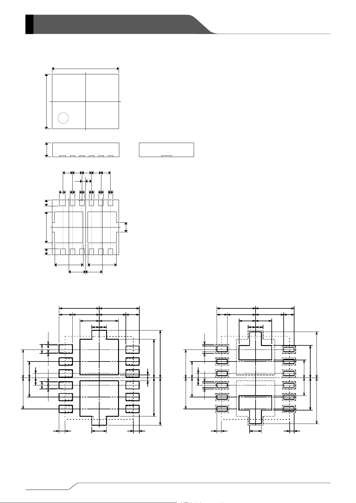
■
XCM524 Series
PACKAGING INFORMATION
●USP-12B01
2.3±0.08
MAX0.6
0.25±0.11.3±0.10.25±0.1
0.25±
0.05
●USP-12B01 Reference Pattern Layout●USP-12B01 Reference Metal Mask Design
0.95
0.55
0.65
1.05
0 .0250.025
0.30
0.25 0.15
0.25
0 . 025 0.025
0.20 0.200.50
2.8±0.08
(0.4) (0.4) (0.4) (0.4) (0.4)
(0.15) (0.25)
0.2±
0.05
0.2±
0.05
0.2±
0.05
0.2±
0.05
0.2±
0.05
123456
0.4±0.1
1.2±0.1
0.7±0.050.7±0.05
1.35
0.45 0.45
0.90
0.65 0.65
0.250.25
1.2±0.1
78912 11 10
1.35
0.90
1.30
0.35 0.35
0.95
0.55
1.30
0.95
0.55
0.250.25
0.05
0.200.05
1.60
1.30
0.95
0.55
0.10 0.10
1.30
1.60
0.25 0.15
0.150.05 0.05
0.65
1.05
0.150.15 0.40
1.55
1.10
0.60
0.60
1.10
1.55
50/52

X
■PACKAGING INFORMATION (Continued)
● USP-12B01 Power Dissipation
Power dissipation data for the USP-12B01 is shown in this page.
The value of power dissipation varies with the mount board conditions.
Please use this data as one of reference data taken in the described condition.
1. Measurement Condition (Reference data)
Condition: Mount on a board
Ambient: Natural convection
Soldering: Lead (Pb) free
Board: Dimensions 40 x 40 mm (1600 mm
st
Layer: Land and a wiring pattern
1
nd
Layer: Connecting to approximate 50% of the 1
2
rd
Layer: Connecting to approximate 50% of the 2
3
th
Layer: Noting
4
Material: Glass Epoxy (FR-4)
Thickness: 1.6 mm
Through-hole: 2 x 0.8 Diameter (each TAB needs one through-hole)
2. Power Dissipation vs. Ambient Temperature
●Only 1ch heating, Board Mount (Tj max = 125℃)
Ambient Temperature(℃) Power Dissipation Pd(mW) Thermal Resistance (℃/W)
25 800
85 320
1000
●Both 2ch heating same time, Board Mount (Tj max = 125℃)
800
600
400
200
許容損失Pd(mW)
0
25 45 65 85 105 125
Power Dissipation: Pd (mW)
Pd-Ta特性
Pd vs. Ta
Ambient Temperature: Ta (℃)
周囲温度
Ambient Temperature(℃) Power Dissipation Pd(mW) Thermal Resistance (℃/W)
25 600
85 240
許容損失Pd(mW)
Power Dissipation: Pd (mW)
1000
800
600
400
200
0
25 45 65 85 105 125
Pd-Ta特性グラフ
Pd vs. Ta
Ambient Temperature: Ta (℃)
周囲温度Ta(℃)
グラフ
Ta(℃)
2
in one side)
st
heat sink
nd
heat sink
Evaluation Board (Unit: mm)
125.00
166.67
CM524
Series
51/52

XCM524 Series
1. The products and product specifications contained herein are subject to change without
notice to improve performance characteristics. Consult us, or our representatives
before use, to confirm that the information in this datasheet is up to date.
2. We assume no responsibility for any infringement of patents, patent rights, or other
rights arising from the use of any information and circuitry in this datasheet.
3. Please ensure suitable shipping controls (including fail-safe designs and aging
protection) are in force for equipment employing products listed in this datasheet.
4. The products in this datasheet are not developed, designed, or approved for use with
such equipment whose failure of malfunction can be reasonably expected to directly
endanger the life of, or cause significant injury to, the user.
(e.g. Atomic energy; aerospace; transport; combustion and associated safety
equipment thereof.)
5. Please use the products listed in this datasheet within the specified ranges.
Should you wish to use the products under conditions exceeding the specifications,
please consult us or our representatives.
6. We assume no responsibility for damage or loss due to abnormal use.
7. All rights reserved. No part of this datasheet may be copied or reproduced without the
prior permission of TOREX SEMICONDUCTOR LTD.
52/52
 Loading...