

TOREX XCM517 User Manual
XCM517 Series
600mA Synchronous Dual Output Step-Down DC/DC Converter
■GENERAL DESCRIPTION
The XCM517 series is a multi combination module IC which comprises of two 600mA driver transistor built-in synchronous
step–down DC/DC converter. The XCM517 series is available in an ultra small package USP-12B01 suited for space
conscious applications.
The XCM517 series is a group of synchronous-rectification type DC/DC converters with a built-in 0.42ΩP-channel MOS driver
transistor and 0.52ΩN-channel MOS switching transistor, designed to allow the use of ceramic capacitors. The ICs enable a
high efficiency, stable power supply with an output current of 600mA to be configured using only a coil and two capacitors
connected externally. Operating voltage range is from 2.7V to 6.0V. With the built-in oscillator, either 1.2MHz or 3.0MHz can
be selected for suiting to your particular application. As for operation mode, the XCM517xA / XCM517xB series are PWM
control, the XCM517xC / XCM517xD series are automatic PWM/PFM switching control, allowing fast response, low ripple and
high efficiency over the full range of loads (from light load to heavy load).
The soft start and current control functions are internally optimized. During stand-by, all circuits are shutdown to reduce
current consumption to as low as 1.0μA or less. With the built-in UVLO (Under Voltage Lock Out) function, the internal
P-channel driver transistor is forced OFF when input voltage becomes 1.4V or lower.
■APPLICATIONS
●Mobile phones, Smart phones
●Bluetooth equipment
●Personal Device Assistances
●Portable games
●Digital still cameras, camcorders
■
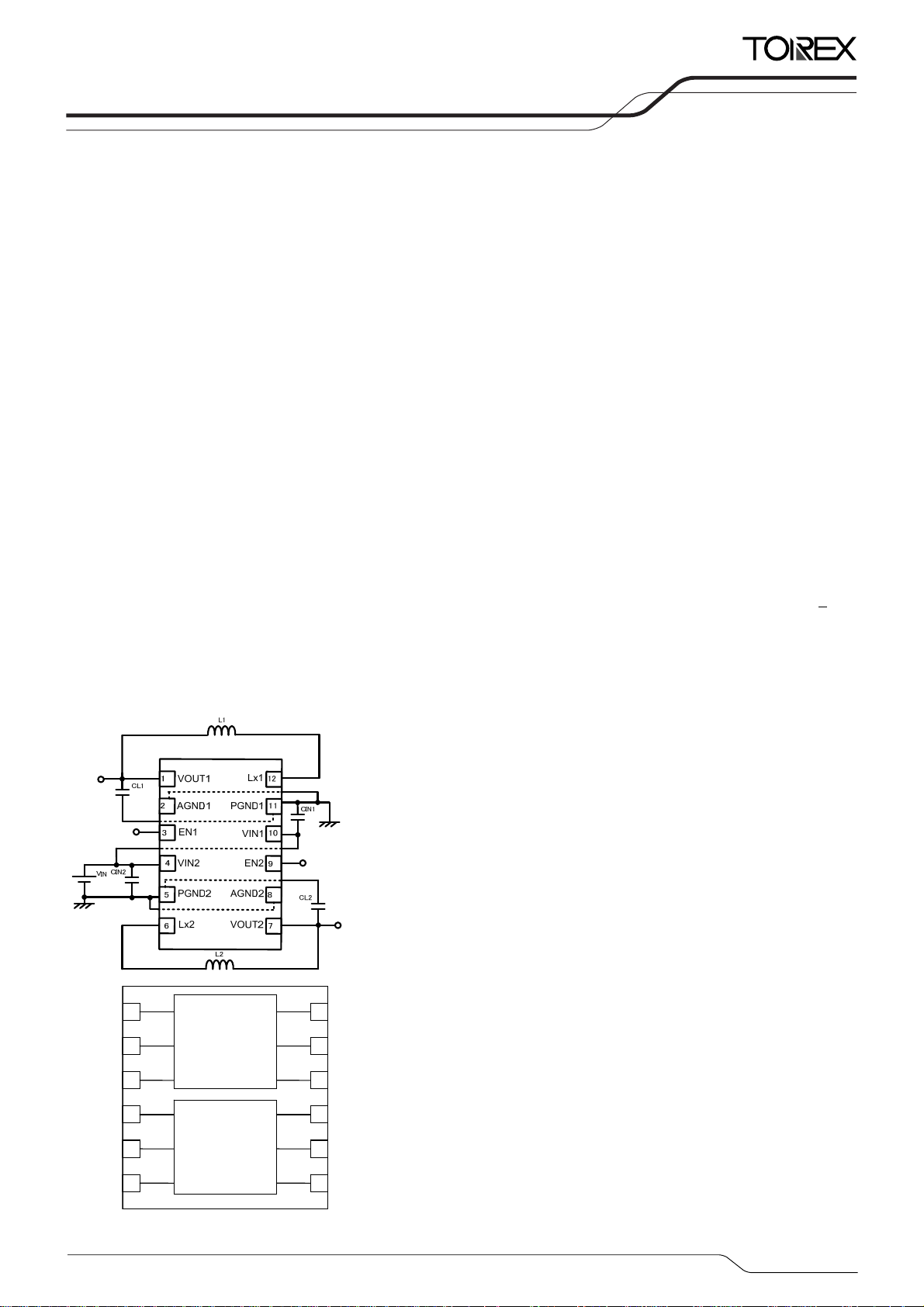
TYPICAL APPLICATION CIRCUIT
AGND1
1
VOUT
2
XC9235/XC9236
AGND
Lx
PGND
VOUT1
12
11
Lx1
PGND1
■FEATURES
P-channel MOS Driver Transistor Built-In
N-channel MOS Switching Transistor Built-In
Input Voltage Range
High Efficiency : 92% (TYP.)
Output Current : 600mA
Oscillation Frequency : 1.2MHz, 3.0MHz (+15%)
Maximum Duty Cycle
Soft-Start Circuit Built-In
Current Limiter Circuit Built-In (Constant Current & Latching)
Ceramic Capacitor Compatible
Control Methods : PWM (XCM517xA / XCM517xB)
*Performance depends on external components and wiring on the PCB.
Combination of voltage 1 ch 2ch
XCM517xx01D 1.2V 1.8V
XCM517xx02D 1.2V 3.3V
XCM517xx03D 1.8V 3.3V
XCM517xx06D 1.5V 1.8V
XCM517xx07D 1.5V 3.3V
*The other combination of voltage is semi-custom.
Environmentally Friendly : EU RoHS Compliant, Pb Free
* The dotted lines in the circuit indicates the connection using through-holes at the
backside of the PC board
: ON resistance 0.42Ω
: ON resistance 0.52Ω
: 2.7V ~ 6.0V
: 100%
PWM/PFM Auto (XCM517xC / XCM517xD)
ETR2425-008
EN1
3
CE
VIN2
4
VIN
PGND2
Lx2
5
6
XC9235/XC9236
Lx
(TOP VIEW)
VOUT
VIN
CE
10
9
8
7
VIN1
EN2
AGND2
VOUT2
1/28
XCM517 Series
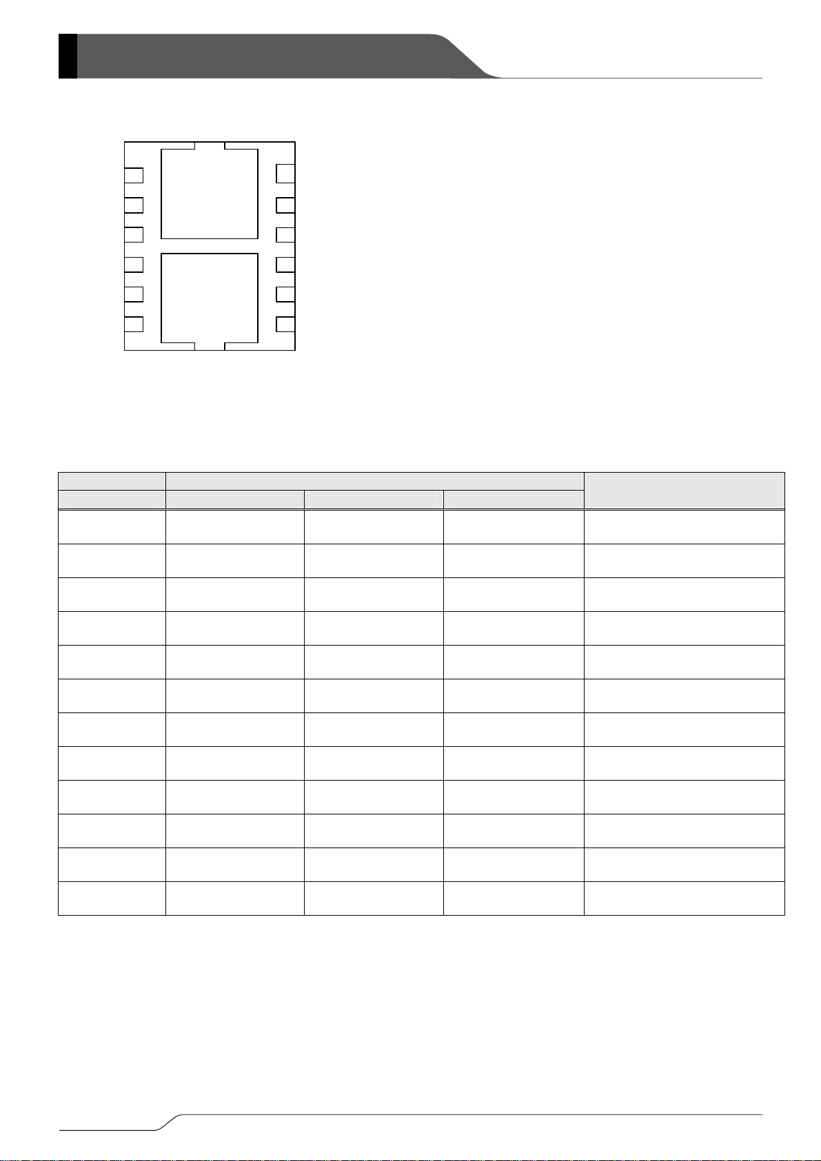
■PIN CONFIGURATIOIN
LX112
PGND1 11
VIN1 10
EN2 9
AGND2 8
VOUT2 7
■PIN ASSIGNMENT
*1
*2
USP-12B01
(BOTTOM VIEW)
1 VOUT1
2 AGND1
3 EN1
4 VIN2
5 PGND2
6 Lx2
PIN NUMBER PIN NAME
USP-12B01 XCM517 XC9235/XC9236 XC9235/XC9236
1 V
V
OUT1
―
OUT
2 AGND1 AGND ―
3 EN1 CE ―
4 V
― V
IN2
IN
5 PGND2 ― PGND
6 Lx2 ― Lx
7 V
― V
OUT2
OUT
8 AGND2 ― AGND
9 EN2 ― CE
10 V
V
IN1
―
IN
11 PGND1 PGND ―
12 Lx1 Lx ―
NOTE:
* A dissipation pad on the reverse side of the package should be electrically isolated.
*1: Electrical potential of the DC/DC 1 channels’ dissipation pad should be V
*2: Electrical potential of the DC/DC 2 channels’ dissipation pad should be V
Care must be taken for an electrical potential of each dissipation pad so as to enhance mounting strength and heat release when the pad
needs to be connected to the circuit.
level.
SS
level.
SS
DC/DC-1 Channel Block:
Output Voltage sense
DC/DC-1 Channel Block:
Analog Ground
DC/DC-1 Channel Block:
ON/OFF Control
DC/DC-2 Channel Block:
Power Input
DC/DC-2 Channel Block :
Power Ground
DC/DC-2 Channel Block :
Switching
DC/DC-2 Channel Block :
Output Voltage sense
DC/DC-2 Channel Block :
Analog Ground
DC/DC-2 Channel Block :
ON/OFF Control
DC/DC-1 Channel Block :
Power Input
DC/DC-1 Channel Block :
Power Ground
DC/DC-1 Channel Block :
Switching
FUNCTIONS
2/28
r
XCM517
Series
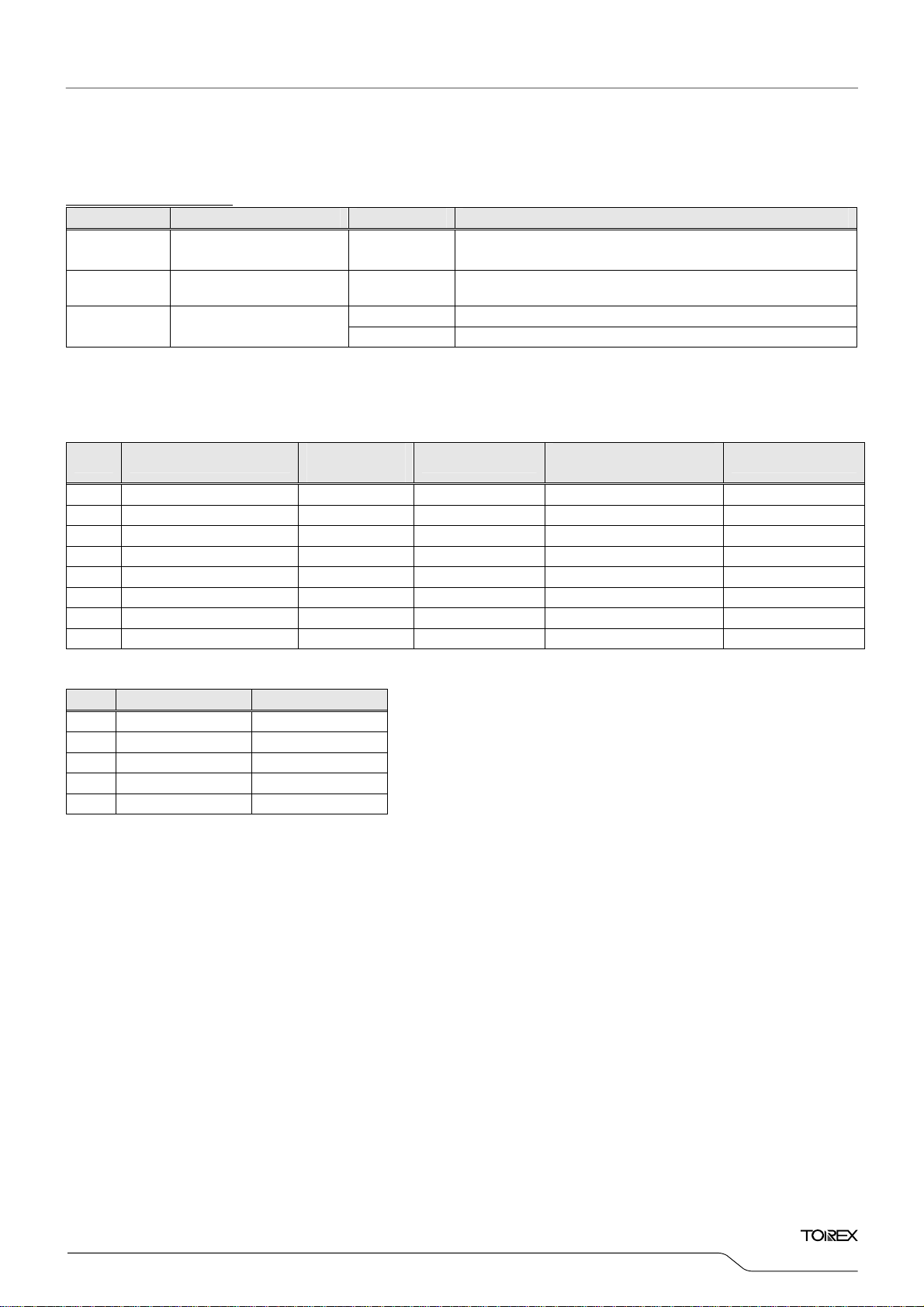
■PRODUCT CLASSIFICATION
●Ordering Information
XCM517①②③④⑤⑥-⑦
DESIGNATOR DESCRIPTION SYMBOL DESCRIPTION
①②
Frequency and Options
③④ Output Voltage -
⑤⑥-⑦
(*1)
The “-G” suffix indicates that the products are Halogen and Antimony free as well as being fully RoHS compliant.
(*2)
The device orientation is fixed in its embossed tape pocket. For reverse orientation, please contact your local Torex sales office o
representative. (Standard orientation: ⑤R-⑦, Reverse orientation: ⑤L-⑦)
(*1)
Control, Oscillation
Packages
Taping Type
(*2)
- See the chart below
Internally set sequential number relating to output voltage
(See the chart below)
DR USP-12B01
DR-G USP-12B01
DESIGNATOR ①②
①② CONTROL
OCSILLATION
FREQUENCY
CL DISCHARGE
HIGH SPEED
SOFT-START
EN INPUT LOGIC
AA PWM Control 1.2M Not Available Not Available High Active
AB PWM Control 3.0M Not Available Not Available High Active
AC PWM/PFM Auto 1.2M Not Available Not Available High Active
AD PWM/PFM Auto 3.0M Not Available Not Available High Active
BA PWM Control 1.2M Available Available High Active
BB PWM Control 3.0M Available Available High Active
BC PWM/PFM Auto 1.2M Available Available High Active
BD PWM/PFM Auto 3.0M Available Available High Active
DESIGNATOR ③④ Output Voltage
③④ V
V
OUT1
OUT2
01 1.2 1.8
02 1.2 3.3
03 1.8 3.3
06 1.5 1.8
07 1.5 3.3
*This series are semi-custom products. For other combinations, output voltages and etc., please ask Torex sales contacts.
3/28
XCM517 Series
■BLOCK DIAGRAMS
V
OUT
R2
R1
V
IN
Vref with
Soft Start,
CE
V
SS
R3
R4
XC9235A/XC9236A XC9235B/XC9236B
Available with CL Discharge, High Speed Soft-Start
Phase
Error Amp.
UVLO
VSHORT
Compensation
PWM/PFM
Selector
UVLO Cmp
PWM
Comparator
Current Feedback
Current Limit
Logic
Synch
Buffer
Drive
Ramp Wave
Generator
OSC
CE/MODE
Control
Logic
Lx
CE
V
OUT
V
IN
V
SS
NOTE: The signal from CE/MODE Control Logic to PWM/PFM Selector is being fixed to "L" level inside,
and XC9235 series chooses only PWM control.
The signal from CE/MODE Control Logic to PWM/PFM Selector is being fixed to "H" level inside,
and XC9236 series chooses only PWM/PFM automatic switching control.
Diodes inside the circuit are ESD protection diodes and parasitic diodes.
*Diodes inside the circuit are an ESD protection diode and a parasitic diode.
■MAXIMUM ABSOLUTE RATINGS
PAR AMETE R SYMBOL RATINGS UNITS
V
/ V
IN1
Voltage V
IN2
Lx1 / Lx2 Voltage VLx1 / VL
V
/ V
OUT1
Voltage V
OUT2
EN1 / EN2 Voltage V
IN1
OUT1
EN1
/ V
- 0.3 ~ 6.5 V
IN2
- 0.3 ~ V
x2
/ V
- 0.3 ~ 6.5 V
OUT2
/ V
- 0.3 ~ 6.5 V
EN2
Lx1 / Lx2 Current ILx1 / ILx2 ±1500 mA
Power Dissipation (Ta=25℃) USP-12B01 Pd 150 mW
Junction Temperature Tj 125 ℃
Operating Temperature Range Topr - 40 ~ + 85 ℃
Storage Temperature Range Tstg - 55 ~ + 125 ℃
XC9235B / XC9236B Series XC9235A / XC9236A Series
、)(CL放電機能有 高速ソフトスタート
Phase
Compensation
R2
Error Amp.
R1
VSHORT
Vref with
PWM/PFM
Soft Start,
Selector
CE
UVLO Cmp
UVLO
R3
R4
+ 0.3 or 6.5 V
IN1
PWM
Comparator
Current Feedback
Current Limit
Logic
Synch
Buffer
Drive
Ramp Wave
Generator
OSC
CE/MODE
Control
Logic
CE/
Lx
CE
4/28
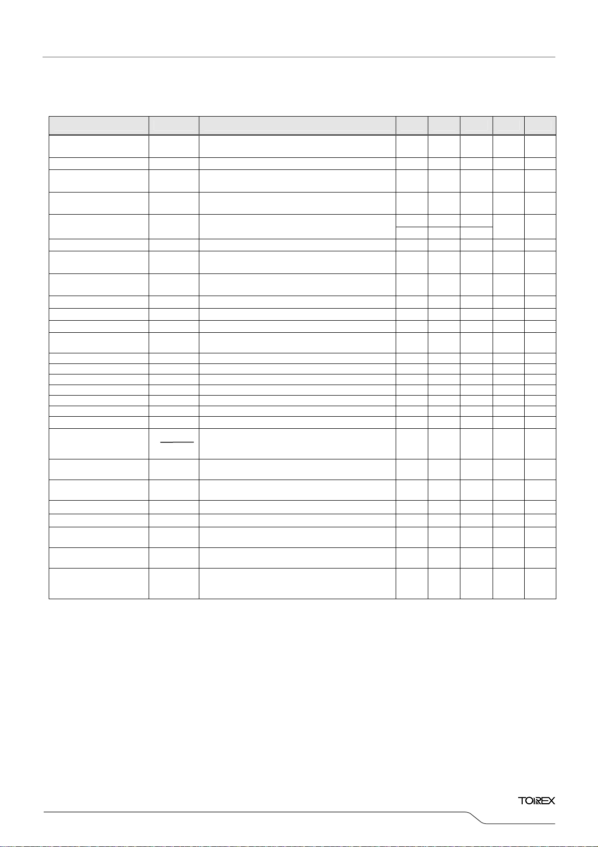
■ELECTRICAL CHARACTERISTICS
●XCM517Ax, 1ch Block /2ch Block V
OUT
=1.8V, f
=1.2MHz, Ta=25℃
OSC
XCM517
Series
PARAMETER SYMBOL CONDITIONS MIN. TYP. MAX. UNITS
Output Voltage V
OUT
When connected to external components,
V
IN=VEN
=5.0V, I
OUT1
=30mA
1.764 1.800 1.836 V ①
Operating Voltage Range VIN 2.7 - 6.0 V ①
Maximum Output Current I
UVLO Voltage V
OUTMAX
UVLO
Supply Current IDD V
Stand-by Current I
Oscillation Frequency f
PFM Switching Current I
Maximum I
Limit MAX I
PFM
STB
OSC
PFM
Maximum Duty Ratio MAXDTY VIN=VEN5.0V, V
Minimum Duty Ratio MINDTY VIN=VEN5.0V, V
Efficiency
Lx SW "H" ON Resistance 1 R
Lx SW "H" ON Resistance 2 R
Lx SW "L" ON Resistance 1 R
Lx SW "L" ON Resistance 2 R
Lx SW "H" Leak Current
Lx SW "L" Leak Current
Current Limit
Output Voltage
Temperature
Characteristics
EN "H" Level Voltage V
EN "L" Level Voltage V
EN "H" Current I
EN "L" Current I
(*2)
EFFI
LxH
LxH
LxL
(*5)
(*5)
(*9)
ILIM VIN=VEN=5.0V, V
LxL
ILeakH VIN=V
ILeakL VIN=V
△
V
OUT
V
・△
OUT
ENH
ENL
ENH
ENL
Soft Start Time tSS
Latch Time t
Short Protection
Threshold Voltage
V
LAT
SHORT
Test conditions: Unless otherwise stated, VIN = 5.0V, V
When connected to external components,
V
IN=VOUT(E)
V
EN=VIN,VOUT
Voltage which Lx pin holding “L” level
IN=VEN
V
PFM
IN
When connected to external components,
V
IN=VOUT(E)
When connected to external components,
V
IN=VOUT(E)
VEN=VIN=(C-1) I
+2.0V, VEN=1.0V
=0V,
=5.0V, V
OUT=VOUT(E)
=5.0V, VEN=0V, V
+2.0V,VEN=1.0V, I
+2.0V, VEN=VIN , I
OUT
OUT=VOUT (E)
OUT=VOUT (E)
=1mA
When connected to external components,
V
EN=VIN=VOUT (E)
VIN=VEN=5.0V, V
VIN=VEN=3.6V, V
VIN=VEN=5.0V
VIN=VEN=3.6V,
OUT
OUT
I
=30mA
OUT
topr
-40℃≦Topr≦85℃
V
=0V, Applied voltage to V
OUT
Voltage changes Lx to “H” level
V
=0V, Applied voltage to V
OUT
Voltage changes Lx to “L” level
VIN=VEN=5.0V, V
V
=5.0V, VEN=0V, V
IN
+1.2V
OUT
OUT
(*4)
- 0.45 0.66 Ω -
(*4)
- 0.52 0.77 Ω -
=5.0V, VEN=0V, LX=0V - 0.01 1.0 μA ⑤
=5.0V, VEN=0V, LX=5.0V - 0.01 1.0 μA ⑤
OUT=VOUT (E)
OUT
(*8)
×1.1V
OUT=VOUT(E)
OUT
(*11)
200 % ①
×0.9V 100 - - % ②
×1.1V - - 0 % ②
(*7)
, I
OUT
=0V,ILX =100mA
=0V,ILX =100mA
×0.9V
=0V - 0.1 0. μA ⑤
=0V - 0.1 - 0.1 μA ⑤
OUT
When connected to external components,
V
=0V → VIN , I
EN
V
= VEN=5.0V, V
IN
Short Lx at 1Ω resistance
Sweeping V
1Ω resistance, V
=1mA
OUT
=0.8× V
OUT
, VIN=VEN= 5.0V, Short Lx at
OUT
OUT
(*6)
voltage which Lx becomes “L”
level within 1ms
= Setting voltage
OUT (E)
(*1, *10)
(XCM517AA) - 22 50
(XCM517AC) - 15 33
600 - - mA ①
1.00 1.40 1.78 V ③
μA ②
×1.1V - 0 1.0 μA ②
=100mA
OUT
=1mA
=100mA
(*11)
(*3)
- 0.35 0.55 Ω ④
(*3)
- 0.42 0.67 Ω ④
(*7)
900 1050 1350 mA ⑥
1020 1200 1380 kHz ①
120 160 200 mA ①
- 92 - % ①
- ±100 - ppm/ ℃ ①
EN,
EN,
(*10)
(*10)
0.65 - 6.0 V ③
V
- 0.25 V ③
SS
0.5 1.0 2.5 ms ①
,
OUT(E)
1.0 - 20.0 ms ⑦
0.675 0.900 1.125 V ⑦
NOTE:
*1: Including hysteresis width of operating voltage.
*2: EFFI = { ( output voltage×output current ) / ( input voltage×input current) }×100
*3: ON resistance (Ω)= (V
- Lx pin measurement voltage) / 100mA
IN
*4: Design value
*5: When temperature is high, a current of approximately 10μA (maximum) may leak.
*6: Time until it short-circuits DC
with GND via 1Ωof resistor from an operational state and is set to Lx=0V from current limit pulse
OUT
generating.
*7: When V
+1.2V<2.7V, VIN=2.7V
OUT(E)
*8: When the difference between the input and the output is small, some cycles may be skipped completely before current maximizes.
If current is further pulled from this state, output voltage will decrease because of P-channel driver ON resistance.
*9: Current limit denotes the level of detection at peak of coil current.
*10: "H"=V
*11: XCM517xA / XCM517xB series exclude I
- 1.2V, "L"=+ 0.1V ~ - 0.1V
IN~VIN
and MAXI
PFM
because those are only for the PFM control’s functions.
PFM
*12: The electrical characteristics shows 1 channel values when the other channel is stopped.
CIRCUIT
5/28
XCM517 Series
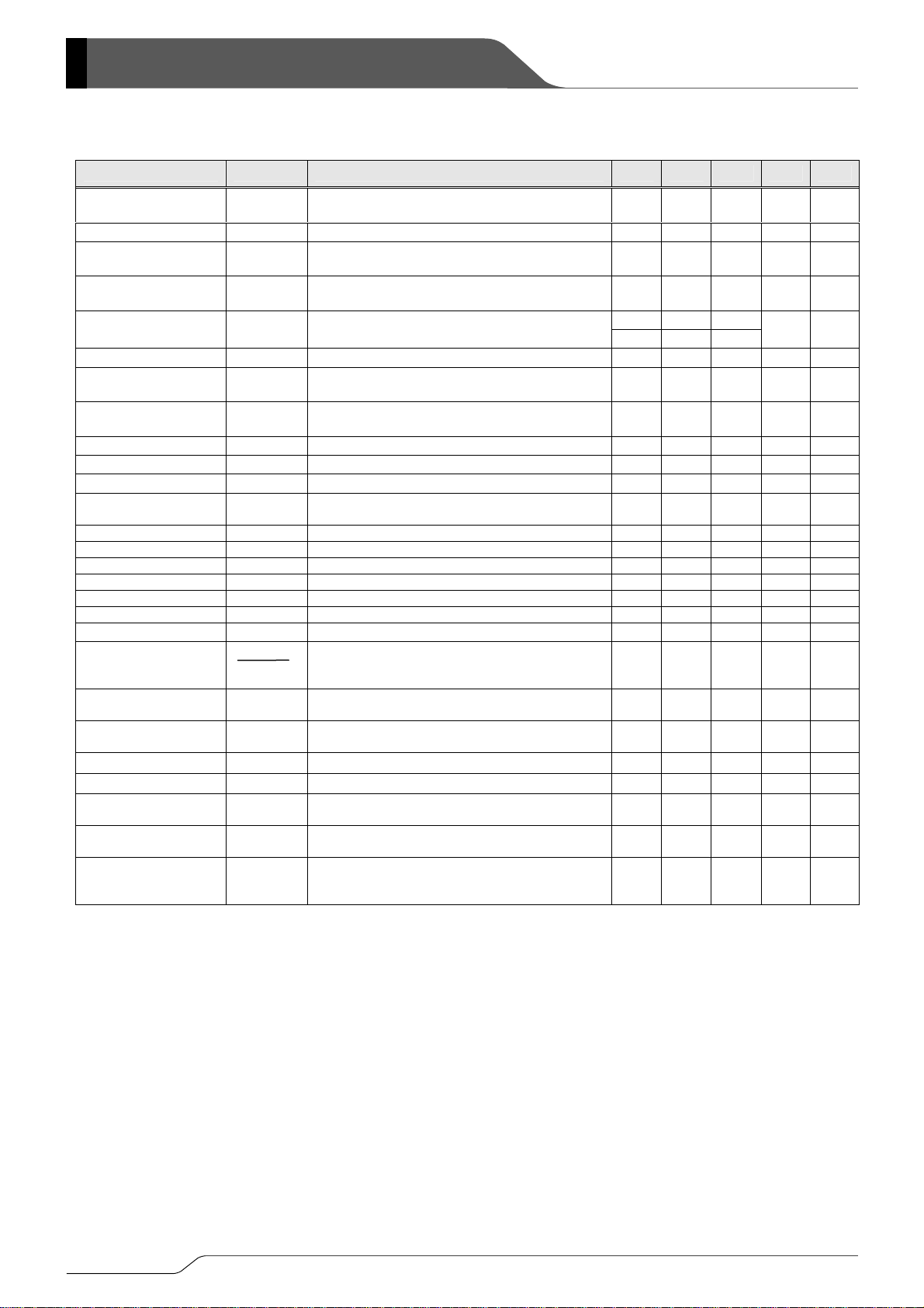
■ELECTRICAL CHARACTERISTICS (Continued)
●XCM517Ax, 1ch Block / 2ch Block V
OUT
=1.8V, f
=3.0MHz, Ta=25℃
OSC
PARAMETER SYMBOL CONDITIONS MIN. TYP. MAX. UNITS
Output Voltage V
OUT
When connected to external components,
V
IN=VEN
=5.0V, I
OUT1
=30mA
1.764 1.800 1.836 V ①
Operating Voltage Range VIN 2.7 - 6.0 V ①
Maximum Output Current I
UVLO Voltage V
OUTMAX
UVLO
Supply Current IDD V
Stand-by Current I
Oscillation Frequency f
PFM Switching Current I
Maximum I
Limit MAX I
PFM
STB
OSC
PFM
Maximum Duty Ratio MAXDTY VIN=VEN5.0V, V
Minimum Duty Ratio MINDTY VIN=VEN5.0V, V
Efficiency
Lx SW "H" ON Resistance 1 R
Lx SW "H" ON Resistance 2 R
Lx SW "L" ON Resistance 1 R
Lx SW "L" ON Resistance 2 R
Lx SW "H" Leak Current
Lx SW "L" Leak Current
Current Limit
Output Voltage
Temperature
Characteristics
EN "H" Level Voltage V
EN "L" Level Voltage V
EN "H" Current I
EN "L" Current I
(*2)
EFFI
LxH
LxH
LxL
(*5)
(*5)
(*9)
ILIM V
LxL
ILeakH VIN=V
ILeakL VIN=V
△
V
OUT
・△
V
OUT
ENH
ENL
ENH
ENL
Soft Start Time tSS
Latch Time t
Short Protection
Threshold Voltage
V
LAT
SHORT
Test conditions: Unless otherwise stated, VIN = 5.0V, V
When connected to external components,
V
IN=VOUT(E)
V
V
PFM
EN=VIN,VOUT
Voltage which Lx pin holding “L” level
IN=VEN
IN
When connected to external components,
V
IN=VOUT(E)
When connected to external components,
V
IN=VOUT(E)
VEN=VIN=(C-1) I
When connected to external components,
V
EN=VIN=VOUT (E)
VIN=VEN=5.0V, V
VIN=VEN=3.6V, V
VIN=VEN=5.0V
VIN=VEN=3.6V,
IN=VEN
I
OUT
topr
-40℃≦Topr≦85℃
V
V
V
OUT
Voltage changes Lx to “H” level
V
OUT
Voltage changes Lx to “L” level
IN=VEN
IN
+2.0V, VEN=1.0V
=0V,
=5.0V, V
OUT=VOUT(E)
=5.0V, VEN=0V, V
OUT=VOUT(E)
+2.0V,VEN=1.0V, I
+2.0V, VEN=VIN , I
(*11)
=1mA
OUT
OUT=VOUT (E)
OUT=VOUT (E)
+1.2V
OUT
OUT
(*4)
- 0.45 0.66 Ω -
(*4)
- 0.52 0.77 Ω -
=5.0V, VEN=0V, LX=0V - 0.01 1.0 μA ⑤
OUT
=5.0V, VEN=0V, LX=5.0V - 0.01 1.0 μA ⑤
OUT
=5.0V, V
OUT=VOUT (E)
×0.9V 100 - - % ②
×1.1V - - 0 % ②
(*7)
, I
=0V,ILX =100mA
=0V,ILX =100mA
=30mA
=0V, Applied voltage to V
=0V, Applied voltage to V
=5.0V, V
=5.0V, VEN=0V, V
=0V - 0.1 0. μA ⑤
OUT
=0V - 0.1 - 0.1 μA ⑤
OUT
When connected to external components,
V
=0V → VIN , I
EN
V
= VEN=5.0V, V
IN
Short Lx at 1Ω resistance
Sweeping V
1Ω resistance, V
=1mA
OUT
=0.8× V
OUT
, VIN=VEN= 5.0V, Short Lx at
OUT
voltage which Lx becomes “L”
OUT
level within 1ms
= Setting voltage
OUT (E)
(*8)
×1.1V
(*1, *10)
(XCM517AB) - 46 65
(XCM517AD) - 21 35
600 - - mA ①
1.00 1.40 1.78 V ③
μA ②
×1.1V - 0 1.0 μA ②
=100mA
OUT
=1mA
OUT
(*11)
2550 3000 3450 kHz ①
170 220 270 mA ①
200 300 % ①
=100mA
OUT
×0.9V
(*3)
- 0.35 0.55 Ω ④
(*3)
- 0.42 0.67 Ω ④
(*7)
900 1050 1350 mA ⑥
- 86 - % ①
- ±100 - ppm/ ℃ ①
EN,
EN,
(*10)
(*10)
0.65 - 6.0 V ③
V
- 0.25 V ③
SS
0.5 1.0 2.5 ms ①
,
OUT(E)
(*6)
1.0 - 20.0 ms ⑦
0.675 0.900 1.125 V ⑦
NOTE:
*1: Including hysteresis width of operating voltage.
*2: EFFI = { ( output voltage×output current ) / ( input voltage×input current) }×100
*3: ON resistance (Ω)= (V
- Lx pin measurement voltage) / 100mA
IN
*4: Design value
*5: When temperature is high, a current of approximately 10μA (maximum) may leak.
*6: Time until it short-circuits DC
with GND via 1Ωof resistor from an operational state and is set to Lx=0V from current limit pulse
OUT
generating.
*7: When V
+1.2V<2.7V, VIN=2.7V
OUT(E)
*8: When the difference between the input and the output is small, some cycles may be skipped completely before current maximizes.
If current is further pulled from this state, output voltage will decrease because of P-channel driver ON resistance.
*9: Current limit denotes the level of detection at peak of coil current.
*10: "H"=V
*11: XCM517xA / XCM517xB series exclude I
- 1.2V, "L"=+ 0.1V ~ - 0.1V
IN~VIN
and MAXI
PFM
because those are only for the PFM control’s functions.
PFM
*12: The electrical characteristics shows 1 channel values when the other channel is stopped.
CIRCUIT
6/28
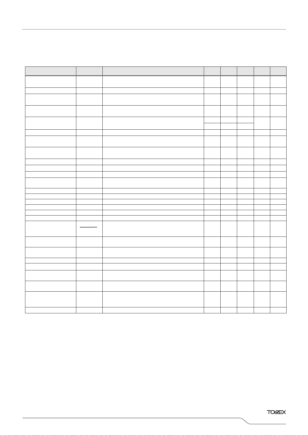
■ELECTRICAL CHARACTERISTICS (Continued)
●XCM517Bx, 1ch Block / 2ch Block V
OUT
=1.8V, f
=1.2MHz, Ta=25℃
OSC
XCM517
Series
PARAMETER SYMBOL CONDITIONS MIN. TYP. MAX. UNITS
Output Voltage V
OUT
When connected to external components,
V
IN=VEN
=5.0V, I
OUT1
=30mA
1.764 1.800 1.836 V ①
Operating Voltage Range VIN 2.7 - 6.0 V ①
Maximum Output Current I
UVLO Voltage V
OUTMAX
UVLO
Supply Current IDD V
Stand-by Current I
Oscillation Frequency f
PFM Switching Current I
Maximum I
Limit MAX I
PFM
STB
OSC
PFM
Maximum Duty Ratio MAXDTY VIN=VEN5.0V, V
Minimum Duty Ratio MINDTY VIN=VEN5.0V, V
Efficiency
Lx SW "H" ON Resistance 1 R
Lx SW "H" ON Resistance 2 R
Lx SW "L" ON Resistance 1 R
Lx SW "L" ON Resistance 2 R
Lx SW "H" Leak Current
Current Limit
Output Voltage
Temperature
Characteristics
EN "H" Level Voltage V
EN "L" Level Voltage V
EN "H" Current I
EN "L" Current I
(*2)
EFFI
LxH
LxH
LxL
(*5)
(*9)
ILIM V
LxL
ILeakH VIN=V
△
V
OUT
・△
V
OUT
ENH
ENL
ENH
ENL
Soft Start Time tSS
Latch Time t
Short Protection
Threshold Voltage
V
LAT
SHORT
CLDischarge Rdischg VIN = 5.0V LX = 5.0V VEN = 0V V
Test conditions: Unless otherwise stated, VIN = 5.0V, V
When connected to external components,
V
IN=VOUT(E)
V
V
PFM
EN=VIN,VOUT
Voltage which Lx pin holding “L” level
IN=VEN
IN
When connected to external components,
V
IN=VOUT(E)
When connected to external components,
V
IN=VOUT(E)
VEN=VIN=(C-1) I
+2.0V, VEN=1.0V
=0V,
=5.0V, V
OUT=VOUT(E)
=5.0V, VEN=0V, V
+2.0V,VEN=1.0V, I
+2.0V, VEN=VIN , I
OUT
OUT=VOUT (E)
OUT=VOUT (E)
=1mA
When connected to external components,
V
EN=VIN=VOUT (E)
VIN=VEN=5.0V, V
VIN=VEN=3.6V, V
VIN=VEN=5.0V
VIN=VEN=3.6V,
OUT
=5.0V, V
IN=VEN
I
=30mA
OUT
topr
-40℃≦Topr≦85℃
V
=0V, Applied voltage to V
V
V
OUT
Voltage changes Lx to “H” level
V
=0V, Applied voltage to V
OUT
Voltage changes Lx to “L” level
=5.0V, V
IN=VEN
=5.0V, VEN=0V, V
IN
+1.2V
OUT
OUT
(*4)
- 0.45 0.66 Ω -
(*4)
- 0.52 0.77 Ω -
=5.0V, VEN=0V, LX=0V - 0.01 1.0 μA ⑨
OUT=VOUT (E)
OUT
(*8)
×1.1V
OUT=VOUT(E)
(*11)
×0.9V 100 - - % ②
×1.1V - - 0 % ②
(*7)
, I
OUT
=0V,ILX =100mA
=0V,ILX =100mA
×0.9V
=0V - 0.1 0. μA ⑤
=0V - 0.1 - 0.1 μA ⑤
OUT
When connected to external components,
V
=0V → VIN , I
EN
V
= VEN=5.0V, V
IN
Short Lx at 1Ω resistance
Sweeping V
1Ω resistance, V
=1mA
OUT
=0.8× V
OUT
, VIN=VEN= 5.0V, Short Lx at
OUT
voltage which Lx becomes “L”
OUT
level within 1ms
= Setting voltage
OUT (E)
(*1, *10)
(XCM517BA) - 22 50
(XCM517BC) - 15 33
600 - - mA ①
1.00 1.40 1.78 V ②
μA ③
×1.1V - 0 1.0 μA ③
=100mA
OUT
=1mA
OUT
(*11)
1020 1200 1380 kHz ①
120 160 200 mA ①
200 % ①
=100mA
(*3)
- 0.35 0.55 Ω ④
(*3)
- 0.42 0.67 Ω ④
(*7)
900 1050 1350 mA ⑥
- 92 - % ①
- ±100 - ppm/ ℃ ①
EN,
EN,
(*10)
(*10)
0.65 - 6.0 V ③
V
- 0.25 V ③
SS
- 0.25 0.4 ms ①
,
OUT(E)
(*6)
1.0 - 20.0 ms ⑦
0.675 0.900 1.125 V ⑦
= open 200 300 450 Ω ⑧
OUT
NOTE:
*1: Including hysteresis width of operating voltage.
*2: EFFI = { ( output voltage×output current ) / ( input voltage×input current) }×100
*3: ON resistance (Ω)= (V
- Lx pin measurement voltage) / 100mA
IN
*4: Design value
*5: When temperature is high, a current of approximately 10μA (maximum) may leak.
*6: Time until it short-circuits DC
with GND via 1Ωof resistor from an operational state and is set to Lx=0V from current limit pulse
OUT
generating.
*7: When V
+1.2V<2.7V, VIN=2.7V
OUT(E)
*8: When the difference between the input and the output is small, some cycles may be skipped completely before current maximizes.
If current is further pulled from this state, output voltage will decrease because of P-channel driver ON resistance.
*9: Current limit denotes the level of detection at peak of coil current.
*10: "H"=V
*11: XCM517xA / XCM517xB series exclude I
- 1.2V, "L"=+ 0.1V ~ - 0.1V
IN~VIN
and MAXI
PFM
because those are only for the PFM control’s functions.
PFM
*12: The electrical characteristics shows 1 channel values when the other channel is stopped.
CIRCUIT
7/28

XCM517 Series
■ELECTRICAL CHARACTERISTICS (Continued)
●XCM517Bx, 1ch Block /2ch Block V
OUT
=1.8V, f
=3.0MHz, Ta=25℃
OSC
PARAMETER SYMBOL CONDITIONS MIN. TYP. MAX. UNITS
Output Voltage V
OUT
When connected to external components,
V
IN=VEN
=5.0V, I
OUT1
=30mA
1.764 1.800 1.836 V ①
Operating Voltage Range VIN 2.7 - 6.0 V ①
Maximum Output Current I
UVLO Voltage V
OUTMAX
UVLO
Supply Current IDD V
Stand-by Current I
Oscillation Frequency f
PFM Switching Current I
Maximum I
Limit MAX I
PFM
STB
OSC
PFM
Maximum Duty Ratio MAXDTY VIN=VEN5.0V, V
Minimum Duty Ratio MINDTY VIN=VEN5.0V, V
Efficiency
Lx SW "H" ON Resistance 1 R
Lx SW "H" ON Resistance 2 R
Lx SW "L" ON Resistance 1 R
Lx SW "L" ON Resistance 2 R
Lx SW "H" Leak Current
Current Limit
Output Voltage
Temperature
Characteristics
EN "H" Level Voltage V
EN "L" Level Voltage V
EN "H" Current I
EN "L" Current I
(*2)
EFFI
LxH
LxH
LxL
(*5)
(*9)
ILIM V
LxL
ILeakH VIN=V
△
V
OUT
・△
V
OUT
ENH
ENL
ENH
ENL
Soft Start Time tSS
Latch Time t
Short Protection
Threshold Voltage
V
LAT
SHORT
CLDischarge Rdischg VIN = 5.0V LX = 5.0V VEN = 0V V
Test conditions: Unless otherwise stated, VIN = 5.0V, V
When connected to external components,
V
IN=VOUT(E)
V
V
PFM
EN=VIN,VOUT
Voltage which Lx pin holding “L” level
IN=VEN
IN
When connected to external components,
V
IN=VOUT(E)
When connected to external components,
V
IN=VOUT(E)
VEN=VIN=(C-1) I
+2.0V, VEN=1.0V
=0V,
=5.0V, V
OUT=VOUT(E)
=5.0V, VEN=0V, V
+2.0V,VEN=1.0V, I
+2.0V, VEN=VIN , I
OUT
OUT=VOUT (E)
OUT=VOUT (E)
=1mA
When connected to external components,
V
EN=VIN=VOUT (E)
VIN=VEN=5.0V, V
VIN=VEN=3.6V, V
VIN=VEN=5.0V
VIN=VEN=3.6V,
OUT
=5.0V, V
IN=VEN
I
=30mA
OUT
topr
-40℃≦Topr≦85℃
V
=0V, Applied voltage to V
V
V
OUT
Voltage changes Lx to “H” level
V
=0V, Applied voltage to V
OUT
Voltage changes Lx to “L” level
=5.0V, V
IN=VEN
=5.0V, VEN=0V, V
IN
+1.2V
OUT
OUT
(*4)
- 0.45 0.66 Ω -
(*4)
- 0.52 0.77 Ω -
=5.0V, VEN=0V, LX=0V - 0.01 1.0 μA ⑨
OUT=VOUT (E)
OUT
(*8)
×1.1V
OUT=VOUT(E)
(*11)
×0.9V 100 - - % ②
×1.1V - - 0 % ②
(*7)
, I
OUT
=0V,ILX =100mA
=0V,ILX =100mA
×0.9V
=0V - 0.1 0. μA ⑤
=0V - 0.1 - 0.1 μA ⑤
OUT
When connected to external components,
V
=0V → VIN , I
EN
V
= VEN=5.0V, V
IN
Short Lx at 1Ω resistance
Sweeping V
1Ω resistance, V
=1mA
OUT
=0.8× V
OUT
, VIN=VEN= 5.0V, Short Lx at
OUT
voltage which Lx becomes “L”
OUT
level within 1ms
= Setting voltage
OUT (E)
(*1, *10)
(XCM517BB) - 46 65
(XCM517BD) - 21 35
600 - - mA ①
1.00 1.40 1.78 V ②
μA ③
×1.1V - 0 1.0 μA ③
=100mA
OUT
=1mA
OUT
(*11)
2550 3000 3450 kHz ①
170 220 270 mA ①
- 200 300 % ①
=100mA
(*3)
- 0.35 0.55 Ω ④
(*3)
- 0.42 0.67 Ω ④
(*7)
900 1050 1350 mA ⑥
- 92 - % ①
- ±100 - ppm/ ℃ ①
EN,
EN,
(*10)
(*10)
0.65 - 6.0 V ③
V
- 0.25 V ③
SS
- 0.32 0.5 ms ①
,
OUT(E)
(*6)
1.0 - 20.0 ms ⑦
0.675 0.900 1.125 V ⑦
= open 200 300 450 Ω ⑧
OUT
NOTE:
*1: Including hysteresis width of operating voltage.
*2: EFFI = { ( output voltage×output current ) / ( input voltage×input current) }×100
*3: ON resistance (Ω)= (V
- Lx pin measurement voltage) / 100mA
IN
*4: Design value
*5: When temperature is high, a current of approximately 10μA (maximum) may leak.
*6: Time until it short-circuits DC
with GND via 1Ωof resistor from an operational state and is set to Lx=0V from current limit pulse
OUT
generating.
*7: When V
OUT(E)+1.2V<2.7V, VIN=2.7V
*8: When the difference between the input and the output is small, some cycles may be skipped completely before current maximizes.
If current is further pulled from this state, output voltage will decrease because of P-channel driver ON resistance.
*9: Current limit denotes the level of detection at peak of coil current.
*10: "H"=V
*11: XCM517xA / XCM517xB series exclude I
- 1.2V, "L"=+ 0.1V ~ - 0.1V
IN~VIN
and MAXI
PFM
because those are only for the PFM control’s functions.
PFM
*12: The electrical characteristics shows 1 channel values when the other channel is stopped.
CIRCUIT
8/28
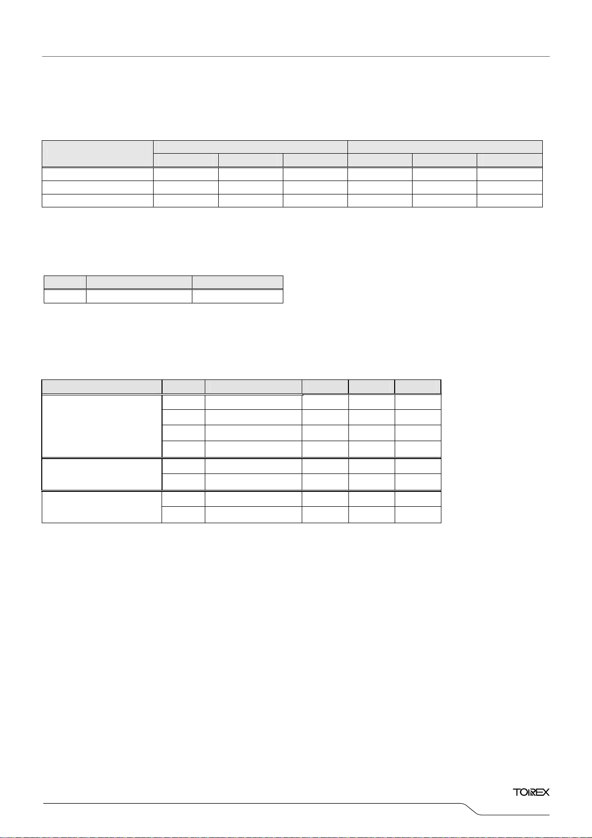
■ELECTRICAL CHARACTERISTICS (Continued)
●PFM Switching Current (I
(mA)
SETTING VOLTAGE
V
≦1.2V 140 180 240 190 260 350
OUT(E)
1.2V<V
1.8V≦V
≦1.75V 130 170 220 180 240 300
OUT(E)
120 160 200 170 220 270
OUT(E)
●Input Voltage (VIN) for Measuring Maximum PFM Switching Current (MAXI
f
1.2MHz 3.0MHz
OSC
(C-1) V
Minimum operating voltage is 2.7V.
ex.) Although when V
+0.5V V
OUT(E)
= 1.2V, f
OUT(E)
) by Oscillation Frequency and Setting Voltage
PFM
1.2MHz 3.0MHz
MIN. TYP. MAX. MIN. TYP. MAX.
+1.0V
OUT(E)
= 1.2MHz, (C-1) = 1.7V, the (C-1) becomes 2.7V because of the minimum operating voltage 2.7V.
OSC
PFM
XCM517
Series
) Limit
●Soft-start time by each setting voltage(XCM517Bx series only)
PRODUCT SERIES f
XC517BA
XC517BC
XC517BB
XC517BD
SETTING VOLTAGE MIN. TYP. MAX.
OSC
1.2MHz
1.2MHz
1.2MHz
1.2MHz
1.2MHz
1.2MHz
3.0MHz
3.0MHz
0.8V≦V
1.5V≦V
1.8V≦V
2.5V≦V
0.8V≦V
2.5V≦V
0.8V≦V
1.8V≦V
OUT(E)
OUT(E)
OUT(E)
OUT(E)
OUT(E)
OUT(E)
OUT(E)
OUT(E)
<1.5V
<1.8V
<2.5V
≦4.0V
<2.5V
≦4.0V
<1.8V
≦4.0V
-
-
-
-
-
-
-
-
250μs 400μs
320μs 500μs
250μs 400μs
320μs 500μs
250μs 400μs
320μs 500μs
250μs 400μs
320μs 500μs
9/28
 Loading...