

Torex XCL206B303-EVB, XCL206B283-EVB, XCL206B183-EVB, XCL206B153-EVB, XCL206B123-EVB User Manual

XCL206 Evaluation Board
‘micro-DC/DC’
Step-down DC/DC Converter with Integrated
Multilayer Inductor
USER MANUAL:
XCL206B123-EVB (V
OUT
= 1.2V)
XCL206B153-EVB (V
OUT
= 1.5V)
XCL206B183-EVB (V
OUT
= 1.8V)
XCL206B283-EVB (V
OUT
= 2.8V)
XCL206B303-EVB (V
OUT
= 3.0V)
ETR3101-D01a

WARNING
Torex Semiconductor does not guarantee that all samples will perform in exactly the same
way and we recommend that you always consult our product data sheets for the minimum
and maximum specifications.
XCL206 DATASHEET → www.torex.co.jp
It is also important that you evaluate all our products carefully before mass production and
in case of any doubt, please contact your Torex representative.
Important Notes:
・The operating temperature range for this IC is -20~+85℃.
・The operating DC input voltage range is from 2.0V to 6.0V.
If an input voltage higher than 6.0V is applied, the operation of this IC cannot be
guaranteed. Moreover, if a voltage higher than 6.5V is applied the IC may be permanently
damaged.
・At the output of the IC, if the selected load causes the IC to supply a continuous current
higher than the maximum rated current (600mA), the IC may be damaged.
XCL206 Evaluation Board
Inductor Built-in Step-Down DC/DC Converters
2
CAUTION
ENGINEERING EVALUATION PURPOSES ONLY
This evaluation board is made for the purpose of the XCL206 product evaluation.
It is strictly prohibited to use this evaluation board for any other purpose.

CONTENTS
1. INTRODUCTION …..………………………………………………………………...…………….4
2. QUICK START GUIDE…..………………………………………………………………………….5
2.1. CE pin (XCL206series).………….………………………….…………………………………5
3. SCHEMATIC, BOM AND PCB LAYOUT………………………………………………………….5
3.1. Schematic……...…………………………………………………………………………….....5
3.2. Bill of Materials...………………………...………………………………………………….....6
3.3. PCB layout ...…...…………………………………………………………………….……......7
4. TYPICAL CHARACTERISTICS…………………………………………………………….……8
4.1. XCL206B123-EVB...…………….…………………………………………………...………..8
4.2. XCL206B153-EVB……………….…………………………………...……….........…………9
4.3. XCL206B183-EVB...…………….…………………………………………………...………10
4.4. XCL206B283-EVB...…………….…………………………………………………...………11
4.5. XCL206B303-EVB...………………………………………………………………...……….12
XCL206 Evaluation Board
Inductor Built-in Step-Down DC/DC Converters
3
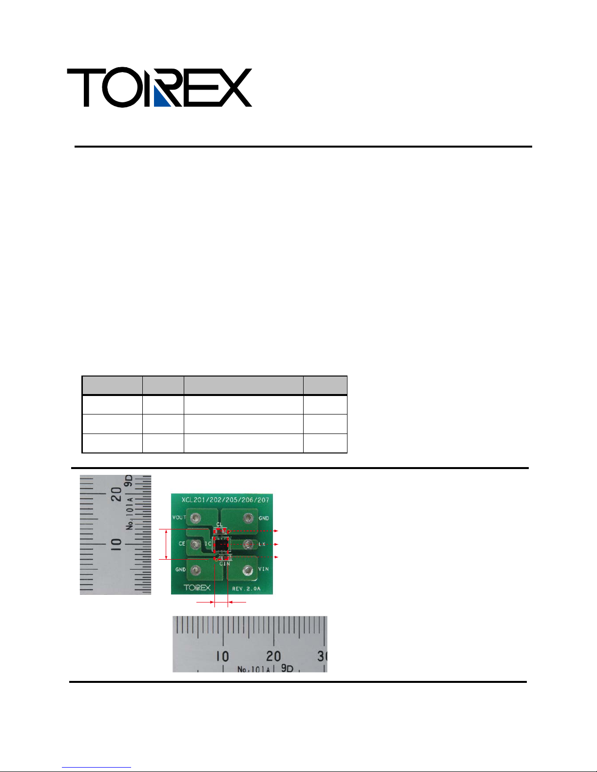
XCL206 Evaluation Board
Inductor Built-in Step-Down DC/DC Converters
The XCL206 series is a synchronous step-down DC/DC converter which integrates an inductor and a
control IC in one tiny package (2.5mm×2.0mm, H=1.0mm). A stable power supply with an output current of
600mA is configured using only two capacitors connected externally.
Operating voltage range is from 2.0V to 6.0V. Output voltage is internally set in a range from 0.8V to 4.0V in
increments of 0.05V. The device is operated by 3.0MHz, and includes 0.42ΩP-channel driver transistor
and 0.52ΩN-channel switching transistor. The XCL206 series has automatic PWM/PFM switching control,
allowing fast response, low ripple and high efficiency over the full range of loads (from light load to heavy
load). During stand-by, the device is shutdown to reduce current consumption to as low as 1.0μA or less.
With the built-in UVLO (Under Voltage Lock Out) function, the internal driver transistor is forced OFF when
input voltage becomes 1.4Vor lower. XCL206B series provide short-time turn-on by the soft start function
internally set in 0.25ms (TYP). XCL206B integrate CL auto discharge function which enables the electric
charge stored at the output capacitor CL to be discharged via the internal auto-discharge switch located
between the LX and VSS pins. When the devices enter stand-by mode, output voltage quickly returns to the
V
SS
level as a result of this function.
Chapter 1: INTRODUCTION
4
2.5mm
6.0mm
Capacitor
IC
Capacitor
Parameter Symbol Value Unit
Input Voltage
V
IN
~ 6.0 V
Output Voltage
V
OUT
1.2V, 1.5V, 1.8V, 2.8V, 3.0V V
Output Current
I
OUT
600 mA
 Loading...