

TOREX XCL205, XCL206, XCL207 User Manual
1/26
XCL205/XCL206/XCL207
Series
Inductor Built-in Step-Down “micro DC/DC” Converters
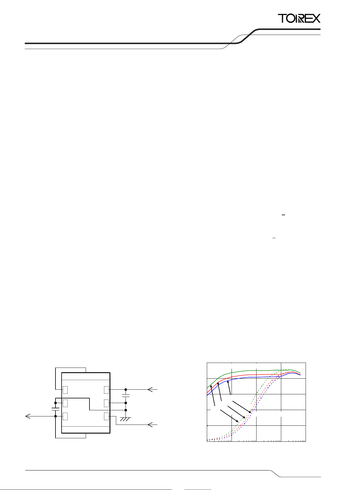
0
20
40
60
80
100
0.1 1 10 100 1000
Output Current:I
OUT
(mA)
Efficency:EFFI(%
)
VIN= 5.5V
5.0V
4.2V
VOUT=3.3V
(
PWM
)
XCL206/XCL207(PWM/PFM
)
XCL205/XCL207
!TYPICAL PERFORMANCE
CHARACTERISTICS
"GreenOperation Compatible
!APPLICATIONS
#Mobile phones, Smart phones
#Bluetooth Headsets
#WiMAX PDAs, MIDs, UMPCs
#Portable game consoles
#Digital cameras, Camcorders
#Electronic dictionaries
!TYPICAL APPLICATION CIRCUIT
ETR2801-006
!GENERAL DESCRIPTION
The XCL205/XCL206/XCL207 series is a synchronous step-down micro DC/DC converter which integrates an inductor and a
control IC in one tiny package (2.5mm$2.0mm, H=1.0mm). A stable power supply with an output current of 600mA is
configured using only two capacitors connected externally.
Operating voltage range is from 2.0V to 6.0V. Output voltage is internally set in a range from 0.8V to 4.0V in increments of
0.05V. The device is operated by 3.0MHz, and includes 0.42%P-channel driver transistor and 0.52%N-channel switching
transistor. As for operation mode, the XCL205 series is PWM control, the XCL206 series is automatic PWM/PFM switching
control and the XCL207 series can be manually switched between the PWM control mode and the automatic PWM/PFM
switching control mode, allowing fast response, low ripple and high efficiency over the full range of loads (from light load to
heavy load). During stand-by, the device is shutdown to reduce current consumption to as low as 1.0&A or less. With the
built-in UVLO (Under Voltage Lock Out) function, the internal driver transistor is forced OFF when input voltage becomes 1.4V
or lower. XCL205B/XCL206B/XCL207B series provide short-time turn-on by the soft start function internally set in 0.25 ms
(TYP). XCL205B(C) /XCL206 B(C) / XCL207B(C) integrate C
L
auto discharge function which enables the electric charge
stored at the output capacitor C
L
to be discharged via the internal auto-discharge switch located between the LX and VSS pins.
When the devices enter stand-by mode, output voltage quickly returns to the V
SS
level as a result of this function.
V
IN
Vss
CE/MODE
L
X
V
ss
V
OUT
CL
10&F
4.7&F
CIN
L1
L2
600mA
(TOP VIEW)
* “L1 and L
X
”, and “L2 and V
OUT
” is connected by wiring.
!FEATURES
Ultra Small : 2.5mm$2.0mm, H=1.0mm
Input Voltage : 2.0V ~ 6.0V
Output Voltage : 0.8V ~ 4.0V (+2.0%)
High Efficiency (V
OUT
=1.8V) : 85% (TYP.)
Output Current : 600mA
Oscillation Frequency : 3.0MHz (+15%)
Maximum Duty Cycle
Capacitor
CE Function
Protection Circuits
: 100%
: Low ESR Ceramic
: Active High
Soft-Start Circuit Built-In
C
L
High Speed Auto Discharge
:Current Limiter Circuit Built-In
(Constant Current & Latching)
Control Methods : PWM (XCL205)
PWM/PFM Auto (XCL206)
PWM/PFM Manual (XCL207)
* Performance depends on external components and wiring on the PCB.
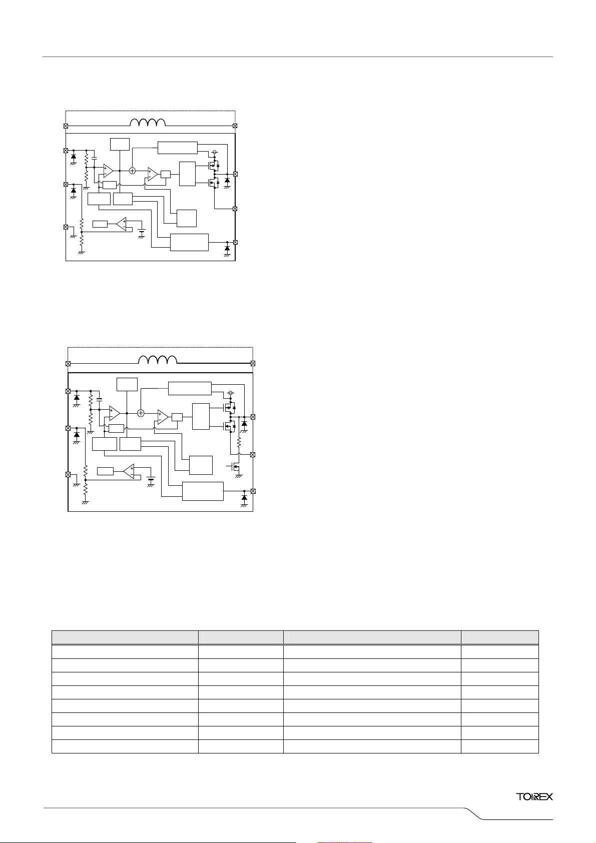
XCL205A333xx/XCL206A333xx/XCL207A333xx
XCL205/206/207 Series

PIN NUMBER PIN NAME
FUNCTION
1 Lx Switching Output
2,5 VSS Ground
3 V
OUT
Output Voltage
4 CE / MODE Chip Enable & Mode Switch
6 VIN Power Input
7 L1
8 L2
Inductor Electrodes
DESIGNATOR DESCRIPTION SYMBOL DESCRIPTION
A
No CL auto discharge, Standard soft-start
B
CL auto discharge, High speed soft-start
'
Functions selection
(All CE active high)
C
C
L
auto discharge, Standard soft-start
10 1.0V
12 1.2V
14 1.4V
15 1.5V
18 1.8V
19 1.9V
25 2.5V
28 2.8V
2L 2.85V
30 3.0V
()
Output Voltage
(*2)
33 3.3V
* Oscillation Frequency
3 3.0MHz
+,--
Packages
Taping Type
(*3)
AR-G XCL205/6/7
!"##"$ %&'()
*+
*,
-
.
%
&/
0
%
11
2
3'4$"5'
6
+
*7
, % 11
8 %
"9#
* It should be connected the V
SS pin (No. 2 and 5) to the GND pin.
* If the dissipation pad needs to be connected to other pins, it should be
connected to the GND pin.
* Please refer to pattern layout page for the connecting to PCB.
(*1)
The “-G” suffix indicates that the products are Halogen and Antimony free as well as being fully RoHS compliant.
(*2)
When other output voltages are needed, please contact your local Torex sales office for more information.
Output voltage range is 0.8~4.0V.
(*3)
The device orientation is fixed in its embossed tape pocket.
XCL205/XCL206/XCL207
Series
!PIN CONFIGURATION
!PIN ASSIGNMENT
!PRODUCT CLASSIFICATION
#Ordering Information
XCL205'()*+,-XCL206'()*+,-XCL207'()*+,--
(*1)
Fixed PWM control
(*1)
PWM / PFM automatic switching control
(*1)
Manual Mode Selection Pin (Semi-custom)
2/26
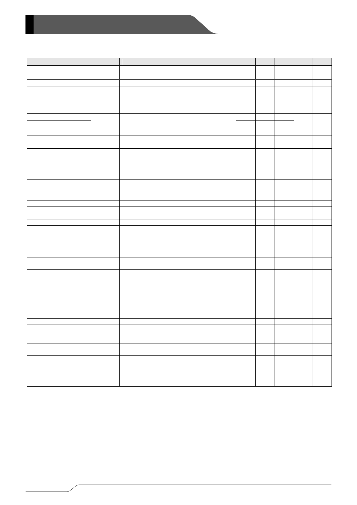
PARAMETER SYMBOL RATINGS UNITS
VIN Pin Voltage VIN - 0.3 ~ 6.5 V
LX Pin Voltage VLX - 0.3 ~ VIN + 0.3/6.5 V
V
OUT
Pin Voltage V
OUT
- 0.3 ~ 6.5 V
CE/MODE Pin Voltage VCE - 0.3 ~ 6.5 V
LX Pin Current ILX 01500 mA
Power Dissipation Pd 1000*1 mW
Operating Temperature Range Topr - 40 ~ + 85 .
Storage Temperature Range Tstg - 40 ~ + 105 .
#XCL205A / XCL206A / XCL207A series
NOTE: The XCL205 offers a fixed PWM control, a signal from CE/MODE Control Logic to PWM/PFM Selector is fixed to "L" level inside.
The XCL206 control scheme is PWM/PFM automatic switching, a signal from CE/MODE Control Logic to PWM/PFM Selector is fixed to
"H" level inside. The diodes placed inside are ESD protection diodes and parasitic diodes.
3'4$"5'
:,
:+
';;<;=>?@A
%;BC=DEFG
H<CF=HFI;FJ
3'
KGI1B
3<?@BL1IFE<L
K($4KM$
HBNBOF<;
3P;;BLF=MBBQRIOS
3P;;BLF=*E?EF
K($
3<?@I;IF<;
*<TEO
HULOG
!PCCB;
5;EVB
:8
:6
9%*"
9%*"=3?@
:I?@=(IVB
WBLB;IF<;
"H3
*7
%
HH
%&/
%"9#
3'4$"5'
3<LF;<N
*<TEO
%HX":#
M!
3M!
&LQPOF<;
%HH
*, *+
*1: The power dissipation figure shown is PCB mounted (40mm$40mm, t=1.6mm, Glass Epoxy FR-4).
Please refer to page 16 for details.
#XCL205B / XCL206B / XCL207B / XCL205C / XCL206C / XCL207C series
3'4$"5'
:,
:+
';;<;=>?@A
%;BC=DEFG
H<CF=HFI;FJ
3'
KGI1B
3<?@BL1IFE<L
K($4KM$
HBNBOF<;
3P;;BLF=MBBQRIOS
3P;;BLF=*E?EF
K($
3<?@I;IF<;
*<TEO
HULOG
!PCCB;
5;EVB
:8
:6
9%*"
9%*"=3?@
:I?@=(IVB
WBLB;IF<;
"H3
*7
%HH
%&/
%"9#
3'4$"5'
3<LF;<N
*<TEO
3'4
%HX":#
M!
3M!
%HH
&LQPOF<;
*, *+
NOTE: The XCL205 offers a fixed PWM control, a signal from CE/MODE Control Logic to PWM/PFM Selector is fixed to "L" level inside.
The XCL206 control scheme is PWM/PFM automatic switching, a signal from CE/MODE Control Logic to PWM/PFM Selector is fixed to
"H" level inside. The diodes placed inside are ESD protection diodes and parasitic diodes.
XCL205/XCL206/XCL207
!BLOCK DIAGRAM
Series
!ABSOLUTE MAXIMUM RATINGS
Ta = 25.
3/26
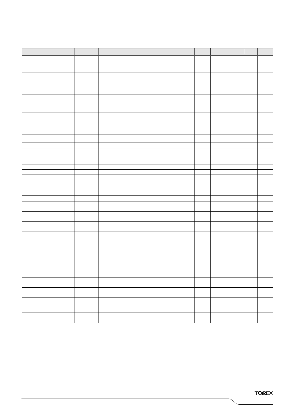
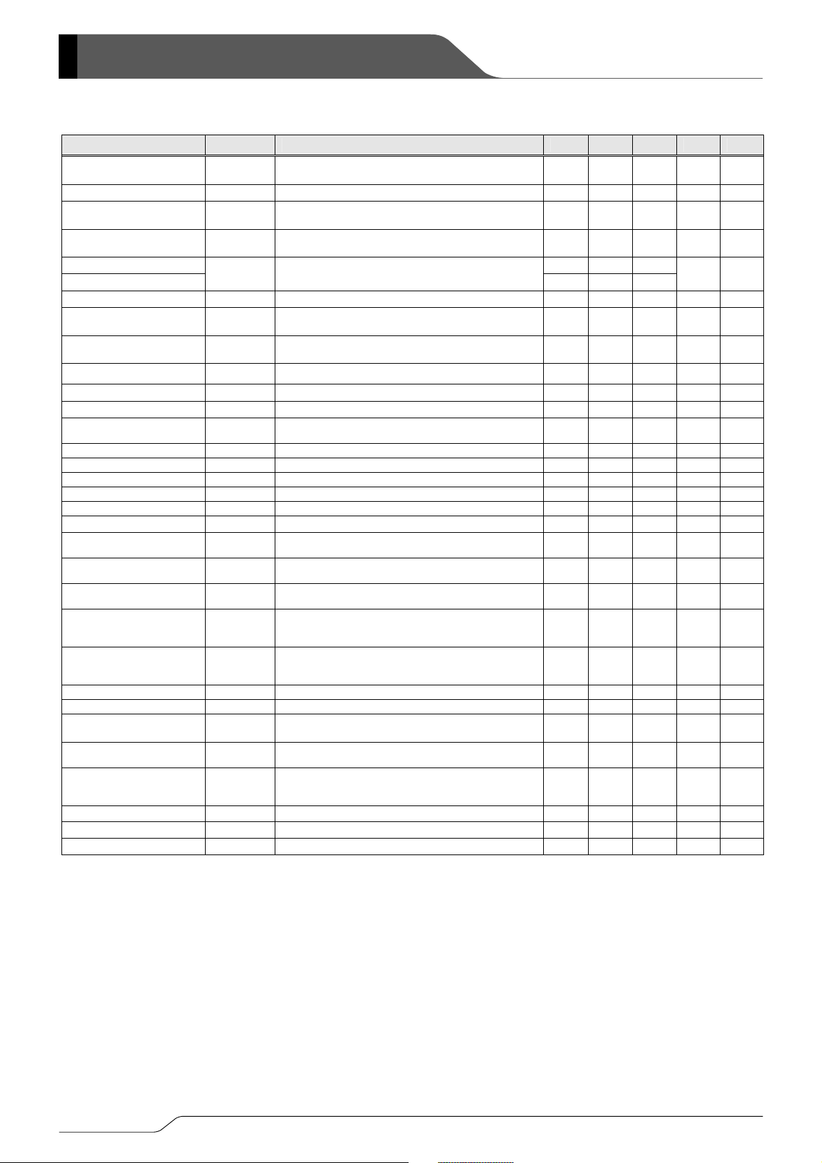
PARAMETER SYMBOL CONDITIONS MIN. TYP. MAX. UNITS
CIRCUIT
Output Voltage V
OUT
When connected to external components,
V
IN=VCE
=5.0V, I
OUT
=30mA
1.176 1.200 1.224 V '
Operating Voltage Range VIN 2.0 - 6.0 V '
Maximum Output Current I
OUTMAX
V
IN=VOUT(T)
+2.0V, VCE=1.0V
When connected to external components
(*9)
600 - - mA '
UVLO Voltage V
UVLO
V
CE=VIN,VOUT
=0V,
Voltage which Lx pin holding “L” level
(*1, *11)
1.00 1.40 1.78 V )
Supply Current (XCL205) - 46 65
Supply Current (XCL206, XCL207)
IDD VIN=VCE=5.0V, V
OUT=VOUT(T)
$1.1V
- 21 35
&A (
Stand-by Current I
STB
VIN=5.0V, VCE=0V, V
OUT=VOUT(T)
$1.1V - 0 1.0 &A (
Oscillation Frequency f
OSC
When connected to external components,
V
IN=VOUT(T)
+2.0V,VCE=1.0V, I
OUT
=100mA
2550 3000 3450 kHz '
PFM Switching Current
(*12)
I
PFM
When connected to external components,
V
IN=VOUT(T)
+2.0V, VCE=VIN , I
OUT
=1mA
(*12)
190 260 350 mA 1
PFM Duty Limit
(*12)
DTY
LIMIT_PFM
V
CE
= VIN=(C-1) I
OUT
=1mA
(*12)
- 200 300 % '
Maximum Duty Cycle
D
MAX
V
IN=VCE
=5.0V, V
OUT=VOUT (T)
$0.9V 100 - - % )
Minimum Duty Cycle
D
MIN
V
IN=VCE
=5.0V, V
OUT=VOUT (T)
$1.1V - - 0 % )
Efficiency
EFFI
When connected to external components,
V
CE=VIN2VOUT (T)
+1.2V, I
OUT
= 100mA
- 82 - % '
Lx SW "H" ON Resistance 1 R
L3H
VIN=VCE=5.0V, V
OUT
=0V, ILX=100mA
(*3)
- 0.35 0.55 % *
Lx SW "H" ON Resistance 2 R
L3H
VIN=VCE=3.6V, V
OUT
=0V, ILX=100mA
(*3)
- 0.42 0.67 % *
Lx SW "L" ON Resistance 1 R
L3L
VIN=VCE=5.0V
(*4)
- 0.45 0.66 % -
Lx SW "L" ON Resistance 2 R
L3L
VIN=VCE=3.6V,
(*4)
- 0.52 0.77 % -
Lx SW "H" Leak Current
(*5)
ILeakH VIN=V
OUT
=5.0V, VCE=0V, LX=0V - 0.01 1.0 &A +
Lx SW "L" Leak Current
(*5)
ILeakL VIN=V
OUT
=5.0V, VCE=0V, LX= 5.0V - 0.01 1.0 &A +
Current Limit
(*10)
I
LIM
VIN=VCE=5.0V, V
OUT=VOUT (E)
$0.9V
(*8)
900 1050 1350 mA ,
Output Voltage
Temperature Characteristics
4
V
OUT
/
(V
OUT
54
topr)
I
OUT
=30mA
-40./Topr/85.
- 0100 - ppm/ . '
CE "H" Voltage V
CEH
V
OUT
=0V, Applied voltage to VCE,
Voltage changes Lx to “H” level
(*11)
0.65 - V
IN
V )
CE "L" Voltage V
CEL
V
OUT
=0V, Applied voltage to VCE,
Voltage changes Lx to “L” level
(*11)
V
SS
- 0.25 V )
PWM "H" Level Voltage
(*13)
V
PWMH
When connected to external components,
I
OUT
=1mA
(*6),
Voltage which oscillation
frequency becomes 2550kHz/f
OSC
/3450kHz
(*13)
- - VIN - 1.0 V '
PWM "L" Level Voltage
(*13)
V
PWML
When connected to external components,
I
OUT
=1mA
(*6)
, Voltage which oscillation
frequency becomes f
OSC
62550kHz
(*13)
V
IN
-
0.25
- - V '
CE "H" Current I
CEH
VIN=VCE=5.0V, V
OUT
=0V - 0.1 - 0.1 &A +
CE "L" Current I
CEL
VIN=5.0V, VCE=0V, V
OUT
=0V - 0.1 - 0.1 &A +
Soft Start Time tSS
When connected to external components,
V
CE
=0V7VIN , I
OUT
=1mA
0.5 0.9 2.5 ms '
Latch Time t
LAT
V
IN
=
VCE=5.0V,
V
OUT
=0.8$V
OUT
(T)
Short Lx at 1% resistance
(*7)
1.0 - 20 ms -
Short Protection
Threshold Voltage
V
SHORT
Sweeping V
OUT
, VIN=VCE=5.0V, Short Lx at
1% resistance, V
OUT
voltage which Lx becomes “L”
level within 1ms
0.450 0.600 0.750 V -
Inductance Value L Test frequency=1MHz - 1.5 - &H
Allowed Inductor Current IDC 8T=40. - 1000 - mA
Test conditions: Unless otherwise stated, VIN=5.0V, VOUT (T)=Nominal Voltage
NOTE:
*1: Including hysteresis operating voltage range.
*2: EFFI = { ( output voltage$output current ) 9 ( input voltage$input current) }$100
*3: ON resistance (%)= (V
IN - Lx pin measurement voltage) 9 100mA
*4: Design value
*5: When temperature is high, a current of approximately 10&A (maximum) may leak.
*6: The CE/MODE pin of the XCL207 series works also as an external switching pin of PWM control and PWM/PFM control. When the IC is in the
operation, control is switched to the automatic PWM/PFM switching mode when the CE/MODE pin voltage is equal to or greater than V
IN minus
0.3V, and to the PWM mode when the CE/MODE pin voltage is equal to or lower than V
IN minus 1.0V and equal to or greater than VCEH.
*7: Time until it short-circuits V
OUT with GND via 1%of resistor from an operational state and is set to Lx=0V from current limit pulse generating.
*8: When V
IN is less than 2.4V, limit current may not be reached because voltage falls caused by ON resistance.
*9: When the difference between the input and the output is small, some cycles may be skipped completely before current maximizes.
If current is further pulled from this state, output voltage will decrease because of P-ch driver ON resistance.
*10: Current limit denotes the level of detection at peak of coil current.
*11: “H”=V
IN~VIN-1.2V, “L”=+0.1V~-0.1V
*12: I
PFM and DTY
LIMIT_PFM
are defined only for the XCL206 and XCL207 series which have PFM control function. (Not for the XCL 205 series)
*13: V
PWMH and VPWML are defined onl
y
for the XCL207 series. (They are not used in the XCL205/and XCL206 series)
XCL205/XCL206/XCL207
Series
!ELECTRICAL CHARACTERISTICS
#XCL205A123AR/XCL206A123AR/XCL207A123AR, V
OUT
=1.2V, f
4/26
=3.0MHz, Ta=25Y=
OSC
PARAMETER SYMBOL CONDITIONS MIN. TYP. MAX. UNITS
CIRCUIT
Output Voltage V
OUT
When connected to external components,
V
IN=VCE
=5.0V, I
OUT
=30mA
1.764 1.800 1.836 V '
Operating Voltage Range VIN 2.0 - 6.0 V '
Maximum Output Current I
OUTMAX
V
IN=VOUT(E)
+2.0V, VCE=1.0V
When connected to external components
(*9)
600 - - mA '
UVLO Voltage V
UVLO
V
CE=VIN,VOUT
=0V,
Voltage which Lx pin holding “L” level
(*1, *11)
1.00 1.40 1.78 V )
Supply Current (XCL205) - 46 65
Supply Current (XCL206, XCL207)
I
DD
VIN=VCE=5.0V, V
OUT=VOUT(T)
$1.1V
- 21 35
&A (
Stand-by Current I
STB
VIN=5.0V, VCE=0V, V
OUT=VOUT(T)
$1.1V - 0 1.0 &A (
Oscillation Frequency f
OSC
When connected to external components,
V
IN=VOUT(T)
+2.0V,VCE=1.0V, I
OUT
=100mA
2550 3000 3450 kHz '
PFM Switching Current
(*12)
I
PFM
When connected to external components,
V
IN=VOUT(T)
+2.0V, VCE=VIN , I
OUT
=1mA
(*12)
170 220 270 mA 1
PFM Duty Limit
(*12)
DTY
LIMIT_PFM
V
CE
= VIN=(C-1) I
OUT
=1mA
(*12)
- 200 300 % '
Maximum Duty Cycle D
MAX
VIN=VCE=5.0V, V
OUT=VOUT (T)
$0.9V 100 - - % )
Minimum Duty Cycle D
MIN
VIN=VCE=5.0V, V
OUT=VOUT (T)
$1.1V - - 0 % )
Efficiency EFFI
When connected to external components,
V
CE=VIN2VOUT (T)
+1.2V, I
OUT
= 100mA
- 85 - % '
Lx SW "H" ON Resistance 1 R
L3H
VIN=VCE=5.0V, V
OUT
=0V, ILX=100mA
(*3)
- 0.35 0.55 % *
Lx SW "H" ON Resistance 2 R
L3H
VIN=VCE=3.6V, V
OUT
=0V, ILX=100mA
(*3)
- 0.42 0.67 % *
Lx SW "L" ON Resistance 1 R
L3L
VIN=VCE=5.0V
(*4)
- 0.45 0.66 % -
Lx SW "L" ON Resistance 2 R
L3L
VIN=VCE=3.6V,
(*4)
- 0.52 0.77 % -
Lx SW "H" Leak Current
(*5)
ILeakH VIN=V
OUT
=5.0V, VCE=0V, LX=0V - 0.01 1.0 &A +
Lx SW "L" Leak Current
(*5)
ILeakL VIN=V
OUT
=5.0V, VCE=0V, LX= 5.0V - 0.01 1.0 &A +
Current Limit
(*10)
I
LIM
VIN=VCE=5.0V, V
OUT=VOUT (E)
$0.9V
(*8)
900 1050 1350 mA ,
Output Voltage
Temperature Characteristics
4
V
OUT
/
(V
OUT
54
topr)
I
OUT
=30mA
-40./Topr/85.
- 0100 - ppm/ . '
CE "H" Voltage V
CEH
V
OUT
=0V, Applied voltage to VCE,
Voltage changes Lx to “H” level
(*11)
0.65 - V
IN
V )
CE "L" Voltage V
CEL
V
OUT
=0V, Applied voltage to VCE,
Voltage changes Lx to “L” level
(*11)
V
SS
- 0.25 V )
PWM "H" Level Voltage
(*13)
V
PWMH
When connected to external components,
I
OUT
=1mA
(*6),
Voltage which oscillation
frequency becomes 2550kHz/f
OSC
/3450kHz
(*13)
- - VIN - 1.0 V '
PWM "L" Level Voltage
(*13)
V
PWML
When connected to external components,
I
OUT
=1mA
(*6)
, Voltage which oscillation
frequency becomes f
OSC
62550kHz
(*13)
V
IN
-
0.25
- - V '
CE "H" Current I
CEH
VIN=VCE=5.0V, V
OUT
=0V - 0.1 - 0.1 &A +
CE "L" Current I
CEL
VIN=5.0V, VCE=0V, V
OUT
=0V - 0.1 - 0.1 &A +
Soft Start Time tSS
When connected to external components,
V
CE
=0V7VIN , I
OUT
=1mA
0.5 0.9 2.5 ms '
Latch Time t
LAT
V
IN
=
VCE=5.0V,
V
OUT
=0.8$V
OUT
(T)
Short Lx at 1% resistance
(*7)
1.0 - 20 ms -
Short Protection
Threshold Voltage
V
SHORT
Sweeping V
OUT
, VIN=VCE=5.0V, Short Lx at
1% resistance, V
OUT
voltage which Lx becomes “L”
level within 1ms
0.675 0.900 1.125 V -
Inductance Value L Test frequency =1MHz - 1.5 - &H
Allowed Inductor Current IDC 8T=40. - 1000 - mA
Test conditions: Unless otherwise stated, VIN=5.0V, VOUT (T)=Nominal Voltage
NOTE:
*1: Including hysteresis operating voltage range.
*2: EFFI = { ( output voltage$output current ) 9 ( input voltage$input current) }$100
*3: ON resistance (%)= (V
IN - Lx pin measurement voltage) 9 100mA
*4: Design value
*5: When temperature is high, a current of approximately 10&A (maximum) may leak.
*6: The CE/MODE pin of the XCL207 series works also as an external switching pin of PWM control and PWM/PFM control. When the IC is in the
operation, control is switched to the automatic PWM/PFM switching mode when the CE/MODE pin voltage is equal to or greater than V
IN minus
0.3V, and to the PWM mode when the CE/MODE pin voltage is equal to or lower than V
IN minus 1.0V and equal to or greater than VCEH.
*7: Time until it short-circuits V
OUT with GND via 1%of resistor from an operational state and is set to Lx=0V from current limit pulse generating.
*8: When V
IN is less than 2.4V, limit current may not be reached because voltage falls caused by ON resistance.
*9: When the difference between the input and the output is small, some cycles may be skipped completely before current maximizes.
If current is further pulled from this state, output voltage will decrease because of P-ch driver ON resistance.
*10: Current limit denotes the level of detection at peak of coil current.
*11: “H”=V
IN~VIN-1.2V, “L”=+0.1V~-0.1V
*12:
IPFM and DTY
LIMIT_PFM
are defined only for the XCL206 and XCL207 series which have PFM control function. (Not for the XCL 205 series)
*13: V
PWMH and VPWML are defined only for the XCL207 series. (They are not used in the XCL205/and XCL206 series)
!ELECTRICAL CHARACTERISTICS (Continued)
#XCL205A183AR/XCL206A183AR/XCL207A183AR, V
OUT
=1.8V, f
=3.0MHz, Ta=25Y=
OSC
XCL205/XCL206/XCL207
Series
5/26
PARAMETER SYMBOL CONDITIONS MIN. TYP. MAX. UNITS
CIRCUIT
Output Voltage
V
OUT
When connected to external components,
V
IN=VCE
=5.0V, I
OUT
=30mA
1.176 1.200 1.224 V '
Operating Voltage Range
V
IN
2.0 - 6.0 V '
Maximum Output Current
I
OUTMAX
V
IN=VOUT(T)
+2.0V, VCE=1.0V
When connected to external components
(*9)
600 - - mA '
UVLO Voltage
V
UVLO
V
CE=VIN,VOUT
=0V,
Voltage which Lx pin holding “L” level
(*1, *11)
1.00 1.40 1.78 V )
Supply Current (XCL205) - 46 65
Supply Current (XCL206, XCL207)
I
DD
VIN=VCE=5.0V, V
OUT=VOUT(T)
$1.1V
- 21 35
&A (
Stand-by Current
I
STB
V
IN
=5.0V, VCE=0V, V
OUT=VOUT(T)
$1.1V
- 0 1.0 &A (
Oscillation Frequency
f
OSC
When connected to external components,
V
IN
=V
OUT(T)
+2.0V,VCE=1.0V, I
OUT
=100mA
2550 3000 3450 kHz '
PFM Switching Current
(*12)
I
PFM
When connected to external components,
V
IN
=V
OUT(T)
+2.0V, VCE = VIN , I
OUT
=1mA
(*12)
190 260 350 mA 1
PFM Duty Limit
(*12)
DTY
LIMIT_PFM
V
CE=VIN
=(C-1) I
OUT
=1mA
(*12)
- 200 300 % '
Maximum Duty Cycle D
MAX
VIN=VCE=5.0V, V
OUT=VOUT (T)
$0.9V
100 - - % )
Minimum Duty Cycle D
MIN
V
IN=VCE
=5.0V, V
OUT=VOUT (T)
$1.1V
- - 0 % )
Efficiency
EFFI
When connected to external components,
V
CE=VIN2VOUT (T)
+1.2V, I
OUT
=100mA
- 82 - % '
Lx SW "H" ON Resistance 1
R
L3H
VIN=VCE=5.0V, V
OUT
=0V, ILX=100mA
(*3)
- 0.35 0.55 % *
Lx SW "H" ON Resistance 2
R
L3H
VIN=VCE=3.6V, V
OUT
=0V, ILX=100mA
(*3)
- 0.42 0.67 % *
Lx SW "L" ON Resistance 1
R
L3L
V
IN=VCE
=5.0V
(*4)
- 0.45 0.66 % -
Lx SW "L" ON Resistance 2
R
L3L
V
IN=VCE
= 3.6V
(*4)
- 0.52 0.77 % -
Lx SW "H" Leak Current
(*5)
ILeakH
VIN=V
OUT
=5.0V, VCE =0V, LX=0V
- 0.01 1.0 &A :
Current Limit
(*10)
I
LIM
V
IN=VCE
=5.0V, V
OUT=VOUT (T)
$0.9V
(*8)
900 1050 1350 mA ,
Output Voltage
Temperature Characteristics
4
V
OUT
/
(V
OUT
54
topr)
I
OUT
=30mA
-40./Topr/85.
- 0100 - ppm/ . '
CE "H" Voltage
V
CEH
V
OUT
=0V, Applied voltage to VCE,
Voltage changes Lx to “H” level
(*11)
0.65 - V
IN
V )
CE "L" Voltage
V
CEL
V
OUT
=0V, Applied voltage to VCE,
Voltage changes Lx to “L” level
(*11)
V
SS
- 0.25 V )
PWM "H" Level Voltage
(*13)
V
PWMH
When connected to external components,
I
OUT
=1mA
(*6),
Voltage which oscillation
frequency becomes 2550kHz/f
OSC
/3450kHz
(*13)
- - VIN - 1.0 V '
PWM "L" Level Voltage
(*13)
V
PWML
When connected to external components,
I
OUT
=1mA
(*6)
, Voltage which oscillation
frequency becomes f
OSC
62550kHz
(*13)
V
IN
-
0.25
- - V '
CE "H" Current
I
CEH
VIN=VCE=5.0V, V
OUT
=0V
- 0.1 - 0.1 &A +
CE "L" Current
I
CEL
VIN=5.0V, VCE=0V, V
OUT
=0V
- 0.1 - 0.1 &A +
Soft Start Time
t
SS
When connected to external components,
V
CE
=0V7VIN , I
OUT
=1mA
- 0.25 0.40 ms '
Latch Time
t
LAT
V
IN=VCE
=5.0V, V
OUT
=0.8$V
OUT(T)
Short Lx at 1% resistance
(*7)
1.0 - 20 ms -
Short Protection
Threshold Voltage
V
SHORT
Sweeping V
OUT
, VIN=VCE=5.0V, Short Lx at
1% resistance, V
OUT
voltage which Lx becomes “L”
level within 1ms
0.450 0.600 0.750 V -
CL Discharge
R
DCHG
V
IN
=5.0V, LX=5.0V, VCE=0V, V
OUT
=Open
200 300 450 % ;
Inductance Value
L
Test frequency =1MHz
- 1.5 - &H
Allowed Inductor Current IDC
8T=40.
- 1000 - mA
Test conditions: Unless otherwise stated, VIN=5.0V, VOUT (T) =Nominal Voltage
NOTE:
*1: Including hysteresis operating voltage range.
*2: EFFI = { ( output voltage$output current ) 9 ( input voltage$input current) }$100
*3: ON resistance (%)= (V
IN - Lx pin measurement voltage) 9 100mA
*4: Design value
*5: When temperature is high, a current of approximately 10&A (maximum) may leak.
*6: The CE/MODE pin of the XCL207 series works also as an external switching pin of PWM control and PWM/PFM control. When the IC is in the
operation, control is switched to the automatic PWM/PFM switching mode when the CE/MODE pin voltage is equal to or greater than V
IN minus
0.3V, and to the PWM mode when the CE/MODE pin voltage is equal to or lower than V
IN minus 1.0V and equal to or greater than VCEH.
*7: Time until it short-circuits V
OUT with GND via 1%of resistor from an operational state and is set to Lx=0V from current limit pulse generating.
*8: When V
IN is less than 2.4V, limit current may not be reached because voltage falls caused by ON resistance.
*9: When the difference between the input and the output is small, some cycles may be skipped completely before current maximizes.
If current is further pulled from this state, output voltage will decrease because of P-ch driver ON resistance.
*10: Current limit denotes the level of detection at peak of coil current.
*11: “H”=V
IN~VIN-1.2V, “L”=+0.1V~-0.1V
*12: I
PFM and DTY
LIMIT_PFM
are defined only for the XCL206 and XCL207 series which have PFM control function. (Not for the XCL 205 series)
*13: V
PWMH and VPWML are defined only for the XCL207 series. (They are not used in the XCL205/and XCL206 series)
XCL205/XCL206/XCL207
Series
!ELECTRICAL CHARACTERISTICS (Continued)
#XCL205B123AR/XCL206B123AR/ XCL207B123AR, V
OUT
=1.2V, f
=3.0MHz, Ta=25Y=
OSC
6/26
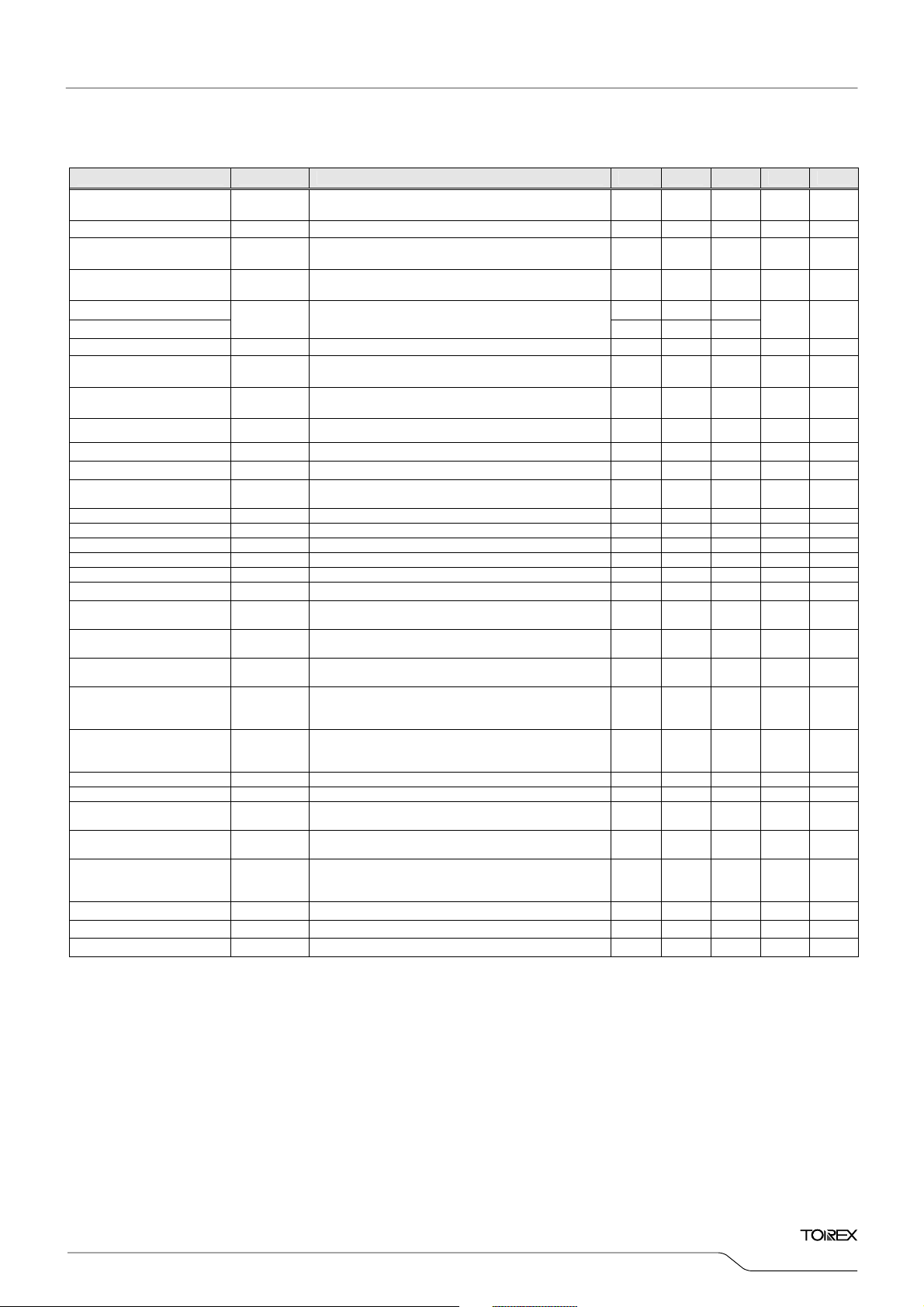
PARAMETER SYMBOL CONDITIONS MIN. TYP. MAX. UNITS
CIRCUIT
Output Voltage V
OUT
When connected to external components,
V
IN=VCE
=5.0V, I
OUT
=30mA
1.764 1.800 1.836 V '
Operating Voltage Range VIN 2.0 - 6.0 V '
Maximum Output Current I
OUTMAX
V
IN=VOUT(E)
+2.0V, VCE=1.0V
When connected to external components
(*9)
600 - - mA '
UVLO Voltage V
UVLO
V
CE=VIN,VOUT
=0V,
Voltage which Lx pin holding “L” level
(*1, *11)
1.00 1.40 1.78 V )
Supply Current (XCL205) - 46 65
Supply Current (XCL206, XCL207)
I
DD
VIN=VCE=5.0V, V
OUT=VOUT(T)
$1.1V
- 21 35
&A (
Stand-by Current I
STB
VIN=5.0V, VCE=0V, V
OUT=VOUT(T)
$1.1V - 0 1.0 &A (
Oscillation Frequency f
OSC
When connected to external components,
V
IN
=V
OUT(T)
+2.0V,VCE=1.0V, I
OUT
=100mA
2550 3000 3450 kHz '
PFM Switching Current
(*12)
I
PFM
When connected to external components,
V
IN
=V
OUT(T)
+2.0V, VCE = VIN , I
OUT
=1mA
(*12)
170 220 270 mA 1
PFM Duty Limit
(*12)
DTY
LIMIT_PFM
V
CE=VIN
=(C-1) I
OUT
=1mA
(*12)
- 200 300 % '
Maximum Duty Cycle D
MAX
VIN=VCE=5.0V, V
OUT=VOUT (T)
$0.9V 100 - - % )
Minimum Duty Cycle D
MIN
VIN=VCE=5.0V, V
OUT=VOUT (T)
$1.1V - - 0 % )
Efficiency EFFI
When connected to external components,
V
CE=VIN2VOUT (T)
+1.2V, I
OUT
=100mA
- 85 - % '
Lx SW "H" ON Resistance 1 R
L3H
VIN=VCE=5.0V, V
OUT
=0V, ILX=100mA
(*3)
- 0.35 0.55 % *
Lx SW "H" ON Resistance 2 R
L3H
VIN=VCE=3.6V, V
OUT
=0V, ILX=100mA
(*3)
- 0.42 0.67 % *
Lx SW "L" ON Resistance 1 R
L3L
VIN=VCE=5.0V
(*4)
- 0.45 0.66 % -
Lx SW "L" ON Resistance 2 R
L3L
VIN=VCE = 3.6V
(*4)
- 0.52 0.77 % -
Lx SW "H" Leak Current
(*5)
ILeakH VIN=V
OUT
=5.0V, VCE =0V, LX=0V - 0.01 1.0 &A :
Current Limit
(*10)
I
LIM
VIN=VCE=5.0V, V
OUT=VOUT (T)
$0.9V
(*8)
900 1050 1350 mA ,
Output Voltage
Temperature Characteristics
4
V
OUT
/
(V
OUT
54
topr)
I
OUT
=30mA
-40./Topr/85.
- 0100 - ppm/ . '
CE "H" Voltage V
CEH
V
OUT
=0V, Applied voltage to VCE,
Voltage changes Lx to “H” level
(*11)
0.65 - V
IN
V )
CE "L" Voltage V
CEL
V
OUT
=0V, Applied voltage to VCE,
Voltage changes Lx to “L” level
(*11)
V
SS
- 0.25 V )
PWM "H" Level Voltage
(*13)
V
PWMH
When connected to external components,
I
OUT
=1mA
(*6),
Voltage which oscillation
frequency becomes 2550kHz/f
OSC
/3450kHz
(*13)
- - VIN - 1.0 V '
PWM "L" Level Voltage
(*13)
V
PWML
When connected to external components,
I
OUT
=1mA
(*6)
, Voltage which oscillation
frequency becomes f
OSC
62550kHz
(*13)
V
IN
-
0.25
- - V '
CE "H" Current I
CEH
VIN=VCE=5.0V, V
OUT
=0V - 0.1 - 0.1 &A +
CE "L" Current I
CEL
VIN=5.0V, VCE=0V, V
OUT
=0V - 0.1 - 0.1 &A +
Soft Start Time tSS
When connected to external components,
V
CE
=0V7VIN , I
OUT
=1mA
- 0.32 0.50 ms '
Latch Time t
LAT
V
IN=VCE
=5.0V, V
OUT
=0.8$V
OUT(T)
Short Lx at 1% resistance
(*7)
1.0 - 20 ms -
Short Protection
Threshold Voltage
V
SHORT
Sweeping V
OUT
, VIN=VCE=5.0V, Short Lx at
1% resistance, V
OUT
voltage which Lx becomes “L”
level within 1ms
0.675 0.900 1.125 V -
CL Discharge R
DCHG
VIN=5.0V, LX=5.0V, VCE=0V, V
OUT
=Open 200 300 450 % ;
Inductance Value L Test frequency =1MHz - 1.5 - &H
Allowed Inductor Current
I
DC
8T=40. - 1000 - mA
Test conditions: Unless otherwise stated, VIN=5.0V, VOUT (T) = Nominal Voltage
NOTE:
*1: Including hysteresis operating voltage range.
*2: EFFI = { ( output voltage$output current ) 9 ( input voltage$input current) }$100
*3: ON resistance (%)= (V
IN - Lx pin measurement voltage) 9 100mA
*4: Design value
*5: When temperature is high, a current of approximately 10&A (maximum) may leak.
*6: The CE/MODE pin of the XCL207 series works also as an external switching pin of PWM control and PWM/PFM control. When the IC is in the
operation, control is switched to the automatic PWM/PFM switching mode when the CE/MODE pin voltage is equal to or greater than V
IN minus
0.3V, and to the PWM mode when the CE/MODE pin voltage is equal to or lower than V
IN minus 1.0V and equal to or greater than VCEH.
*7: Time until it short-circuits V
OUT with GND via 1%of resistor from an operational state and is set to Lx=0V from current limit pulse generating.
*8: When V
IN is less than 2.4V, limit current may not be reached because voltage falls caused by ON resistance.
*9: When the difference between the input and the output is small, some cycles may be skipped completely before current maximizes.
If current is further pulled from this state, output voltage will decrease because of P-ch driver ON resistance.
*10: Current limit denotes the level of detection at peak of coil current.
*11: “H”=V
IN~VIN-1.2V, “L”=+0.1V~-0.1V
*12: I
PFM and DTY
LIMIT_PFM
are defined only for the XCL206 and XCL207 series which have PFM control function. (Not for the XCL 205 series)
*13: V
PWMH and VPWML are defined only for the XCL207 series. (They are not used in the XCL205/and XCL206 series)
XCL205/XCL206/XCL207
!ELECTRICAL CHARACTERISTICS (Continued)
#XCL205 B183AR/XCL206 B183AR/ XCL207B183AR, V
=1.8V, f
OUT
=3.0MHz, Ta=25Y=
OSC
Series
7/26

PARAMETER SYMBOL CONDITIONS MIN. TYP. MAX. UNITS
CIRCUIT
Output Voltage V
OUT
When connected to external components,
V
IN
= VCE =5.0V, I
OUT
=30mA
1.176 1.200 1.224 V '
Operating Voltage Range
VIN 2.0 - 6.0 V '
Maximum Output Current
I
OUTMAX
V
IN=VOUT(E)
+2.0V, VCE=1.0V
When connected to external components
(*9)
600 - - mA '
UVLO Voltage V
UVLO
V
CE=VIN,VOUT
=0V,
Voltage which Lx pin holding “L” level
(*1, *11)
1.00 1.40 1.78 V )
Supply Current (XCL205) - 46 65
Supply Current (XCL206, XCL207)
I
DD
VIN =VCE=5.0V, V
OUT
= V
OUT(T)
$1.1V
21 35
&A (
Stand-by Current I
STB
VIN =5.0V, VCE=0V, V
OUT
= V
OUT(T)
$1.1V - 0 1.0 &A (
Oscillation Frequency
f
OSC
When connected to external components,
V
IN
=V
OUT(T)
+2.0V,VCE=1.0V, I
OUT
=100mA
2550 3000 3450 kHz '
PFM Switching Current
(*12)
I
PFM
When connected to external components,
V
IN
=V
OUT(T)
+2.0V, VCE = VIN , I
OUT
=1mA
190 260 350 mA 1
PFM Duty Limit
(*12)
DTY
LIMIT_PFM
VCE= VIN =(C-1) I
OUT
=1mA - 200 300 % '
Maximum Duty Cycle MAXDTY VIN = VCE =5.0V, V
OUT
= V
OUT (T)
$0.9V 100 - - % )
Minimum Duty Cycle MINDTY VIN = VCE =5.0V, V
OUT
= V
OUT (T)
$1.1V - - 0 % )
Efficiency EFFI
When connected to external components,
V
CE
= VIN 2 V
OUT (T)
+1.2V, I
OUT
= 100mA
- 82 - % '
Lx SW "H" ON Resistance 1
R
L3H
VIN = VCE = 5.0V, V
OUT
= 0V,ILX = 100mA
(*3)
- 0.35 0.55 % *
Lx SW "H" ON Resistance 2
R
L3H
VIN = VCE = 3.6V, V
OUT
= 0V,ILX = 100mA
(*3)
- 0.42 0.67 % *
Lx SW "L" ON Resistance 1
R
L3L
VIN = VCE = 5.0V
(*4)
- 0.45 0.66 % -
Lx SW "L" ON Resistance 2
R
L3L
VIN = VCE = 3.6V
(*4)
- 0.52 0.77 % -
Lx SW "H" Leak Current
(*5)
ILeakH VIN= V
OUT
=5.0V, VCE =0V, LX=0V - 0.01 1.0 &A :
Current Limit
(*10)
I
LIM
VIN = VCE= 5.0V, V
OUT
= V
OUT (T)
$0.9V
(*8)
900 1050 1350 mA ,
Output Voltage
Temperature Characteristics
4
V
OUT
/
(V
OUT
54
topr)
I
OUT
=30mA
-40./Topr/85.
- 0100 - ppm/ . '
CE "H" Voltage V
CEH
V
OUT
=0V, Applied voltage to VCE,
Voltage changes Lx to “H” level
(*11)
0.65 - 6.0 V )
CE "L" Voltage V
CEL
V
OUT
=0V, Applied voltage to VCE,
Voltage changes Lx to “L” level
(*11)
V
SS
- 0.25 V )
PWM "H" Level Voltage
(*13)
V
PWMH
When connected to external components,
I
OUT
=1mA
(*6),
Voltage which oscillation
frequency becomes 2550kHz/f
OSC
/3450kHz
(*13)
- - VIN - 1.0 V '
PWM "H" Level Voltage
(*13)
V
PWML
When connected to external components,
I
OUT
=1mA
(*6)
, Voltage which oscillation
frequency becomes f
OSC
62550kHz
(*13)
V
IN
-
0.25
- - V '
CE "H" Current I
CEH
VIN = VCE =5.0V, V
OUT
= 0V - 0.1 - 0.1 &A +
CE "L" Current I
CEL
VIN =5.0V, VCE = 0V, V
OUT
= 0V - 0.1 - 0.1 &A +
Soft Start Time
tSS
When connected to external components,
V
CE
=0V7VIN , I
OUT
=1mA
0.5 0.9 2.5 ms '
Latch Time
t
LAT
V
IN=VCE
=5.0V, V
OUT
=0.8$V
OUT(T)
Short Lx at 1% resistance
(*7)
1.0 - 20 ms -
Short Protection
Threshold Voltage
V
SHORT
Sweeping V
OUT
, VIN=VCE=5.0V, Short Lx at
1% resistance, V
OUT
voltage which Lx becomes “L”
level within 1ms
0.450 0.600 0.750 V -
CL Discharge
R
DCHG
VIN = 5.0V LX = 5.0V VCE = 0V V
OUT
= open 200 300 450 % ;
Inductance Value
L Test frequency=1MHz - 1.5 - &H -
Allowed Inductor Current IDC
8
T=40.
- 1000 - mA -
Test conditions: Unless otherwise stated, VIN=5.0V, VOUT (T) = Nominal Voltage
NOTE:
*1: Including hysteresis operating voltage range.
*2: EFFI = { ( output voltage$output current ) 9 ( input voltage$input current) }$100
*3: ON resistance (%)= (V
IN - Lx pin measurement voltage) 9 100mA
*4: Design value
*5: When temperature is high, a current of approximately 10&A (maximum) may leak.
*6: The CE/MODE pin of the XCL207 series works also as an external switching pin of PWM control and PWM/PFM control. When the IC is in the
operation, control is switched to the automatic PWM/PFM switching mode when the CE/MODE pin voltage is equal to or greater than V
IN minus
0.3V, and to the PWM mode when the CE/MODE pin voltage is equal to or lower than V
IN minus 1.0V and equal to or greater than VCEH.
*7: Time until it short-circuits V
OUT with GND via 1%of resistor from an operational state and is set to Lx=0V from current limit pulse generating.
*8: When V
IN is less than 2.4V, limit current may not be reached because voltage falls caused by ON resistance.
*9: When the difference between the input and the output is small, some cycles may be skipped completely before current maximizes.
If current is further pulled from this state, output voltage will decrease because of P-ch driver ON resistance.
*10: Current limit denotes the level of detection at peak of coil current.
*11: “H”=V
IN~VIN-1.2V, “L”=+0.1V~-0.1V
*12: I
PFM and DTY
LIMIT_PFM
are defined only for the XCL206 and XCL207 series which have PFM control function. (Not for the XCL 205 series)
*13: V
PWMH and VPWML are defined only for the XCL207 series. (They are not used in the XCL205/and XCL206 series)
XCL205/XCL206/XCL207
Series
!ELECTRICAL CHARACTERISTICS (Continued)
#XCL205C123AR/XCL206C123AR/ XCL207C123AR, V
OUT
=1.2V, f
=3.0MHz, Ta=25Y=
OSC
8/26
 Loading...