

TOREX XCL201, XCL202 User Manual
)
■
■
X
XCL201/XCL202 Series
ETR2802-003
Inductor Built-in Step-Down “micro DC/DC” Converters
■GENERAL DESCRIPTION
The XCL201/XCL201 series is a synchronous step-down micro DC/DC converter which integrates an inductor and a control IC
in one tiny package (2.5mm×2.0mm, h=1.0mm). A stable power supply with an output current of 400mA is configured using
only two capacitors connected externally.
Operating voltage range is from 2.0V to 6.0V. Output voltage is internally set in a range from 0.8V to 4.0V in increments of
0.05V. The device is operated by 1.2MHz, and includes 0.42ΩP-channel driver transistor and 0.52ΩN-channel switching
transistor. As for operation mode, the XCL201 series is PWM control, the XCL202 series is automatic PWM/PFM switching
control, allowing fast response, low ripple and high efficiency over the full range of loads (from light load to heavy load).
During stand-by, the device is shutdown to reduce current consumption to as low as 1.0μA or less. With the built-in UVLO
(Under Voltage Lock Out) function, the internal driver transistor is forced OFF when input voltage becomes 1.4V or lower. The
series provide short-time turn-on by the soft start function internally set in 0.25ms (TYP). The series integrate C
discharge function which enables the electric charge stored at the output capacitor C
auto-discharge switch located between the LX and VSS pins. When the devices enter stand-by mode, output voltage quickly
returns to the V
■APPLICATIONS
●Mobile phones, Smart phones
●Bluetooth Headsets
●WiMAX PDAs, MIDs, UMPCs
●Portable game consoles
●Digital cameras, Camcorders
●SSD(Solid State Drive)
●PND(Portable Navigation Device)
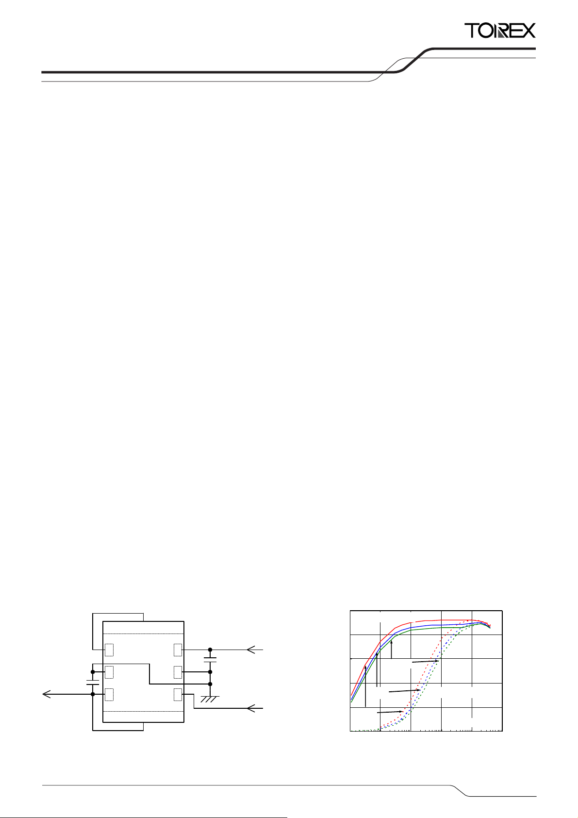
TYPICAL APPLICATION CIRCUIT
C
L
10μF
400mA
* “L1 and L
level as a result of this function.
SS
XCL201/XCL202 Series
L1
L
Vss
V
OUT
(TOP VIEW)
”, and “L2 and V
X
VIN
Vss
CE
L2
” is connected by wiring.
OUT
C
IN
4.7μF
■FEATURES
Ultra Small : 2.5mm×2.0mm, h=1.0mm
Input Voltage : 2.0V ~ 6.0V
Output Voltage : 0.8V ~ 4.0V (±2.0%)
High Efficiency : 92%(VIN=4.2V,V
Output Current : 400mA
Oscillation Frequency : 1.2MHz (±15%)
Maximum Duty Cycle : 100%
Output Capacitor : Low ESR Ceramic
Current Limiter Circuit : Constant Current & Latching
Control Methods : PWM (XCL201)
PWM/PFM Auto (XCL202)
CE Function : Soft-Start Circuit Built-In
Operating Ambient Temperature
Environmentally Friendly : EU RoHS Compliant, Pb Free
TYPICAL PERFORMANCE
CHARACTERISTICS
100
80
60
40
Efficency:EFFI(%
20
to be discharged via the internal
L
XCL201B331BR/XCL202B331BR
XCL202(PWM/PFM)
4.2V
0
0.01 0.1 1 10 100 1000
☆GreenOperation Compatible
: -40℃〜+85℃
VIN = 5.5V
5.0V
Output Curr ent:I
XCL201(PWM)
VOUT=3.3V
(mA)
OUT
auto
L
OUT
=3.3V)
1/21
XCL201/XCL202 Series
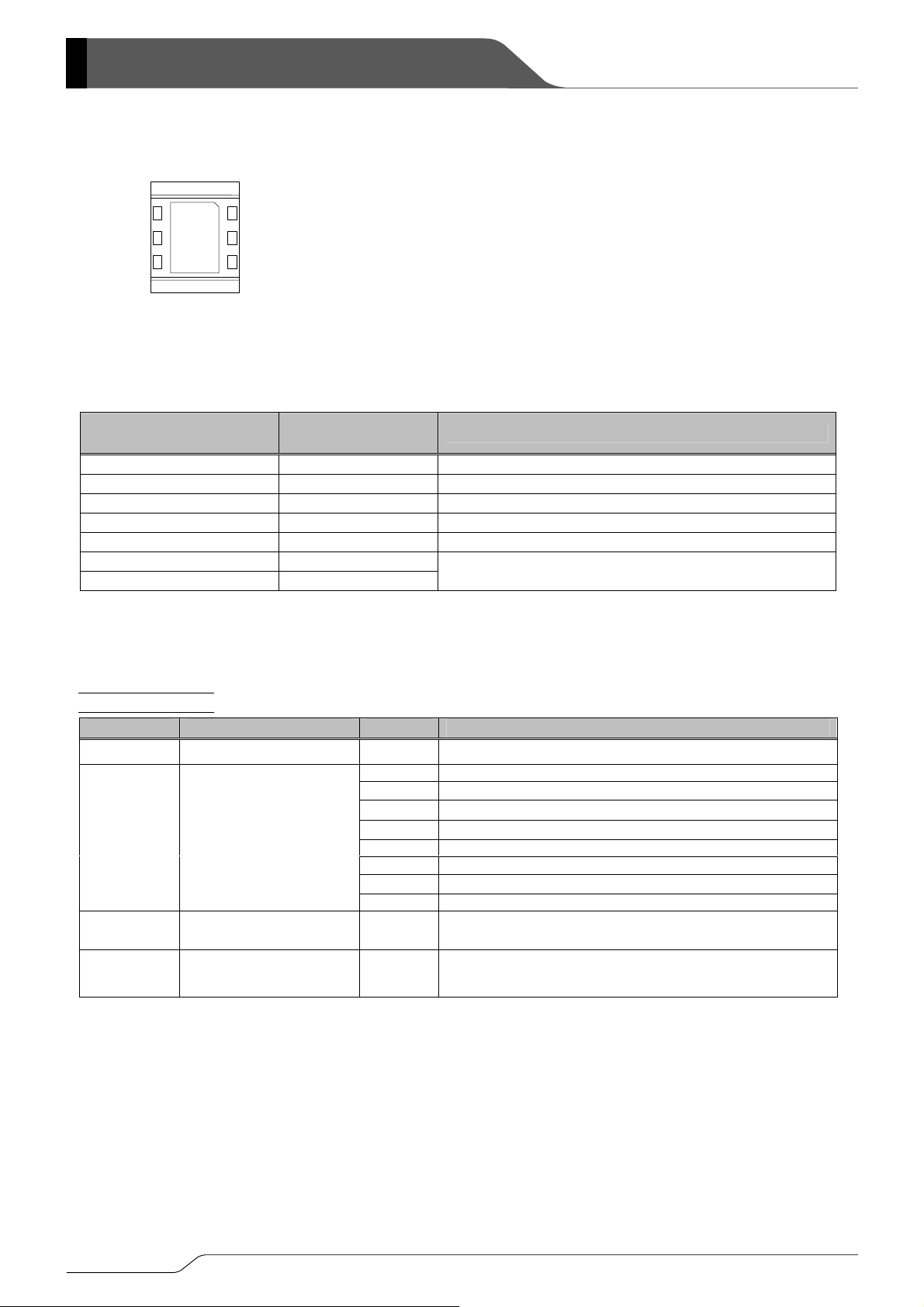
■PIN CONFIGURATION
L1
7
1
6
V
IN
5
Vss
CE
4
8
L2
(BOTTOM VIEW)
■PIN ASSIGNMENT
Lx
Vss
2
VOUT
3
* It should be connected the VSS pin (No. 2 and 5) to the GND pin.
* If the dissipation pad needs to be connected to other pins, it should be connected to the GND pin.
* Please refer to pattern layout page for the connecting to PCB.
PIN NUMBER PIN NAME
FUNCTION
1 Lx Switching Output
2,5 VSS Ground
3 V
Output Voltage
OUT
4 CE Chip Enable
6 VIN Power Input
7 L1
8 L2
Inductor Electrodes
■PRODUCT CLASSIFICATION
●Ordering Information
XCL201①②③④⑤⑥-⑦
XCL202①②③④⑤⑥-⑦
(*1)
Fixed PWM control
(*1)
PWM / PFM automatic switching control
DESIGNATOR ITEM SYMBOL DESCRIPTION
①
②③
Functions selection B C
Output Voltage
(*2)
auto discharge, High speed soft-start
L
10 1.0V
12 1.2V
15 1.5V
18 1.8V
25 2.5V
28 2.8V
30 3.0V
33 3.3V
④
⑤⑥-⑦
(*1)
The “-G” suffix denotes Halogen and Antimony free as well as being fully RoHS compliant.
(*2)
When other output voltages are needed, please contact your local Torex sales office for more information.
Output voltage range is 0.8~4.0V.
(*1)
Oscillation Frequency 1 1.2MHz
Package
(Order Unit)
BR-G CL-2025 (3,000/Reel)
2/21

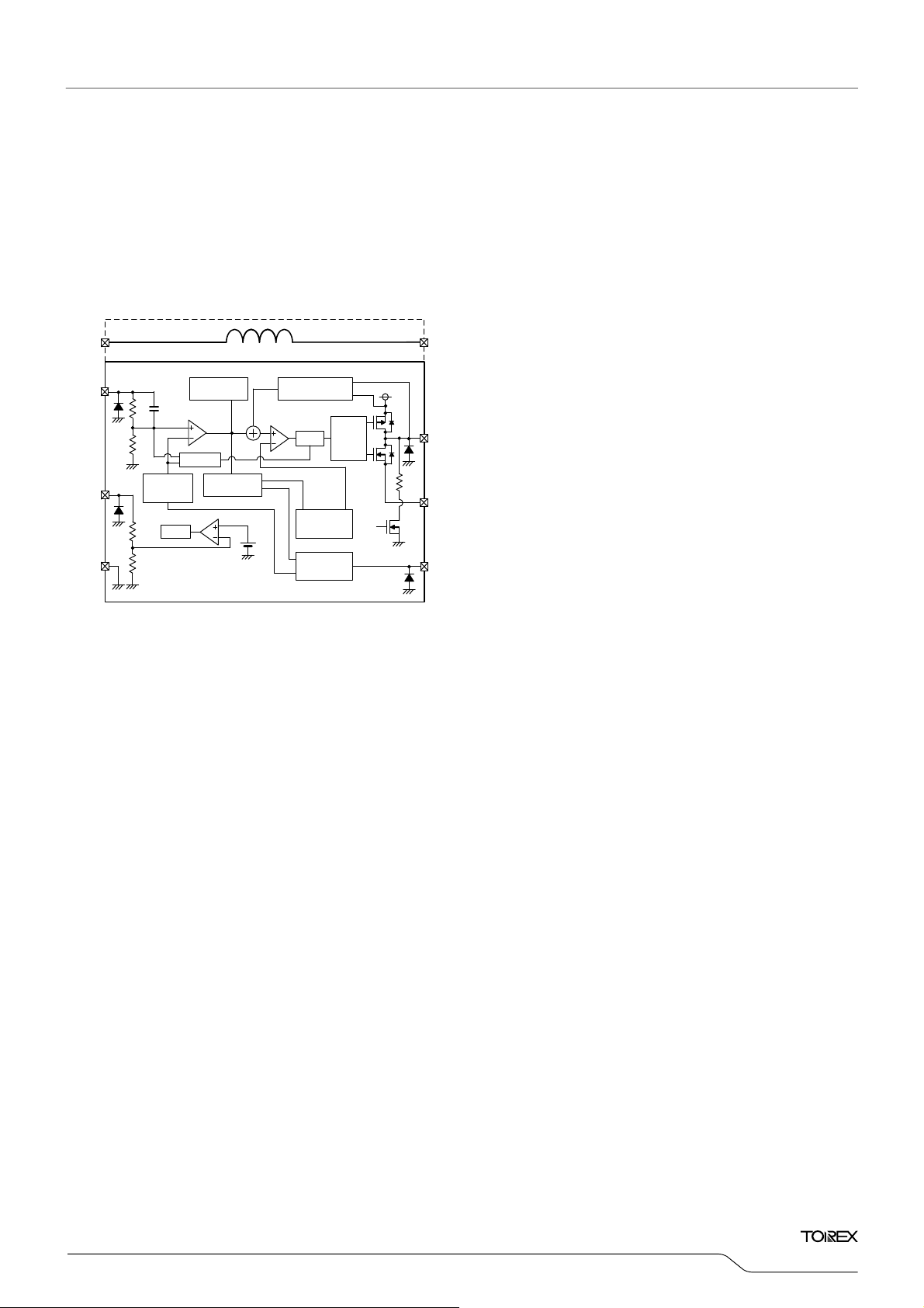
■BLOCK DIAGRAM
●XCL201B / XCL202B Series
XCL201/XCL202
Series
L2 L1
VOUT
CFB
R1
FB
V
R2
VIN
SS
R3
R4
Vref with
Soft Start,
CE
UVLO
VSHORT
Phase
Compensation
Error
Amp.
PWM/PFM
Selector
UVLO Cmp
Inductor
Current Feedback
PWM
Comparator
Current Limit
Logic
Ramp Wave
Generator
OSC
CE
Control
Logic
Synch
Buffer
Drive
Lx
VSS
CE/
CE
NOTE: The XCL201 offers a fixed PWM control, a signal from CE Control Logic to PWM/PFM Selector is fixed to "L" level inside. The
XCL202 control scheme is PWM/PFM automatic switching, a signal from CE Control Logic to PWM/PFM Selector is fixed to "H" level
inside. The diodes placed inside are ESD protection diodes and parasitic diodes.
■ABSOLUTE MAXIMUM RATINGS
Ta = 2 5 ℃
PAR AMET ER SYMBOL RATINGS UNITS
VIN Pin Voltage VIN - 0.3 ~ 6.5 V
LX Pin Voltage VLX - 0.3 ~ V
V
Pin Voltage V
OUT
- 0.3 ~ 6.5 V
OUT
CE Pin Voltage VCE - 0.3 ~ 6.5 V
LX Pin Current I
±1500 mA
LX
Power Dissipation Pd 1000 *1 mW
Operating Ambient Temperature Topr - 40~ +85 ℃
Storage Temperature Tstg - 40 ~ +105 ℃
*1: The power dissipation figure shown is PCB mounted (40mm×40mm, t=1.6mm, Glass Epoxy FR-4).
Please refer to page 12 for details.
+ 0.3≦6.5 V
IN
3/21
XCL201/XCL202 Series
■ELECTRICAL CHARACTERISTICS
XCL201B121BR/XCL202B121BR, V
OUT
=1.2V, f
=1.2MHz, Ta=25℃
OSC
PARAMETER SYMBOL CONDITIONS
Output Voltage V
Operating Voltage Range
Maximum Output Current
UVLO Voltage V
Supply Current (XCL201) - 22 50
Supply Current (XCL202)
Stand-by Current I
Oscillation Frequency
PFM Switching Current
PFM Duty Limit
(*11)
I
(*11)
DTY
OUT
V
I
OUTMAX
UVLO
I
DD
STB
f
OSC
PFM
LIMIT_PFM
IN
Maximum Duty Cycle MAXDTY VIN=VCE=5.0V, V
Minimum Duty Cycle MINDTY VIN=VCE=5.0V, V
Efficiency
Lx SW "H" ON Resistance 1
Lx SW "H" ON Resistance 2
Lx SW "L" ON Resistance 1
Lx SW "L" ON Resistance 2
Lx SW "H" Leakage Current
Current Limit
Output Voltage
Temperature Characteristics
CE "H" Voltage V
CE "L" Voltage V
CE "H" Current I
CE "L" Current I
Soft Start Time
Latch Time
Short Protection
Threshold Voltage
CL Discharge
Inductance Value
Allowed Inductor Current I
Test conditions: Unless otherwise stated, VIN=5.0V, V
NOTE:
(*1)
Including hysteresis operating voltage range.
(*2)
EFFI= { ( output voltage×output current ) / ( input voltage×input current) }×100
(*3)
ON resistance (Ω)=(VIN - Lx pin measurement voltage) / 100mA
(*4)
Design value
(*5)
When temperature is high, a current of approximately 10μA (maximum) may leak.
(*6)
Time until it short-circuits V
(*7)
When VIN is less than 2.4V, limit current may not be reached because voltage falls caused by ON resistance.
(*8)
When the difference between the input and the output is small, some cycles may be skipped completely before current maximizes.
If current is further pulled from this state, output voltage will decrease because of P-ch driver ON resistance.
(*9)
Current limit denotes the level of detection at peak of coil current.
(*10)
“H”=VIN~VIN-1.2V, “L”=+0.1V~-0.1V
(*11)
I
and DTY
PFM
(*2)
EFFI
R
LxH1
R
LxH2
R
LxL1
R
(*5)
(*9)
I
LxL2
I
LeakH
LIM
△
V
OUT
(V
・△
OUT
CEH
CEL
CEH
CEL
t
SS
t
LAT
V
SHORT
R
DCHG
L Test frequency=1MHz - 4.7 - μH-
DC
with GND via 1Ω of resistor from an operational state and is set to Lx=0V from current limit pulse generating.
OUT
are defined only for the XCL202 series which have PFM control function. (Not for the XCL201 series)
LIMIT_PFM
When connected to external components,
V
IN=VCE
=5.0V, I
OUT
=30mA
2.0 - 6.0 V ①
V
IN=VOUT(T)
When connected to external components
V
CE=VIN,VOUT
Voltage which Lx pin holding “L” level
V
IN=VCE
VIN=5.0V, VCE=0V, V
When connected to external components,
V
IN=VOUT(T)
When connected to external components,
V
IN=VOUT(T)
VCE=VIN = 2.0V, I
+2.0V, VCE=1.0V
=0V
=5.0V, V
OUT=VOUT(T)
OUT
+2.0V, VCE=1.0V , I
+2.0V, VCE=VIN , I
=1mA - 200 300 % ①
OUT
OUT=VOUT (T)
OUT=VOUT (T)
When connected to external components,
V
CE=VIN=VOUT (T)
VIN=VCE=5.0V, V
VIN=VCE=3.6V, V
VIN=VCE=5.0V
VIN=VCE=3.6V
VIN=V
V
/
Topr)
OUT
IN=VCE
I
=30mA
OUT
-40℃≦Topr≦85℃
V
=0V, Applied voltage to VCE,
OUT
Voltage changes Lx to “H” level
V
=0V, Applied voltage to VCE,
OUT
Voltage changes Lx to “L” level
VIN=VCE=5.0V, V
V
=5.0V, VCE=0V, V
IN
When connected to external components,
=0V→V
V
CE
V
IN=VCE
Short Lx at 1Ω resistance
Sweeping V
1Ω resistance, V
level within 1ms
+1.2V, I
=0V,ILX=100mA
OUT
=0V,ILX=100mA
OUT
(*4)
- 0.45 0.66 Ω -
(*4)
- 0.52 0.77 Ω -
=5.0V, VCE=0V, LX=0V - 0.01 1.0 μA ⑨
=5.0V, V
=5.0V, V
OUT=VOUT (T)
=0V - 0.1 - 0.1 μA ⑤
OUT
OUT
, I
=1mA
IN
OUT
=0.8×V
OUT
, VIN=VCE=5.0V, Short Lx at
OUT
voltage which Lx becomes “L”
OUT
VIN=5.0V, LX=5.0V, VCE=0V, V
ΔT=40℃ - 600 - mA -
=Nominal Voltage
OUT(T)
(*8)
(*1, *10)
×1.1V
= V
×1.1V - 0 1.0 μA ③
OUT(T)
=100mA
OUT
=1mA
OUT
×0.9V 100 - - % ③
×1.1V - - 0 % ③
=100mA
OUT
×0.9V
(*10)
(*10)
(*3)
- 0.35 0.55 Ω ④
(*3)
- 0.42 0.67 Ω ④
(*7)
700 800 1000 mA ⑥
=0V - 0.1 - 0.1 μA ⑤
OUT(T)
(*6)
=open 200 300 450 Ω ⑧
OUT
MIN. TYP. MAX.
1.176 1.200 1.224 V ①
400 - - mA ①
1.00 1.40 1.78 V ②
- 15 33
1020 1200 1380 kHz ①
140 180 240 mA ⑩
- 86 - % ①
- ±100 - ppm/ ℃ ①
0.65 - 6.0 V ③
- 0.25 V ③
V
SS
- 0.25 0.40 ms ①
1.0 - 20 ms ⑦
0.450 0.600 0.750 V ⑦
UNITS
CIRCUIT
μA ②
4/21
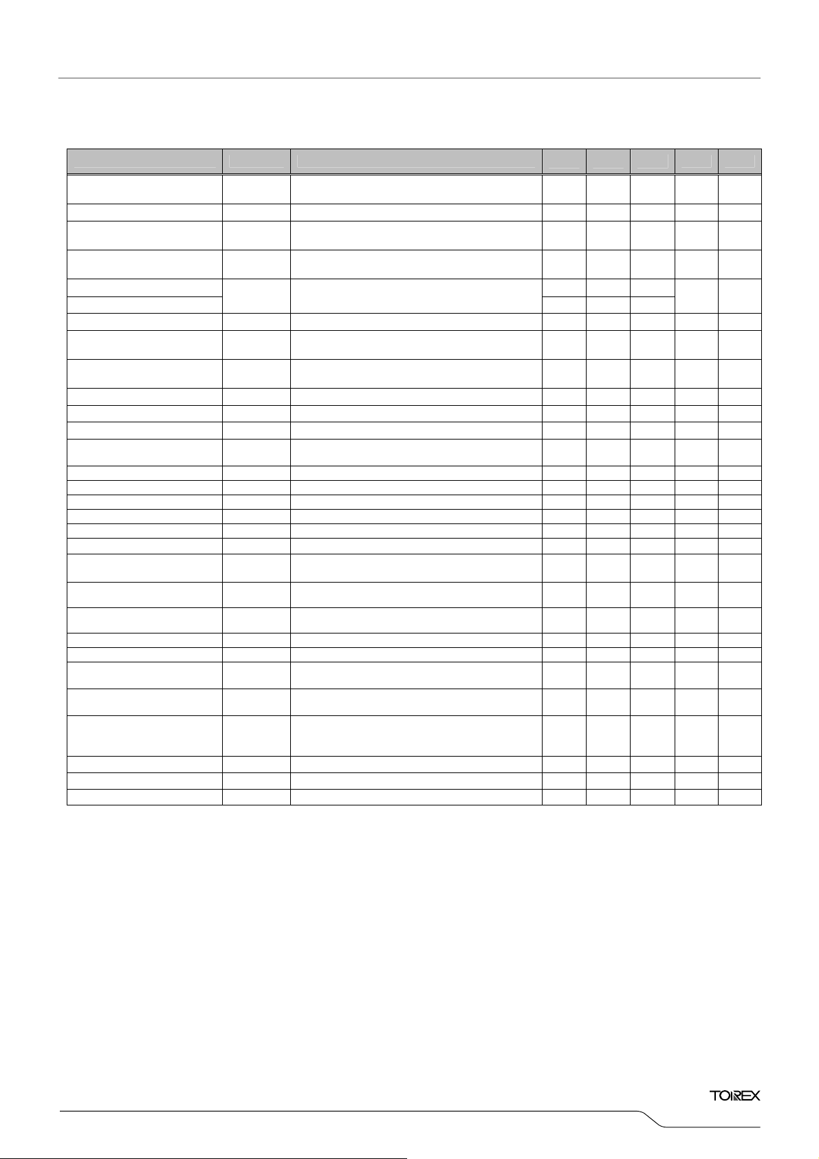
■ELECTRICAL CHARACTERISTICS (Continued)
XCL201B181BR/XCL202B181BR, V
OUT
=1.8V, f
=1.2MHz, Ta=25℃
OSC
XCL201/XCL202
Series
PARAMETER SYMBOL CONDITIONS
Output Voltage V
Operating Voltage Range
Maximum Output Current
UVLO Voltage V
Supply Current (XCL201) - 22 50
Supply Current (XCL202)
Stand-by Current I
Oscillation Frequency
PFM Switching Current
PFM Duty Limit
(*11)
(*11)
DTY
I
OUT
V
I
OUTMAX
UVLO
I
DD
STB
f
OSC
PFM
LIMIT_PFM
IN
Maximum Duty Cycle MAXDTY VIN=VCE=5.0V, V
Minimum Duty Cycle MINDTY VIN=VCE=5.0V, V
Efficiency
Lx SW "H" ON Resistance 1
Lx SW "H" ON Resistance 2
Lx SW "L" ON Resistance 1
Lx SW "L" ON Resistance 2
Lx SW "H" Leakage Current
Current Limit
Output Voltage
Temperature Characteristics
CE "H" Voltage V
CE "L" Voltage V
CE "H" Current I
CE "L" Current I
Soft Start Time
Latch Time
Short Protection
Threshold Voltage
CL Discharge
Inductance Value
Allowed Inductor Current I
Test conditions: Unless otherwise stated, VIN=5.0V, V
NOTE:
(*1)
Including hysteresis operating voltage range.
(*2)
EFFI={ ( output voltage×output current ) / ( input voltage×input current) }×100
(*3)
ON resistance (Ω)=(VIN - Lx pin measurement voltage) / 100mA
(*4)
Design value
(*5)
When temperature is high, a current of approximately 10μA (maximum) may leak.
(*6)
Time until it short-circuits V
(*7)
When VIN is less than 2.4V, limit current may not be reached because voltage falls caused by ON resistance.
(*8)
When the difference between the input and the output is small, some cycles may be skipped completely before current maximizes.
If current is further pulled from this state, output voltage will decrease because of P-ch driver ON resistance.
(*9)
Current limit denotes the level of detection at peak of coil current.
(*10)
“H”=VIN~VIN-1.2V, “L”=+0.1V~-0.1V
(*11)
I
and DTY
PFM
(*2)
EFFI
R
LxH1
R
LxH2
R
LxL1
R
(*5)
(*9)
I
LxL2
I
LeakH
LIM
△
V
OUT
(V
・△
OUT
CEH
CEL
CEH
CEL
t
SS
t
LAT
V
SHORT
R
DCHG
L Test frequency=1MHz - 4.7 - μH-
DC
with GND via 1Ω of resistor from an operational state and is set to Lx=0V from current limit pulse generating.
OUT
are defined only for the XCL202 series which have PFM control function. (Not for the XCL201 series)
LIMIT_PFM
When connected to external components,
V
IN=VCE
=5.0V, I
OUT
=30mA
2.0 - 6.0 V ①
V
IN=VOUT(E)
When connected to external components
V
CE=VIN,VOUT
Voltage which Lx pin holding “L” level
V
IN=VCE
VIN=5.0V, VCE=0V, V
When connected to external components,
V
IN=VOUT(T)
When connected to external components,
V
IN=VOUT(T)
VCE=VIN=V
+2.0V, VCE=1.0V
=0V
=5.0V, V
OUT=VOUT(T)
OUT=VOUT(T)
+2.0V, VCE=1.0V , I
+2.0V, VCE=VIN , I
+0.5V, I
OUT(T)
OUT=VOUT (T)
OUT=VOUT (T)
(*8)
(*1, *10)
×1.1V
×1.1V - 0 1.0 μA ③
=100mA
OUT
=1mA
OUT
=1mA - 200 300 % ①
OUT
×0.9V 100 - - % ③
×1.1V - - 0 % ③
When connected to external components,
V
CE=VIN=VOUT (T)
VIN=VCE=5.0V, V
VIN=VCE=3.6V, V
VIN=VCE=5.0V
VIN=VCE=3.6V
VIN=V
V
/
Topr)
V
OUT
IN=VCE
=30mA
I
OUT
-40℃≦Topr≦85℃
V
=0V, Applied voltage to VCE,
OUT
Voltage changes Lx to “H” level
V
=0V, Applied voltage to VCE,
OUT
Voltage changes Lx to “L” level
IN=VCE
VIN=5.0V, VCE=0V, V
When connected to external components,
V
=0V→V
CE
V
IN=VCE
Short Lx at 1Ω resistance
Sweeping V
1Ω resistance, V
“L” level within 1ms
VIN=5.0V LX=5.0V VCE=0V V
+1.2V, I
OUT
OUT
(*4)
- 0.45 0.66 Ω -
(*4)
- 0.52 0.77 Ω -
=5.0V, VCE=0V, L
= 5.0V, V
=5.0V, V
=5.0V, V
OUT=VOUT (T)
OUT
, I
IN
OUT
OUT
, VIN=VCE=5.0V, Short Lx at
OUT
OUT
=100mA
OUT
=0V, ILX=100mA
=0V, ILX=100mA
X
=0V - 0.1 - 0.1 μA ⑤
=0V - 0.1 - 0.1 μA ⑤
OUT
=1mA
=0.8×V
(*6)
voltage which Lx becomes
(*3)
- 0.35 0.55 Ω ④
(*3)
- 0.42 0.67 Ω ④
=0V - 0.01 1.0 μA ⑨
(*7)
×0.9V
OUT(T)
700 800 1000 mA ⑥
(*10)
(*10)
=open 200 300 450 Ω ⑧
OUT
ΔT=40℃ - 600 - mA -
=Nominal Voltage
OUT (T)
MIN. TYP. MAX.
1.764 1.800 1.836 V ①
400 - - mA ①
1.00 1.40 1.78 V ②
- 15 33
1020 1200 1380
120 160 200 mA ⑩
- 89 - % ①
- ±100 - ppm/ ℃ ①
0.65 - 6.0 V ③
- 0.25 V ③
V
SS
- 0.32 0.50 ms ①
1.0 - 20 ms ⑦
0.675 0.900 1.125 V ⑦
UNITS
CIRCUIT
μA ②
kHz ①
5/21

XCL201/XCL202 Series
■ELECTRICAL CHARACTERISTICS (Continued)
The value and conditions are depends on setting output voltage.
●PFM Switching Current (I
) (XCL202)
PFM
NOMINAL OUTPUT VOLTAGE MIN. TYP. MAX.
0.8V≦V
1.2V<V
1.8V≦V
OUT(T)
OUT(T)
OUT(T)
≦1.2V
<1.8V
≦4.0V
140mA 180mA 240mA
130mA 170mA 220mA
120mA 160mA 200mA
●PFM Duty Limit DTY
LIMIT_PFM
(XCL202)
SETTING VOLTAGE CONDITIONS
0.8V≦V
1.0V≦V
<1.0V
OUT(T)
≦4.0V V
OUT(T)
=2.0V, I
V
CE=VIN
CE=VIN=VOUT(T)
=1mA
OUT
+0.5V, I
OUT
●Soft-Start Time t
SERIES OUTPUT VOLTAGE MIN. TYP. MAX.
SS
=1mA
- 0.25ms 0.40ms
- 0.32ms 0.50ms
- 0.28ms 0.40ms
- 0.32ms 0.50ms
- 0.28ms 0.40ms
- 0.32ms 0.50ms
XCL201B
XCL202B
0.8V≦V
1.5V≦V
1.8V≦V
2.5V≦V
0.8V≦V
2.5V≦V
OUT(T)
OUT(T)
OUT(T)
OUT(T)
OUT(T)
OUT(T)
<1.5V
<1.8V
<2.5V
≦4.0V
<2.5V
≦4.0V
■TYPICAL APPLICATION CIRCUIT
XCL201/XCL202 Series
L1
Lx
Vss
C
L
OUT
V
●External Components
C
: 10V/4.7μF(Ceramic)
IN
C
: 6.3V/10μF(Ceramic)
L
NOTE:
The Inductor can be used only for this DC/DC converter.
Please do not use this inductor for the other reasons.
Please use B, X5R, and X7R grades in temperature characteristics for C
These grade ceramic capacitors minimize capacitance-loss as a function of voltage stress.
L2
V
IN
Vss
CE
C
IN
and CL capacitors.
IN
6/21
XCL201/XCL202
Series
■OPERATIONAL DESCRIPTION
The XCL201/XCL202 series consists of a reference voltage source, ramp wave circuit, error amplifier, PWM comparator, phase compensation
circuit, output voltage adjustment resistors, P-channel MOSFET driver transistor, N-channel MOSFET switching transistor for the synchronous
switch, current limiter circuit, UVLO circuit with control IC, and an inductor. (See the block diagram below.) Using the error amplifier, the voltage
of the internal voltage reference source is compared with the feedback voltage from the V
compensation is performed on the resulting error amplifier output, to input a signal to the PWM comparator to determine the turn-on time during
PWM operation. The PWM comparator compares, in terms of voltage level, the signal from the error amplifier with the ramp wave from the ramp
wave circuit, and delivers the resulting output to the buffer driver circuit to cause the Lx pin to output a switching duty cycle. This process is
continuously performed to ensure stable output voltage. The current feedback circuit monitors the P-channel MOS driver transistor current for
each switching operation, and modulates the error amplifier output signal to provide multiple feedback signals. This enables a stable feedback
loop even when a low ESR capacitor such as a ceramic capacitor is used ensuring stable output voltage.
L2 L1
Inductor
VOUT
V
VIN
CFB
R1
FB
R2
Vref with
Soft Start,
R3
SS
R4
CE
UVLO
Phase
Compensation
Error
Amp.
VSHORT
UVLO Cmp
PWM/PFM
Selector
Current Feedback
PWM
Comparator
Current Limit
Logic
Ramp Wave
Generator
OSC
CE
Control
Logic
Synch
Buffer
Drive
Lx
VSS
CE/
CE
<Reference Voltage Source>
The reference voltage source provides the reference voltage to ensure stable output voltage of the DC/DC converter.
<Ramp Wave Circuit>
The ramp wave circuit determines switching frequency. The frequency is fixed internally 1.2MHz. Clock pulses generated in this circuit are
used to produce ramp waveforms needed for PWM operation, and to synchronize all the internal circuits.
<Error Amplifier>
The error amplifier is designed to monitor output voltage. The amplifier compares the reference voltage with the feedback voltage divided by the
internal split resistors, R1 and R2. When a feed back voltage is lower than the reference voltage, the output voltage of the error amplifier is
increased. The gain and frequency characteristics of the error amplifier output are fixed internally to deliver an optimized signal to the mixer.
pin through split resistors, R1 and R2. Phase
OUT
7/21
 Loading...