

Torex XCL102, XCL103 Series Series Manual
XCL102/XCL103
Series
Inductor Built-in Step-up “micro DC/DC ” Converter (micro DC/DC)
■GENERAL DESCRIPTION
■APPLICATIONS
■FEATURES
Input Voltage Range
: 0.9V~6.0V (Absolute Max. Rating: 7.0V)
Fixed Output Voltage
: 2.2V~5.5V (0.1V increments)
Oscillation Frequency
: 3.0MHz (±20%)
Input Current
: 0.8A
Output Current
: 500mA @V
=5.0V, V
=3.3V (TYP.)
350mA @V
OUT
=3.3V, V
BAT
=1.8V (TYP.)
Control Mode Selection
Load Transient Response
: PWM (XCL102 Series) or
:
→200mA
Protection Circuits
: Over-current limit (Integral latch method)
Output short-circuit protection
Functions
: Soft-start
Load Disconnection Function (D type)
CL Auto Discharge Function (D type)
Bypass Switch Function (E type)
Output Capacitor
: Ceramic Capacitor
Operating Ambient T emperature
: -40℃~+85℃
Package
: CL-2025-02
Environmentally Friendly
: EU RoHS Compliant, Pb Free
■
GreenOperation-Compatible
CHARACTERISTICS
C
L
7
8
1
2
3
4
5
6
Lx
V
OUT
V
BAT
GND
CE
GND
V
OUT
V
BAT
V
CE
C
IN
L1
L2
The XCL102/XCL103 series is a synchronous step-up micro DC/DC converter which integrates an inductor and a control IC
in one t iny package (2.0m m×2.5mm, h=1.0mm). A stable step-up pow er supply is configure d using only two capa citors connected
externally. An inter nal coi l sim plifies the circuit and enables minimization of noise and other operat iona l t rou ble due to the circuit
wiring. A wide operating voltage range of 0.9V to 6.0V enables support for applications that require an internally fixed output
voltage (2.2V to 5.5V). PWM control (XCL102) or automatic PWM/PFM switching control (XC L103) can be selecte d.
During the devices enter stand-by mode, XCL102D/XCL103D types prevent the application malfunction by C
Function which can quickly discharge the electric charge at the output capacitor (CL). XCL102/XCL103E types is able t o drive
Real Time Clock etc.
●Portable equipment
●Beauty & health equipment
●Wearable devices
●Game & Hobby
●PC Peripherals
●Devices with 1~3 Alkaline,
1~3 Nickel Hydride, 1 Lithium and 1 Li-ion
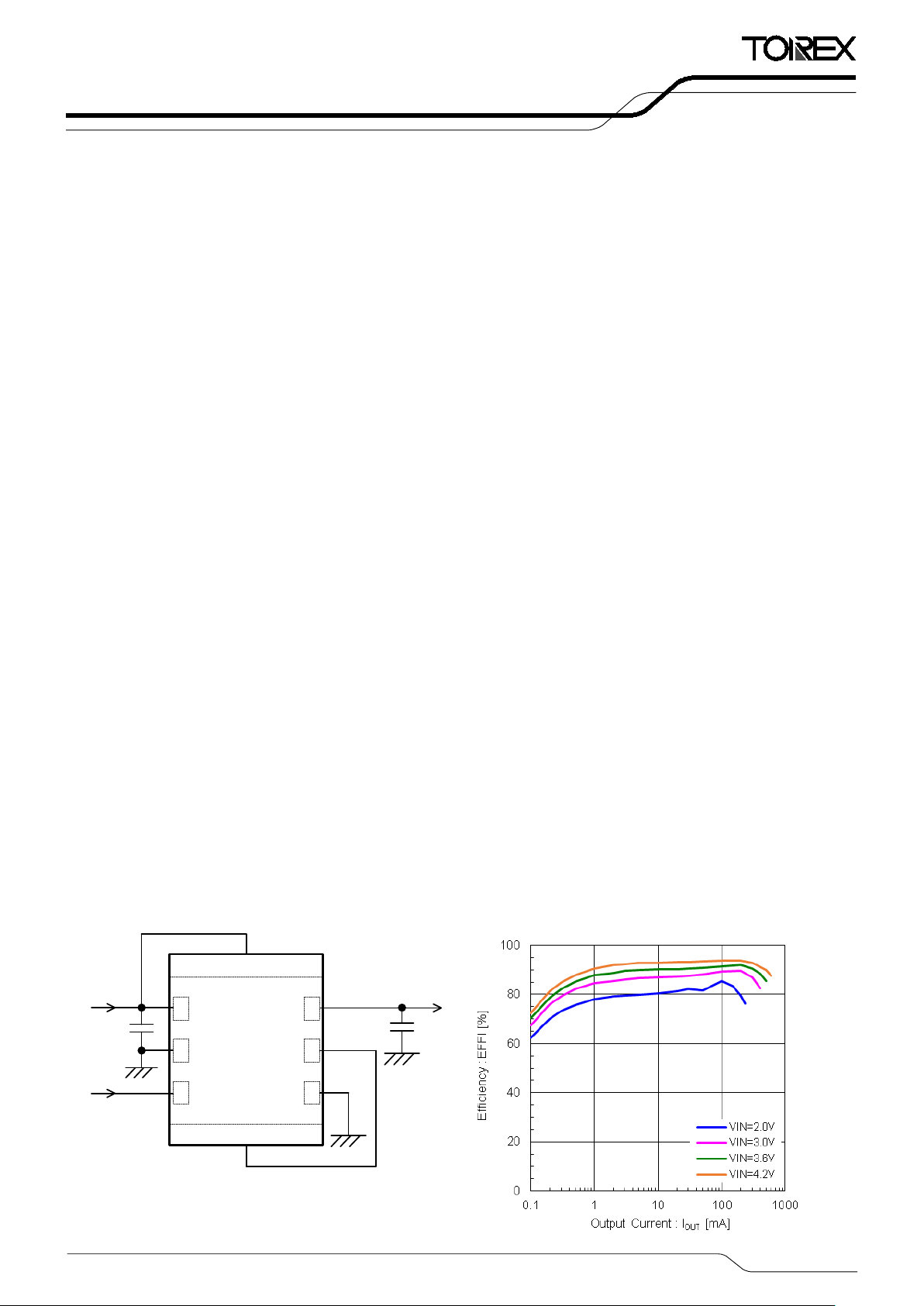
TYPICAL APPLICA TION CIRCUIT
■TYPICAL PERFORMANCE
Auto PWM/PFM (XCL103 Series)
100mV@V
XCL103D503CR-G/XCL103E503CR-G
☆
OUT
OUT
=3.3V,V
ETR28011-002
Discharge
L
BAT
BAT
=1.8V,I
OUT
=1mA
1/20
XCL102/XCL103 Series
VDD MAX
R
FB1
Load Disconn ect
Controller
CE Controlle r
Logic
PWM
Comparator
Buffer
Drive
L
X
V
BAT
V
OUT
Current sen se
Short-circuit
pro tection
Latch Ti m er
V re f with
Soft Start
C
FB
Inductor
GND
L2
L1
PFM/PW M
Controller Lo gic
V
DD
CE
V
OUT
C
L
Discharg e
Error Amp.
Phase
Compensa tion
RAMP Wave
Generator
OSC
R
FB2
FB
V
OUT
VDD MAX
R
FB1
Load Disconn ect
Controller
CE Controlle r
Logic
PWM
Comparator
Buffer
Drive
L
X
V
BAT
V
OUT
Current sen se
Short-circuit
pro tection
Latch Ti m er
V re f with
Soft Start
C
FB
Inductor
GND
L2
L1
PFM/PWM
Controller Lo gic
V
DD
CE
V
OUT
Bypass SW
Error Amp.
Phase
Compensa tion
RAMP Wave
Generator
OSC
R
FB2
FB
V
OUT
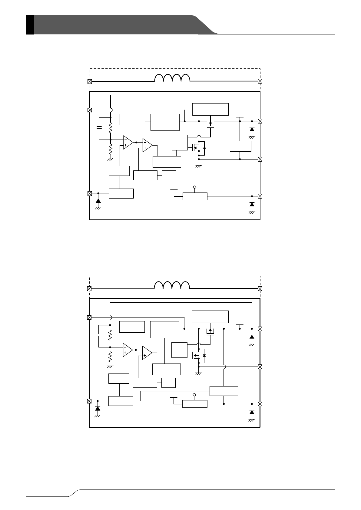
■ BLOCK DIAGRAM
2/20
●XCL102D/XCL103D series
* Diodes inside the circuits are ESD protection diodes and parasitic diodes.
* XCL102 series chooses only PWM control.
●XCL102E/XCL103E series
* Diodes inside the circuits are ESD protection diodes and parasitic diodes.
* XCL103 series chooses only PWM control.

XCL102/XCL103
D
E
Output Voltage options
5.0V → ②=5, ③=0
Oscillation Frequency
3
3.0MHz
Short
with latch
D
Fixed
Yes
Fixed
Yes
No
Yes
Yes
Yes
E
Fixed
Yes
Fixed
No
Yes
No
Yes
Yes
1
V
BAT
Power Input
2
GND
Ground
3
CE
Chip Enable
4
GND
Ground
5
Lx
Switching
6
V
Output Voltage
7
L1
8
L2
* If the pad needs to be connected to other pins, it should be connected to the GND.
(*1)
The ”-G” suffix indicates that the products are Halogen and Antimony free as well as being fully EU RoHS compliant.
7 L1
8 L2
V
OUT
6
Lx 5
GN D 4
1 V
BA T
2 GN D
3 CE
■PRODUCT CLASSIFICATION
●Ordering Information
XCL102①②③④⑤⑥-⑦ PWM control
XCL103①②③④⑤⑥-⑦ PWM/PFM automatic switching control
DESIGNATOR ITEM SYMBOL DESCRIPTION
Series
① Type
②③ Output Voltage 22~55
④
⑤⑥-⑦
●
Selecti on guides
TYPE
(*1)
Package (Order Unit) CR-G CL-2025-02 (3,000pcs/Reel)
Output
Voltage
Chip
Enable
Soft-Start
CL Auto-
Discharge
■PIN CONFIGURATION
■PIN ASSIGNMENT
PIN NUMBER PIN NAME FUNCTIONS
OUT
Inductor Electrodes
Refer to Selection Guide
e.g.)3.3V → ②=3, ③=3
Bypass
Switch
(BOTTOM VIEW)
Load
Disconnection
Current Limit
(with integral latch)
Protection
■FUNCTION CHART
PIN NAME SIGNAL STATUS
* Do not leave the CE pin open.
CE
L Stand-by
H Active
3/20

XCL102/XCL103 Series
V
Pin Voltage
V
-0.3~+7.0
V
CE Pin Voltage
VCE
-0.3~+7.0
V
*GND are standard voltage for all of the voltage.
■ABSOLUTE MAXIMUM RATINGS
PARAMETER SYMBOL RATINGS UNITS
V
Pin Voltage V
BAT
-0.3~+7.0 V
BAT
Lx Pin Voltage VLx -0.3~+7.0 V
OUT
Power Dissipation Pd 1000 (40mm x 40mm Standard board)
OUT
(*3)
mW
Operating Ambient Temperature Topr -40~+85 ℃
Storage Temperature Tstg -55~+125 ℃
(*3)
The power dissipation figure shown is PCB mounted and is for reference only.
The mounting condition is please refer to PACKAGING INFORMATION.
Ta=25℃
4/20
XCL102/XCL103
V
OUT=VOUT(T)
1.03→V
OUT(T)
0.97
Quiescent Current
Supply Current
IDD
V
= V
-0.2V
-
<E-5>
3.0
mA
Oscillation Frequency
f
OSC
V
BAT
= V
OUT(T)
0.5, I
OUT
=100mA
2.4
3.0
3.6
MHz
Minimum Duty Cycle
D
V
= V
+0.5V
- - 0
%
Efficiency
V
= V
0.6, RL is selected with
Efficiency
EFFI
V
= V
0.6, I
= 100mA
-
90
(*3)
- % ① Stand-by Current
I
STB
V
BAT=VLx
=6.0V,VCE=0V,
- 0 1.0
μA
Short Protection
CL Discharge Resistance
Bypass SW
Voltage changes Lx to be generated.
Voltage changes Lx to“H” level
Inductance
L
Test Freq.=1MHz
-
1.5 - μH
■ELECTRICAL CHARACTERISTICS
●XCL102/XCL103 Series
PARAMETER SYMBOL CONDITIONS MIN. TYP. MAX. UNITS CIRCUIT
Input Voltage VIN
Output Voltage V
Operation Start Voltage V
Operation Hold Voltage V
OUT
HLD
Voltage to start oscillation while
ST1
RL=1kΩ
RL=1kΩ
×
×
- - 6.0 V
<E-1> <E-2> <E-3> V
- - 0.90 V
- 0.65 - V
Series
Ta=25℃
①
⑤
①
①
(XCL103 only)
Maximum Duty Cycle D
PFM Switching Current
(XCL103 only)
(XCL103 only)
Lx SW "Pch" ON
Resistance
Lx SW "Nch" ON
Resistance
Lx SW”H” Leakage
Current
Current Limit I
Integral Latch Time tLAT
Latch Release Voltage V
Threshold Voltage
Soft-Start Time tSS
Iq V
OUT=VBAT
OUT=VBAT
= V
+0.5V - 26 40 μA
OUT(T)
OUT(T)
×
V
MAX
MIN
I
PFM
EFFI
R
V
LXP
R
LXN
I
V
LXLH
LIM
RL is selected with VOUT(T), Refer to Table 1 0.9 1.2 1.5 V
LAT_R
V
SHORT
=1.2V, V
BAT
OUT=VBAT
V
=1.5V, RL is selected with V
BAT
OUT
OUT(T)
= V
-0.2V 88 93 98 %
OUT(T)
,
OUT(T)
Refer to Table 1
BAT
V
OUT(T)
BAT
BAT=VLx
×
OUT(T)
, Refer to Table 1
×
OUT(T)
= 6.0V, I
OUT
=200mA - 0.3
OUT
(*1)
=6.0,VCE=0V, VLx=6.0V,V
BAT
= V
V
BAT
V
BAT
-0.2V, RLx=1Ω
OUT(T)
= V
-0.2V, RLx=1Ω, Time from
OUT(T)
=0V - 0 1.0 μA
OUT
current limit start to stop Lx oscillation
= V
OUT(T)
-0.2V, RL=1Ω
×0.6, V
OUT=VOUT(T)
× 0.9,
V
BAT=VOUT(T)
V
BAT
After "H" is fed to CE, the time by when
- 165 230 mA
- 86
- 0.3
(*3)
- %
(*2)
- Ω
(*3)
- Ω
<E-6> <E-7> <E-8> A
25 100 365 μs
-
(*3)
- V
0.2 0.5 1.0 ms
clocks are generated at Lx pin.
③
③
①
⑤
⑤
①
①
⑦
④
①
⑦
⑥
⑥
①
①
⑤
(Type D only)
Resistance (Type E only)
CE "H" Voltage V
CE "L" Voltage V
CE "H" Current I
CE "L" Current I
Inductor Rated Current I
V
:Target Voltage
OUT(T)
Test Conditions: unless otherwise stated、V
(*1)
XCL102D/XCL103D: V
(*2)
Design value for the XCL103D
(*3)
Designed value
R
V
DCHG
R
BSW
CEH
CEL
CEH
CEL
CEL
=0V, XCL102E/XCL103E: V
OUT
BAT
V
BAT
V
OUT
V
OUT
V
BAT
V
BAT
ΔT=+40deg - 1000 - mA
=1.5V, VCE=3.3V, Lx:OPEN, RLx=56Ω
BAT
=3.3V, V
= 3.3V, V
= V
= V
=6.0V,V
=6.0V,V
=3.3V, VCE=0V 100 180 400 Ω
OUT
=0V, VCE=0V 100 180 400 Ω
OUT
-0.15V, Applied voltage to VCE,
OUT(T)
-0.15V, Applied voltage to VCE,
OUT(T)
=6.0V, VLx=6.0V VCE=6.0V, -0.1 - 0.1 μA
OUT
=6.0V, VLx=6.0V ,VCE=0V -0.1 - 0.1 μA
OUT
=OPEN
OUT
0.8 - 6.0 V
GND - 0.2 V
②
②
⑤
⑤
②
②
-
-
5/20
XCL102/XCL103 Series
UNITS
V V V
mA A A
A
V
OUT(T)
MIN.
TYP.
MAX.
TYP.
MIN.
TYP.
MAX.
2.2
2.156
2.200
2.244
0.705
-
1.11
2.30
2.3
2.254
2.300
2.346
0.736
-
1.14
2.30
2.4
2.352
2.400
2.448
0.767
-
1.17
2.30
2.5
2.450
2.500
2.550
0.797
-
1.19
2.30
3.8
3.724
3.800
3.876
1.195
1.00
1.30
2.30
3.9
3.822
3.900
3.978
1.225
1.01
1.30
2.30
4.0
3.920
4.000
4.080
1.256
1.01
1.30
2.30
4.1
4.018
4.100
4.182
1.286
1.02
1.30
2.30
4.2
4.116
4.200
4.284
1.317
1.02
1.30
2.30
4.3
4.214
4.300
4.386
1.348
1.03
1.30
2.30
4.4
4.312
4.400
4.488
1.378
1.03
1.30
2.30
4.5
4.410
4.500
4.590
1.409
1.04
1.30
2.30
5.5
5.390
5.500
5.610
1.715
1.09
1.30
2.30
■ELECTRICAL CHARACTERISTICS (Continued)
Table 1. Extern al Components RL Table
V
RL
OUT(T)
UNITS:V
2.2≦V
3.1≦V
4.3≦V
OUT(T)
OUT(T)
OUT(T)
<3.1
<4.3
≦5.5
UNITS:Ω
220
330
470
Table 2. SPEC Table
NOMINAL
OUTPUT
VOLTAGE
<E-1> <E-2> <E-3> <E-5> <E-6> <E-7> <E-8>
V
OUT
IDD I
LIM
2.6 2.548 2.600 2.652 0.828 - 1.22 2.30
2.7 2.646 2.700 2.754 0.858 - 1.24 2.30
2.8 2.744 2.800 2.856 0.889 - 1.26 2.30
2.9 2.842 2.900 2.958 0.919 - 1.28 2.30
3.0 2.940 3.000 3.060 0.950 0.96 1.30 2.30
3.1 3.038 3.100 3.162 0.981 0.97 1.30 2.30
3.2 3.136 3.200 3.264 1.011 0.97 1.30 2.30
3.3 3.234 3.300 3.366 1.042 0.98 1.30 2.30
3.4 3.332 3.400 3.468 1.072 0.98 1.30 2.30
3.5 3.430 3.500 3.570 1.103 0.99 1.30 2.30
3.6 3.528 3.600 3.672 1.134 0.99 1.30 2.30
3.7 3.626 3.700 3.774 1.164 1.00 1.30 2.30
4.6 4.508 4.600 4.692 1.439 1.04 1.30 2.30
4.7 4.606 4.700 4.794 1.470 1.05 1.30 2.30
4.8 4.704 4.800 4.896 1.501 1.06 1.30 2.30
4.9 4.802 4.900 4.998 1.531 1.06 1.30 2.30
5.0 4.900 5.000 5.100 1.562 1.07 1.30 2.30
5.1 4.998 5.100 5.202 1.592 1.07 1.30 2.30
5.2 5.096 5.200 5.304 1.623 1.08 1.30 2.30
5.3 5.194 5.300 5.406 1.653 1.08 1.30 2.30
5.4 5.292 5.400 5.508 1.684 1.09 1.30 2.30
6/20
 Loading...