■
■
A
■
■
XC9801/XC9802 Series
ETR0802_003a
Regulated Voltage Step-Up Charge Pump ICs
GENERAL DESCRIPTION
The XC9801 series are fixed regulated voltage step-up charge pump ICs which provide stable, highly efficient, positive
voltages with the only external components required being 2 capacitors.
Since regulating is done via the control of the charge pump's gate voltage waveform, ripple is minimal. Output voltage is
selectable in 100mV steps within a 2.5V ~ 6.0V range.
Control of the XC9802 switches to PFM (pulse skip) during light loads without affecting output impedance or ripple so that the
IC is protected against drops in efficiency. Connecting the SENSE pin to the GND pin allows the IC to be used as a voltage
doubler.
As well as the ultra small MSOP-8A and USP-8 packages, the small consumption current and high efficiencies of the series
make the XC9801 suitable for use with all types of battery operated applications.
PPLICATIONS
●Palm top computers, PDAs
●On board local power supplies
●Various battery powered devices
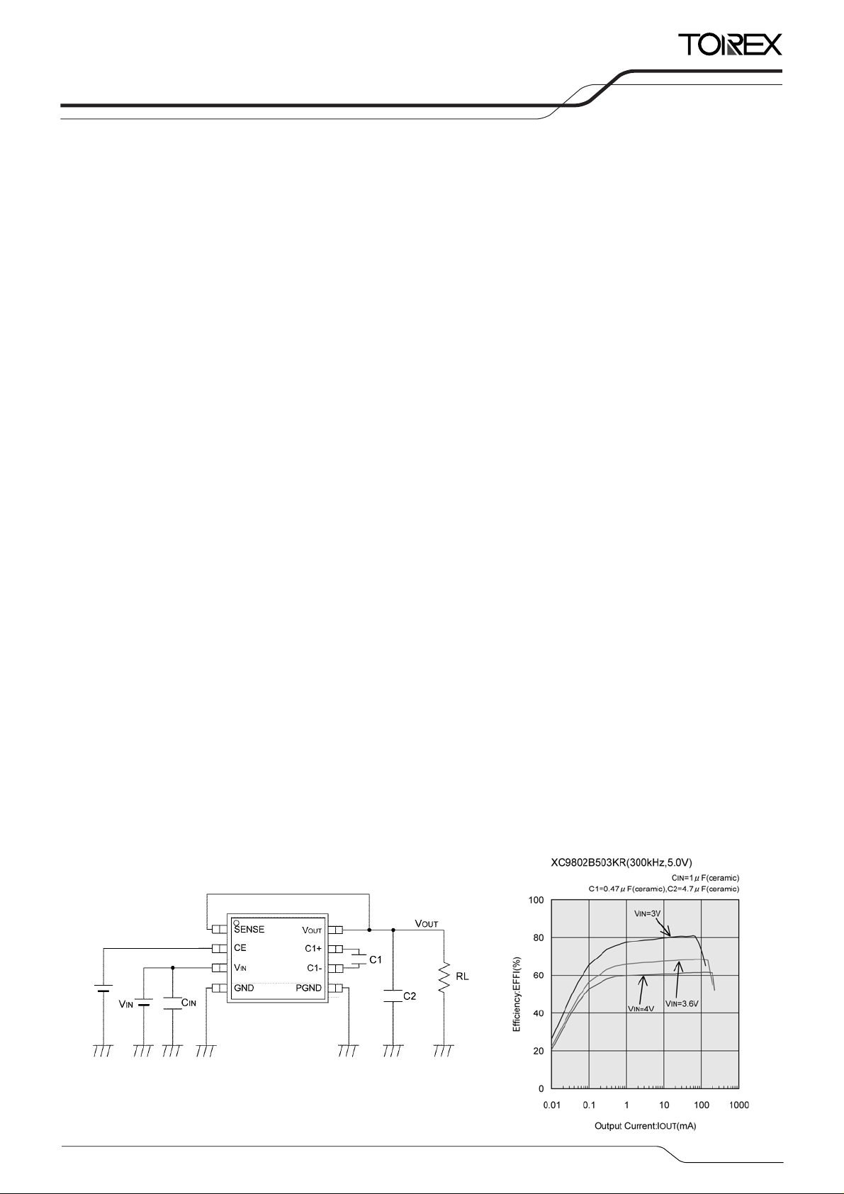
TYPICAL APPLICATION CIRCUIT
Regulation Output
FEATURES
Input Voltage Range : 1.8V ~ 5.5V
Output Voltage Range : 2.5V ~ 6.0V
Small Input Current : 80μA (no load:XC9802)
Output Current :
Oscillation Frequency : 300kHz
Stand-by Current (CE ’L’) : 2.0μA (MAX.)
PFM Operation During Light Loads (XC9802)
CE (Chip Enable) Function
Can be used as a step-up doubler (sense = 0V)
Packages : MSOP-8A, USP-8
Environmentally Friendly : EU RoHS Compliant, Pb Free
80mA (3.6V→5.0V step-up)
■TYPICAL PERFORMANCE
CHARACTERISTICS
1/12

■
■
■
(
XC9801/XC9802 Series
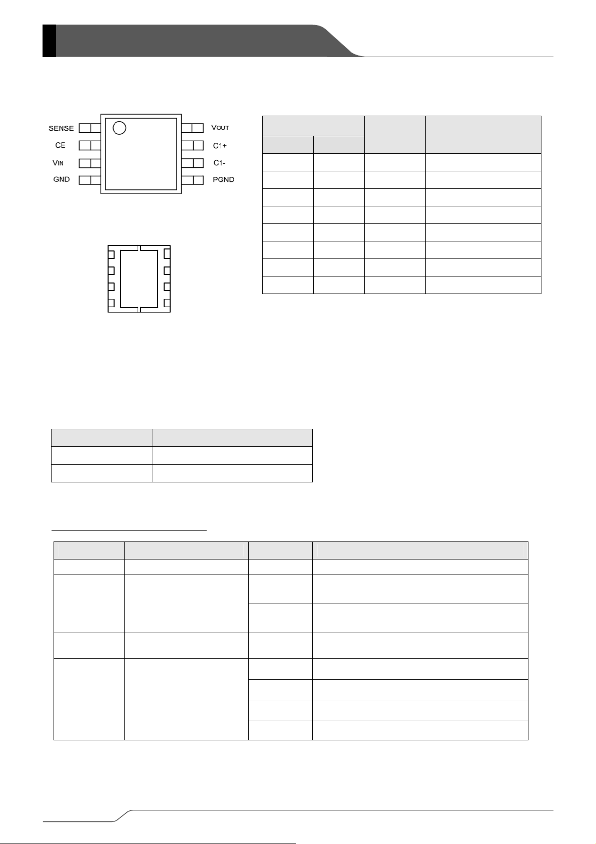
PIN CONFIGURATION
●Selection Guide
●Ordering Information
XC9801/XC9802 ①②③④⑤⑥‑⑦
1
2
3
4
PGND 5
VOUT 8
C1- 6
C1+ 7
C1+ 7
C1- 6
V
OUT 8
PGND 5
MSOP - 8A
(TOP VIEW)
1 SENSE
2 CE
3 V
4 GND
8
7
6
5
IN
USP-8
BOTTOM VIEW)
PRODUCT CLASSIFICATION
SERIES PULSE SKIP MODE
XC9801 Not Available
XC9802 Available
(*1)
PIN ASSIGNMENT
PIN NUMBER
USP-8 MSOP-8A
1 1 SENSE Output Voltage Monitor
2 2 CE Chip Enable (High Active)
3 3 VIN Input (Power Supply)
4 4 GND Ground
5 5 PGND Power Ground
6 6
7 7
8 8 VOUT Output
PIN NAME FUNCTION
C1−
C1+
External Capacitor - Pin
External Capacitor + Pin
DESIGNATOR
①
②③
④
True Logic Level at CE Pin B Positive
Oscillation Frequency 3 300kHz
ITEM SYMBOL DESCRIPTION
50
Output Voltage
25 ~ 60
Standard voltage
VOUT=5.0V→②=5, ③=0
Semi-custom voltage
OUT=2.5V→②=2, ③=5
e.g. V
KR MSOP-8A (1,000/Reel)
KR-G MSOP-8A (1,000/Reel)
⑤⑥-⑦
Packages (Order Unit)
DR USP-8 (3,000/Reel)
DR-G USP-8 (3,000/Reel)
Regulated output voltage function cannot be used by the following input voltage condition:
V
IN < (VOUT/2), or VIN ≧ VOUT
(*1)
The “-G” suffix indicates that the products are Halogen and Antimony free as well as being fully RoHS compliant.
2/12

■
■
A
XC9801/XC9802
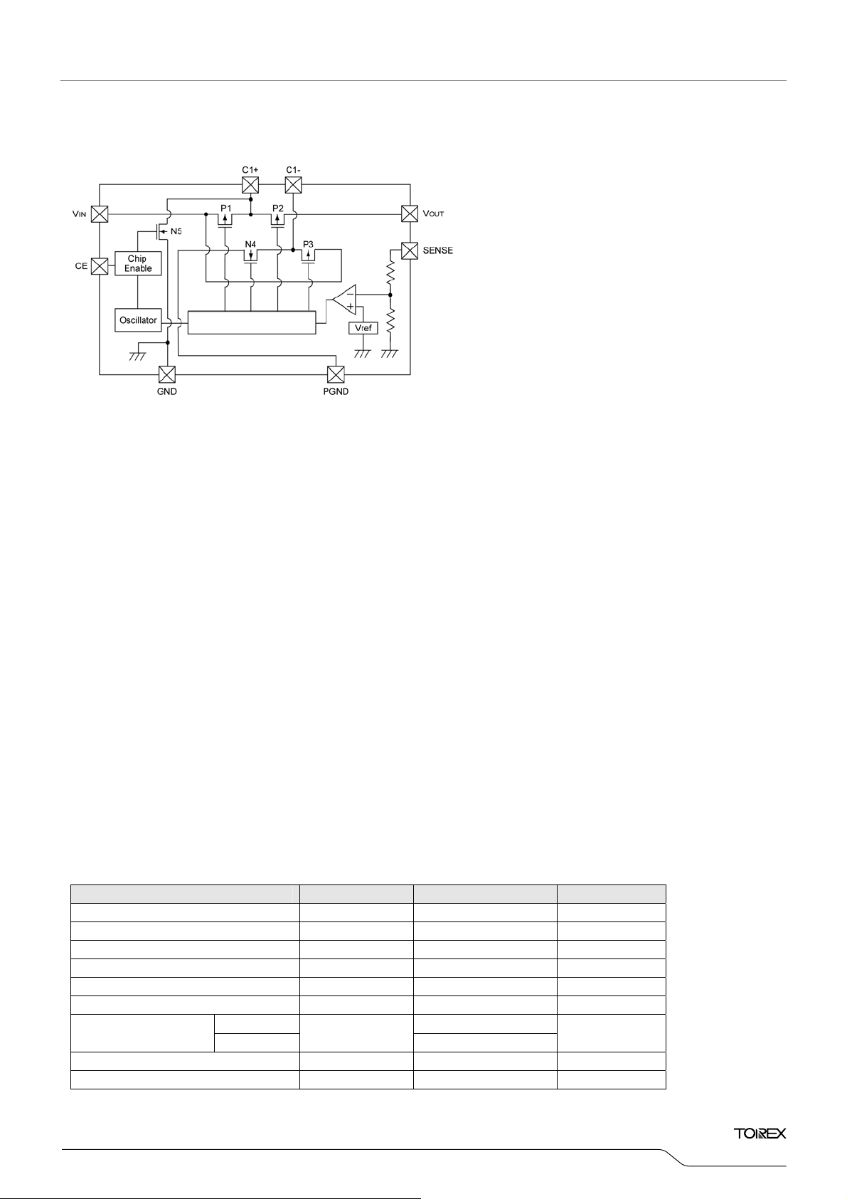
BLOCK DIAGRAM
(1) Basic Operations
Using the XC9801/02s clock generated by the internal oscillator, a step-up charge pump operation can be brought
about as a result of the alternate switching between operating conditions where P1 & N4 are ON with P2 & P3 OFF
(or) P1 & N4 are OFF with P2 & P3 ON. By connecting the SENSE pin to VOUT, output voltage can be f eedback and
the difference between the feedback voltage and the reference voltage (Vref) are compared by the internal operational
amplifier. Output voltage can be stabilized (* 2) by controlling P3s gate voltage waveform via the signal generated by
the internal amplifier.
Please note that this stabilizing function will not operate with V
By connecting SENSE to ground, the output stability function, as described above, can be halte d and the IC can be
used as a step-up doubler.
* 2 : As a result of P3 gradually reaching an ON state with each clock (signal), rush current is controlled, the ripple
decreases and with the combination of the independent phase compensation circuit, output voltage is stabilized
(2) Stand-by Function
When the voltage at CE (chip enable) is ‘low’ (0V), P1, P2 & P3 will be OFF with N4 & N5 ON. The external capacitor
C1 will discharge and impedance at V
(3) PFM (Pulse Skip) Operations
Whilst maintaining output voltage, the XC9802 provides the added security of protection agai nst drops in efficiency
during light loads as a result of the pulse, generated by the internal oscillator, being skipped and the operating
frequency being changed.
BSOLUTE MAXIMUM RATINGS
PARAMETER SYMBOL CONDITIONS UNITS
VIN pin Voltage VIN
VOUT pin Voltage VOUT
C1 + pin Voltage C1+
C1 - pin Voltage C1-
CE pin Voltage VCE
VOUT Pin Output Current IOUT 200 mA
Power Dissipation
Operating Temperature Range Topr
Storage Temperature Range T stg
Controller
IN < (VOUT/2) or VIN ≧ VOUT.
OUT will be high.
Ta = 25℃, GND = 0V
−0.3〜6.0
−0.3〜12.0
−0.3〜V
−0.3〜V
−0.3〜V
MSOP-8A 150
USP-8
Pd
OUT+0.3
OUT+0.3
IN+0.3
120
V
V
V
V
V
mW
−40〜+85 ℃
−40〜+125 ℃
Series
3/12

■
XC9801/XC9802 Series
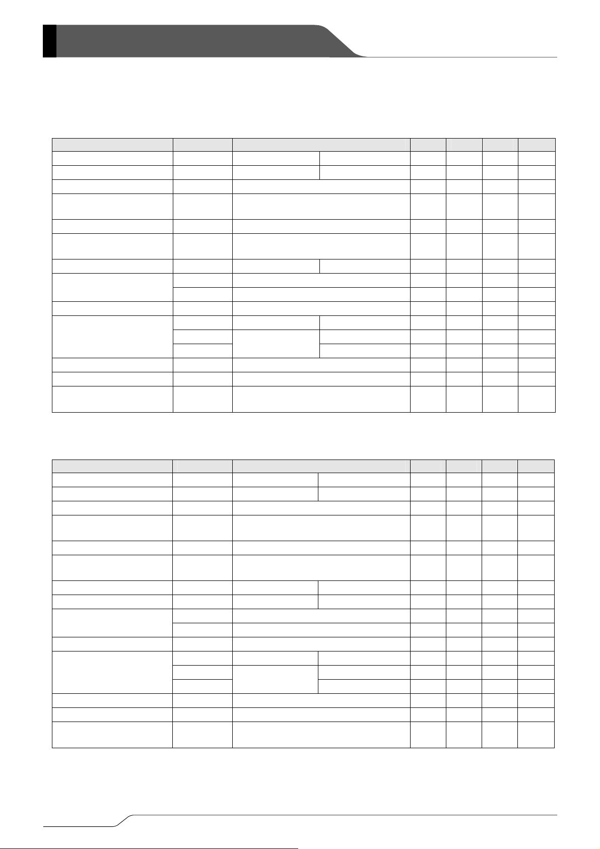
ELECTRICAL CHARACTERISTICS
XC9801B503KR VOUT=5.0V
PARAMETER SYMBOL CONDITIONS MIN. TYP. MAX. UNITS
Output Voltage VOUT Regulation Output IOUT=1mA 4.875 5.000 5.125 V
Load Regulation
△V
OUT
Operating Voltage Range VIN
Supply Current IDD
Regulation Output
Doubler Output, V
1mA≦IOUT≦80mA
OUT>VIN×2×0.95
VIN=3.6V, External Components=CIN only,
SENSE=0V, V
OUT=VIN
Stand-by Current ISTB CE=0V - - 2.0
Oscillation Frequency FOSC
External Component=CIN only,
SENSE=0V, V
OUT open
Output Impedance ROUT Doubler Output IOUT=10mA - 20 40
Input Current
Voltage Converting Efficiency
IIN Doubler Output - 5 - mA
IN2 Regulation Output - 1.5 - mA
I
VEFFI Doubler Output 95 99 - %
EFFI Doubler Output IOUT=10mA 73 78 - %
Power Converting Efficiency
EFFI2 IOUT=1mA - 40 - %
EFFI3
Regulation Output
OUT=80mA 64 69 - %
I
CE / ’H’ Level Voltage VCEH 1.5 - - V
CE / ‘L’ Level Voltage VCEL - - 0.25 V
CE / Input Current ICE
Test Conditions: Unless otherwise stated, Typical Application Circuit, VIN=3.6V,
XC9802B503KR VOUT=5.0V
GND=0V, CE=V
IN, No Load, SENSE=VOUT (Regulation Output)
VIN=5.5V, SENSE=0V,
External Components=C
IN only
PARAMETER SYMBOL CONDITIONS MIN. TYP. MAX. UNITS
Output Voltage VOUT Regulation Output IOUT=1mA 4.875 5.000 5.125 V
Load Regulation
△V
OUT
Operating Voltage Range VIN
Supply Current IDD
Regulation Output
Doubler Output, V
IN=3.6V, External Components=CIN only,
V
SENSE=0V, V
OUT=VIN
1mA≦IOUT≦80mA
OUT >VIN×2×0.95
Stand-by Current ISTB CE=0V - - 2.0
Oscillation Frequency FOSC
Switching Pulse Frequency
FOSC2 Regulation Output IOUT=1mA - 10 - kHz
External Component = C
SENSE=0V, V
OUT open
IN only,
Output Impedance ROUT Doubler Output IOUT=10mA - 20 40
Input Current
Voltage Converting Efficiency
IIN Doubler Output - 5 - mA
IN2 Regulation Output - 0.08 - mA
I
VEFFI Doubler Output 98 99 - %
EFFI Doubler Output IOUT=10mA 73 78 - %
Power Converting Efficiency
CE /HLevel Voltage
CE /LLevel Voltage
CE / Input Current ICE
Test Conditions: Unless otherwise stated, Typical Application Circuit, VIN=3.6V,
GND=0V, CE=V
EFFI2 IOUT=1mA - 59 - %
EFFI3
V
CEH 1.5 - - V
V
CEL - - 0.25 V
Regulation Output
OUT=80mA 64 69 - %
I
VIN=5.5V, SENSE=0V,
External Components=C
IN, No Load, SENSE=VOUT (Regulation Output)
IN only
4/12
-100 - 100 mV
1.8 - 5.5 V
1 3 6 mA
255 300 345 kHz
-2.0 - 2.0
-100 - 100 mV
1.8 - 5.5 V
1 3 6 mA
255 300 345 kHz
-2.0 - 2.0
Ta=25℃
μA
Ω
μA
Ta=25℃
μA
Ω
μA

■
)
XC9801/XC9802
Series
ELECTRICAL CHARACTERISTICS(Continued
XC9801B333KR VOUT=3.3V
PARAMETER SYMBOL CONDITIONS MIN. TYP. MAX. UNITS
Output Voltage VOUT Regulation Output IOUT=1mA 3.218 3.300 3.383 V
Load Regulation
△V
OUT
Operating Voltage Range VIN
Supply Current IDD
Regulation Output
Doubler Output, V
1mA≦IOUT≦2mA
OUT>VIN×2×0.95
VIN=3.6V, External components=CIN only,
SENSE=0V, V
OUT=VIN
-66 - 66 mV
1.8 - 5.5 V
1 3 6 mA
Stand-by Current ISTB CE=0V - - 2.0
Oscillation Frequency FOSC
External component=C
SENSE=0V, V
OUT open
IN only,
255 300 345 kHz
Output Impedance ROUT Doubler Output IOUT=10mA - 20 40
Input Current
IIN Doubler Output - 5 - mA
I
IN2 Regulation Output - 1.1 - mA
Voltage Converting Efficiency VEFFI Doubler Output 95 99 - %
EFFI Doubler Output IOUT=10mA 73 78 - %
Power Converting Efficiency
EFFI2 IOUT=1mA - 40 - %
EFFI3
Regulation Output
OUT=32mA 64 69 - %
I
CE / ‘H’ Level Voltage VCEH 1.5 - - V
CE / ‘L’ Level Voltage VCEL - - 0.25 V
CE / Input Current ICE
Test Conditions: Unless otherwise stated, Typical Application Circuit, VIN=2.376V,
XC9802B333KR VOUT=3.3V
GND=0V, CE=V
IN, No Load, SENSE=VOUT (Regulation Output)
VIN=5.5V, SENSE=0V,
External Components=C
IN only
-2.0 - 2.0
PARAMETER SYMBOL CONDITIONS MIN. TYP. MAX. UNITS
Output Voltage VOUT Regulation Output IOUT=1mA 3.218 3.300 3.383 V
Load Regulation
△V
OUT
Operating Voltage Range VIN
Supply Current IDD
Regulation Output
Doubler Output, V
1mA≦IOUT≦32mA −66
OUT >VIN×2×0.95
VIN=3.6V, External Components=CIN only,
SENSE=0V, V
OUT=VIN
1.8 - 5.5 V
1 3 6 mA
- 66 mV
Stand-by Current ISTB CE=0V - - 2.0
Oscillation Frequency FOSC
External Component = C
SENSE=0V, V
OUT open
IN only,
255 300 345 kHz
Switching Pulse Frequency FOSC2 Regulation Output IOUT=1mA - 10 kHz
Output Impedance ROUT Doubler Output IOUT=10mA - 20 40
Input Current
IIN Doubler Output - 5 - mA
I
IN2 Regulation Output - 0.08 - mA
Voltage Converting Efficiency VEFFI Doubler Output 98 99 - %
EFFI Doubler Output IOUT=10mA 73 78 - %
Power Converting Efficiency
EFFI2 IOUT=1mA - 63 - %
EFFI3
Regulation Output
OUT=32mA 64 69 - %
I
CE / ‘H’ Level Voltage VCEH 1.5 - - V
CE / ‘L’ Level Voltage VCEL - - 0.25 V
CE / Input Current ICE
Test Conditions: Unless otherwise stated, Typical Application Circuit, VIN=2.376V,
GND=0V, CE=V
IN, No Load, SENSE=VOUT (Regulation Output)
VIN=5.5V, SENSE=0V,
External Components=C
IN only
-2.0 - 2.0
Ta=25℃
μA
Ω
μA
Ta=25℃
μA
Ω
μA
5/12

■
XC9801/XC9802 Series
TYPICAL APPLICATION CIRCUITS
① Regulation Output
② Doubler Output
External Components:
CIN=1μF (Ceramic Capacitor: TAIYO YUDEN)
C1=0.47μF (Ceramic Capacitor: TAIYO YUDEN)
C2=4.7μF (Ceramic Capacitor: TAIYO YUDEN)
Note: The XC9801 series are step-up charge pump voltage doublers which provide regulated output voltage.
The application circuit of the doubler output (②) halts the regulated output function and o perates as a normal voltage
doubler.
The output voltage is stable when connected as in (①) above, except when V
IN < (VOUT / 2) and VIN ≧ VOUT.
6/12

■
TYPICAL PERFORMANCE CHARACTERISTICS
●XC9801B333KR (300kHz, 3.3V)
(1) Output Voltage vs. Output Current
(2) Efficiency vs. Output Current
(3) Ripple Voltage vs. Output Current
XC9801/XC9802
Series
7/12

■
●
XC9801/XC9802 Series
TYPICAL PERFORMANCE CHARACTERISTICS (Continued)
XC9801B503KR (300kHz, 5.0V)
(1) Output Voltage vs. Output Current
(2) Efficiency vs. Output Current
(3) Ripple Voltage vs. Output Current
8/12

■
TYPICAL PERFORMANCE CHARACTERISTICS (Continued)
●XC9801B503KR (300kHz, SENSE=0V, Doubler)
(1) Output Voltage vs. Output Current
(2) Efficiency vs. Output Current
(3) Ripple Voltage vs. Output Current
XC9801/XC9802
Series
9/12

■
XC9801/XC9802 Series
PACKAGING INFORMATION
●MSOP-8A
●USP-8 Recommended Pattern Layout ●USP-8 Recommended Metal Mask Design
●USP-8
10/12

■MARKING RULE
●MSOP-8A
XC9801/XC9802
① represents product series
MARK PRODUCT SERIES
2 XC9801Bxx3Kx
3 XC9802Bxx3Kx
② represents true logic level at the CE pin
MARK PRODUCT SERIES
B XC9801/XC9802Bxx3Kx
③④ repres ents output voltage
MARK
③ ④
3 3 3.3 XC9801/XC9802B333Kx
5 0 5.0 XC9801/XC9802B503Kx
⑤ repres ents oscillatio n frequency
MARK OSCILLATION FREQUENCY (kHz) PRODUCT SERIES
3 300 XC9801/XC9802Bxx3Kx
⑥ represents production l ot numb er
0 to 9, A to Z repeated (G, I, J, O, Q, W excluded)
Note: No character inversion used.
VOLTAGE (V) PRODUCT SERIES
Series
11/12

XC9801/XC9802 Series
1. The products and product specifications containe d herein are subject to change without
notice to improve performance characteristics. Consult us, or our representatives
before use, to confirm that the information in this datasheet is up to date.
2. We assume no responsibility for any infringement of patents, patent rights, or other
rights arising from the use of any information and circuitry in this datasheet.
3. Please ensure suitable shipping controls (including fail-safe designs and aging
protection) are in force for equipment employing products listed in this datasheet.
4. The products in this datasheet are not developed, designed, or approved for use with
such equipment whose failure of malfunction can be reasonably expected to directly
endanger the life of, or cause significant injury to, the user.
(e.g. Atomic energy; aerospace; transport; combustion and associated safety
equipment thereof.)
5. Please use the products listed in this datasheet within the specified ranges.
Should you wish to use the products under conditions exceeding the specifications,
please consult us or our representatives.
6. We assume no responsibility for damage or loss due to abnormal use.
7. All rights reserved. No part of this datasheet may be copied or reproduced without the
prior permission of TOREX SEMICONDUCTOR LTD.
12/12
 Loading...