

■
)
XC9519 Series
ETR0710-008
Dual Output Step-Up/Inverting DC/DC Converter
■GENERAL DESCRIPTION
The XC9519 series is a 2 channel (step-up and inverting) DC/DC converter IC. One DC/DC converter is a step-up DC/DC and the other is an
inverting DC/DC converter. The step-up converter compares a built-in reference voltage 1.0V to the FBP voltage (accuracy ±1.5%) and a
positive output voltage can be set freely with the external components up to 18V. The inverting DC/DC converter compares a difference
between a reference voltage and the FBN voltage (accuracy ±1.5%) to the GND, then a negative output voltage can be set until -15V with the
external components.
With a 1.2MHz frequency, the size of the external components can be reduced. As for operation mode, the device can be selected to use PWM
control or automatic PWM/PFM switching control by the MODE pin. In the automatic PWM/PFM switching control mode, control switches from
PWM to PFM during light loads. The series is highly efficient from light loads through to large output currents. In the PWM control mode,
noise is easily reduced since the frequency is fixed. The control mode can be selected for each application. The soft start and current control
functions are internally optimized. During stand-by, all circuits in the IC are shutdown to reduce current consumption to as low as 1.0μA or
less. The device includes a gate control pin for the P-channel MOSFET which is used for a load disconnection at the stand-by mode. The
GAINP and GAINN pins are used for loop compensation in order to optimize load transient response. With the built-in UVLO (Under Voltage
Lock Out) function, the internal driver transistor is forced OFF when input voltage becomes 2.2V or lower.
■APPLICATIONS
●AMOLED
-
Smartphones
-
Tablet PCs
- Automotive navigation systems
●CCD image sensors
-
Surveillance cameras
●e-paper
-e-Books
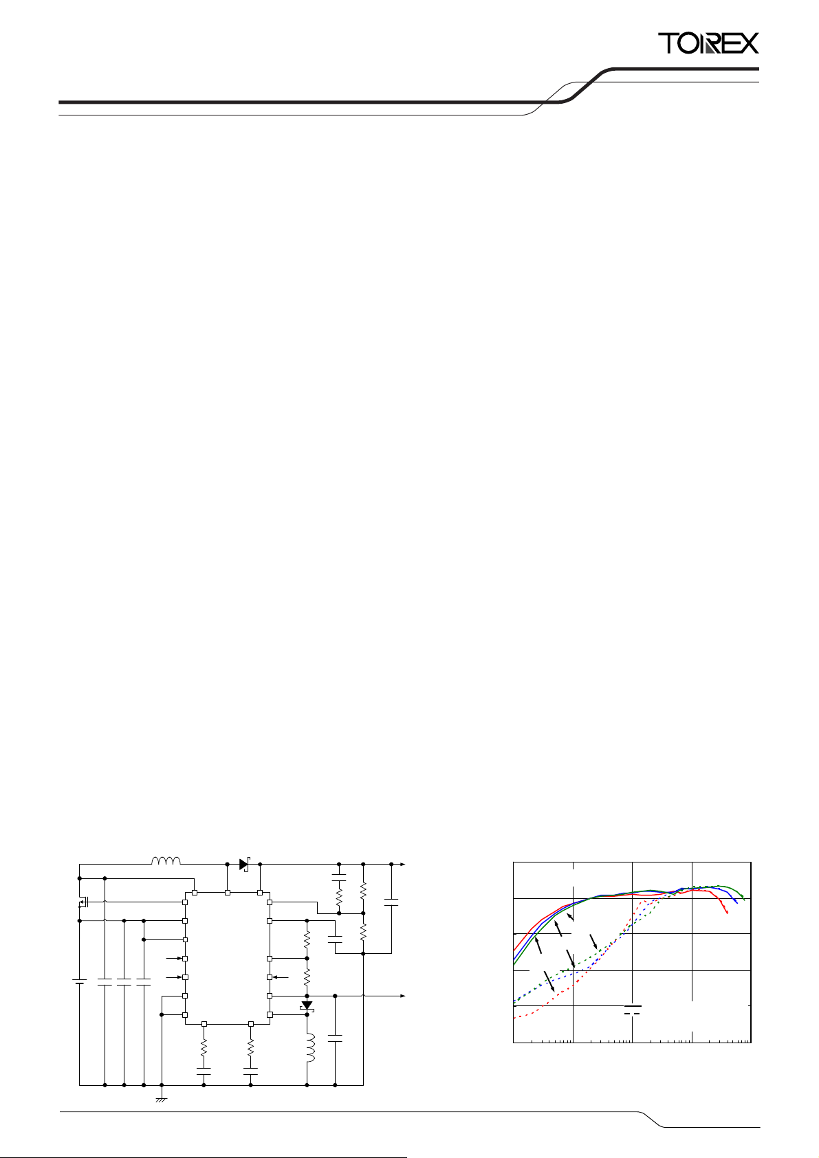
■TYPICAL APPLICATION CIRCUIT
L
P
P-ch MOS
V
C
C
IN
IN_SW
BSW
PVIN
AVIN
ENP FBN
ENN
C
IN_A
IN_P
AGND
PGND
SWP
XC9519
GAINP
R
ZP
C
ZP
LXP
SBD
P
GAINN
R
ZN
C
ZN
VOUTP
FBP
VREF
MODE
VOUTN
LXN
C
FBP
R
FBP1
R
SP
R
C
FBN2
L_VR
R
FBP2
R
FBN1
SBD
N
C
LN
L
N
■FEATURES
Input Voltage : 2.7V ~ 5.5V
Output Current
Positive Output Voltage :
Negative Output Voltage :
: 500mA @VIN=3.7V, V
(*1)
4.0V
~ 18.0V (accuracy ±1.5% @25oC)
(*2)
-15.0V
~ -4.0V (accuracy ±1.5% @25oC)
OUTP
=5.0V, V
OUTN
=-5.0V
Oscillation Frequency : 1.2MHz
Soft-Start Circuit Built-In : Step-up DC/DC converter 2.5ms (TYP.)
:
Inverting DC/DC converter 2.2ms (TYP.)
Protection Circuits : Over Current Limit (Integral Latching)
Short Protection Latching
UVLO
Thermal Shutdown
Over Voltage Protection
Function Addition : Control Pin
Load disconnect Pin
Phase Compensation Pin
Ceramic Capacitor Compatible
Operating Ambient Temperature
: -40℃ ~ +85℃
Package : QFN-24
Environmentally Friendly
(*1)V
OUTPSET≧VIN
(*2)V
(V
- V
IN
: Forward voltage of SBDN, V
FN
OUTNSET
+ 0.2V (V
+ V
≦20V
FN
: EU RoHS Compliant, Pb Free
:Positive output voltage range)
OUTPSET
: Nagative output voltage range)
OUTNSET
TYPICAL PERFORMANCE
CHARACTERISTICS
V
=5.0V, V
OUTP
CLP, CLN=4×4.7μF, LP, LN=3.3μH (VLF5014S-3R3M2R0), SBDP, SBDN: CMS03
V
OUTP
C
LP
V
OUTN
P-ch MOS: EMH1303, RZP=7.5kΩ, CZP=4.7nF, RZN=130kΩ, CZN=0.47nF
100
V
="H",V
ENP
80
60
40
3.6V
2.7V
Efficiency:EFFI(%
20
0
0.1 1 10 100 1000
Output Current:I
OUTN
="H"
ENN
VIN= 4.4 V
=-5.0V, I
OUT P
OUTP=IOUTN
PWM/PFM (V
PWM (V
MODE
, I
(mA)
OUT N
MODE
="L")
="H")
1/38

XC9519 Series
■BLOCK DIAGRAM
* Diodes inside the circuit are an ESD protection diode and a parasitic diode.
■PRODUCT CLASSIFICATION
●Ordering Information
XC9519①②③④⑤⑥-⑦
Internal ON/OFF Controller
DESIGNATOR
①
②③
④
⑤⑥-⑦
(*1)
The “-G” suffix denotes Halogen and Antimony free as well as being fully RoHS compliant.
(*2)
The XC9519 reels are shipped in a moisture-proof packing.
(*1)
UVLO Detect Voltage A
Oscillation Frequency 12 1.2 MHz
Maximum Current Limit A 2.0A
Package (Order Unit) ZR-G QFN-24 (1,000/Reel)
ITEM SYMBOL DESCRIPTION
UVLO Detect Voltage 2.2V
UVLO Hysteresis width 0.2V
2/38
(*2)
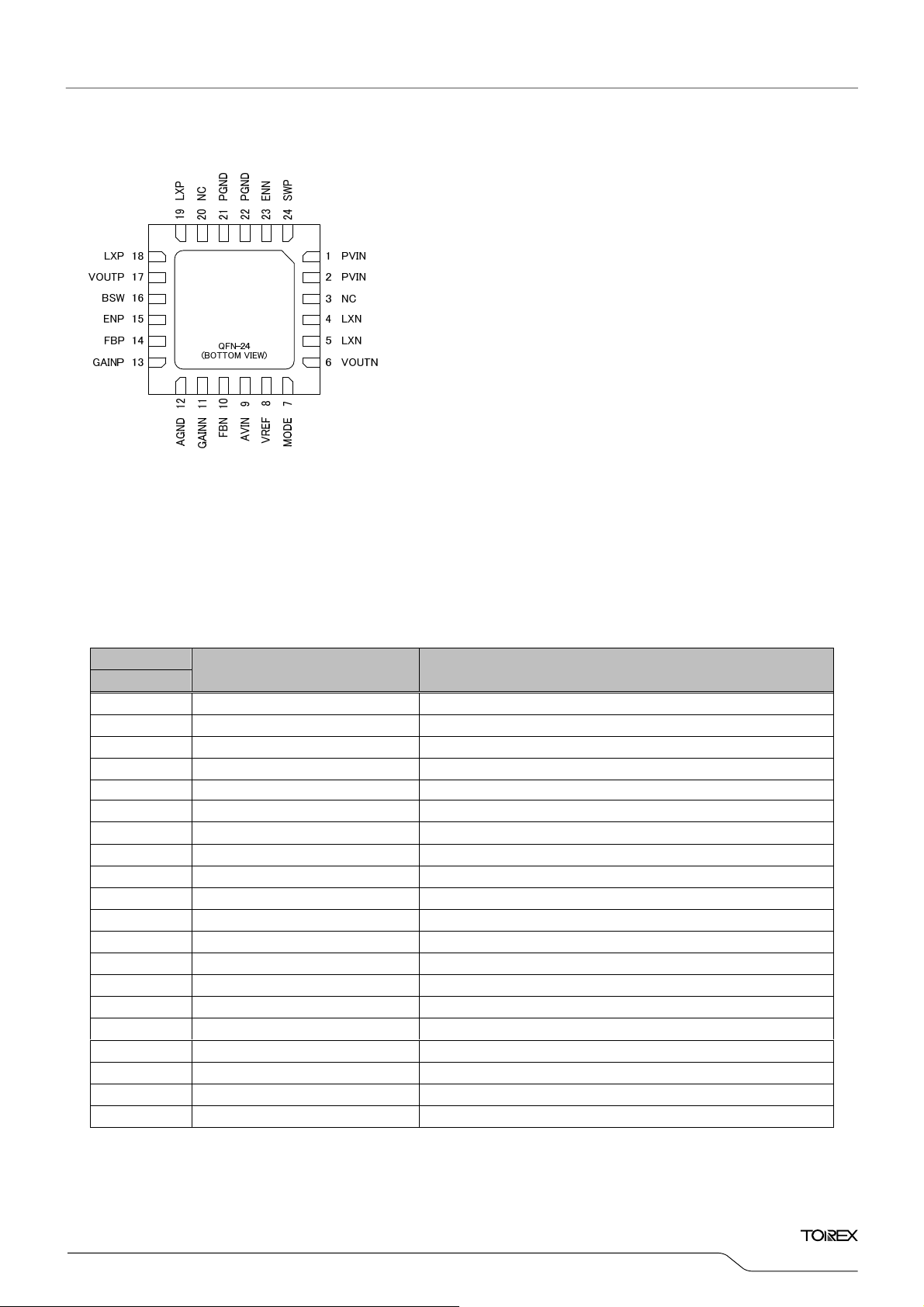
■PIN CONFIGURATION
*1
*1: The back metal pad, AGND pin and two PGND pins (No. 21 and 22) should be connected outside.
■PIN ASSIGNMENT
XC9519
Series
PIN NUMBER
QFN-24
1, 2
3
4, 5
6
7
8
9
10
11
12
13
14
15
16
17
18, 19
20
21, 22
23
24
PIN NAME FUNCTION
PVIN
NC No Connection
LXN Switching of Inverting DC/DC Converter
VOUTN
MODE Selection Pin for Control Mode
VREF Reference Output Voltage
AVIN Power Supply Input 2
FBN Feedback Pin for Inverting DC/DC Converter
GAINN Loop Compensation Pin for Inverting DC/DC Converter
AGND Analog Ground
GAINP Loop Compensation Pin for Step-Up DC/DC Converter
FBP Feedback Pin for Step-Up DC/DC Converter
ENP Chip Enable Pin for Step-Up DC/DC Converter
BSW P-channel MOS FET Gate Control Pin
VOUTP Output Voltage Sense for Step-Up DC/DC Converter
LXP Switching Output of Step-Up DC/DC Converter
NC No Connection
PGND Power Ground
ENN Chip Enable Pin for Inverting DC/DC Converter
SWP Detect Monitoring Voltage Pin for P-channel MOS FET Drain
Power Supply Input 1
Detect Monitoring of Inverting DC/DC Output Voltage
3/38

XC9519 Series
■FUNCTION
1. ENP Pin Function
ENP PIN STATUS
H Step-up DC/DC Converter Active
L Step-up DC/DC Converter Stand-by
* Please do not leave the ENP pin open.
V
IN
ENP
0V
V
IN
BSW
0V
2.5ms
V
OUTP
V
IN
0V
2. ENN Pin Function
ENN PIN STATUS
H Inverting DC/DC Converter Active
L Inverting DC/DC Converter Stand-by
* Please do not leave the ENP pin open.
V
IN
ENN
0V
0V
V
OUTN
3. MODE Pin Function
MODE PIN STATUS
H Auto PWM/PFM
L PWM Control
* Please do not leave the MODE pin open.
2.2ms
4/38
■ABSOLUTE MAXIMUM RATINGS
PAR AMETER SYMBOL RATINGS UNITS
PVIN Pin Voltage V
AVIN Pin Voltage V
ENP Pin Voltage V
ENN Pin Voltage V
MODE Pin Voltage V
LXP Pin Voltage V
LXN Pin Voltage V
FBP Pin Voltage V
FBN Pin Voltage V
VOUTP Pin Voltage V
VOUTN Pin Voltage V
BSW Pin Voltage V
SWP Pin Voltage V
VREF Pin Voltage V
GAINP Pin Voltage V
GAINN Pin Voltage V
LXP Pin Current I
LXN Pin Current I
Power Dissipation Pd 1500 (PCB mounted) * mW
Operating Ambient Temperature Topr -40 ~ +85
Storage Temperature Tstg -55 ~ +125
* All voltages are described based on the AGND and PGND pin.
* The value is an example of data which is taken with the PCB mounted. Please refer to our web site for details.
XC9519
Series
Ta =2 5 ℃
-0.3 ~ +6.0 V
PVIN
-0.3 ~ +6.0 V
AVI N
-0.3 ~ +6.0 V
ENP
-0.3 ~ +6.0 V
ENN
-0.3 ~ +6.0 V
MODE
-0.3 ~ +22.0 V
LXP
V
LXN
-0.3 ~ +6.0 V
FBP
-0.3 ~ +6.0 V
FBN
-0.3 ~ +22.0 V
OUTP
V
OUTN
-0.3 ~ +6.0 V
BSW
-0.3 ~ +6.0 V
SWP
-0.3 ~ +6.0 V
REF
-0.3 ~ +6.0 V
GAINP
-0.3 ~ +6.0 V
GAINN
4000 mA
LXP
4000 mA
LXN
-22.0 ~ V
PVIN
-22.0 ~ V
AVI N
+0.3 V
PVIN
+0.3 V
AVI N
o
C
o
C
5/38
OSC
XC9519 Series
■ELECTRICAL CHARACTERISTICS
●XC9519 Series, Common Characteristics
PARAMETER SYMBOL CONDITIONS
2.7 - 5.5 V -
V
V
UVLO
IN
V
ENP
The voltage which L
V
is decreasing from 2.4V.
IN
=1.5V , V
= V
ENN
= 0V, V
FBP
stops oscillation while
XP
Input Voltage
UVLO Detect Voltage
f
=1.2MHz
(*1)
MIN. TYP. MAX. UNITS CIRCUIT
= 0.1V
FBN
Ta=25℃
2.0 2.2 2.4 V ⑨
UVLO Release Voltage
UVLO Hysteresis Range
Supply Current 1
Supply Current 2
Supply Current 3
Stand-by Current
ENP ”H” Voltage
ENP ”L” Voltage
ENP ”H” Current
ENP ”L” Current
ENN ”H” Voltage
ENN ”L” Voltage
ENN ”H” Current
ENN ”L” Current
MODE ”H” Voltage
MODE ”L” Voltage
MODE ”H” Current
MODE ”L” Current
FBP ”H” Current I
FBP ”L” Current I
FBN ”H” Current I
FBN ”L” Current I
SWP ”H” Current I
SWP ”L” Current I
Integral Latch Time
V
UVLOR
V
V
UVLOH
I
DD1
I
DD2
I
DD3
V
I
STB
V
ENPH
V
ENPL
VIN = V
I
ENPH
VIN = V
I
ENPL
V
ENNH
V
ENNL
VIN = V
I
ENNH
I
VIN = V
ENNL
V
MODEH
V
MODEL
I
VIN = V
MODEH
VIN = V
I
MODEL
VIN =5.5V, V
FBPH
VIN =5.5V, V
FBPL
VIN =5.5V, V
FBNH
VIN =5.5V, V
FBNL
VIN =5.5V, V
SWPH
VIN =5.5V, V
SWPL
t
LAT
=1.5V , V
V
ENP
The voltage which L
V
is increasing from V
IN
= V
UVLOH
V
=V
IN
ENP
V
=5.5V, V
FBP
V
= V
IN
ENN
V
= -0.1V
FBN
V
=V
IN
ENP
V
= 5.5V, V
FBP
=5.5V, V
IN
= 5.5V, V
V
IN
The voltage which L
V
is increasing from 0.3V.
ENP
= 5.5V, V
V
IN
The voltage which L
Is decreasing from 1.4V.
V
ENP
ENP
ENP
= 5.5V, V
V
IN
The voltage which L
V
is increasing from 0.3V.
ENN
= 5.5V, V
V
IN
The voltage which L
V
is decreasing from 1.4V.
ENN
ENN
ENN
= V
V
IN
ENP
The voltage which supply current decreases
while V
MODE
= V
V
IN
ENP
The voltage which supply current increases while
V
is decreasing from 1.4V.
MODE
MODE
MODE
V
=V
IN
ENP =VENN
V
=0.9V, V
FBP
Time to stop operation from the start of maximum
= V
ENN
UVLOR
= V
ENN
FBN
= V
MODE
= V
MODE
OUTP
ENP =VENN
ENN
ENN
= 0V, V
FBP
starts oscillation while
XP
UVLO
- V
- 0.2 - V -
UVLO
= V
= 5.5V
MODE
= -0.1V, V
= 5.5V, V
= 5.5V, V
= V
= 5.5V
SWP
= V
MODE
= V
= 0V, V
MODE
starts oscillation while
XP
= V
= 0V, V
MODE
stops oscillation while
XP
= 0.1V
FBN
2.2 2.4 2.6 V ⑨
.
OUTP
ENP
ENN
= V
= 0V
=0V
SWP
= 5.5V
50 170 450 μA ①
30 90 250 μA ①
30 110 250 μA ①
= 0V - 0 1.0 μA ①
= 0V
FBP
1.4 - 5.5 V ⑦
= 0V
FBP
AGND - 0.3 V ⑦
= 5.5V -0.1 - 0.1 μA ⑦
= 0V -0.1 - 0.1 μA ⑦
= V
ENP
ENP
= 0V, V
MODE
starts oscillation while
XN
= V
= 0V, V
MODE
stops oscillation while
XN
FBN
FBN
= 5.5V
1.4 - 5.5 V ⑦
= 5.5V
AGND - 0.3 V ⑦
= 5.5V -0.1 - 0.1 μA ⑦
= 0V -0.1 - 0.1 μA ⑦
= 5.5V, V
ENN
= 0V,
1.4 - 5.5 V ⑦
is increasing from 0.3V.
= 5.5V, V
ENN
= 0V,
AGND - 0.3 V ⑦
= 5.5V -0.1 - 0.1 μA ⑦
= 0V -0.1 - 0.1 μA ⑦
=V
ENP =VENN
ENP =VENN
ENP =VENN
ENP =VENN
ENP =VENN
ENP =VENN
= 5.5V, V
= 0.1V
FBN
=V
=V
=V
=V
=V
MODE
MODE
MODE
MODE
MODE
MODE
MODE
=0V, V
=0V, V
=0V, V
=0V, V
=0V, V
=0V, V
=0V
=5.5V
FBP
=0V -0.1 - 0.1 μA ⑦
FBP
=5.5V
FBN
=0V -0.1 - 0.1 μA ⑦
FBN
=5.5V
SWP
=0V -0.1 - 0.1 μA ⑦
SWP
-0.1 - 0.1 μA ⑦
-0.1 - 0.1 μA ⑦
-0.1 - 0.1 μA ⑦
1.0 2.0 3.0 ms ⑤
current limit status.
Thermal Shutdown
Temperature
Thermal Shutdown
Release Temperature
Thermal Shutdown
Hysteresis Range
- 150 - oC -
T
TSD
- 130 - oC
T
TSDR
T
T
HYS
HYS
=T
TSDR
- T
- 20 -
TSD
(*1) If the applied voltage and its pin name are not stated, those pins are left open for measurement.
o
C -
-
6/38
■ELECTRICAL CHARACTERISTICS (Continued)
●XC9519 Series, Step-up DC/DC Converter
PARAMETER SYMBOL CONDITIONS
V
Output Voltage Range
FBP Voltage
Oscillation Frequency
PFM Switching Current
Maximum Duty Cycle
LXP SW “H” ON
Resistance
LXP SW “H” Leak
Current
Maximum Current Limit
FBP Voltage
Temperature
(*3)
(V
OUTPSET
V
FBP
f
OSCP
VIN =V
I
PFMP
D
MAXP
VIN = V
R
LXPH
VIN =5.5V, V
I
LEAKH
I
LIMP
V
/
FBP
・
Topr)
FBP
V
= V
= 3.6V, V
IN
ENP
V
= V
SWP
= 3.6V
OUTP
The voltage which L
is decreasing.
V
FBP
V
= V
= 3.6V, V
IN
ENP
V
= V
SWP
= V
ENP
= 3.6V, V
ENP
= V
SWP
= 3.6V, V
ENP
= 5.5V, V
ENP
= 0.9V, V
= 3.6V, V
MODE
= 3.6V, V
=0V, V
ENP
OUTP
V
V
V
V
OUTP
= V
IN
OUTP
=V
IN
FBP
-40 oC≦Topr≦85 oC - ±100 - ppm /
Characteristics
V
= 3.6V, V
Soft-Start Time
IN
V
t
SSP
OUTP
Time to start L
= V
ENN
= 3.6V, V
SWP
XP
(0V→3.6V)
V
=V
= 5.5V, V
IN
Short Protection
Threshold Voltage
V
SHORTP
ENP
V
= V
SWP
= 5.5V
OUTP
The voltage which the integral latch time
becomes 200μs or less while V
V
= V
= 3.6V, V
IN
ENP
V
= V
Over Voltage
Protection Limit
BSW Pin Current
CL Discharge Resistance
V
R
OVPP
I
BSW
DCHGP
OUTP
The voltage which L
V
FBP
V
IN
V
OUTP
V
IN
V
OUTP
= V
= 6.0V, V
= 3.6V, V
SWP
is increasing.
= 3.6V, V
ENP
= V
= 3.6V, V
SWP
ENP =VENN
= 4.0V
ENN
XP
ENN
= 3.6V, V
ENN
ENN
LXP
ENN
= V
SWP
= V
MODE
oscillation from the rise of V
ENN
ENN
XP
ENN
(*1)
MIN. TYP. MAX. UNITS CIRCUIT
= V
= 0V
MODE
starts oscillation while
= V
= 0V
MODE
=0V
FBP
=0V 180 350 550 mA ⑧
ENN
= V
= 0V
MODE
=0V
FBP
= V
MODE
= 0V, I
= 100mA - 0.12 0.28 Ω ④
LXP
=5.5V - 0.01 1.0 μA ⑥
= V
=0V
MODE
= 5.5V
= 0V
= 0.95V
FBP
= V
= V
GAINP
MODE
MODE
= 3.6V
=0V
is decreasing.
FBP
= 0V
ENP
.
stops oscillation while
= V
= 0V
MODE
=3.6V
BSW
= V
= 0V
MODE
XC9519
Series
Ta=25℃
(*2)
4.0
0.985 1.000 1.015 V ③
1020 1200 1380 kHz ③
84 90 97 % ③
2000 - 4000 mA ⑤
0.8 2.5 5.2 ms ③
0.3 0.5 0.7 V ⑤
V
FBP
+0.03
0.2 1.2 3.0 mA ⑦
50 200 500 Ω ②
- 18.0 V -
o
C-
V
+0.07
FBP
V
FBP
+0.10
V ③
NOTE:
(*1) If the applied voltage and its pin name are not stated, those pins are left open for measurement.
(*2) Input voltage or positive output voltage range should be V
OUTPSET≧VIN
+ 0.2V.
(*3) Maximum current limit denotes the level of detection at peak of coil current.
7/38
XC9519 Series
■ELECTRICAL CHARACTERISTICS (Continued)
●XC9519 Series, Inverting DC/DC Converter
PARAMETER SYMBOL CONDITIONS
-15.0
(*3)
V
OUTNSET
= V
V
V
FBN
The voltage which L
V
V
V
REF
V
V
OUTNA
V
f
OSCN
VIN = V
I
PFMN
V
D
MAXN
VIN = V
R
LXNL
V
I
LEAKL
V
I
LIMN
V
REF
(V
・
REF
V
/
-40 oC≦Topr≦85 oC - ±100 - ppm /
To pr )
= 3.6V, V
IN
ENN
is increasing.
FBN
= V
= 3.6V, V
IN
ENN
=V
ENN
ENN
ENN
ENN
ENN
ENN
= 0.1V
-V
REF
= 3.6V, V
= V
= 3.6V, V
= 3.6V, V
= 3.6V, V
= 5.5V, V
OUTNA
= V
IN
= V
IN
= V
IN
= V
IN
FBN
ENP
XN
ENP
0.985 1.000 1.015 V -
FBN
ENP
= 3.6V, V
MODE
ENP
ENP
ENP
ENP
Output Voltage Range
FBN Voltage
Reference Voltage
Output Voltage Accuracy
Oscillation Frequency
PFM Switching Current
Maximum Duty Cycle
LXN SW “L” ON
Resistance
LXN SW “L” Leak
Current
Maximum Current Limit
Reference Voltage
Temperature
Characteristics
Soft-Start Time
t
SSN
= 3.6V, V
V
IN
Time to start L
= V
ENP
MODE
oscillation from the rise of V
XN
(0V→3.6V)
= V
Short Protection
Threshold Voltage
Over Voltage
Protection Limit
CL Discharge Resistance
V
SHORTN
V
R
DCHGN
OVPN
V
IN
The voltage which the integral latch time
becomes 200μs or less while V
V
IN
The voltage which L
V
FBN
V
IN
V
OUTN
= 5.5V, V
ENN
= V
= 3.6V, V
ENN
is decreasing.
= 6.0V, V
ENP =VENN
= -4.0V
ENP
ENP
XN
NOTE:
(*1) If the applied voltage and its pin name are not stated, those pins are left open for measurement.
(*2) Input voltage or positive output voltage range should be V
(*3) Maximum current limit denotes the level of detection at peak of coil current.
IN
8/38
(*1)
MIN. TYP. MAX. UNITS CIRCUIT
= V
= 0V
MODE
starts oscillation while
= V
= 0V, V
MODE
= V
= 0V, V
MODE
= 0V 220 350 550 mA ⑧
ENP
= V
= 0V, V
MODE
= V
= 0V, I
MODE
= V
= 0V, V
MODE
= V
= 0V
MODE
= 0V, V
FBN
= V
= 0V
MODE
FBN
= V
= 0V, V
MODE
= 0.1V 0.970 1.000 1.030 V ①
FBN
= 0.1V 1020 1200 1380 kHz ③
FBN
= 0.1V 84 90 97 % ③
FBN
= 100mA - 0.22 0.48 Ω ④
LXN
= 0.1V - 0.01 1.0 μA ⑥
FBN
= 0.05V
is increasing.
GAINN
stops oscillation while
= V
= 0V
MODE
- V
+ VFN≦20V (VFN: Forward voltage of external schottky barrier diode) .
OUTNSET
ENP
= 3.6V
2000 - 4000 mA ⑤
.
V
-0.10
Ta=25℃
(*2)
- -4.0 V -
-26 0 26 mV ③
o
C -
0.8 2.2 4.0 ms ③
0.3 0.5 0.7 V ⑤
FBN
V
-0.07
FBN
V
FBN
-0.03
V ③
50 200 500 Ω ②
XC9519
Series
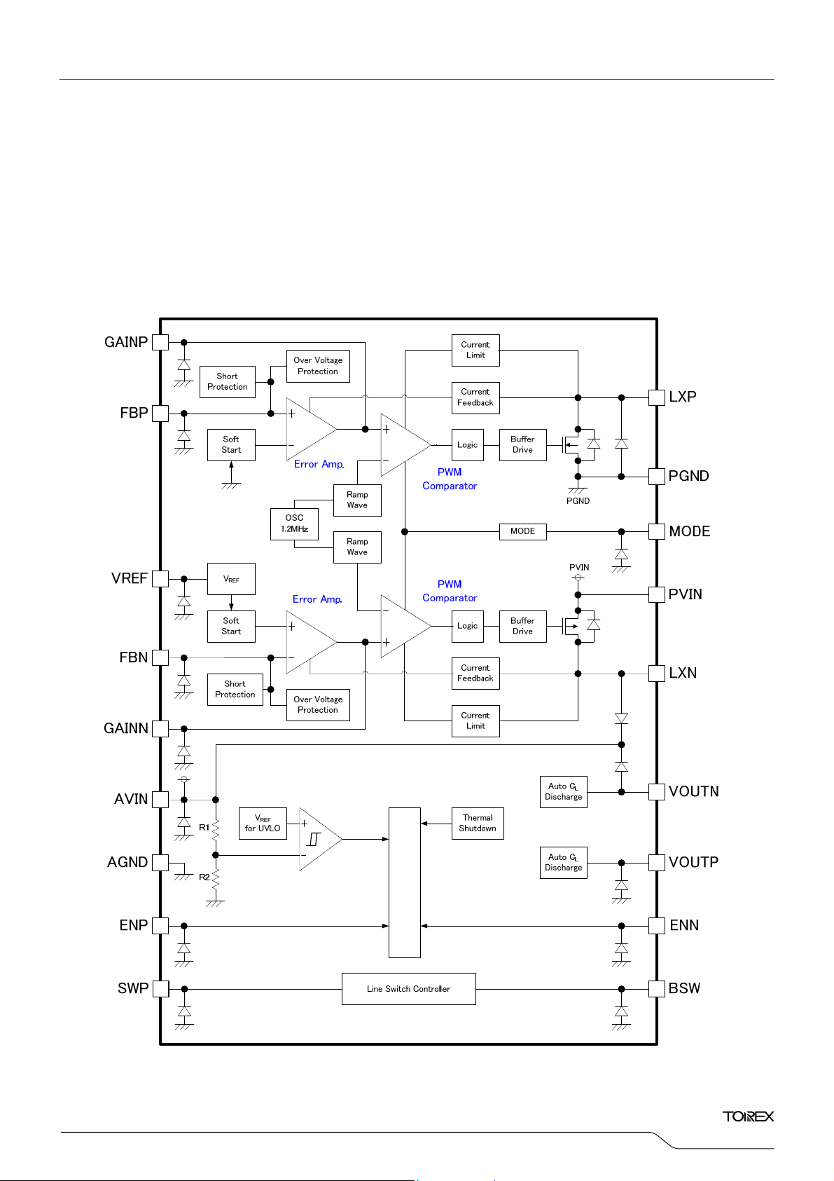
■OPERATIONAL EXPLANATION
The XC9519 series consists of a reference voltage source, ramp wave circuit, error amplifier, PWM comparator, phase compensation circuit,
driver transistor, current limiter circuit, short protection circuit, UVLO circuit, thermal shutdown circuit, over voltage protection, load disconnect
control and others. (See the block diagram below.)
By using the error amplifier, the FBP (FBN) pin voltage is compared with the internal reference voltage. The error amplifier output is sent to the
PWM comparator in order to determine the duty cycle of PWM switching. The signal from the error amplifier is compared with the ramp wave from
the ramp wave circuit, and the resulting output is delivered to the buffer driver circuit to provide on-time of the duty cycle at the LXP (LXN) pin.
This process is continuously performed to ensure stable output voltage.
The current feedback circuit monitors the driver transistor current for each switching operation, and modulates the error amplifier output signal
to provide multiple feedback signals. This enables a stable feedback loop even when using a low ESR capacitor such as ceramic, which results in
ensuring stable output voltage.
* Diodes inside the circuit are an ESD protection diode and a parasitic diode.
Internal ON/OFF Controller
9/38
XC9519 Series
■OPERATIONAL EXPLANATION (Continued)
<Reference Voltage Source>
The reference voltage source provides the reference voltage to ensure stable output voltage of the DC/DC converter.
<Step-up DC/DC Converter Error Amplifier>
The step-up DC/DC converter error amplifier is an amplifier for output voltage monitoring. The FBP pin voltage is compared to the reference
voltage. When a voltage lower than the reference voltage is feedback to the FBP pin voltage, the output voltage of the error amplifier goes high.
External compensation of the error amplifier frequency characteristic is also possible.
<Inverting DC/DC Converter Error Amplifier>
The inverting DC/DC converter error amplifier is an amplifier for output voltage monitoring. The FBN pin voltage is compared to GND. When a
voltage higher than GND is feedback to the FBN pin voltage, the output voltage of the error amplifier goes high. External compensation of the
error amplifier frequency characteristic is also possible.
<Ramp Wave Circuit>
The ramp wave circuit determines switching frequency. The frequency is fixed 1.2MHz internally. Clock pulses generated in this circuit are
used to produce ramp waveforms needed for PWM operation, and to synchronize all the internal circuits.
<UVLO Circuit>
When the AVIN pin voltage becomes 2.2V or lower, the driver transistor is forced OFF to prevent false pulse output caused by unstable
operation of the internal circuitry. When the AVIN pin voltage becomes 2.4V or higher, switching operation takes place. By releasing the UVLO
function, the IC performs the soft start function to initiate output startup operation. The soft start function operates even when the AVIN pin
voltage falls momentarily below the UVLO detect voltage. The UVLO circuit does not cause a complete shutdown of the IC, but causes pulse
output to be suspended; therefore, the internal circuitry remains in operation.
<Thermal Shutdown>
For protection against heat damage of the ICs, thermal shutdown function monitors chip temperature. The thermal shutdown circuit starts
operating and the driver transistor will be turned off when the chip’s temperature reaches 150
after shutting of the current flow, the IC performs the soft start function to initiate output startup operation.
o
C. When the temperature drops to 130 oC or less
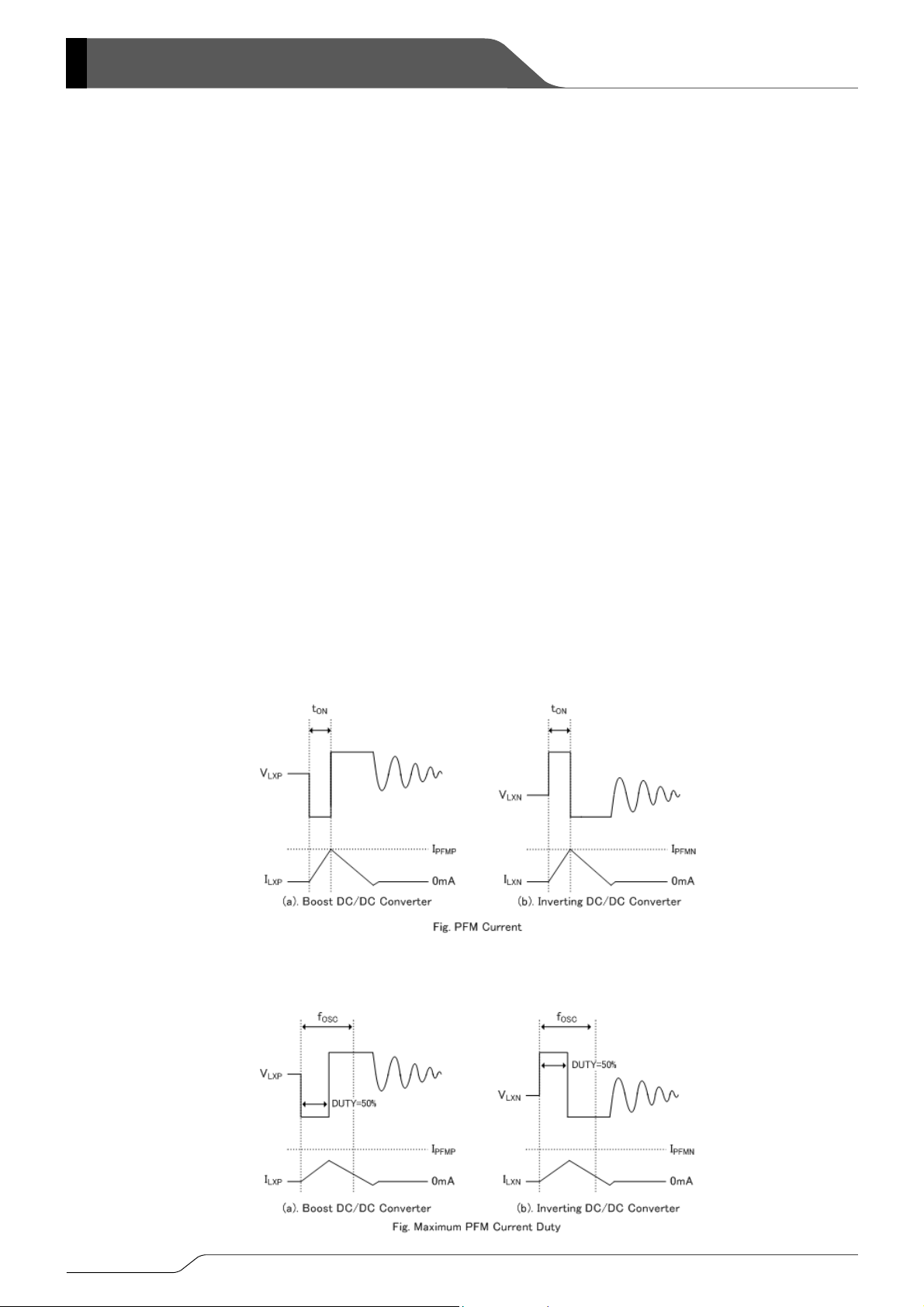
<PFM Switch Current>
, I
In PFM control operation, until coil current reaches to a specified level (I
) that the driver transistor is kept on can be given by the following formula.
(t
ON
t
ON
= L ×I
PFMP
(I
PFMN
) / V
IN
PFMP
), the IC keeps the driver transistor on. In this case, time
PFMN
< PFM Duty Limit >
In PFM control operation, the maximum duty cycle (DTY
(e.g. the condition that the step-up ratio is large), it’s possible for the driver transistor to be turned off even when the coil current doesn’t reach to I
(I
).
PFMN
) is set to 50% (TYP.). Therefore, under the condition that the duty increases
LIMIT_PFM
PFMP
10/38

XC9519
Series
■OPERATIONAL EXPLANATION (Continued)
< CL Auto-Discharge Function >
This function enables high-speed discharge of the charge on the output capacitor (C
means of the internal switch between the VOUTP pin and AGND pin (between the VOUTN pin and AVIN pin).
This function makes it possible to prevent malfunctioning of applications caused by charge remaining on C
The discharge time is determined by the C
discharge resistance (R
L
) and CL. Ifτ(τ= CL × R
DCHC
equation for the output voltage discharge time can be obtained from the following CR discharge equation.
t=τln(
V
OUTSET
/ V)
V: Output voltage during discharge
V
: Output voltage
OUTSET
t: Discharge
τ: C
L×RDCHG
time
[Example]
When the set voltage (V
discharge time t from the start of C
t=τ
ln ( V
(*1) Calculated with I
OUTPSET
/ V )= CLP×R
= 0mA
OUT
)=5.0V, CLP=18.8μF, and the CL discharge resistance (R
OUTPSET
high-speed discharge until the output voltage falls to 1.0V can be calculated as follows:
L
DCHGP
ln ( V
/ V ) = 18.8μF×200Ω×ln ( 5.0V / 1.0V ) = 6.05×10⁻³ s = 6.05 ms
OUTPSET
<Internal OSC Timing Chart>
The step-up DC/DC Converter and the Inverting DC/DC Converter are switching synchronously based on one internal clock. The phase of
the step-up driver on timing for the DC/DC Converter is shifted to completely opposite position (180 degrees different) upon the phase of driver
on timing for the Inverting DC/DC Converter.
) when an L level signal is input to the ENP (ENN) pin by
L
.
L
) is the time constant of CL and R
DCHG
)=200Ω (TYP.) of the DC/DC Converter, the
DCHGP
(*1)
DCHG
, the
Internal OSC
Inductor Peak Current
1.2MHz
Boost_I
LX
Inverting_I
<Overvoltage Protection>
Overvoltage protection monitors the output voltage V
(V
) from rising too far above the set voltage. In particular, fluctuations in the load cause the output voltage to rise, and when the FBP (FBN)
OUTN
pin voltage reaches the overvoltage protection detection voltage, the driver transistor of the step-up DC/DC converter (inverting DC/DC
converter) is turned off to hold down the rise of output voltage. When the output voltage falls after overvoltage protection detection, normal
DC/DC converter operation resumes.
The output voltage V
V
OUT_OVP P (VOUT_OVPN
V
OUTPSET (VOUTNSET
[Example]
In a step-up DC/DC converter with the indicated conditions, the output voltage V
calculated as shown below.
Condition: Output Voltage (V
V
OUT_OVPP
<Load disconnect Control Circuit>
The Load disconnect control circuit makes it possible to break continuity between V
step-up DC/DC converter is in the standby state.
0A
LX
0A
OUT_OVP
)=V
OUTPSET (VOUTNSET
): Output voltage, V
= V
OUTPSET
× V
Inductor Peak Current
(V
OUTP
that is detected by overvoltage protection is obtained from the following equation:
) × V
OVP P (VOVPN
OVPP(VOVPN
OUTPSET
= 5.0V × (1.0 + 0.07(TYP.)) =5.0V × 1.07 = 5.35V
OVP
): Detect Overvoltage Protection Voltage
)=5.0V, V
OVPP=VFBP
) using the FBP (FBN) pin voltage, and prevents the output voltage V
OUTN
)
that is detected by overvoltage protection can be
OUT_OVPP
+0.07V(TYP.) , V
=1.0V(TYP.)
FBP
and V
IN
by turning off the external P-ch MOS FET when the
OUTP
OUTP
11/38

XC9519 Series
■OPERATIONAL EXPLANATION (Continued)
<Current Limit>
The current limiter circuit of the XC9519 series monitors the current flowing through the driver transistor, and features a combination of the
current limit mode and the operation suspension mode.
① When the driver current is greater than a specific level, the current limit function operates to turn off the pulses from the LXP (LXN) pin at any
given timing.
② When the driver transistor is turned off, the limiter circuit is then released from the current limit detection state.
③ At the next pulse, the driver transistor is turned on. However, the transistor is immediately turned off in the case of an over current state.
④ When the over current state is eliminated, the IC resumes its normal operation.
The IC waits for the over current state to end by repeating the steps ① through ③. If an over current state continues for the integral latch time
and the above three steps are repeatedly performed, the IC performs the function of integral latching the OFF state of the driver transistor, and
goes into operation suspension mode.
Once the IC is in suspension mode, operations can be resumed by either turning the IC off via the ENP (ENN) pin, or by restoring power. Care
must be taken when laying out the PC Board, in order to prevent misoperation of the current limit mode. Depending on the state of the PC Board,
latch time may become longer and latch operation may not work. In order to avoid the effect of noise, the board should be laid out so that input
capacitors are placed as close to the IC as possible.
(a) Step-up DC/DC Converter
I
OUTP
V
OUTP
V
LXP
ENP
(b) Inverting DC/DC Converter
I
OUTN
Limit < 2.0ms(TYP.)
Limit < 2.0ms(TYP.)
Limit > 2.0ms(TYP.)
Limit > 2.0ms(TYP.)
Current Limit Level
Restart
Current Limit Level
0mA
AGND,PGND
AGND,PGND
0mA
V
V
ENN
OUTN
LXN
Restart
AGND,PGND
AGND,PGND
<Short-Circuit Protection>
The short-circuit protection circuit monitors the output voltage from the V
OUTP (VOUTN
). In case where output is accidentally shorted to the GND
and when the FBP voltage decreases less than short protection threshold voltage or FBN pin voltage becomes larger than short protection
threshold voltage and a current more than the I
flows to the driver transistor, the short-circuit protection quickly operates to turn off and to latch
LIM
the driver transistor.
Once the IC is in suspension mode, operations can be resumed by either turning the IC off via the ENP (ENN) pin, or by restoring power.
12/38

■EXTERNAL COMPONENTS
<Step-up DC/DC Converter Output Voltage Setting>
The output voltage V
The output voltage V
Adjust R
FBP1
and R
V
= V
FBP
× (R
OUTP
Set the output voltage so that V
Adjust the value of the phase compensation speed-up capacitor C
series as R
. If a high output voltage is set, inserting a phase compensation speed-up capacitor may cause unstable operation.
SP
Examples of setting C
【Typical Examples】
V
R
OUTP
4.0V
5.0V
9.0V
12.0V
15.0V
18.0V
FBP1
300k
300k
240k
330k
336k
408k
<Inverting DC/DC Converter Output Voltage Setting>
The output voltage V
The output voltage V
Adjust R
FBN1
and R
V
= - (V
OUTN
REF
Set the output voltage so that
V
- V
IN
(V
+ V
OUTN
: Forward voltage of external diode SBD
FN
【Typical Examples】
V
R
OUTN
-4.0V
-5.0V
-9.0V
-12.0V
-15.0V
FBN1
300k
300k
270k
360k
360k
of a step-up DC/DC converter can be set by connecting external dividing resistors R
OUTP
is determined by the values of R
OUTP
so that (R
FBP2
+ R
FBP1
and RSP are shown in the next section, “Step-up DC/DC Converter Error Amplifier External Compensation”.
FBP
R
FBP1
) / R
FBP2
OUTP≧VIN
FBP2
+ R
) < 500kΩ.
FBP2
FBP2
+ 0.2V is satisfied.
FBP1
and R
Ω 100kΩ
Ω 75kΩ
Ω 30kΩ
Ω 30kΩ
Ω 24kΩ
Ω 24kΩ
of an inverting DC/DC converter can be set by connecting external dividing resistors R
OUTN
is determined by the values of R
OUTN
so that (R
FBN2
- V
≦
20.0V
FN
R
FBN
) × R
FBN1
FBN2
FBN1
/ R
+ R
FBN2
FBN2
) < 500kΩ.
) is satisfied.
N
FBN1
and R
Ω 75kΩ
Ω 60kΩ
Ω 30kΩ
Ω 30kΩ
Ω 24kΩ
as given in the equation below.
FBP2
so that f
FBP
as given in the equation below.
FBN2
=1 / (2 × π × R
zfp
XC9519
and R
FBP1
) is about 40kHz, and insert several kΩ in
FBP1
FBN1
FBP2
and R
.
FBN2
.
Series
13/38

XC9519 Series
■COMPONENT SELECTION METHOD (Continued)
<Step-up DC/DC Converter Error Amplifier External Compensation>
External compensation of the frequency characteristic of a step-up DC/DC converter error amplifier is possible with R
R
and CZP can be adjusted to obtain the optimum load-transient response (step response). For adjustment using the input voltage and output
ZP
voltage, use the setting values below.
VIN Output Voltage Range LP CLP RZP CZP C
4.7nF 47pF
4.7nF 47pF
4.7nF - -
4.7nF - -
4.7nF - -
2.2nF - -
2.2nF - -
2.2nF - -
2.2nF - -
4.7nF - -
Li-ion
(2.7~4.4V)
4.6V ≦ V
5.0V < V
9.0V < V
12.0V < V
15.0V < V
≦ 5.0V 3.3μH
OUTP
≦ 9.0V 3.3μH
OUTP
≦ 12.0V 3.3μH
OUTP
≦ 15.0V 3.3μH
OUTP
≦ 18.0V 3.3μH
OUTP
2×4.7μF5.1kΩ
4×4.7μF8.2kΩ
2×4.7μF5.1kΩ
×4.7μF7.5kΩ
4
2×4.7μF 10kΩ
4
×4.7μF 18kΩ
2×4.7μF 16kΩ
×4.7μF 27kΩ
4
2×4.7μF 16kΩ
×4.7μF 24kΩ
4
VIN Output Voltage Range LP CLP RZP CZP C
4.7nF 47pF
4.7nF 47pF
2.2nF - -
2.2nF - -
2.2nF - -
2.2nF - -
2.2nF - -
2.2nF - -
2.2nF - -
2.2nF - -
3.3V±10%
4.0V ≦V
5.0V < V
9.0V < V
12.0V < V
15.0V < V
≦ 5.0V 3.3μH
OUTP
≦ 9.0V 3.3μH
OUTP
≦12.0V 3.3μH
OUTP
≦ 15.0V 3.3μH
OUTP
≦ 18.0V 3.3μH
OUTP
2×4.7μF8.2kΩ
×4.7μF 13kΩ
4
2×4.7μF 16kΩ
×4.7μF 22kΩ
4
2×4.7μF 18kΩ
×4.7μF 30kΩ
4
2×4.7μF 24kΩ
4
×4.7μF 36kΩ
2×4.7μF 22kΩ
×4.7μF 36kΩ
4
VIN V
5.7V ≦ V
7.0V < V
5V±10%
9.0V < V
12.0V < V
15.0V < V
LP CLP RZP CZP C
OUTP
≦ 7.0V 3.3μH
OUTP
≦ 9.0V 3.3μH
OUTP
≦ 12.0V 3.3μH
OUTP
≦ 15.0V 3.3μH
OUTP
≦ 18.0V 3.3μH
OUTP
2×4.7μF4.7kΩ
×4.7μF8.2kΩ
4
2×4.7μF5.1kΩ
×4.7μF 10kΩ
4
2×4.7μF8.2kΩ
×4.7μF 16kΩ
4
2×4.7μF 13kΩ
4
×4.7μF 24kΩ
2×4.7μF 12kΩ
×4.7μF 18kΩ
4
4.7nF 68pF
4.7nF 68pF
4.7nF - -
4.7nF - -
4.7nF - -
2.2nF - -
2.2nF - -
2.2nF - -
2.2nF - -
4.7nF - -
(*1) Setting value with RFBP1 = 300kΩ
(*2) Setting value with RFBP1 = 360k
(*3) Setting value with RFBP1 = 240k
Ω
Ω
and CZP. The values of
ZP
RSP
FBP
(*1)
4.7k
(*1)
4.7k
RSP
FBP
(*2)
4.7k
(*2)
4.7k
RSP
FBP
(*3)
4.7k
(*3)
4.7k
Ω
Ω
Ω
Ω
Ω
Ω
14/38

■COMPONENT SELECTION METHOD (Continued)
<Inverting DC/DC Converter Error Amplifier External Compensation>
External compensation of the frequency characteristic of an inverting DC/DC converter error amplifier is possible with R
and CZN can be adjusted to obtain the optimum load-transient response (step response). For adjustment using the input voltage and output
of R
ZN
voltage, use the setting values below.
VIN Output Voltage Range LN CLN RZN CZN
and CZN. The values
ZN
XC9519
Series
2×4.7μF 51kΩ
×4.7μF 110kΩ
4
2×4.7μF 68kΩ
×4.7μF 130kΩ
4
2×4.7μF 120kΩ
×4.7μF 200kΩ
4
2×4.7μF 110kΩ
4
×4.7μF 200kΩ
Li-ion
(2.7~4.4V)
-4.0V≧V
-5.0V > V
-9.0V > V
-12.0V > V
≧-5.0V 3.3μH
OUTN
≧-9.0V 3.3μH
OUTN
≧-12.0V 3.3μH
OUTN
≧ -15.0V 3.3μH
OUTN
1.0nF
0.47nF
0.47nF
0.47nF
0.47nF
0.47nF
1.0nF
0.47nF
VIN Output Voltage Range LN CLN RZN CZN
1.0nF
0.47nF
0.47nF
0.47nF
0.47nF
0.47nF
1.0nF
0.47nF
3.3V±10%
-4.0V≧V
-5.0V > V
-9.0V > V
-12.0V > V
≧-5.0V 3.3μH
OUTN
≧-9.0V 3.3μH
OUTN
≧-12.0V 3.3μH
OUTN
≧-15.0V 3.3μH
OUTN
2×4.7μF 51kΩ
4×4.7μF 110kΩ
2×4.7μF 68kΩ
×4.7μF 130kΩ
4
2×4.7μF 120kΩ
4
×4.7μF 200kΩ
2×4.7μF 110kΩ
×4.7μF 200kΩ
4
VIN Output Voltage Range LN CLN RZN CZN
5V±10%
-4.0V≧V
-5.0V > V
-9.0V > V
-12.0V > V
≧-5.0V 3.3μH
OUTN
≧-9.0V 3.3μH
OUTN
≧-12.0V 3.3μH
OUTN
≧-15.0V 3.3μH
OUTN
2×4.7μF 51kΩ
×4.7μF 110kΩ
4
2×4.7μF 68kΩ
×4.7μF 130kΩ
4
2×4.7μF 120kΩ
×4.7μF 200kΩ
4
2×4.7μF 110kΩ
4
×4.7μF 200kΩ
1.0nF
0.47nF
0.47nF
0.47nF
0.47nF
0.47nF
1.0nF
0.47nF
15/38

XC9519 Series
■TYPICAL APPLICATION CIRCUIT
(V
=3.6V, V
IN
OUTP
=5.0V, V
OUTN
=-5.0V)
<Typical Examples> V
=3.6V, V
IN
OUTP
=5.0V, V
OUTN
=-5.0V
・ Capacitor
C
C
C
C
C
C
C
C
C
For C
minimal reduction of capacitance when a DC bias is applied.
IN_P
IN_SW
IN_A
LP
LN
L_VR
: 4.7nF/ 25V (C1005JB1E472K, TDK-EPC)
ZP
: 0.47nF/ 50V (C1005JB1H471K, TDK-EPC)
ZN
: 47pF/ 50V (C1005CH1H470J, TDK-EPC)
FBP
IN_P, CIN_SW
μF/ 10V (C2012JB1A106M, TDK-EPC)
: 10
μF/ 10V (C2012JB1A475M, TDK-EPC)
: 4.7
μF/ 10V (C1005JB1A104K, TDK-EPC)
: 0.1
μF/ 10V (C2012JB1A475M, TDK-EPC)
: 4×4.7
μF/ 10V (C2012JB1A475M, TDK-EPC)
: 4×4.7
μF/ 6.3V (C1005JB0J224M, TDK-EPC)
: 0.22
, C
, C
IN_A
, CLP, and CLN, use a B characteristic (JIS Standards) or X7R/X5R (EIA Standards), and use a ceramic capacitor with
L_VR
・ Coil, Schottky diode, P-ch MOSFET
L
SBD
P, LN
μH (VLF5014S-3R3M2R0, TDK-EPC)
: 3.3
(MSS5121-332, Coilcraft)
SBDN : XBS304S17R-G (TOREX)
P,
CMS03 (TOSHIBA)
P-ch MOS : EMH1303 (SANYO)
When selecting external components, refer to the specifications of each component and select so as not to exceed the ratings.
・
Resistor
R
R
R
FBP1
FBP2
SP
: 300k
: 75k
: 4.7k
Ω
Ω
Ω
R
R
FBN1
FBN2
: 300k
: 60k
Ω
Ω
R
R
ZP
ZN
: 8.2k
: 110k
Ω
Ω
16/38

■TYPICAL APPLICATION CIRCUIT (Continued)
(V
=3.6V, V
IN
OUTP
=15.0V, V
OUTN
=-15.0V)
XC9519
Series
<Typical Examples> V
=3.6V, V
IN
OUTP
=15.0V, V
OUTN
=-15.0V
・Capacitor
C
C
C
C
C
C
C
C
C
IN_P
IN_SW
IN_A
LP
LN
L_VR
: 2.2nF/ 50V (C1005JB1H222K, TDK-EPC)
ZP
: 0.47nF/ 50V (C1005JB1H471K, TDK-EPC)
ZN
: OPEN
FBP
For C
IN_P, CIN_SW
use a ceramic capacitor with minimal reduction of capacitance when a DC bias is applied.
μF/ 10V (C2012JB1A106M, TDK-EPC)
: 10
μF/ 10V (C2012JB1A475M, TDK-EPC)
: 4.7
μF/ 10V (C1005JB1A104K, TDK-EPC)
: 0.1
μF/ 25V (TMK212BJ475KG, TAIYO YUDEN)
: 4×4.7
μF/ 25V (TMK212BJ475KG, TAIYO YUDEN)
: 4×4.7
μF/ 6.3V (C1005JB0J224M, TDK-EPC)
: 0.22
, C
, C
IN_A
, CLP, and CLN, use a B characteristic (JIS Standards) or X7R/X5R (EIA Standards), and
L_VR
・ Coil, Schottky diode, P-ch MOSFET
L
SBD
P, LN
μH (VLF5014S-3R3M2R0, TDK-EPC)
: 3.3
(MSS5121-332, Coilcraft)
SBDN : XBS304S17R-G (TOREX)
P,
CMS03 (TOSHIBA)
P-ch MOS : EMH1303 (SANYO)
When selecting external components, refer to the specifications of each component and select so as not to exceed the ratings.
・
Resistor
R
R
R
FBP1
FBP2
: OPEN
SP
: 336k
: 24k
Ω
Ω
R
R
FBN1
FBN2
: 360k
: 24k
Ω
Ω
R
R
ZP
ZN
: 27k
: 200k
Ω
Ω
17/38

XC9519 Series
■TEST CIRCUITS
1) Circuit ① 2) Circuit ②
3) Circuit ③
1μF
V
4) Circuit ④
Wave Form Measure Point
ENP
ENN
MODE
SWP
BSW
PVIN
AVIN
AGND
PGND
IN
LXP
VOUTP
FBP
VREF
FBN
VOUTN
LXN
GAINN
GAINP
0.22μF
47Ω
Wave Form Measure Point
47Ω
100kΩ
V
18/38
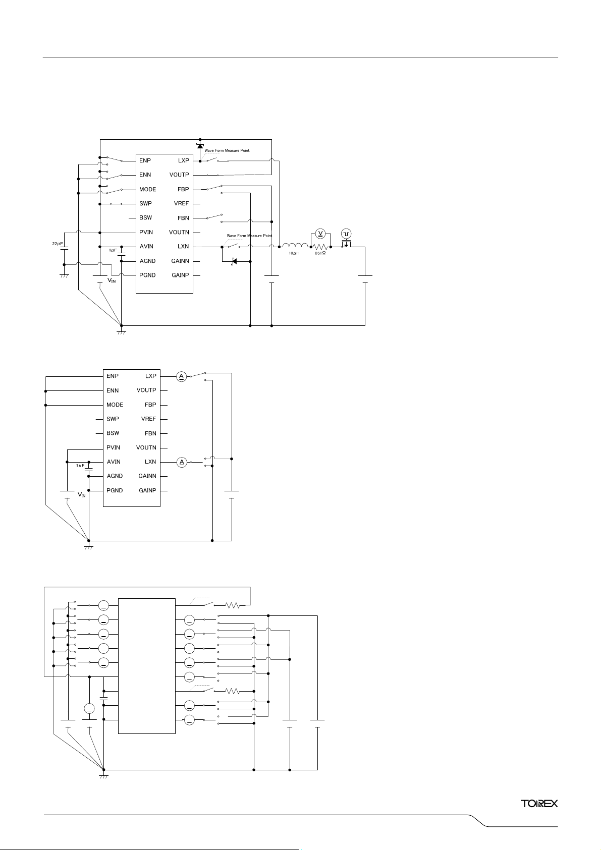
■TEST CIRCUITS (Continued)
5) Circuit ⑤
XC9519
Series
6) Circuit ⑥
7) Circuit ⑦
ENP
A
ENN
A
MODE
A
SWP
A
BSW
A A
PVIN
1μF
A
AVIN
AGND
PGND
V
IN
VOUTP
VOUTN
GAINN
GAINP
LXP
FBP
VREF
FBN
LXN
Wave Form Measure Point
A
A
A
A
Wave Form Measure Point
A
A
47Ω
47Ω
19/38

XC9519 Series
■TEST CIRCUITS (Continued)
8) Circuit ⑧
9) Circuit ⑨
1. Capacitance between pins
The capacitances between the following pins are omitted in the circuit diagram.
PVIN pin – PGND pin: 1μF
FBP pin - AGND pin: 1μF
FBN pin - AGND pin: 1μF
VREF pin - AGND pin: 1μF
2. Testing method for on resistance
Testing is executed at 100% DUTY using test mode.
20/38

XC9519
Series
■NOTES ON USE
1. For temporary, transitional voltage drop or voltage rising phenomenon, the IC is liable to malfunction should the ratings be exceeded.
2. The characteristics of this IC are highly dependent on peripheral circuits.
When selecting external components, refer to the specifications of each component and select so as not to exceed the ratings.
Some peripheral component selections may cause unstable operation.
Before use, sufficiently test operation using the actual equipment.
3. When the input voltage V
is low and the output voltage V
IN
OUTP/VOUTN
the set output voltage may not be output.
4. If the step-up ratio is high and excessive load current flows, the input current may be limited by the maximum duty limit and maximum current
limit protection and short-circuit protection may not activate.
5. Do not connect a component other than C
If a component other than C
is connected, the output voltage V
L_VR
to the VREF pin.
L_VR
6. For external components, use the components specified in the standard circuit examples and component selection methods.
7. When the input voltage VIN is high and the output voltage V
OUTP/VOUTN
8. If the step-up ratio is low in a step-up DC/DC converter, the output voltage V
= "H").
(V
MODE
Step-up DC/DC Converter: PWM/PFM MODE
(V
=4.4V, V
IN
V
="H", V
ENP
OUTP
ENN
=5.0V, I
="L", V
OUTP
MODE
=200mA
="H")
<External Components >
=4×4. 7μF
C
LP
=3. 3μH (VLF 5014S-3R 3M2R0)
L
P
: CMS03
SBD
P
P-ch MOS: EMH1303
=7. 5k Ω, CZP=4.7nF
R
ZP
V
OUT P
:50mV/div
time:20μs/div
9. During PFM/PWM switching control (V
= "H"), the output voltage may become unstable near switching between PFM mode and PWM mode.
MODE
Step-up DC/DC Converter: PWM/PFM MODE
(V
=3.6V, V
IN
V
="H", V
ENP
OUTP
ENN
=5.0V, I
="L", V
OUTP
MODE
=120mA
="H")
<External Com ponents >
=4×4. 7μF
C
LP
=3. 3μH (VLF5014S-3R3M2R0)
L
P
: CMS03
SBD
P
P-ch MOS: EMH1303
=7. 5k Ω, CZP=4.7 nF
R
ZP
is high, the input current may be limited by the maximum duty limit and
of an inverting DC/DC converter may become unstable.
OUTN
is low, intermittent oscillation may occur during PWM control.
may become unstable during PFM/PWM switching control
OUTP
time:10μs/div
V
OUT P
:20mV/div
21/38

XC9519 Series
■NOTES ON USE (Continued)
10. During PWM control (V
Inverting DC Converter: PWM MODE
(V
=5.5V, V
IN
V
="L", V
ENP
OUTN
ENN
=-15.0V, I
="H", V
time:50μs/div
11. Torex places an importance on improving our products and their reliability.
We request that users incorporate fail-safe designs and post-aging protection treatment when using Torex products in their systems.
= "L"), the output voltage may become unstable at light loads.
MODE
<External Components >
=4×4. 7μF
C
LN
=3. 3μH (VLF 5014S-3R 3M2R0)
L
N
: CMS03
SBD
N
R
=200kΩ , CZN=0.47nF
ZN
MODE
OUTN
="L")
=100mA
V
OUT N
:20mV/div
22/38
XC9519
Series
■NOTES ON USE (Continued)
●Notes on Layout
1. Position external components close to the IC so that the wiring is thick and short.
2. To minimize input voltage fluctuations, place C
3. Make the GND wiring sufficiently strong. Fluctuations of AGND or PGND voltage due to GND current during switching may cause unstable IC operation.
4. When creating a layout, refer to the circuit diagram and recommended layout pattern below.
5. This product is incorporated into a driver, and thus the driver transistor current and on-resistance may cause heat generation.
SBD
L
P
P-ch MOS
SWP
BSW
PVIN
AVIN
V
IN
C
C
IN_SW
ENP
C
IN_A
IN_P
ENN
AGND
PGND
GAINP
R
ZP
C
ZP
P
LXP
GAINN
R
C
ZN
ZN
IN_P
VOUTP
FBP
VREF
FBN
MODE
VOUTN
LXN
and C
R
FBP1
as close as possible to the IC.
IN_A
V
OUTP
C
FBP
C
LP
R
SP
R
FBP2
R
FBN2
C
R
FBN1
SBD
L
L_VR
V
OUTN
N
C
LN
N
●Recommended Pattern Layout
Front Back side see-through
23/38
)
)
)
)
XC9519 Series
■TYPICAL PERFORMANCE CHARACTERISTICS
(1)
Efficiency vs. Output Current
100
Step-up DC/DC Converter (V
C
=4×4.7μF, LP=3.3μH (VLF5014S-3R3M2R0)
LP
SBDP: CMS03, P-ch MOS: EMH1303, RZP=7.5kΩ, CZP=4.7nF
V
="H",V
ENN
="L"
ENP
OUTP
=5.0V)
Inverting DC/DC Converter (V
C
LN
100
V
="L", V
ENN
="H"
ENP
=-5.0V)
=4×4.7μF, LN=3.3μH (VLF5014S-3R3M2R0)
SBDN: CMS03, RZN=130kΩ, CZN=0.47nF
OUTN
80
60
40
2.7V
VIN= 4.4V
3.6V
Efficiency:EFFI(%
20
0
0.1 1 10 100 1000
Output Current:I
100
Efficiency:EFFI(%
Step-up DC/DC Converter (V
C
=4×4.7μF, LP=3.3μH (VLF5014S-3R3M2R0)
LP
SBDP: CMS03, P-ch MOS: EMH1303, RZP=27kΩ, CZP=2.2nF
V
="H", V
ENP
80
60
40
20
0
0.1 1 10 100 1000
="L"
ENN
VIN= 5.5V
3.6V
Output Current:I
(2) Output Voltage vs. Output Current
5.2
5.1
(V)
OUTP
Step-up DC/DC Converter (V
C
=4×4.7μF, LP=3.3μH (VLF5014S-3R3M2R0)
LP
SBDP: CMS03, P-ch MOS: EMH1303, RZP=7.5kΩ, CZP=4.7nF
V
ENP
="H",V
ENN
="L"
V
4.4V,3. 6V,2. 7V
=
IN
PWM/PFM (V
PWM (V
MODE
(mA)
OUT P
OUTP
PWM/PFM (V
PWM (V
MODE
(mA)
OUTP
OUTP
="H")
MODE
="L")
=15.0V)
="H")
MODE
="L")
=5.0V)
80
60
40
2.7V
VIN= 4.4V
3.6V
Efficiency:EFFI(%
20
PWM/PF M (V
PWM (V
0
0.1 1 10 100 1000
Output Current:I
Inverting DC/DC Converter (V
C
=4×4.7μF, LN=3.3μH (VLF5014S-3R3M2R0)
LN
100
V
="L", V
ENN
="H"
ENP
SBDN: CMS03, RZN=200kΩ, CZN=0.47nF
OUTN
(mA)
OUTN
80
60
3.6V
40
Efficiency:EFFI(%
20
VIN= 5.5V
PWM/PF M (V
PWM (V
0
0.1 1 10 100 1000
Output Current:I
Inverting DC/DC Converter (V
C
=4×4.7μF, LN=3.3μH (VLF5014S-3R3M2R0)
LN
-4.8
V
="L",V
ENP
(V)
-4.9
OUTN
SBDN: CMS03, RZN=130kΩ, CZN=0.47nF
="H"
ENN
OUTN
3.6V
(mA)
OUTN
="L")
MODE
=-15.0V)
MODE
="L")
MODE
=-5.0V)
V
IN
MODE
=
="H")
="H")
4.4V
5.0
4.9
Output Voltage:V
PWM/PFM (V
PWM (V
MODE
MODE
="L")
="H")
4.8
0.1 1 10 100 1000
Output Current:I
OUTP
(mA)
Output Voltage:V
-5.0
2.7V
-5.1
PWM/PFM (V
PWM (V
-5.2
MODE
MODE
="L")
0.1 1 10 100 1000
Output Current:I
OUTN
(mA)
="H")
24/38

)
)
)
■TYPICAL PERFORMANCE CHARACTERISTICS (Continued)
(2) Output Voltage vs. Output Current (Continued)
Step-up DC/DC Converter (V
C
=4×4.7μF, LP=3.3μH (VLF5014S-3R3M2R0)
LP
15.4
SBDP: CMS03, P-ch MOS: EMH1303, RZP=27kΩ, CZP=2.2nF
V
="H", V
ENN
="L"
ENP
OUTP
=15.0V
Inverting DC/DC Converter (V
C
=4×4.7μF, LN=3.3μH (VLF5014S-3R3M2R0)
LN
-14.6
V
="L", V
ENN
="H"
ENP
OUTN
SBDN: CMS03, RZN=200kΩ, CZN=0.47nF
XC9519
Series
=-15.0V
15.2
(V)
OUTP
15.0
3.6V
14.8
Output Voltage:V
14.6
0.1 1 10 100 1000
Output Current:I
(3) Ripple Voltage vs. Output Current
100
Ripple Voltage : Vr(mVp-p)
Step-up DC/DC Converter (V
C
=4×4.7μF, LP=3.3μH (VLF5014S-3R3M2R0)
LP
SBDP: CMS03, P-ch MOS: EMH1303, RZP=7.5kΩ, CZP=4.7nF
V
="H",V
ENN
="L"
4.4V
3.6V
2.7V
ENP
80
60
40
VIN= 2.7V,3. 6V,4.4V
20
V
5.5V
=
IN
PWM/PF M (V
PWM (V
(mA)
OUTP
PWM/PF M (V
PWM (V
MODE
OUTP
MODE
="H")
MODE
="L")
=5.0V)
="H")
MODE
="L")
(V)
OUTN
Output Voltage:V
100
Ripple Voltage : Vr(mVp-p)
-14.8
V
V,3.6V
=5.5
IN
-15.0
-15.2
PWM/PF M (V
PWM (V
-15.4
MODE
0.1 1 10 100 1000
Output Current:I
Inverting DC/DC Converter (V
C
=4×4.7μF, LN=3.3μH (VLF5014S-3R3M2R0)
LN
SBDN: CMS03, RZN=130kΩ, CZN=0.47nF
V
="L", V
ENN
="H"
ENP
(mA)
OUTN
OUTN
PWM/PF M (V
PWM (V
MODE
80
60
4.4V
40
VIN= 2.7V,3. 6V,4.4V
20
2.7V
3.6V
="H")
MODE
="L")
=-5.0V)
="H")
MODE
="L")
0
0.1 1 10 100 1000
Output Current:I
OUTP
(mA)
0
0.1 1 10 100 1000
Output Current:I
OUTN
(mA)
100
Ripple Voltage : Vr(mVp-p)
Step-up DC/DC Converter (V
C
=4×4.7μF, LP=3.3μH (VLF5014S-3R3M2R0)
LP
SBDP: CMS03, P-ch MOS: EMH1303, RZP=27kΩ, CZP=2.2nF
V
="H",V
ENP
="L" PWM/PF M (V
ENN
PWM (V
OUTP
MODE
=15.0V
="H")
MODE
="L")
80
60
5.5V
40
VIN= 2.7V,3. 6V,4.4V
2.7V
3.6V
20
0
0.1 1 10 100 1000
Output Current:I
OUTP
(mA)
Inverting DC/DC Converter (V
C
=4×4.7μF, LN=3.3μH (VLF5014S-3R3M2R0)
LN
100
V
="L", V
ENN
="H"
ENP
SBDN: CMS03, RZN=200kΩ, CZN=0.47nF
OUTN
PWM/PFM (V
PWM (V
80
60
VIN= 5.5V
40
20
Ripple Voltage : Vr(mVp-p)
2.7V
3.6V
0
0.1 1 10 100 1000
Output Current:I
OUTN
(mA)
MODE
=-15.0V)
="H")
MODE
="L")
25/38

XC9519 Series
■TYPICAL PERFORMANCE CHARACTERISTICS (Continued)
(4) Oscillation Frequency vs. Ambient Temperature
1.5
1.4
(MHz)
OSC P
1.3
VIN=5. 5V3.6V
1.2
1.1
2.7V
1.0
Os c illation Frequency : f
0.9
-50 -25 0 25 50 75 100
Ambient Temperature: Ta (℃)
(5) Supply Current 1,2,3 vs. Ambient Temperature
250
A)
200
μ
(
DD1
Supply Current 1 Supply Current 2
VIN=5.5V
1.5
1.4
(MHz)
OSC N
1.3
VIN=5.5V3.6V
1.2
1.1
2.7V
1.0
Oscillation Frequenc y : f
0.9
-50 -25 0 25 50 75 100
Ambient Temperature: Ta (℃)
200
A)
150
μ
(
DD2
VIN=5. 5V
150
2.7V
100
Supply Current 1: I
50
-50 -25 0 25 50 75 100
Ambient Temperature: Ta (
Supply Current 3
℃
)
100
50
Supply Current 2: I
0
-50 -25 0 25 50 75 100
Ambient Temperature: Ta (
2.7V
℃
)
200
A)
μ
(
150
DD3
VIN=5.5V
100
2.7V
50
Supply Current 3: I
0
-50 -25 0 25 50 75 100
Ambient Temperature: Ta (
℃
)
26/38

■TYPICAL PERFORMANCE CHARACTERISTICS (Continued)
(6) FBP Voltage vs. Ambient Temperature (7) Output Voltage Accuracy vs. Ambient Temperature
XC9519
Series
1.02
VIN=5.5V
1.01
(V)
FBP
1.00
2.7V,3. 6V
0.99
FBP Voltage : V
0.98
-50 -25 0 25 50 75 100
Ambient Temperature: Ta (
(8) UVLO Voltage vs. Ambient Temperature
2.7
2.6
2.5
2.4
UVLO R elease Voltage
℃
1.02
(V)
VIN=5.5V
OUTN A
1.01
1.00
2.7V
3.6V
Output Voltage Accuracy : V
0.99
0.98
-50 -25 0 25 50 75 100
)
Ambient Temperature: Ta (℃)
2.3
2.2
UVLO Detect Voltage
UVLO Voltage : UVLO (V)
2.1
V
="H", V
ENP
ENN
2.0
-50-25 0 25 50 75100
Ambient Temperature: Ta (
(9) ENP "H" Voltage vs. Ambient Temperature
1.4
1.3
(V)
1.2
ENPH
1.1
1.0
0.9
ENP "H" Voltage : V
0.8
VIN=5.5V, V
ENN
0.7
-50-25 0 255075100
Ambient Temperature: Ta (
="L", V
℃
="L", V
℃
)
)
MODE
MODE
="L"
="L"
(10) ENP "L" Voltage vs. Ambient Temperature
1.2
1.1
(V)
1.0
ENPL
0.9
0.8
0.7
ENP "L" Voltage : V
0.6
0.5
-50 -25 0 25 50 75 100
Ambient Temperature: Ta (
VIN=5. 5V, V
ENN
="L",V
℃
="L"
MODE
)
27/38

XC9519 Series
■TYPICAL PERFORMANCE CHARACTERISTICS(Continued)
(11) ENN "H" Voltage vs. Ambient Temperature
1.4
(12) ENN "L" Voltage vs. Ambient Temperature
1.2
1.3
(V)
1.2
ENNH
1.1
1.0
0.9
ENN "H" Voltage : V
0.8
VIN=5.5V, V
ENP
="L", V
0.7
-50 -25 0 25 50 75 100
Ambient Temperature: Ta (
℃
(13) MODE "H" Voltage vs. Ambient Temperature
1.4
1.3
(V)
1.2
MODEH
1.1
MODE
)
="L"
1.1
(V)
1.0
ENNL
0.9
0.8
0.7
ENN "L" Voltage : V
0.6
VIN=5. 5V, V
ENP
="L",V
MODE
0.5
-50 -25 0 25 50 75 100
Ambient Temperature: Ta (
℃
)
(14) MODE "L" Voltage vs. Ambient Temperature
1.2
1.1
(V)
1.0
MODEL
0.9
="L"
1.0
0.9
0.8
MODE "H" Voltage : V
VIN=5. 5V, V
ENP
="H", V
ENN
="L"
0.7
-50 -25 0 25 50 75 100
Ambient Temperature: Ta (
℃
)
(15) LXP SW “H” ON Resistance vs. Ambient Temperature
0.3
(Ω)
LXPH
0.2
2.7V
0.1
3.6V
VIN=5. 5V
LXP SW “H” ON Res istanc e :R
0.0
-50 -25 0 25 50 75 100
Ambient Temperature: Ta (
℃
)
0.8
0.7
0.6
MODE "L" Voltage : V
VIN=5. 5V, V
ENP
="H", V
ENN
="L"
0.5
-50 -25 0 25 50 75 100
Ambient Temperature: Ta (
℃
)
(16) LXN SW "L" ON Resistance vs. Ambient Temperature
0.5
(Ω)
0.4
LXNL
0.3
0.2
0.1
LXN SW “L” ON Resistance :R
0.0
-50 -25 0 25 50 75 100
Ambient Temperature: Ta (
2.7V
3.6V VIN=5. 5V
℃
)
28/38

)
■TYPICAL PERFORMANCE CHARACTERISTICS (Continued)
(17) Output Voltage Rise Wave Form
Step-up DC/DC Converter (V
C
=4×4.7μF, LP=3.3μH (VLF5014S-3R3M2R0)
LP
SBDP: CMS03, P-ch MOS: EMH1303, RZP=27kΩ, CZP=2.2nF
VIN=3.6V,V
ENN
="L",V
MODE
="L"
OUTP
=15.0V
Inverting DC/DC Converter (V
C
=4×4.7μF, LN=3.3μH (VLF5014S-3R3M2R0)
LN
SBDN: CMS03, RZN=200kΩ, CZN=0.47nF
VIN=3.6V,V
ENP
="L",V
MODE
="L"
OUTN
1ch
V
OUTP
1ch
V
OUTN
2ch
1ch:5V/ div, 2ch: 5V/di v
V
= 0 ⇒ 3.6V
ENP
time:500μs/div
2ch
1ch:5V/ div, 2ch: 5V/di v
V
= 0 ⇒ 3.6V
ENN
time:500μs/div
(18) Soft Start Time vs. Ambient Temperature
5.0
Step-up DC/DC Converter Inverting DC/DC Converter
4.0
XC9519
Series
=-15.0V)
4.5
4.0
(ms)
3.5
SSP
3.6V
VIN=5.5V
3.0
2.5
2.0
Soft Start Time : t
1.5
2.7V
1.0
-50-25 0 25 50 75100
Ambient Temperature: Ta (
℃
)
(19) Maximum Duty Cycle vs. Ambient Temperature
96
(%)
94
MAXP
92
90
Step-up DC/DC Converter Inverting DC/DC Converter
3.5
(ms)
3.0
SSN
VIN=5.5V3.6V
2.5
2.0
Soft Start Time : t
1.5
2.7V
1.0
-50-25 0 25 50 75100
Ambient Temperature: Ta (
℃
)
96
(%)
94
MAXN
92
90
88
86
Maximum Duty Cycle : D
VIN=3.6V,V
ENP
="H",V
ENN
="L", V
84
-50 -25 0 25 50 75 100
Ambient Temperature: Ta (
℃
)
MODE
="L"
88
86
Maximum Duty Cycle : D
VIN=3.6 V,V
ENP
="L", V
ENN
="H",V
84
-50 -25 0 25 50 75 100
Ambient Temperature: Ta (
℃
MODE
)
="L"
29/38

XC9519 Series
■TYPICAL PERFORMANCE CHARACTERISTICS (Continued)
(20) Maximum Current Limit vs. Ambient Temperature
Step-up DC/DC Converter (V
C
=4×4.7μF, LP=3.3μH (VLF5014S-3R3M2R0)
LP
SBDP: CMS03, P-ch MOS: EMH1303, RZP=7.5kΩ, CZP=4.7nF
5.0
OUTP
=5.0V)
Inverting DC/DC Converter (V
C
=4×4.7μF, LN=3.3μH (VLF5014S-3R3M2R0)
LN
SBDN: CMS03, RZN=130kΩ, CZN=0.47nF
5.0
OUTN
=-5.0V)
4.5
(A)
LIMP
4.0
2.7V
VIN=4. 4V
3.5
3.0
3.6V
2.5
Maximum Current Limit : I
V
="H",V
ENP
ENN
="L", V
MODE
="L"
2.0
-50 -25 0 25 50 75 100
Ambient Temperature: Ta (℃)
Step-up DC/DC Converter (V
C
=4×4.7μF, LP=3.3μH (VLF5014S-3R3M2R0)
LP
SBDP: CMS03, P-ch MOS: EMH1303, RZP=27kΩ, CZP=2.2nF
OUTP
=15.0V)
5.0
4.5
(A)
LIMP
4.0
3.6V
3.5
4.5
(A)
LIMN
4.0
VIN=4.4 V
3.5
3.0
2.7V
2.5
Maximum Current Limit : I
V
="L",V
ENP
ENN
2.0
-50 -25 0 25 50 75 100
Ambient Temperature: Ta (℃)
Inverting DC/DC Converter (V
C
=4×4.7μF, LN=3.3μH (VLF5014S-3R3M2R0)
LN
SBDN: CMS03, RZN=200kΩ, CZN=0.47nF
5.0
4.5
(A)
LIMN
4.0
3.5
VIN=5.5V
3.6V
="H", V
OUTN
="L"
MODE
=-15.0V)
3.0
2.5
Maximum Current Limit : I
2.0
V
="H", V
ENP
-50 -25 0 25 50 75 100
Ambient Temperature: Ta (℃)
(21) Latch Time vs. Ambient Temperature
3.0
2.5
(ms)
LAT
2.0
1.5
Integral Latch Time :t
1.0
-50 -25 0 25 50 75 100
Ambient Temperature: Ta (℃)
2.7V
3.6V
VIN=5.5V
="L", V
ENN
VIN=5. 5V
MODE
="L"
3.0
2.5
3.6V
Maximum Current Limit : I
V
="L", V
ENP
ENN
="H", V
MODE
="L"
2.0
-50 -25 0 25 50 75 100
Ambient Temperature: Ta (℃)
30/38

■TYPICAL PERFORMANCE CHARACTERISTICS (Continued)
(22) CL Discharge Resistance vs. Ambient Temperature
400
Step-up DC/DC Converter
Inverting DC/DC Converter
400
XC9519
Series
(Ω)
350
DCHGP
300
2.7V
250
200
3.6V VIN=5. 5V
150
Discharge Resistanc e: R
L
C
100
-50 -25 0 25 50 75 100
Ambient Temperature: Ta (℃)
(23) PFM Switching Current vs. Ambient Temperature
Step-up DC/DC Converter (V
C
=4×4.7μF, LP=3.3μH (VLF5014S-3R3M2R0)
LP
SBDP: CMS03, P-ch MOS: EMH1303, RZP=7.5kΩ, CZP=4.7nF
550
500
(mA)
450
PFMP
VIN=4.4V
400
OUTP
=5.0V)
(Ω)
350
DCHGN
300
2.7V
250
200
3.6V VIN=5. 5V
Discharge Resistanc e: R
L
C
150
100
-50 -25 0 25 50 75 100
Ambient Temperature: Ta (℃)
Inverting DC/DC Converter (V
C
=4×4.7μF, LN=3.3μH (VLF5014S-3R3M2R0)
LN
SBDN: CMS03, RZN=130kΩ, CZN=0.47nF
OUTN
=-5.0V)
550
500
(mA)
450
PFMN
VIN=4. 4V
400
350
300
3.6V
250
200
PFM Switching Current : I
V
="H",V
ENP
ENN
="L",V
MODE
="H"
150
-50 -25 0 25 50 75 100
Ambient Temperature: Ta (℃)
Step-up DC/DC Converter (V
C
=4×4.7μF, LP=3.3μH (VLF5014S-3R3M2R0)
LP
SBDP: CMS03, P-ch MOS: EMH1303, RZP=27kΩ, CZP=2.2nF
OUTP
=15.0V)
550
500
(mA)
450
PFMP
400
VIN=5. 5V
350
300
250
3.6V
350
300
250
200
PFM Switching Current : I
150
-50 -25 0 25 50 75 100
Ambient Temperature: Ta (℃)
Inverting DC/DC Converter (V
C
=4×4.7μF, LN=3.3μH (VLF5014S-3R3M2R0)
LN
550
500
(mA)
450
PFMN
400
350
300
250
3.6V
V
="L", V
ENN
="H", V
OUTN
ENP
SBDN: CMS03, RZN=200kΩ, CZN=0.47nF
VIN=5. 5V
3.6V
="H"
MODE
=-15.0V)
PFM Switching Current : I
200
V
="H",V
ENN
="L",V
MODE
ENP
150
-50 -25 0 25 50 75 100
Ambient Temperature: Ta (℃)
="H"
200
PFM Switching Current : I
V
="H", V
ENP
ENN
="L",V
MODE
="H"
150
-50 -25 0 25 50 75 100
Ambient Temperature: Ta (℃)
31/38

XC9519 Series
■TYPICAL PERFORMANCE CHARACTERISTICS (Continued)
(24) Load Transient Response
Step-up DC/DC Converter: PWM/PFM MODE
(VIN=3.6V, V
C
=4×4.7μF, LP=3.3μH (VLF5014S-3R3M2R0), SBD
LP
P-ch MOS: EMH1303, RZP=8.2kΩ, CZP=4.7nF, C
V
="H",V
ENP
V
OUTP
1ch
2ch
1ch:200mV/di v, 2ch:200mA/di v
OUTP
ENN
=5.0V, I
="L",V
I
= 1 ⇒ 200mA
OUTP
=1⇒200mA)
OUTP
="L"
MODE
time:100μs/div
P
=47pF, RSP=4.7kΩ
FBP
Step-up DC/DC Converter: PWM/PFM MODE
=3.6V, V
(V
IN
C
=4×4.7μF, LP=3.3μH (VLF5014S-3R3M2R0), SBD
LP
P-ch MOS: EMH1303, RZP=8.2kΩ, CZP=4.7nF, C
V
="H",V
ENP
V
OUTP
1ch
2ch
1ch:200mV/di v, 2ch:200mA/di v
OUTP
ENN
="L",V
I
= 1 ⇒ 200mA
OUTP
=5.0V, I
MODE
OUTP
="H"
time:100μs/div
=1⇒200mA)
P
=47pF, RSP=4.7kΩ
FBP
: CMS03
: CMS03
Step-up DC/DC Converter: PWM MODE
(VIN=3.6V, V
C
=4×4.7μF, LP=3.3μH (VLF5014S-3R3M2R0), SBD
LP
P-ch MOS: EMH1303, RZP=8.2kΩ, CZP=4.7nF, C
V
="H",V
ENN
="L",V
ENP
V
OUTP
1ch
2ch
1ch:200mV/di v, 2ch:200mA/di v
OUTP
MODE
I
= 200 ⇒ 1mA
OUTP
=5.0V, I
="L"
t ime: 1ms / div
=200⇒1mA)
OUTP
FBP
Step-up DC/DC Converter: PWM/PFM MODE
(VIN=3.6V, V
C
=4×4.7μF, LP=3.3μH (VLF5014S-3R3M2R0), SBD
LP
P-ch MOS: EMH1303, RZP=8.2kΩ, CZP=4.7nF, C
V
="H",V
ENN
="L",V
ENP
V
OUTP
1ch
2ch
1ch:200mV/di v, 2ch:200mA/di v
OUTP
MODE
I
= 200 ⇒ 1mA
OUTP
=5.0V, I
="H"
t ime: 1ms / div
=200⇒1mA)
OUTP
FBP
=47pF, RSP=4.7kΩ
=47pF, RSP=4.7kΩ
: CMS03
P
: CMS03
P
32/38

■TYPICAL PERFORMANCE CHARACTERISTICS (Continued)
XC9519
Series
Step-up DC/DC Converter: PWM MODE
=3.6V, V
(V
IN
C
SBDP: CMS03, P-ch MOS: EMH1303, RZP=27kΩ, CZP=2.2nF
V
="H",V
ENP
ENN
V
OUTP
1ch
2ch
1ch:500mV/di v, 2ch:50mA/di v
=15.0V, I
OUTP
=4×4.7μF, LP=3.3μH (VLF5014S-3R3M2R0)
LP
="L",V
="L"
MODE
I
= 1 ⇒ 50mA
OUTP
=1⇒50mA)
OUTP
time:200μs/div
Step-up DC/DC Converter: PWM/PFM MODE
(VIN=3.6V, V
SBDP: CMS03, P-ch MOS: EMH1303, RZP=27kΩ, CZP=2.2nF
V
="H",V
ENP
ENN
=15.0V, I
OUTP
C
=4×4.7μF, LP=3.3μH (VLF5014S-3R3M2R0)
LP
="L",V
="H"
MODE
=1⇒50mA)
OUTP
Step-up DC/DC Converter: PWM MODE
(VIN=3.6V, V
SBDP: CMS03, P-ch MOS: EMH1303, RZP=27kΩ, CZP=2.2nF
V
="H",V
ENP
V
OUTP
1ch
2ch
1ch:500mV/di v, 2ch:50mA/di v
ENN
C
="L",V
=15.0V, I
OUTP
=4×4.7μF, LP=3.3μH (VLF5014S-3R3M2R0)
LP
="L"
MODE
I
= 50 ⇒ 1mA
OUTP
=50⇒1mA)
OUTP
t ime: 1ms / div
Step-up DC/DC Converter: PWM/PFM MODE
(VIN=3.6V, V
SBDP: CMS03, P-ch MOS: EMH1303, RZP=27kΩ, CZP=2.2nF
V
="H",V
ENN
="L",V
ENP
=15.0V, I
OUTP
C
=4×4.7μF, LP=3.3μH (VLF5014S-3R3M2R0)
LP
="H"
MODE
=50⇒1mA)
OUTP
V
OUTP
1ch
2ch
1ch:500mV/di v, 2ch:50mA/di v
I
= 1 ⇒ 50mA
OUTP
time:200μs/div
V
OUTP
1ch
2ch
1ch:500mV/di v, 2ch:50mA/di v
I
= 50 ⇒ 1mA
OUTP
t ime: 1ms / div
33/38

XC9519 Series
■TYPICAL PERFORMANCE CHARACTERISTICS (Continued)
Inverting DC/DC Converter: PWM MODE
(VIN=3.6V, V
V
="L",V
ENP
V
OUTN
1ch
2ch
1ch:200mV/di v, 2ch:200mA/di v
=-5.0V, I
OUTN
C
=4×4.7μF, LN=3.3μH (VLF5014S-3R3M2R0)
LN
SBDN: CMS03, RZN=130kΩ, CZN=0.47nF
="H",V
I
= 1 ⇒ 200mA
OUTN
MODE
="L"
ENN
=1⇒200mA)
OUTN
time:100μs/div
Inverting DC/DC Converter: PWM/PFM MODE
(VIN=3.6V, V
V
="L",V
ENP
=-5.0V, I
OUTN
C
=4×4.7μF, LN=3.3μH (VLF5014S-3R3M2R0)
LN
SBDN: CMS03, RZN=130kΩ, CZN=0.47nF
="H",V
MODE
="H"
ENN
=1⇒200mA)
OUTN
Inverting DC/DC Converter: PWM MODE
(VIN=3.6V, V
V
="L",V
ENP
V
OUTN
1ch
2ch
1ch:200mV/di v, 2ch:200mA/di v
=-5.0V, I
OUTN
C
=4×4.7μF, LN=3.3μH (VLF5014S-3R3M2R0)
LN
SBDN: CMS03, RZN=130kΩ, CZN=0.47nF
="H",V
MODE
I
= 200 ⇒ 1mA
OUTN
="L"
ENN
=200⇒1mA)
OUTN
time:500μs/div
Inverting DC/DC Converter: PWM/PFM MODE
(VIN=3.6V, V
V
="L",V
ENP
=-5.0V, I
OUTN
C
=4×4.7μF, LN=3.3μH (VLF5014S-3R3M2R0)
LN
SBDN: CMS03, RZN=130kΩ, CZN=0.47nF
="H",V
MODE
="H"
ENN
=200⇒1mA)
OUTN
V
OUTN
1ch
2ch
1ch:200mV/di v, 2ch:200mA/di v
I
= 1 ⇒ 200mA
OUTN
time:100μs/div
V
OUTN
1ch
2ch
1ch:200mV/di v, 2ch:200mA/di v
I
= 200 ⇒ 1mA
OUTN
time:500μs/div
34/38

■TYPICAL PERFORMANCE CHARACTERISTICS (Continued)
XC9519
Series
Inverting DC/DC Converter: PWM MODE
(VIN=3.6V, V
V
="L",V
ENP
V
1ch
1ch
2ch
2ch
OUTN
1ch:500mV/di v, 2ch:50mA/di v
1ch:200mV/div,2ch:200mA/div
=-15.0V, I
OUTN
C
=4×4.7μF, LN=3.3μH (VLF5014S-3R3M2R0)
LN
SBDN: CMS03, RZN=200kΩ, CZN=0.47nF
="H",V
ENN
="L"
MODE
I
= 1 ⇒ 50mA
OUTN
time:100μs/div
time:100μs/div
=1⇒50mA)
OUTN
Inverting DC/DC Converter: PWM/PFM MODE
(VIN=3.6V, V
V
="L",V
ENP
=-15.0V, I
OUTN
C
=4×4.7μF, LN=3.3μH (VLF5014S-3R3M2R0)
LN
SBDN: CMS03, RZN=200kΩ, CZN=0.47nF
="H",V
MODE
="H"
ENN
=1⇒50mA)
OUTN
Inverting DC/DC Converter: PWM MODE
(VIN=3.6V, V
V
="L",V
ENP
V
1ch
1ch
2ch
2ch
OUTN
1ch:500mV/di v, 2ch:50mA/di v
1ch:200mV/div,2ch:200mA/div
=-15.0V, I
OUTN
C
=4×4.7μF, LN=3.3μH (VLF5014S-3R3M2R0)
LN
SBDN: CMS03, RZN=200kΩ, CZN=0.47nF
="H",V
ENN
="L"
MODE
I
= 50 ⇒ 1mA
OUTN
time:500μs/div
time:500μs/div
=50⇒1mA)
OUTN
Inverting DC/DC Converter: PWM/PFM MODE
(VIN=3.6V, V
V
="L",V
ENP
ENN
=-15.0V, I
OUTN
C
=4×4.7μF, LN=3.3μH (VLF5014S-3R3M2R0)
LN
SBDN: CMS03, RZN=200kΩ, CZN=0.47nF
="H",V
="H"
MODE
=50⇒1mA)
OUTN
V
OUTN
1ch
1ch
2ch
2ch
1ch:500mV/di v, 2ch:50mA/di v
1ch:200mV/div,2ch:200mA/div
I
= 1 ⇒ 50mA
OUTN
time:100μs/div
time:100μs/div
V
OUTN
1ch
1ch
2ch
2ch
1ch:500mV/di v, 2ch:50mA/di v
1ch:200mV/div,2ch:200mA/div
I
= 50 ⇒ 1mA
OUTN
time:500μs/div
time:500μs/div
35/38

XC9519 Series
■PACKAGING INFORMATION
●
QFN-24 (unit:mm)
●
QFN-24 Reference Pattern Layout (unit:mm) ●QFN-24 Reference Metal Mask Design (unit:mm)
6
5
4
3
2
1
1 PIN INDENT
4.0±0.10
789
2.8±0.05
0.075
0.40±0.05
10 11 12
13
14
15
16
17
18
192021222324
36/38

■MARKING RULE
1pin
01〜09, 0A〜0Z, 11〜9Z, A1〜A9, AA〜AZ, and B1〜ZZ repeated
*No character inversion used.
QFN-24
①②③④⑤⑥
① represent product series.
MARK PRODUCT SERIES
9 XC9519******-G
② represents UVLO detect voltage.
MARK UVLO VOLTAGE PRODUCT SERIES
A Detect: 2.2V, Hysteresis Width: 0.2V XC9519A*****-G
③④ represents oscillation frequency and maximum current limit.
MARK
③ ④
1 2 1.2MHz 2.0A XC9519*12A**-G
⑤⑥ represents production lot number.
(G, I, J, O, Q, W excluded)
OSCILLATION
FREQUENCY
MAXIMUM
CURRENT LIMIT
XC9519
Series
PRODUCT SERIES
37/38

XC9519 Series
1. The products and product specifications contained herein are subject to change without
notice to improve performance characteristics. Consult us, or our representatives
before use, to confirm that the information in this datasheet is up to date.
2. We assume no responsibility for any infringement of patents, patent rights, or other
rights arising from the use of any information and circuitry in this datasheet.
3. Please ensure suitable shipping controls (including fail-safe designs and aging
protection) are in force for equipment employing products listed in this datasheet.
4. The products in this datasheet are not developed, designed, or approved for use with
such equipment whose failure of malfunction can be reasonably expected to directly
endanger the life of, or cause significant injury to, the user.
(e.g. Atomic energy; aerospace; transport; combustion and associated safety
equipment thereof.)
5. Please use the products listed in this datasheet within the specified ranges.
Should you wish to use the products under conditions exceeding the specifications,
please consult us or our representatives.
6. We assume no responsibility for damage or loss due to abnormal use.
7. All rights reserved. No part of this datasheet may be copied or reproduced without the
prior permission of TOREX SEMICONDUCTOR LTD.
38/38
 Loading...