

XC9515 Series
ETR0706-012b
2 channel Synchronous Step-Down DC/DC Converter with Manual Reset
■GENERAL DESCRIPTION
The XC9515 series consists of 2 channel synchronous step-down DC/DC converters and a voltage detector with delay circuit
built-in. The DC/DC converter block incorporates a P-channel 0.35Ω (TYP.) driver transistor and a synchronous N-channel
0.35Ω (TYP.) switching transistor. By minimizing ON resistance of the built-in transistors, the XC9515 series can deliver
highly efficient and a stable output current up to 800mA. With high switching frequencies of 1MHz, a choice of small inductor
is possible. The series has a built-in UVLO (under-voltage lock-out) function, therefore, the internal P-channel driver
transistor is forced OFF when input voltage becomes 1.8V or lower (for XC9515A, 2.7V or lower). The voltage detector block
can be set delay time freely by connecting an external capacitor. With the manual reset function, the series can output a
reset signal at any time.
■APPLICATIONS
●DVDs
●Blue-ray Disk
●LCD TVs, LCD modules
●Multifunctional printers
●Photo printers
●Set top boxes
■TYPICAL APPLICATION CIRCUIT
VIN
NC
PVSS
1
NC
PVSS
2
NC
1
PVDD
PVDD2NC
NC
CIN1 CL1
CIN2
L1
LX1
EN1
EN2
VOUT
1
MR
AVSS
Cd
VOUT
LX2
2
NC
VDOUT
L2
RUP
VOUT1
EN1
EN2
MR
Cd
CL2
VDOUT
VOUT2
■FEATURES
DC/DC Block
Input Voltage Range : 2.5V~5.5V
Output Voltage
: V
=1.2V~4.0V
OUT1
V
=1.2V~4.0V
OUT2
(Accuracy ±2%)
Oscillation Frequency : 1MHz (Accuracy ±15%)
High Efficiency : 95% (VIN=5V, V
OUT
=3.3V)
Output Current : 800mA
Control : PWM control
Protection Circuits : Thermal Shutdown
: Integral Latch (Over Current Limit)
: Short Protection Circuit
Ceramic Capacitor Compatible
Voltage Detector (VD) Block
Detect Voltage Range : 2.0~5.5V(Accuracy ±2%)
Delay Time : 173 ms
(When Cd=0.1μF is connected)
Output Configuration : N-channel open drain
Operating Ambient Temperature :
-40℃ ~ +85℃
Package : QFN-20
Environmentally Friendly : EU RoHS Compliant, Pb Free
■ TYPICAL PERFORMANCE
CHARACTERISTICS
● Efficiency vs. Output Current
VIN=5V, f
100
90
80
70
60
50
40
Efficiency[%]
30
20
10
VOUT=3.3V
VOUT=1.8V
0
1 10 100 1000
=1MHz, L=4.7μH (CDRH4D28C)
OSC
L=4.7uH(CDRH4D28C),CIN=10uF(ceramic),CL=10uF(ceramic)
CIN=10μF (ceramic), CL=10μF (ceramic)
Output Current : IOUT [mA]
VIN=5V,FOSC=1MHz
VOUT=1.5V
1/21
XC9515 Series
■PIN CONFIGURATION
VDD1
NC
LX1
EN1
EN2
17
16
15
V
out1
MR
14
A
13
VSS
CD
12
V
11
out2
※1
QFN-20
(BOTTOM VIEW)
9
10
NC
DOUT
V
P
20
19
18
NC
1
P
2
VSS1
NC
3
P
4
VSS2
NC
5
6
7
8
NC
LX2
VDD2
P
■ PIN ASSIGNMENT
QFN-20
PIN
NUMBER
1 NC No Connection 11 V
2 P_V
PIN NAME FUNCTION
Power Ground 1 12 Cd Delay Capacitor Connection
SS1
PIN
NUMBER
PIN NAME FUNCTION
Output Voltage Sense 2
OUT2
3 NC No Connection 13 A_VSS Analog Ground
4 P_V
5 NC No Connection 15 V
6 P_V
Power Ground 2 14 MR Manual Reset
SS2
Output Voltage Sense1
OUT1
Power Supply 2 16 EN2 CH2 ON/OFF Control
DD2
7 NC No Connection 17 EN1 CH1 ON/OFF Control
8 LX2 Switching Output 2 18 LX1 Switching Output 1
9 NC No Connection 19 NC No Connection
10 V
*1 Back metal pad voltage :VSS level
(The back metal pad should be soldered to enhance mounting strength and heat release. If the pad needs to be connected to
other circuit, care should be taken for the pad voltage level.)
Voltage Detector output 20 P_V
DOUT
Power Supply 1
DD1
2/21
■FUNCTION CHART
●EN1, EN2 and MR pins are internally pulled up. *2)
PIN LEVEL OPERATIONAL STATUS
EN1
EN2
MR
EN1, EN2 and MR pins are internally pulled up so that the levels of High and Open are same function.
●EN1, EN2 and MR pins are left open internally. *
PIN LEVEL OPERATIONAL STATUS
EN1
EN2
MR
EN1, EN2 and MR pins are floated inside so that these pins shall not be left open outside.
2)
*
Please refer to the PRODUCTION CLASSIFICATION to see the combination of pull-up status regarding the EN1, EN2, and MR pins.
■PRODUCT CLASSIFICATION
●Ordering Information (Standard products)
XC9515①②③④⑤⑥-⑦
High , Open DC/DC_CH1 Operation
Low DC/DC_CH1 Stop
High , Open DC/DC_CH2 Operation
Low DC/DC_CH2 Stop
High , Open VD_OUT Detect RESET Signal Output
Low VD_OUT Force RESET Signal Output
2)
High DC/DC_CH1 Operation
Low DC/DC_CH1 Stop
High DC/DC_CH2 Operation
Low DC/DC_CH2 Stop
High VD_OUT Detect RESET Signal Output
Low VD_OUT Force RESET Signal Output
(*1)
XC9515
Series
DESIGNATOR ITEM SYMBOL DESCRIPTION
① Input Voltage & UVLO
② EN & MR logic control conditions
③④ Set Voltage Combinations 01~ Based on Torex Standard Product Number
⑤⑥-⑦ Package (Order Unit) ZR-G QFN-20 (1,000/Reel)
(*1)
The “-G” suffix denotes Halogen and Antimony free as well as being fully RoHS compliant.
About ①②③④(Output Voltage, Detect Voltage)
XC9515①②③④ VOUT1 [V] VOUT2 [V] VDF(Detect Voltage) [V]
XC9515AB02 1.2 3.3 3.5
XC9515AB04 1.5 3.3 3.5
XC9515AB05 1.8 3.3 3.5
XC9515BA06 1.2 1.8 3.0
XC9515AA07 1.2 3.3 4.2
XC9515AA08 3.3 1.8 4.5
*This series are semi-custom products. For other combinations, output voltages, detect voltage and etc., please ask Torex sales contacts.
A Input Voltage Range 5V±10%, UVLO Voltage 2.7V (TYP.)
B Input Voltage Range 2.5V~5.5V, UVLO Voltage 1.8V (TYP.)
A EN1, EN2, MR pins are not pulled up internally
B
C
D
EN1, EN2 pins have built-in pull-up resistors,
MR pin has a built-in pull-up resistor
EN1, EN2 Pins are not pulled up internally,
MR pin has a built-in pull-up resistor
EN1, EN2 pins have built-in pull-up resistors,
MR pin are not pulled up internally
3/21
XC9515 Series
■BLOCK DIAGRAM
●EN1 Pin, EN2 Pin, MR Pin,
Pull-up Inside ●EN1 Pin, EN2 Pin, MR Pin, internally floating
V
OUT1
PVDD1
EN1
EN2
ON/OF
Control
Soft
Start
F
V
OUT2
Soft
Start
PVDD1
MR
Error Amp
Error Amp
Ramp
Wave
OSCVref
Ramp
Wave
PWM
Comparator
PWM
Comparator
Rdelay
Current
Limit
Current
Feedback
Logic
Thermal
Shutdown
Current
Limit
Current
Feedback
Logic
Buffer
Drive
Buffer
Drive
P
LX1
P
P
LX2
P
VDD1
VSS1
VDD2
VSS2
V
DOUT
A
Vref
VSS
Cd
■ABSOLUTE MAXIMUM RATINGS
P
LX1
P
P
LX2
P
VDD1
VSS1
VDD2
VSS2
V
DOUT
V
OUT1
Error Amp
EN1
EN2
V
OUT2
PVDD1
MR
ON/OF
Control
Soft
Start
F
Soft
Start
Error Amp
A
VSS
Comparator
Ramp
Wave
OSCVref
Ramp
Wave
Comparator
Vref
PWM
PWM
Cd
Rdelay
Current
Limit
Current
Feedback
Logic
Thermal
Shutdown
Current
Limit
Current
Feedback
Logic
Buffer
Drive
Buffer
Drive
Ta=25℃
4/21
PARAMETER SYMBOL RATINGS UNITS
P_V
DD1
V
OUT1・VOUT2
・P_V
Pin Voltage
DD2
Pin Voltage
P_V
V
DD1
OUT1
Cd Pin Voltage VCd
V
Pin Voltage V
DOUT
V
Pin Current I
DOUT
EN1・EN2・MR Pin Voltage
LX1・LX2 Pin Voltage
LX1・LX2 Pin Current
Power Dissipation QFN-20
V
EN1,VEN2,VMR
V
Lx1
I
Lx1
Pd (Free air) 300
Pd (PCB mounted) 1000
Operating Ambient Temperature Topr
Storage Temperature Tstg
* P_V
A_VSS=P_V
DD1・2
SS1
stands for P_V
=P_V
=0V
SS2
DD1
=P_V
DD2
, P_V
DD2
, V
OUT2
DOUT
10 mA
DOUT
, V
Lx2
, I
1500 mA
Lx2
A_V
A_V
A_V
SS
A_V
SS
-0.3~P_V
SS
A_V
SS
A_V
SS
-0.3~P_V
SS
-0.3~6.5
-0.3~6.5
DD1・2
-0.3~6.5
-0.3~6.5
DD1・2
+ 0.3
+0.3
V
V
V
V
V
V
mW
o
-40 ~ +85
-55 ~ +125
C
o
C
y
XC9515
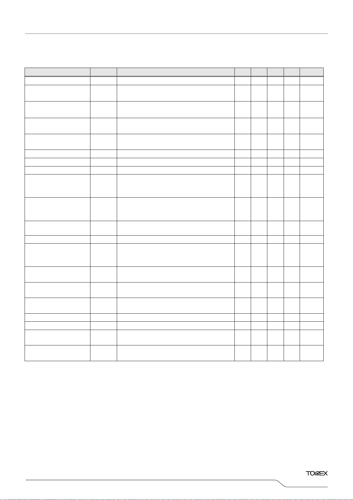
■ELECTRICAL CHARACTERISTICS
XC9515AB04xx
● DC/DC CH1, CH2 (V
PARAMETER SYMBOL CONDITIONS MIN. TYP. MAX. UNITS CIRCUIT
Input Voltage VIN 4.5 5.0 5.5 V
Output Voltage 1 VOUT1
Output Voltage 2 VOUT2
Maximum Output Current 1・2
Current Limit 1・2
Oscillation Frequency f
Maximum Duty Cycle D
Minimum Duty Cycle D
Efficiency 1
Efficiency 2
LX1・2 "H" ON Resistance
LX1・2 "L" ON Resistance
Integral Latch Time 1・2
Soft-Start Time 1・2
EN1・2 "H" Level Voltage
EN1・2 "L" Level Voltage
EN1・2 "H" Level Current
EN1・2 "L" Level Current
LX1・2 "H" Leakage Current
LX1・2 "L" Leakage Current
Test Conditions:
* P_V
DD1・2
**Unless otherwise stated, P_V
*** A_VSS=P_V
NOTE :
*1
:When the difference between the input and the output is small, some cycles may be skipped completely before current maximizes.
If current is further pulled from this state, output voltage will decrease because of P-ch driver ON resistance.
*2:EFFI = { ( output voltage x output current ) / ( input voltage x input current) } x 100
*3
:On resistance (Ω)= (V
*4:Designed value.
*5:Time until it short-circuits LX1 (LX2 in the side of 2CH) with GND via 1Ωof resistor from an operational state and is set to Low level from
current limit pulse generating.
*6:”H” is judged as “H”>VIN-0.1V, ”L” is judged as ”L”<0.1V.
*7
:When temperature is high, a current of approximately 20μA (maximum) may leak.
*8
:Current which EN1 and EN2 are measured separately.
:Lead current which LX1 and LX2 are measured separatel
*9
(*2)
EFFI1
(*2)
EFFI2
stands for P_V
=P_V
SS1
OUT1
=1.5V, V
OUT2
=3.3V, f
OSC
Connected to the external components,
P_V
DD1・2=VEN1=VEN2
Connected to the external components,
P_V
DD1・2=VEN2=VEN1
IOUTMAX1
(*1)
IOUTMAX2
LIM1,
I
I
LIM 2
Connected to the external components, I
OSC
V
MAX
V
MIN
Connected to the external components,
P_V
Connected to the external components,
P_V
LX1H
・RLX2H
R
R
LX1L
・RLX2L
V
OUT1=VOUT2
LX1 and LX2 are pulled down by a resistor of 200Ω
, t
LAT1
t
SS1
LAT2
Time until EN1, EN2 or both pins changes from 0V to
, t
SS2
V
and voltage becomes V
IN
V
V
OUT2
t
VEN1H,
V
EN2H
Voltage which LX1 or LX2 becomes ”H”
VEN1L,
V
EN2L
IEN1H, IEN2H
IEN1L, IEN2L
ILEAK1H,
(*7)
LEAK2H
I
ILEAK1L,
I
LEAK2L
=P_V
DD1
DD2
=5V, V
DD1・2
=0V
SS2
- Lx pin measurement voltage) / 100mA
IN
Voltage which LX1 or LX2 becomes ”L”
P_V
P_V
DD1・2=VLX1=VLX2
P_V
DD1・2
= P_V
EN1=VEN2
=1MHz, EN1・2 Pull-up inside) Ta =25 oC
=0V, I
=0V, I
OUT1=VOUT2
OUT1=VOUT2=VIN
DD1・2=VEN1
=1.5V, I
V
OUT1
DD1・2=VEN2
=3.3V, I
V
OUT2
=0V 100
=5.0V, V
1=200mA
OUT
=5.0V, V
=200mA
OUT2
=0V, ILx1=ILx2=100mA
=Setting Voltage×0.9,
OUT1
= Setting Voltage ×0.9
×0.95, I
OUT1・2
V
OUT1=VOUT2
V
OUT1=VOUT2
P_V
DD1・2=VEN1=VEN2
=5.5V, V
DD1・2
=0V
=0V
EN1=VEN2
=5.5V, V
=5.5V, V
DD1・2
LX1=VLX2=VEN1=VEN2
.
=30mA
OUT1
=30mA
OUT2
=10mA 0.85 1.00 1.15 MHz
OUT
=0V,
EN2
=0V,
EN1
(*3)
(*5)
=10mA
OUT1・2
(*6)
(*6)
=5.5V -
=0V -
=0V - -
EN1=VEN2
=0V
1.470 1.500 1.530 V
3.234 3.300 3.366 V
800
1000
- -
- -
- -
- -
89
-
94
-
0.35
-
0.35
-
6
-
1.3
-
1.2
AVSS
-
-
-6
(*9)
-3.0
- - μA ④
0 %
-
-
(*4)
- Ω ③
(*4)
- Ω -
-
-
V
V
IN
0.4 V
(*8)
0.1
(*8)
- μA ④
(*9)
1.0
mA
mA
%
%
%
ms
ms
μA ④
μA ④
Series
-
①
①
①
②
①
②
②
①
①
⑦
①
④
④
5/21
XC9515 Series
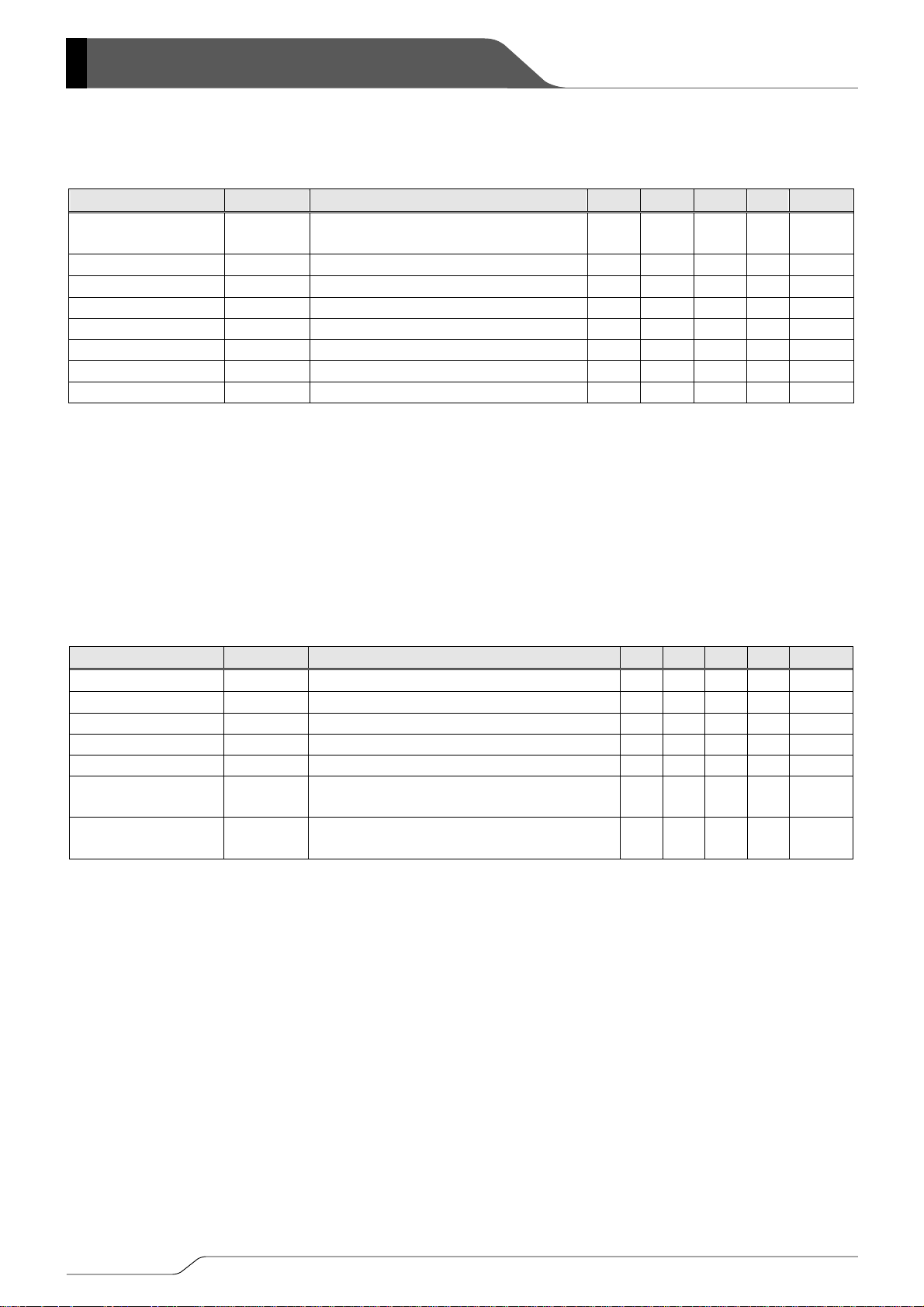
■ELECTRICAL CHARACTERISTICS (Continued)
XC9515AB04xx
●Voltage Detector (VD) (MR pin Pull-up Inside) Block
PARAMETER SYMBOL CONDITIONS MIN. TYP. MAX. UNITS CIRCUIT
Detect Voltage V
Hysteresis Width V
VD Output Current I
Delay Resistance R
MR "H" Level Voltage V
MR "L" Level Voltage V
MR "H" Level Current I
MR "L" Level Current I
Test Conditions:
* P_V
**Unless otherwise stated, P_V
*** A_VSS=P_V
NOTE :
:V
*1
:V
*2
*3
:”H” is judged as “H”>V
stands for P_V
DD1・2
=P_V
SS1
=Detect Voltage
DF(E)
=Release Voltage
DR(E)
(*1)
DF(E)
V
HYS
DOUT
DLY
V
MRH
V
MRL
MRH
MRL
=P_V
DD1
DD2
=5V, V
DD1・2
=0V
SS2
-0.1V, ”L” is judged as “L”<0.1V
IN
P_V
EN1=VEN2
=(V
HYS
DR(E)
DD1・2=VDF
DOUT
DOUT
P_V
P_V
= P_V
(*3)
- V
) / V
DF(E)
-0.01V, Apply 0.5V to V
=”H” Level Voltage
=”L” Level Voltage
DD1・2=VMR
DD1・2
DD1・2
=5.5V - -
=5.5V, VMR=0V -
×100
DF(E)
DOUT
(*3)
1.2 - VIN V
(*3)
AVSS
V
DF(T)
DF(T)
×0.98
V
-
5.0 6.6 8.0 mA
-
-6.0
5.0
2.5
-
V
DF(T)
(*2)
×1.02
-
- MΩ -
0.4 V
0.1
- μA ④
XC9515AB04xx
●Whole Circuit (V
OUT1
=1.5V, V
OUT2
=3.3V, f
=1MHz, EN1・2 Pull-up Inside)
OSC
PARAMETER SYMBOL CONDITIONS MIN. TYP. MAX. UNITS CIRCUIT
Supply Current 1 IDD1 V
Supply Current 2 IDD2
V
OUT1=VOUT2
OUT1=VOUT2
=Setting Voltage x 1.1 (Oscillation stops) -
Stand-by Current ISTB V
UVLO Detect Voltage VUVLOF VIN voltage which V
UVLO Release Voltage VUVLOR VIN voltage which V
Thermal Shutdown
Temperature
Thermal Shutdown
Hysteresis Width
Test Conditions:
* P_V
**Unless otherwise stated, P_V
*** A_VSS=P_V
NOTE :
*1:”H” is judged “H”>V
stands for P_V
DD1・2
SS1
=P_V
TSD
T
HYS
T
=P_V
DD1
=0V
SS2
-0.1V, ”L” is judged “L”<0.1V
IN
DD1・2
DD2
=5V, V
EN1=VEN2
= P_V
=Setting Voltage x 0.9
EN1=VEN2
OUT1
OUT1
DD1・2
=0V
=0V and LX pin becomes ”L”
=0V and LX pin becomes ”H”
950 1500
-
75 145
18 33
-
(*1)
2.4 2.7 3.0 V
(*1)
- -
150
-
20
-
3.5 V
-
-
Ta =2 5oC
V
%
μA ④
⑤
-
④
④
④
Ta =2 5oC
μA ⑥
μA ⑥
μA ⑥
②
②
o
C
o
C
-
-
6/21
■ELECTRICAL CHARACTERISTICS (Continued)
XC9515BA06xx
●DC/DC CH1, CH2 (V
=1.5V, V
OUT1
OUT2
=3.3V, f
=1MHz, EN1 and EN2 pins are internally floating)
OSC
PARAMETER SYMBOL CONDITIONS MIN. TYP. MAX. UNITS CIRCUIT
Input Voltage VIN 2.5
5.5 V
-
Connected to the external components,
Output Voltage1 VOUT1
P_V
DD1・2=VEN1
=30mA
I
OUT1
, V
EN2
=0V
1.470 1.500 1.530 V
Connected to the external components,
Output Voltage2 VOUT2
IOUTMAX1
Maximum Output Current 1・2
Current Limit 1・2
Oscillation Frequency f
Maximum Duty Cycle D
Minimum Duty Cycle D
Efficiency 1
Efficiency 2
LX1・2 "H" ON Resistance
LX1・2 "L" ON Resistance
Integral Latch Time 1・2
Soft-Start Time 1・2
EN1・2 "H" Voltage
EN1・2 "L" Voltage
EN1・2 "H" Current
EN1・2 "L" Current
LX1・2 "H" Leak Current
LX1・2 "L" Leak Current
Test Conditions:
* P_V
**Unless otherwise stated, P_V
*** A_VSS=P_V
NOTE :
*1
:When the difference between the input and the output is small, some cycles may be skipped completely before current maximizes.
*2:EFFI = { ( output voltage x output current ) / ( input voltage x input current) } x 100
*3
:On resistance (Ω)= (V
*4:Designed value.
*5:Time until it short-circuits LX1 (LX2 in the side of 2CH) with GND via 1Ωof resistor from an operational state and is set to Low level
*6:”H” is judged as “H”>VIN-0.1V, ”L” is judged as ”L”<0.1V.
:When temperature is high, a current of approximately 20μA (maximum) may leak.
*7
*8
:Current which EN1 and EN2 are measured separately.
*9
:Lead current which LX1 and LX2 are measured separately.
stands for P_V
DD1・2
If current is further pulled from this state, output voltage will decrease because of P-ch driver ON resistance.
from current limit pulse generating.
(*1)
IOUTMAX2
LIM1, ILIM 2 1000
I
Connected to the external components, I
OSC
V
MAX
V
MIN
(*2)
EFFI1
(*2)
EFFI2
RLX1H, RLX2H V
RLX1L, RLX2L
LAT1, tLAT 2
t
SS1, tSS2
t
EN1H, VEN2H
V
EN1L, VEN2L
V
, I
, I
, I
, I
DD1・2
EN2H
EN2L
leak2H
leak2L
DD2
=5V, V
SS1
=P_V
I
EN1H
I
EN1L
(*7)
I
leak1H
I
leak1L
=P_V
DD1
=0V
SS2
- Lx pin measurement voltage) / 100mA
IN
LX1 and LX2 are pulled down by a resistor of 200Ω
V
= Setting Voltage×0.9, V
OUT1
Time until EN1, EN2 or both pins changes from 0V to V
and voltage becomes V
Voltage which LX1 or LX2 becomes ”H”
Voltage which LX1 or LX2 becomes ”L”
EN1=VEN2
P_V
DD1・2=VEN2
OUT1=VOUT2
OUT1=VOUT2=VIN
Connected to the external components,
P_V
DD1・2=VEN1
=1.5V, I
V
OUT1
Connected to the external components,
P_V
DD1・2=VEN2
=3.3V, I
V
OUT2
OUT1=VOUT2
V
OUT1=VOUT2
V
OUT1=VOUT2
P_V
DD1・2=VEN1=VEN2
P_V
DD1・2
P_V
DD1・2=VLX1=VLX2
P_V
DD1・2
= P_V
=5.5V, V
DD1・2
, V
EN1
=30mA
I
OUT2
=0V 100
=5.0V, V
=200mA
OUT1
=5.0V, V
=200mA
OUT2
=0V, I
=100mA
Lx1=ILx2
= Setting Voltage×0.9
OUT2
×0.95, I
OUT1・2
=0V
=0V
=5.5V - -
=5.5V, V
EN1=VEN2
=5.5V, V
LX1=VLX2=VEN1=VEN2
=0V
=10mA 0.85 1.00 1.15 MHz
OUT
=0V
EN2
=0V
EN1
(*3)
=10mA
OUT1・2
(*6)
(*6)
=0V
=0V - -
EN1=VEN2
=0V
3.234 3.300 3.366 V
800
- -
- -
- -
- -
89
-
94
-
0.35
-
0.35
-
-
(*5)
IN
AVSS
-0.1
-3.0
6
-
1.3
-
1.2
-
(*8)
- - μA ④
(*9)
- - μA ④
0 %
-
-
(*4)
- Ω ③
(*4)
- Ω
-
-
V
V
IN
0.4 V
(*8)
0.1
(*9)
1.0
mA
mA
%
%
%
ms
ms
μA ④
μA ④
XC9515
Series
Ta =2 5 oC
①
①
①
②
①
②
②
①
①
-
⑦
①
④
④
7/21

XC9515 Series
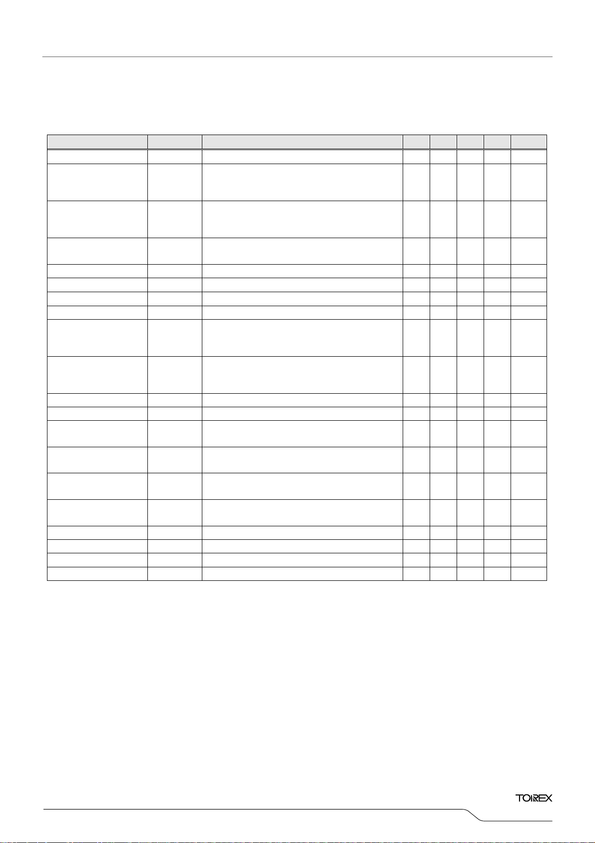
■ELECTRICAL CHARACTERISTICS (Continued)
XC9515BA06xx
●VD (MR pin is) internally floating
PARAMETER SYMBOL CONDITIONS MIN. TYP. MAX. UNITS CIRCUIT
Detect Voltage V
Hysteresis Width VHYS V
VD Output Current IDOUT
Delay Resistance RDLY
MR "H" Level Voltage VMR V
MR "L" Level Voltage VMR V
MR "H" Level Current IMR
MR "L" Level Current IMR
(*1)
2.94 3.00 3.06 V
DF(E)
HYS
P_V
DOUT
DOUT
P_V
P_V
(*2)
={V
-V
}/ V
DR(E)
DD1・2=VDF
DF(E)
-0.01V, Apply 0.5V to V
=”H” Level Voltage
=”L” Level Voltage
=MR=5.5V - -
DD1・2
=5.5V,MR=0V -0.1
DD1・2
×100
DF(E)
DOUT
(*3)
1.2
(*3)
AVSS
5.0 6.6 8.0 mA
5.0
-
2.5
-
-
-
(*8)
- - μA ④
-
- MΩ
VIN V
0.4 V
0.1
Test Conditions:
* P_V
**Unless otherwise stated, P_V
*** A_VSS=P_V
NOTE :
:V
*1
:V
*2
*3
:”H” is judged as “H”>V
stands for P_V
DD1・2
=P_V
SS1
=Detect Voltage
DF(E)
=Release Voltage
DR(E)
=P_V
DD1
=0V
SS2
-0.1V, ”L” is judged as “L”<0.1V
IN
DD1・2
DD2
=5V, V
EN1=VEN2
= P_V
DD1・2
XC9515BA01xx
●Whole Circuit (V
OUT1
=1.5V, V
OUT2
=3.3V, f
=1MHz, EN1 and EN2 pins are internally floating)
OSC
PARAMETER SYMBOL CONDITIONS MIN. TYP. MAX. UNITS CIRCUIT
Supply Current 1 IDD1
Supply Current 2 IDD2
V
OUT1=VOUT2
V
OUT1=VOUT2
= Setting Voltage×0.9 -
= Setting Voltage×1.1 (Oscillation stops) -
Stand-by Current ISTB EN1=EN2=0V
UVLO Detect Voltage VUVLOF VIN voltage which V
UVLO Release Voltage VUVLOR VIN voltage which V
Thermal Shutdown
Temperature
Thermal Shutdown
Hysteresis Width
T
TSD
HYS
T
=0V and LX pin becomes ”L”
OUT1
=0V and LX pin becomes ”H”
OUT1
(*1)
(*1)
950 1500
75 145
5.5 11
-
1.5 1.8 2.1 V
150
20
2.3 V
-
-
- -
-
-
Test Conditions:
* P_V
**Unless otherwise stated, P_V
*** A_VSS=P_V
NOTE :
*1:”H” is judged “H”>V
stands for P_V
DD1・2
SS1
=P_V
DD1
=P_V
=0V
SS2
-0.1V, ”L” is judged “L”<0.1V
IN
DD1・2
DD2
=5V, V
EN1=VEN2
= P_V
DD1・2
8/21
Ta =2 5 oC
⑤
% -
④
-
④
④
μA ④
Ta =2 5 oC
μA ⑥
μA ⑥
μA ⑥
②
②
o
C -
o
C -

■TYPICAL APPLICATION CIRCUIT
VIN
CIN1 CL1
PVDD
NC
PVSS
1
NC
PVSS
2
NC
PVDD2NC
CIN2
<Example of the External Components>
L1 :4.7μH(CDRH4D28C, SUMIDA)
L2 :4.7μH(CDRH4D28C, SUMIDA)
:10μF(ceramic)
C
IN1
:10μF(ceramic)
C
IN2
:10μF(ceramic)
C
L1
:10μF(ceramic)
C
L2
RUP :100kΩ
XC9515
Series
L1
1
NC
LX1
EN1
EN2
VOUT
1
MR
AVSS
Cd
VOUT
2
LX2
NC
VDOUT
RUP
L2
VOUT1
EN1
EN2
MR
Cd
CL2
VDOUT
VOUT2
9/21

DD1
and P_V
Limit < # ms
pin through split resistors, R
OUT
and R
FB1
voltages drop below the low level of EN1 and EN2 pin.)The latch operation
DD2
. When a voltage lower than the reference is fed back, the output
FB2
Limit < # ms
and R
FB1
. Phase
FB2
XC9515 Series
■OPERATIONAL EXPLANATION
XC9515 series consists of a reference voltage source, ramp wave circuit, error amplifier, PWM comparator, phase
compensation circuit, output voltage adjustment resistors, P-channel driver transistor, N-channel synchronous switching
transistor, current limit circuit, UVLO circuit and others. The series ICs compare, using the error amplifier, the voltage of the
internal voltage reference source with the feedback voltage from V
compensation is performed on the resulting error amplifier output, to input a signal to the PWM comparator to determine the
turn-on time during PWM operation. The PWM comparator compares, in terms of voltage level, the signal from the error
amplifier with the ramp wave from the ramp wave circuit, and delivers the resulting output to the buffer driver circuit to cause
the Lx pin to output a switching duty cycle. This process is continuously performed to ensure stable output voltage. The
current feedback circuit monitors the P-channel driver transistor current for each switching operation, and modulates the error
amplifier output signal to provide multiple feedback signals. This enables a stable feedback loop even when a low ESR
capacitor, such as a ceramic capacitor, is used, ensuring stable output voltage.
<Reference Voltage Source>
The reference voltage source provides the reference voltage to ensure stable output voltage of the DC/DC converter.
<Ramp Wave Circuit>
The ramp wave circuit determines switching frequency. The frequency is fixed internally at 1MHz. Clock pulses generated
in this circuit are used to produce ramp waveforms needed for PWM operation, and to synchronize all the internal circuits.
<Error Amplifier>
The error amplifier is designed to monitor output voltage. The amplifier compares the reference voltage with the feedback
voltage divided by the internal split resistor, R
voltage of the error amplifier increases. The gain and frequency characteristics of the error amplifier output are fixed
internally to deliver an optimized signal to the mixer.
<Current Limit>
The current limiter circuit of the XC9515 series monitors the current flowing through the P-channel MOS driver transistor
connected to the Lx pin, and features a combination of the current limit mode and the latch mode.
①When the driver current is greater than a specific level (peak value of coil current), the current limit function operates to off
the pulses from the Lx pin at any giving timing.
②When the driver transistor is turned off, the limiter circuit is then released from the current limit detection state.
③At the next pulse, the driver transistor is turned on. However, the transistor is immediately turned off in the case of an
over current state.
④When the over current is eliminated, the IC resumes its normal operation.
The IC waits for the over current state to end by repeating the steps ① to ③. If an over current state continues for a few
ms and the above three steps are repeatedly performed, the IC performs the function of latching the OFF state of the
driver transistor. Both two DC/DC blocks stop operations when either CH1 or CH2 of protection circuit is activated. At
this time, both Lx1 and Lx2 become high impedance. Once the IC is in latch mode, operations can be resumed by either
turning the IC off after letting EN1 and EN2 pins down to low level, or by restoring power. For restoring power, the IC
should be turned off after P_V
can be released from the current limit detection state because of the circuit’s noise. Also, depending on the state of the
PC Board, latch time may become longer and latch operation may not work. In order to avoid the effect of noise, the
board should be laid out so that capacitors are placed as close to the chip as possible.
10/21
XC9515
■OPERATIONAL EXPLANATION (Continued)
<Thermal Shutdown>
For protecting the IC from heat damage, the thermal shutdown circuit monitors the chip temperature. When the chip
temperature reaches 150℃, the thermal shutdown circuit operates and the driver transistor will be set to OFF. As the chip
temperature drops to 130℃ by stopping current flow, the soft-start function operates to turn the output on.
<Short-Circuit Protection>
The short-circuit protection circuit monitors the FB voltage. If the output is shorted incorrectly with the ground, the
short-circuit protection circuit operates and turns the driver transistor off to latch when the FB voltage becomes less than half
of the setting voltage. Both two DC/DC blocks stop operations when either CH1 or CH2 of protection circuit is activated. At
this time, both Lx1 and Lx2 become high impedance. Once the IC is in latch mode, operations can be resumed by either
turning the IC off after letting both ends of EN1 and EN2 pins down to low level, or by restoring power. (The P_V
voltages should be less than the low level of the EN1 and EN2 pins when restoring power.)
P_V
DD2
<Soft Start Function>
The soft-start circuit protects against inrush current, when the power is switched on, and also to protect against voltage
overshoot. It should be noted, however, that this circuit does not protect the load capacitor (C
L) from inrush current. With
the Vref voltage limited and depending upon the input to the error amps, the operation maintains a balance between the two
inputs of the error amps and controls the EXT1 pin's ON time so that it doesn't increase more than is necessary.
<UVLO Circuit>
When the V
forced OFF to prevent false pulse output caused by unstable operation of the internal circuitry. When the V
IN pin voltage becomes1.8V (TYP.) or lower (for XC9515A, 2.7V or lower), the P-channel output driver transistor is
IN pin voltage
becomes 1.9V (TYP.) or higher (for XC9515A, 3.0V or lower), switching operation takes place. By releasing the UVLO
function, the IC performs the soft-start function to initiate output startup operation.
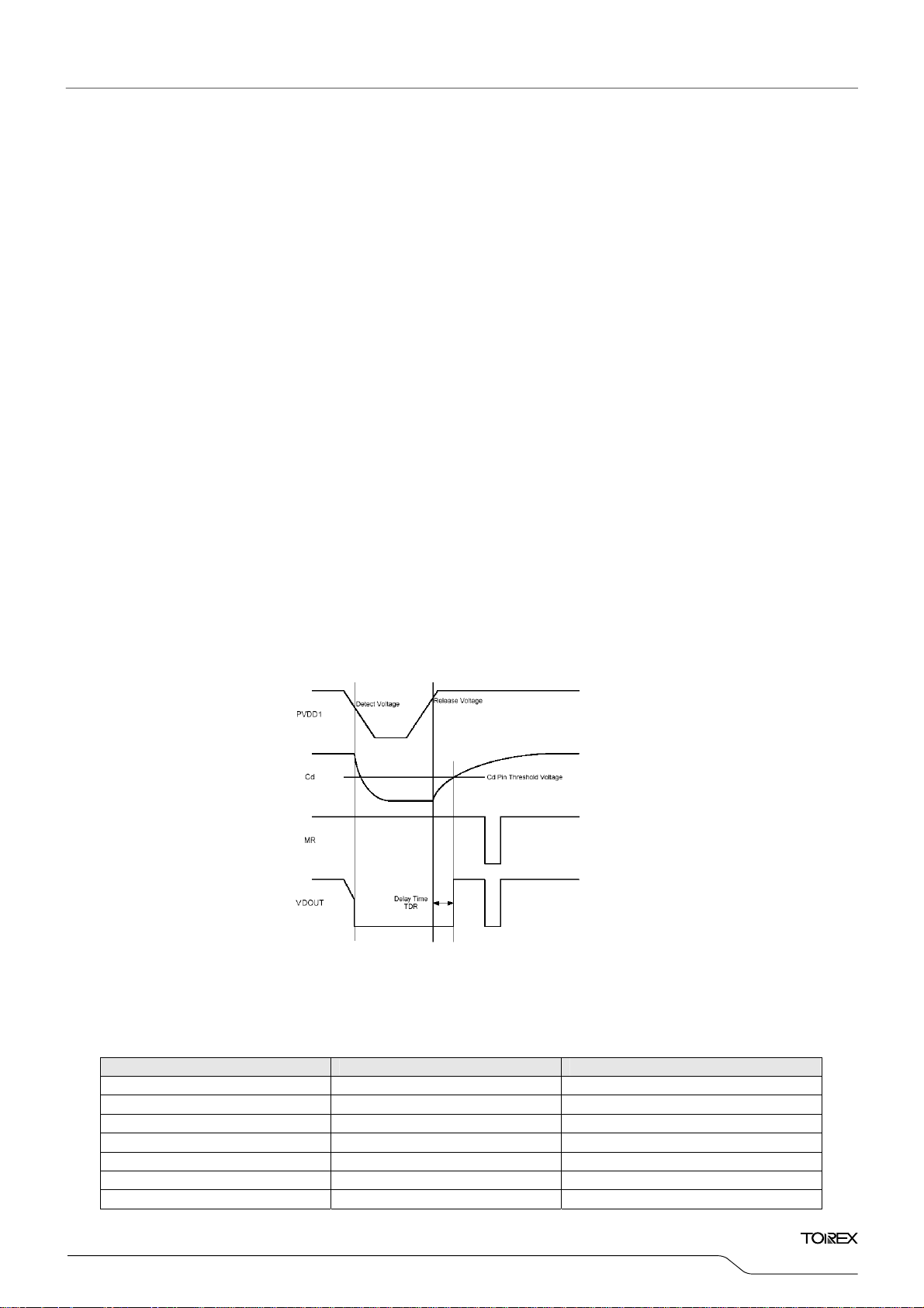
<Voltage Detector Block>
The series' detector function monitors the voltage divided by resistors connected to the P_V
DD1 pin, as well as monitoring the
voltage of the internal reference voltage source via the comparator. Because of hysteresis at the detector function, output at
the V
of the detect voltage). The output configuration of the V
required. The voltage detector block has a manual reset (MR) pin. By setting the MR pin at low level, the V
pin will invert when the sense pin voltage of the detector block (P_VDD1) increases above the release voltage (105%
DOUT
pin is N-channel open drain, therefore, a pull-up resistor is
DOUT
pin is forced
DOUT
to be at low level.
By connecting a capacitor (Cd) to the Cd pin, the XC9515 series can set a delay time to VDOUT pin’s output signal when
releasing voltage. The delay time can be calculated from the internal resistance, Rdelay (2.5MΩ fixed TYP.) and the
value of Cd as per the following equation. As selecting the capacitor (Cd), the delay time can be set freely.
t
(Delay time) =Cd x Rdelay x 0.69
DR
●Release Delay Ta=25oC
Delay Capacity Cd [μF] Release Delay tDR (TYP.) [ms] Release Delay tDR (MIN.~MAX.) [ms]
0.01 17 10~24
0.022 38 23~53
0.047 81 49~113
0.1 173 103~242
0.22 380 228~532
0.47 811 487~11 35
1 1725 1035~2415
Series
and
DD1
11/21

XC9515 Series
■NOTES ON USE
1. Please use this IC within the stated maximum ratings. The IC is liable to malfunction should the ratings be exceeded.
2. Please apply the same electrical potential to the P_V
P_V
and P_V
3. The XC9515 series is designed for use with ceramic output capacitors. If, however, the potential difference between
4. When the peak current, which exceeds limit current flows within the specified time, the built-in driver transistor is turned off
5. When the input voltage is low, limit current may not be reached because of voltage falls caused by ON resistance or serial
6. Since the potential difference for input voltage has occurred to the both ends of a coil, the time changing rate of the coil
DD1
causes malfunction. Also the same electrical potential should be applied to the P_V
dropout voltage or output current is too large, a ceramic capacitor may fail to absorb the resulting high switching energy and
the output could be unstable. If the input-output potential difference is large, use a larger output capacitor to compensate for
insufficient capacitance.
(the integral latch circuit). During the time until it detects limit current and before the built-in transistor can be turned off, the
current for limit current flows; therefore, care must be taken when selecting the rating for the coil.
resistance of the coil.
current is large when the P-channel driver transistor is ON. On the other hand, since the V
when the N-channel transistor is ON and there is almost no potential difference of the coil both ends, the time changing rate
of the coil current becomes very small.
This operation is repeated and the delay time of the circuit also influences, therefore, the coil current is converged on the
current value beyond the amount of current which should be restricted essentially.
The short-circuit protection does not operate during the soft-start time. As soon as the soft-start time finishes, the
short-circuit protection starts to operate and the circuit becomes disable.
The delay time of the circuit also influences when step-down ratio is large, as the result, a current more than over current
limit may flow. Please do not exceed the absolute maximum ratings of the coil.
① A current flows to the driver transistor up to the current limit (I
② For the delay time of the circuit, a current more than the I
transistor turns off.
③ Time changing rate of the coil current becomes very small because there is no potential difference between both ends
of the coil.
④ The Lx pin oscillates a narrow pulse during the soft-start time because of the current limit.
⑤ The circuit is latched since the short-circuit protection operates and the P-channel driver transistor is turned off.
pins should have the same electrical potential. Applying the electrical potential to only one side
DD2
and P_V
DD1
pins. Even where either CH1 or CH2 is used, both
DD2
).
LIM
flows after the I
LIM
# ms
, P_V
SS1
decide until the P channel driver
LIM
and A_VSS pins.
SS2
pin short-circuits to the GND
OUT
12/21

XC9515
Series
■NOTES ON USE (Continued)
7. Driving current below the minimum operating voltage may lead malfunction to the UVLO circuit because of the noise.
8. Depending on the PC board condition, the latch function may be released from limit current detection state and the latch
time may extend or fail to reach the latch operation. Please locate the input capacitance as close to the IC as possible.
9. Spike noise and ripple voltage arise in a switching regulator as with a DC/DC converter. These are greatly influenced by
external component selection, such as the coil inductance, capacitance values, and board layout of external components.
Once the design has been completed, verification with actual components should be done.
10. With the DC/DC converter block of the IC, the peak current of the coil is controlled by the current limit circuit. Since the
peak current increases when dropout voltage or load current is high, current limit starts operating, and this can lead to
instability. When peak current becomes high, please adjust the coil inductance value and fully check the circuit operation.
In addition, please calculate the peak current according to the following formula:
Peak current: Ipk = (V
L: Coil Inductance Value, f
IN - V
) x OnDuty / (2 x L x fosc) + I
OUT
: Oscillation Frequency
OSC
OUT
11. When the load current is light in PWM control, very narrow pulses will be outputted, and there is the possibility that some
cycles may be skipped completely.
12. When the difference between V
IN and VOUT is small, and the load current is heavy, very wide pulses will be outputted and
there is the possibility that some cycles may be skipped completely.
13. If the power input pin voltage is assumed to decrease rapidly (ex. from 6.0V to 0V) at the release of the operation
although delay capacitance (Cd) pin is connected, please connect an Shottky barrier diode between the power input
(P_V
) pin and the delay capacitance (Cd) pin.
DD1
14. Please connect a pull-up resistor with 100 to 200kΩ to the output pin of the voltage detector block (V
DOUT
).
15. The delay time of the voltage detector block in heavy load may extend because of the noise of the DC/DC block.
Precipitous and large voltage fluctuation at the power input pin may cause malfunction of the IC.
16. Use of the IC at voltages below the minimum operating voltage may lead the output voltage drop before achieving over
current limit.
17. When P_VDD1 and P_VDD2 power supply pins and EN1 and EN2 enable pins are in undefined states, the latch
protection circuit may not be reset so that the IC operation does not start correctly. Power supply and enable pins
(EN1,EN2) should be grounded before starting the IC operation.
【Undefined state conditions for each pin】
P_V
=P_VDD2=0.1V ~ 1.2V
DD1
V
EN1=VNE2
= 0.4V ~ 1.2V
18. UVLO function works even if when V
input voltage falls below the UVLO voltage in very short time period like a few ten
IN
nanoseconds.
●Instruction on Pattern Layout
1. In order to stabilize VIN's voltage level, we recommend that a by-pass capacitor (CIN1 and CIN2) be connected as close
as possible to the P_V
2. Please mount each external component as close to the IC as possible.
3. Wire external components as close to the IC as possible and use thick, short connecting traces to reduce the circuit
impedance.
4. Make sure that the V
at the time of switching may result in instability of the DC/DC converter.
・P_V
DD1
traces are as thick as possible, as variations in the VSS potential caused by high VSS currents
SS
pins and P_V
DD2
SS1
・P_V
SS2
pins.
13/21

XC9515 Series
■TEST CIRCUITS
< Test Circuit No.1 >
CL
CL
Wave Form Measurement Point
Wave Form Measurement Point
L
CIN
CIN
L
Wave Form Measurement Point
Wave Form Measurement Point
LX1
PVDD1
PVSS1
PVSS2
PVDD2 CD
LX2 VDOUT
EN1
EN2
VOUT1
MR
AVSS
VOUT2
A
V
※ External Components
L : 4.7μH(CDRH4D28C : SUMIDA)
CIN : 10μF (ceramic)
CL : 10μF (ceramic)
A
V
< Test Circuit No.2 >
A
1μF
V
< Test Circuit No.3 >
1μF
Wave Form Measurement Point
Wave Form Measurement Poi nt
A
V
A
m100 A
A
V
V
m100 A
A
LX1
PVDD1
PVSS1
PVSS2
PVDD2 CD
LX2 VDOUT
V
Wave Form Measurement Point
Wave Form Measurement Poi nt
LX1
PVDD1
PVSS1
PVSS2
PVDD2 CD
LX2 VDOUT
EN1
EN2
VOUT1
MR
AVSS
VOUT2
EN1
EN2
VOUT1
MR
AVSS
VOUT2
14/21
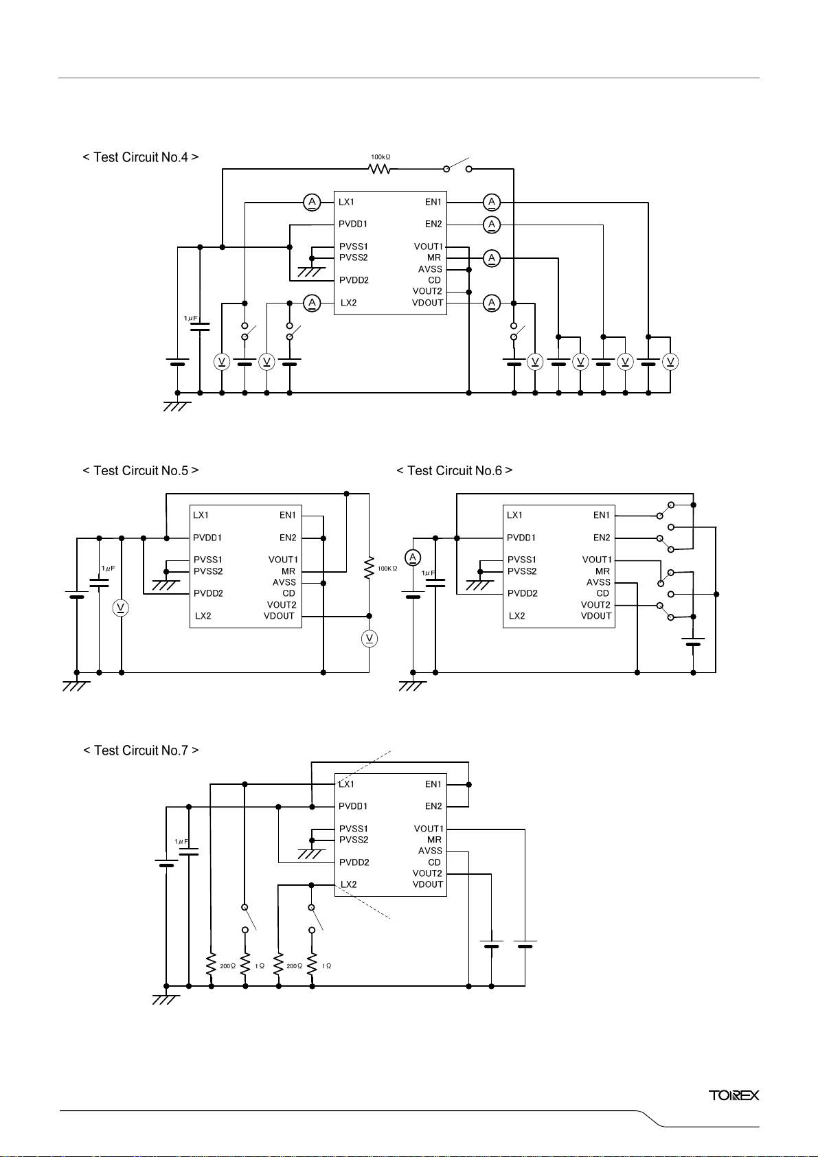
■TEST CIRCUITS (Continued)
XC9515
Series
Wave Form Measurement Point
Wave Form Measurement Point
15/21

XC9515 Series
■TYPICAL PERFORMANCE CHARACTERISTICS
(1) Efficiency vs. Output Current
100
90
80
70
60
50
40
Efficiency[%]
30
Efficiency: EFFI (%)
20
10
(2) Output Voltage vs. Output Current
Output Voltage: VOUT (V)
Output Vo ltage : VOUT[V]
(V)
OUT
Output Voltage: V
Output V olta ge : V OUT[V ]
VOUT=3.3V
0
1 10 100 1000
1.60
1.55
1.50
1.45
1.40
1 10 100 1000
3.40
3.35
3.30
3.25
3.20
1 10 100 1000
L=4.7uH(CDRH4D28C),CIN=10uF(c eramic ),C L=10uF( cerami c)
VOUT=1.8V
Output Current: I
Output Current : IOUT [mA]
VOUT=1.5V VOUT=1.8V
L:4.7 uH(CDRH4 D28C),CIN= 10uF(ce ra mic) ,CL=10uF(ce ramic)
Output Current : IOUT[m A]
Output Current: I
VOUT= 3.3V
L:4.7 uH(CDRH4 D28C),CIN= 10uF(ce ra mic) ,CL=10uF(ce ramic)
Output Current : IOUT[m A]
Output Current: I
OUT
OUT
(mA)
(mA)
OUT
(mA)
VIN=5V,FOSC=1MHz
VOUT=1.5V
VIN=5.0V
1.90
1.85
1.80
1.75
Output V oltage : VOUT[V]
1.70
1 10 100 1000
VIN=5.0V
L:4.7uH(CDRH4D28C),CIN=10uF(ceramic), CL=10uF(ceramic)
Output Current : IOUT[mA]
Output Current: I
OUT
(mA)
VIN=5.0V
16/21
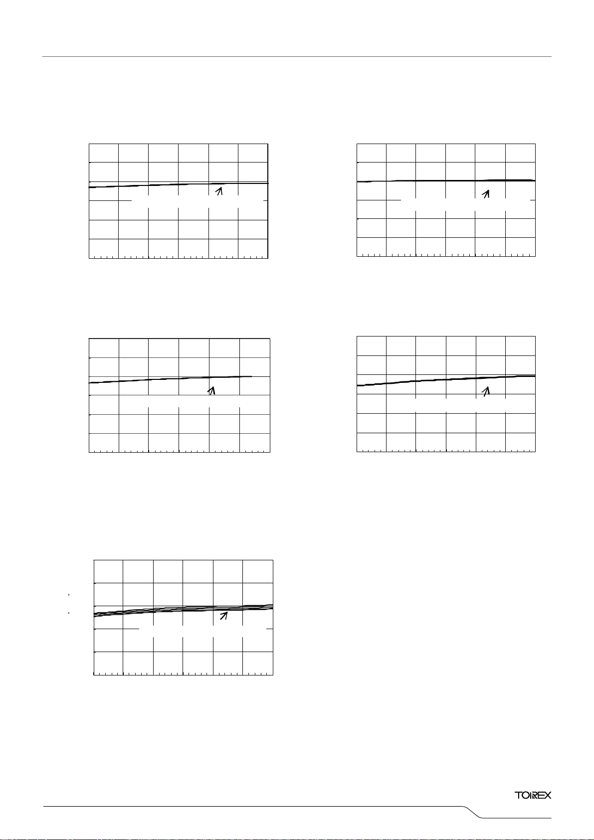
■TYPICAL PERFORMANCE CHARACTERISTICS (Continued)
(3) Output Voltage vs. Ambient Temperature
V
1.30
=1.2V V
OUT
Vout =1.2V Vout= 1.5V
L:4.7uH( CDRH4D28C ),C IN=10uF(c eram ic),CL=10uF(ce ramic)
VIN=2.5V,3. 0V,4. 0V,5.0V, 5.5V
1.60
=1.5V
OUT
L:4.7 uH(CDRH 4D28C),CIN =10uF(ceramic) ,CL=10uF(ceramic)
1.25
1.20
1.55
1.50
1.15
1.10
VIN=2.5V,3.0V,4. 0V,5. 0V,5.5 V
1.45
1.40
VIN=2 .5V,3.0V,4.0V,5.0V,5. 5V
1.05
Output V olta ge:Vo ut1[v]
1.00
-50 -25 0 25 50 75 100
Ambi ent Tem perature:T a[℃ ]
1.35
Outpu t Voltage: Vou t1[v]
1.30
-50-25 0 255075100
Ambient T emp erature: Ta[℃ ]
1.90
1.85
1.80
1.75
Voltage: Vout1 [v]
1.70
1.65
Output
1.60
-50-250 255075100
V
=1.8V V
OUT
Vout=1.8V Vout=3.3V
L:4.7uH( CDRH4D28C ),C IN=10uF(c eram ic),CL=10uF(ce ramic)
VIN=2.5V,3.0V,4.0V,5.0V ,5.5V
Ambi ent Tempe rature:Ta[℃ ]
VIN=2.5V,3. 0V,4. 0V,5.0V, 5.5V
L:4.7uH(CDRH 4D28C),CIN =10uF (ceramic) ,CL =10uF(ceramic)
3.40
3.35
3.30
3.25
3.20
3.15
Output V olta ge:Vou t2[v ]
3.10
-50 -25 0 25 50 75 100
Ambient Temperature:Ta[℃ ]
=3.3V
OUT
VIN=4.0V,5 .0V,5.5V
(4) Oscillation Frequency vs. Ambient Temperature
f
=1MHz
1.2
(MHz)
OSC
1.1
OSC
FOSC=1MHz
L:4.7uH(CDRH4D28C),CIN=10uF(ceramic),CL=10uF(ceramic)
VIN=2.5V,3.0V,4.0V,5.0V,5.5V
1.0
0.9
:FOSC[MHz]
0.8
Oscillation Frequency
Oscillation Frequency: f
0.7
-50 -25 0 25 50 75 100
VIN=2.5V,3.0V,4.0V, 5.0V,5.5V
Ambient Temperature:Ta[℃ ]
XC9515
Series
VIN=2.5V, 3.0V,4.0V,5.0 V,5.5V
VIN =4.0V,5.0 V,5.5V
17/21
OSC
=1MHz
=1MHz
OSC
=1MHz
OSC
VOUT1= 200mV/div
VOUT2= 200mV/div
IOUT1=200mA
IOUT1=1mA
VOUT1= 200mV/div
VOUT2= 200mV/div
IOUT1=800mA
IOUT1=200m A
VOUT1= 200mV/div
VOUT2= 200mV/div
XC9515 Series
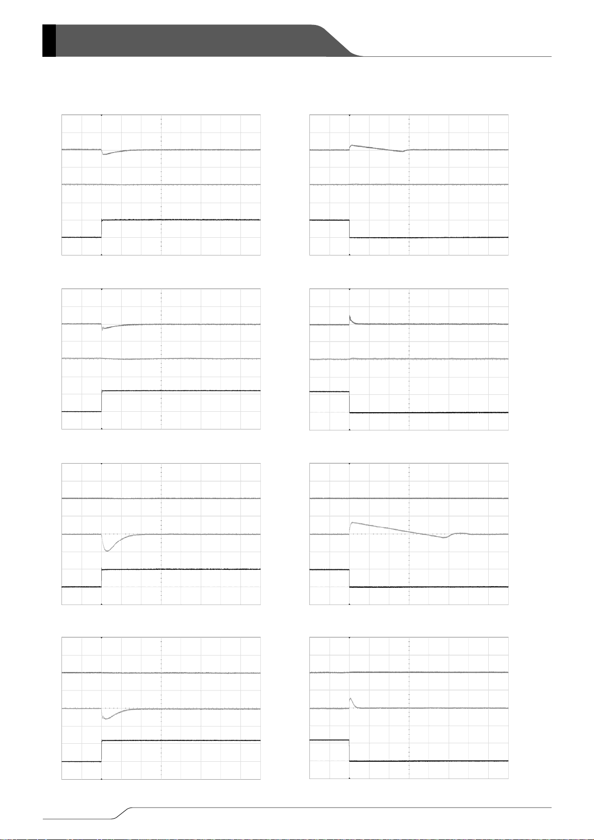
■TYPICAL PERFORMANCE CHARACTERISTICS (Continued)
(5) Load Transient Response
V
=5V, V
IN
VIN=5V,VOUT1=1.5V,VOUT2=3.3V,FOSC=1MHz,
VOUT1=20 0mV/div
VOUT2=20 0mV/div
IOUT1=1mA
VIN=5V, V
VIN=5V,VOUT1=1.5V,VOUT2=3.3V,FOSC=1MHz,
VOUT1=20 0mV/div
VOUT2=20 0mV/div
IOUT1=200mA
VIN=5V, V
VIN=5V,VOUT1=1.5V,VOUT2=3.3V,FOSC=1MHz,
VOUT1=20 0mV/div
VOUT2=20 0mV/div
=1.5V, V
OUT1
IOUT1=200mA
=1.5V, V
OUT1
IOUT1=800mA
OUT1
=3.3V, f
OUT2
50μs/div 200μs/div
50μs/div 200μs/div
=3.3V, f
OUT2
50μs/div 200μs/div
50μs/div 200μs/div
=1.5V, V
OUT2
=3.3V, f
IOUT2=200mA
IOUT2=1mA
50μs/div 200μs/div
50μs/div 200μs/div
VIN=5V, V
VIN=5V,VOUT1=1.5V,VOUT2=3.3V,FOSC=1MHz,
VOUT1=20 0mV/div
VOUT2=20 0mV/div
IOUT2=200mA
=1.5V, V
OUT1
IOUT2=800mA
50μs/div 200μs/div
50μs/div 200μs/div
OUT2
=3.3V, f
OSC
18/21
IOUT2=200mA
IOUT2=1mA
=1MHz
VOUT1= 200mV/div
VOUT2= 200mV/div
IOUT2=800mA
IOUT2=200m A

■PACKAGING INFORMATION
●QFN-20 Unit: mm
1 PIN INDENT
4.00±0.10
2.70±0.05
4.00±0.10
0.40±0.05
106789
(0.2)
+0.03
0.02
-0.02
0.75±0.05
XC9515
Series
0.20±0.05
5
4
3
2
2.70±0.05
1
11
12
13
14
15
*The solder filet may not be formed because of no plating at side.
(0.5)
20
19
161718
●QFN-20 Reference Pattern Layout ●QFN-20 Reference Metal Mask Design
4.6
3.2
0.3
3.2
4.6
2.7
4.5
3.3
4.5
3.3
0.3 1.1
0.5
2.7
0.3
Thickness of solder paste:120μm (reference)
0.5
1.10.3
19/21

XC9515 Series
■MARKING RULE
●QFN-20
1pin
①②③④⑤⑥
⑦⑧⑨
20/21
QFN-20
(TOP VIEW)
●Standard Product
①②③ represent product series
MARK
① ② ③
PRODUCT SERIES
5 1 5 XC9515******-G
④Input Voltage Range, UVLO Voltage
MARK PRODUCT SERIES OPTIONAL FUNCTIONS
A XC9515A*****-G
B XC9515B*****-G
⑤EN Pin, MR Pin, Internal Control
MARK
PRODUCT SERIES OPTIONAL FUNCTIONS
A XC9515*A****-G
B XC9515*B****-G
C XC9515*C****-G
D XC9515*D****-G
⑥⑦ represents integer number of setting voltage
MARK
⑥ ⑦
0 1 XC9515**01**-G
⑧⑨ represents production lot number
Order of 01, …09, 10, 11, …99, 0A, …0Z, 1A, …9Z, A0, …Z9, AA, …ZZ.
(G, I, J, O, Q, W excluded)
*No character inversion used.
Input Voltage Range 5V±10%, UVLO
Voltage 2.7V (TYP.)
Input Voltage Range 2.5V~5.5V, UVLO
Voltage 1.8V (TYP.)
EN1, EN2 Pin Open
MR Pin Open
Built-in EN1, EN2 Pin Pull-up Resistance
Built-in MR Pin Pull-up Resistance
EN1, EN2 Pin Open
Built-in MR Pin Pull-up Resistance
Built-in EN1, EN2 Pin Pull-up Resistance
MR Pin Open
PRODUCT SERIES

XC9515
Series
1. The products and product specifications contained herein are subject to change without
notice to improve performance characteristics. Consult us, or our representatives
before use, to confirm that the information in this datasheet is up to date.
2. We assume no responsibility for any infringement of patents, patent rights, or other
rights arising from the use of any information and circuitry in this datasheet.
3. Please ensure suitable shipping controls (including fail-safe designs and aging
protection) are in force for equipment employing products listed in this datasheet.
4. The products in this datasheet are not developed, designed, or approved for use with
such equipment whose failure of malfunction can be reasonably expected to directly
endanger the life of, or cause significant injury to, the user.
(e.g. Atomic energy; aerospace; transport; combustion and associated safety
equipment thereof.)
5. Please use the products listed in this datasheet within the specified ranges.
Should you wish to use the products under conditions exceeding the specifications,
please consult us or our representatives.
6. We assume no responsibility for damage or loss due to abnormal use.
7. All rights reserved. No part of this datasheet may be copied or reproduced without the
prior permission of TOREX SEMICONDUCTOR LTD.
21/21
 Loading...