

■
■
A
■
■
X
p
XC9509 Series
ETR1006_001
Synchronous Step-Down DC/DC Converter
with Built-In LDO Regulator in Parallel Plus Voltage Detector
GENERAL DESCRIPTION
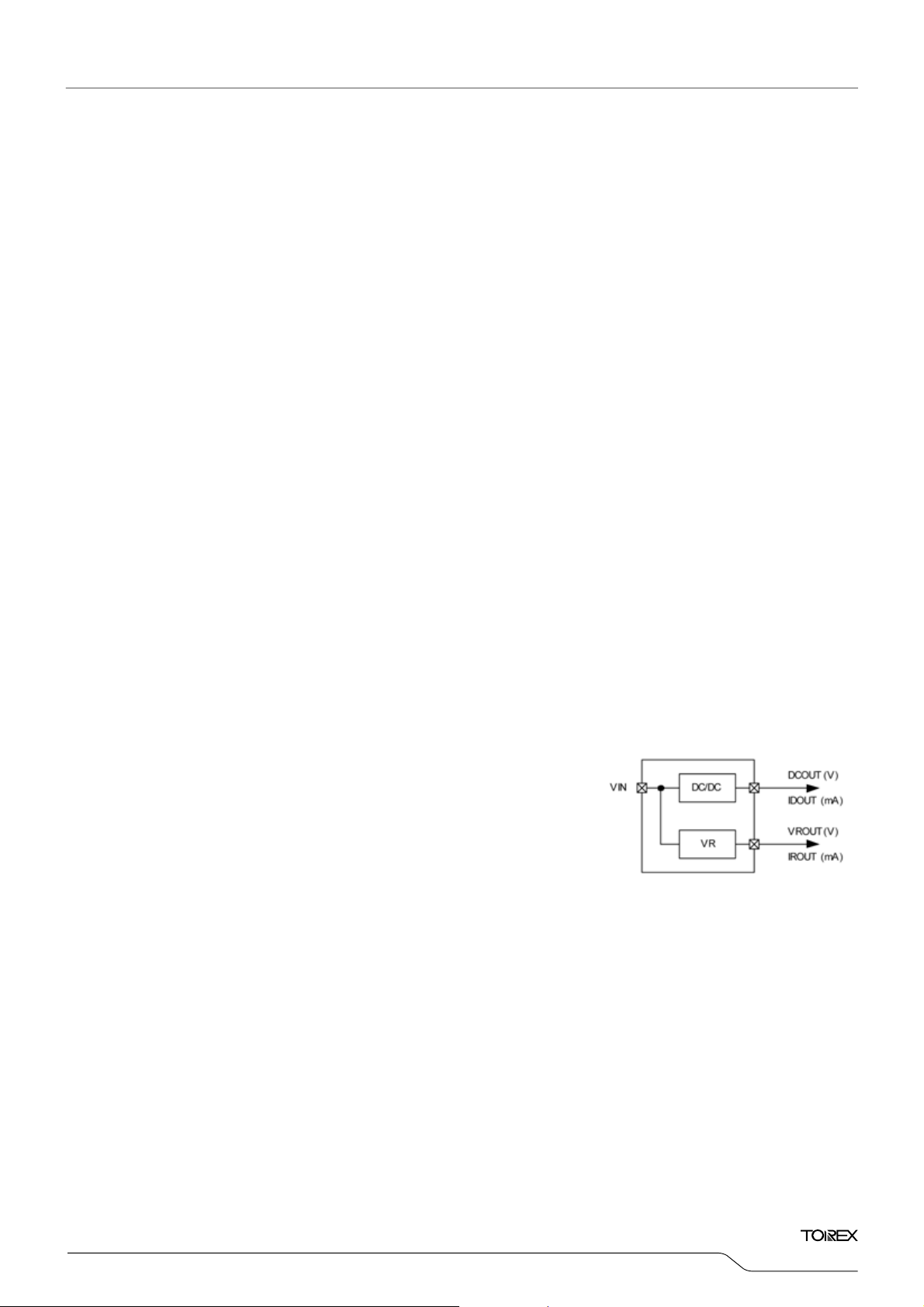
The XC9509 series consists of a step-down DC/DC converter and a high-speed LDO regulator connected in parallel with the
DC/DC converter's output. A voltage detector is also built-in. Since the input for the LDO voltage regulator block comes
from the input power supply, it is suited for use with various applications.
The DC/DC converter block incorporates a P-channel driver transistor and a synchronous N-channel switching transistor.
With an external coil, diode and two capacitors, the XC9509 can deliver output currents up to 600mA at efficiencies over 90%.
The XC9509 is designed for use with small ceramic capacitors.
A choice of three switching frequencies are available, 300kHz, 600kHz, and 1.2MHz. Output voltage settings for the DC/DC
and VR are set-up internally in 100mV steps within the range of 0.9V to 4.0V (± 2.0%). For the VD, the range is of 0.9V to
5.0V (± 2.0%). The soft start time of the series is internally set to 5ms. With the built-in U.V.L.O. (Under Voltage Lock Out)
function, the internal P-channel driver transistor is forced OFF when input voltage becomes 1.4 V or lower. The functions of
the MODE pin can be selected via the external control pin to switch the DC/DC control mode and the disable pin to shut down
either the DC/DC block or the regulator block.
PPLICATIONS
●CD-R / RW, DVD
●HDD
●PDAs, portable communication modem
●Cellular phones
●Palmtop computers
●Cameras, video recorders
TYPICAL APPLICATION CIRCUIT
MSOP-10 (TOP VIEW)
* Please refer to the typical application circuit when
external com
onents are selected.
FEATURES
Input Voltage Range : 2.4V ~ 6.0V
Low ESR Capacitor : Ceramic capacitor compatible
VD Function : Sense internally either V
or V
Small Package : MSOP-10, USP-10
<DC/DC Converter Block>
Output Voltage Range : 0.9V ~ 4.0V (Accuracy±2%)
Output Current : 600mA (for MSOP-10 package)
400mA (for USP-10 package)
Control Method : PWM or PWM/PFM Selectable
Oscillation Frequency : 300kHz, 600kHz, 1.2MHz
<Regulator Block>
Reglator Output : Parallel Input to DC/DC Converter
Output Voltage Range : 0.9V ~ 4.0V (Accuracy±2%)
Current Limit : 300mA
Dropout Voltage : 80mV @ I
High Ripple Rejection : 60dB @1kHz (V
ROUT. N-ch open drain output
OUT=100mA (VOUT=2.8V)
OUT=2.8V)
DD, DCOUT,
■TYPICAL PERFORMANCE
CHARACTERISTICS
C9509Hxxxx
CIN:4.7μF (ceramic), CL1:10μF (ceramic), CL2: 4.7μF (ceramic)
VIN=3.6V, Topr=25℃, L=4.7μH (CDRH4D28C),
1/41
■
■
■
XC9509 Series
PIN CONFIGURATION
●Control Methods, MODE Pins, VD SENSE Pins
* The XC9509A to F series' MODE pin switches either the regulator block or DC/DC block to stand-by mode.
*The dissipation pad for the USP-10 package
should be solder-plated in recommended
mount pattern and metal masking so as to
enhance mounting strength and heat release.
If the pad needs to be connected to other pins,
it should be connected to the AGND pin.
PRODUCT CLASSIFICATION
●Ordering Information
XC9509①②③④⑤⑥ : The input for the voltage regulator block comes from VDD.
DESIGNATOR DESCRIPTION SYMBOL DESCRIPTION
①
②③
④
⑤
⑥
SERIES ① DC/DC CONTROL METHODS
XC9509
When the CE mode is off, every function except for the VD function enters into the stand-by mode.
(The MODE pin does not operate independently.)
MSOP-10 (TOP VIEW)
USP-10 (BOTTOM VIEW)
Control Methods, the
MODE Pin, & the VD
Sense Pin
Setting Voltage &
Specifications
DC/DC Oscillation
Frequency
Package &
DC/DC Current Limit
Device Orientation
A VDD
B DCOUT
C
D VDD
E DCOUT
F
H VDD
K DCOUT
L
PWM Control
PWM, PFM/PWM Manual
Switch
As chart below : -
Internal
standard
3 : 300kHz
6 : 600kHz
C : 1.2MHz
A : MSOP-10, Current limiter: 1.1A (TYP.)
D : USP-10, Current limiter: 0.7A (TYP.)
R : Embossed Tape, standard feed
L : Embossed Tape, reverse feed
PIN ASSIGNMENT
PIN NUMBER PIN NAME FUNCTION
1 PGND Power Ground
2 CE Chip Enable
3 PVDD Power Supply 1
4 AVDD Power Supply 2
5 VDOUT VD Input
6 AGND Analog Ground
7 MODE Mode Switch
8 VROUT VR Output
9 DCOUT DC/DC Output Sense
10 LX Switch
: Setting voltage and specifications of each DC/DC, VR,
and VD (Based on the internal standard)
MODE PINS
(H LEVEL)
VR: OFF VR: ON
DC/DC: OFF DC/DC: ON
PFM/PWM Auto
Switch
MODE PINS
(L LEVEL)
PWM Control
VD SENSE
VROUT
VROUT
ROUT
V
2/41
■
■
A
BLOCK DIAGRAM
BSOLUTE MAXIMUM RATINGS
DCOUT
CE
AVDD
VDOUT
PAR AMETER SYMBOL RATINGS UNIT
AVDD Pin Voltage AVDD - 0.3 ~ 6.5 V
PVDD Pin Voltage PVDD AVDD - 0.3 ~ AVDD + 0.3 V
DCOUT Pin Voltage DCOUT - 0.3 ~ AVDD + 0.3 V
VROUT Pin Voltage VROUT - 0.3 ~ AVDD + 0.3 V
VROUT Pin Current IROUT 800 mA
VDOUT Pin Voltage VDOUT - 0.3 ~ AVDD + 0.3 V
VDOUT Pin Current IVD 50 mA
Lx Pin Voltage Lx - 0.3 ~ AVDD + 0.3 V
Lx Pin Current
CE Pin Voltage CE - 0.3 ~ AVDD + 0.3 V
MODE Pin Voltage MODE - 0.3 ~ AVDD + 0.3 V
Power Dissipation
Operating Temperature Range Topr - 40 ~ + 85 ℃
Storage Temperature Range Tstg - 55 ~ + 125 ℃
(*) When PC board mounted.
Phase
Compensation
ON/OFF
Control
U.V .L.O
Vref with
soft start
each circuit
-
+
+
-
-
+
PWM/ PFM
Controller
Vref
+
SENSE
(V DD or DCOUT or VRO UT)
-
Limit & Feedback
Ramp Wave
Generator,
logic
Current
OSC
each circuit
Current
Limit
Buffer,
Driv er
MODE
Control
+
-
Vref
* Diodes shown in the above circuit are protective diodes.
Ta = 2 5 ℃
MSOP-10 1300
USP-10
MSOP-10 350 (*)
USP-10
ILx
Pd
900
150
mA
mW
XC9509
Series
PVDD
LX
PGND
MODE
VROUT
AGND
3/41

■
XC9509 Series
ELECTRICAL CHARACTERISTICS
XC9509xxxCAx
●Common Characteristics
PARAMETER SYMBOL CONDITIONS MIN. TYP. MAX. UNITS
Supply Current 1 IDD1 VIN=CE=DCOUT=5.0V - 250 310
Supply Current 2 IDD2 VIN=CE=5.0V, DCOUT=0V - 300 360
Stand-by Current (*1) ISTB VIN=6.5V, CE=0V - 3.0 7.0
Input Voltage Range VIN 2.4 - 6.0 V -
CE ‘H’ Level Voltage VCEH 0.6 - VDD V 3
CE ‘L’ Level Voltage VCEL VSS - 0.25 V 3
CE ‘H’ Level Current ICEH - 0.1 - 0.1
CE ‘L’ Level Current ICEL - 0.1 - 0.1
MODE 'H' Level Voltage
*XC9509A/B/C
MODE 'H' Level Voltage
*XC9509D/E/F/H/K/L
MODE 'L' Level Voltage
*XC9509A/B/C
MODE 'L' Level Voltage
*XC9509D/E/F/H/K/L
V
MH
V
MH
V
ML
V
ML
0.6 - VDD V 2
0.6 - VDD V 3
VSS - 0.25 V 2
VSS - 0.25 V 3
MODE 'H' Level Current IMH - 0.1 - 0.1
MODE 'L' Level Current IML - 0.1 - 0.1
●DC/DC Converter (1.5V product)
PARAMETER SYMBOL CONDITIONS MIN. TYP. MAX. UNITS
Supply Current 1 *XC9509A/B/C IDD_DC1 VIN=CE=DCOUT=5.0V - 200 280
Supply Current 2 *XC9509A/B/C IDD_DC2 VIN=CE=5.0V, DCOUT=0V 250 330
PFM Supply Current 1 *
XC9509H/K/L
PFM Supply Current 2
* XC9509H/K/L
Output Voltage DCOUT(E)
Oscillation Frequency FOSC
I
DD_PFM1 VIN=CE=DCOUT=5.0V 250 310
I
DD_PFM2 VIN=CE=5.0V, DCOUT=0V 300 360
Connected to the external components,
I
DOUT
=30mA
Connected to the external components,
I
DOUT
=10mA
1.470 1.500 1.530 V 3
1.02 1.20 1.38 MHz 3
Maximum Duty Ratio MAXDUTY DCOUT=0V 100 - - % 4
Minimum Duty Ratio MINDUTY DCOUT=VIN - - 0 % 4
PFM Duty Ratio
*XC9509H/K/L
PFMDUTY
U.V.L.O. Voltage (*2) VUVLO
Connected to the external components,
No load
Connected to the external components
21 30 38 % 3
1.00 1.40 1.78 V 3
LX SW ‘High’ ON Resistance (*3) RLXH DCOUT=0V, LX=VIN-0.05V - 0.5 1.0 Ω 5
LX SW ‘Low’ ON Resistance RLXL
Connected to the external components,
V
IN
=5.0V
- 0.5 0.9
LX SW ‘High’ Leak Current (*12) IleakH VIN=LX=6.0V, CE=0V - 0.05 1.00
LX SW ‘Low’ Leak Current (*12) IleakL VIN=6.0V, LX=CE=0V - 0.05 1.00
Maximum Output Current Imax1
Connected to the external components
600 - - mA 3
Current Limit (*9) Ilim1 1.0 1.1 - A 6
Efficiency (*4) EFFI
Output Voltage
Temperature Characteristics
Soft-Start Time TSS
Latch Time (*5, 10) Tlat
U DCOUT
(UTopr・D
Connected to the external components,
I
DOUT
=100mA
DOUT=30mA
I
-40℃<
COUT
)
Topr<85℃
Connected to the external components,
CE=0VV
IN
, I
DOUT
=1mA
Connected to the external components,
VIN=CE=5.0V, Short D
COUT
by 1Ω resistor
- 90 - % 3
- +
100 -
2 5 10 ms 3
- 8 25 ms 10
μA
μA
μA
μA
μA
μA
μA
μA
μA
μA
μA
Ω
μA
μA
ppm/
℃
Topr=25℃
CIRCUIT
1
1
1
1
1
1
1
Topr=25℃
CIRCUIT
1
1
1
1
3
11
11
3
4/41
■
XC9509
Series
ELECTRICAL CHARACTERISTICS (Continued)
XC9509xxxCAx (Continued)
●Regulator (3.3V product)
PARAMETER SYMBOL CONDITIONS MIN. TYP. MAX. UNITS
Supply Current * XC9509H/K/L IDD_VR - 40 80
Output Voltage VROUT(E) IROUT=30mA 3.234 3.300 3.366 V 2
Maximum Output Current Imax2 200 - - mA 2
Load Regulation U VROUT 1mA<IROUT<100mA - 15 50 mV 2
Dropout Voltage 1 (*6) Vdif 1 IROUT=30mA - 20 50 mV 2
Dropout Voltage 2 Vdif 2 IROUT=100mA - 60 110 mV 2
Line Regulation
(UV
IN・VROUT)
ROUT
ROUT=30mA
I
4.3V<
VIN<6.0V
- 0.05 0.25 %/V 2
U V
Current Limit Ilim2 VROUT=VROUT(E) x 0.9 240 300 - mA 7
Short-Circuit Current Ishort VROUT=VSS - 30 - mA 7
Ripple Rejection Rate PSRR
Output Voltage
Temperature Characteristics
(UTopr・V
U VROUT
ROUT)
IN=4.3VDC+0.5Vp-pAC,
I
ROUT=30mA, f=1kHz
ROUT=30mA
I
O
-40
C<Topr<85℃
- 60 - dB 12
-
±100
-
V
●Detector (2.7V product)
PARAMETER SYMBOL CONDITIONS MIN. TYP. MAX. UNITS
Detect Voltage VDF(E) CE=0V 2.646 2.700 2.754 V 8
Hysteresis Range VHYS
Output Current
* XC9509A/D/H
Output Current
* XC9509B/C/E/F/K/L
Output Voltage
Temperature Characteristics
Test conditions: Unless otherwise stated:
NOTE:
*1 : Including VD supply current (VD operates when in stand-by mode.)
*2 : Including hysteresis operating voltage range.
*3 : ON resistance (Ω)= 0.05 (V) / I
*4 : EFFI = { ( output voltage x output current ) / ( input voltage x input current) } x 100
*5 : Time until it short-circuits D
*6 : Vdif = (V
*7 : V
*8 : V
DC/DC : V
VR: V
VD: V
IN=3.6V [@ DCOUT:1.5V]
IN = 4.3V (VIN=VROUT(T) + 1.0V)
IN=5.0V
Common conditions for all test items: CE=V
●V
ROUT(T) : Setting Output Voltage
current limit pulse generating.
IN 1 = The input voltage when VROUT1 appears as input voltage is gradually decreased.
ROUT1 = A voltage equal to 98% of the output voltage whenever an amply stabilized IOUT {VROUT(T) + 1.0V} is input.
IN1
(*7)
- VROUT1
*9 : Current limit = When V
I
VD VIN=2.4V, VDOUT=0.5V, CE=0V 0.5 - - mA 9
I
VD VIN=2.4V, VDOUT=0.5V, CE=0V 1.0 - - mA 9
U VDF
(UTopr・V
LX (A)
COUT with GND through 1Ωof resistance from a state of operation and is set to DCOUT=0V from
(*8)
)
IN is low, limit current may not be reached because of voltage falls caused by ON resistance or
DF)
V
-40
HYS
O
(*11)
=[VDR(E)
C<Topr<85℃ -
- VDF(E)] / VDF(E) x 100
IN, MODE=0V
2 5 8 % 8
±100
-
serial resistance of coils.
*10: Integral latch circuit=latch time may become longer and latch operation may not work when V
*11: V
DR(E) = VD release voltage
IN is 3.0V or more.
*12: When temperature is high, a current of approximately 5.0μA (maximum) may leak.
*13: When using the IC with a regulator output at almost no load, a capacitor should be placed as close as possible between
A
VDD and AGND (CIN2), connected with low impedance. Please also see the recommended pattern layout for your
reference. Should it not be possible to place the input capacitor nearby, the regulated output level may increase up to
the V
DD level while the load of the DC/DC converter increases and the regulator output is at almost no load.
μA
ppm/
℃
ppm/
℃
Topr=25℃
CIRCUIT
1
2
CIRCUIT
8
5/41
■
XC9509 Series
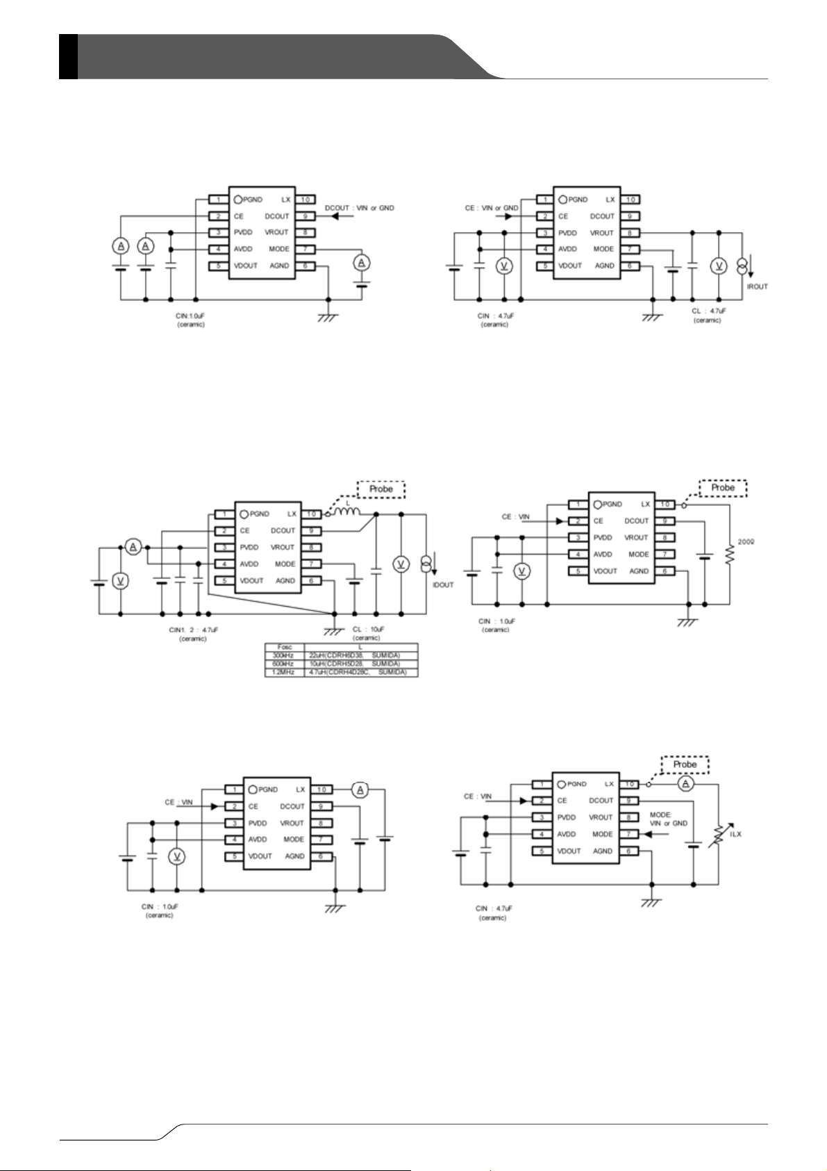
TEST CIRCUITS
Circuit 1 Supply Current, Stand-by Current, CE Current,
MODE Current
Circuit 3 Output Voltage (DC/DC), Oscillation Frequency, U.V.L.O.
Voltage, Soft-start Time, CE Voltage, Maximum Output
Current, Efficiency, (PFM Duty Cycle), (MODE Voltage)
Circuit 2 Output Voltage (VR), Load Regulation, Dropout Voltage,
Maximum Output Current, (MODE Voltage)
Circuit 4 Minimum Duty Cycle, Maximum Duty Cycle
Circuit 5 Lx ON Resistance
Circuit 6 Current Limit 1 (DC/DC)
6/41
■
)
XC9509
TEST CIRCUITS (Continued
Circuit 7 Current Limit 2 (VR), Short Circuit Current (VR) Circuit 8 Detect Voltage, Release Voltage (Hysteresis Range)
Circuit 9 VD Output Current Circuit 10 Latch Time
* For the measurement of the VDD_Sense products,
the input voltage was controlled.
Circuit 11 Off-Leak Circuit 12 Ripple Rejection Rate
*
For the measurement of the VDD_Sense products,
the input voltage was controlled.
Series
7/41
■
■
XC9509 Series
TYPICAL APPLICATION CIRCUIT
FOSC L
1.2MHz
600kHz
300kHz
MSOP-10 (TOP VIEW)
(CDRH4D28C, SUMIDA)
(CDRH5D28, SUMIDA)
(CDRH6D28, SUMIDA)
CIN CL1 CL2 (*2)
4.7μF
(ceramic, TAIYO YUDEN)
SD *1 : XB0ASB03A1BR (TOREX)
*1 The DC/DC converter of the XC9508 series automatically switches between synchronous / non-synchronous. The Schottky diode is
not normally needed. However, in cases where high efficiency is required when using the DC/DC converter during in the light load
while in non-synchronous operation, please connect a Schottky diode externally.
*2 Please be noted that the recommend value above of the CL2 may be changed depending on the input voltage value and setting voltage
value.
OPERATIONAL EXPLANATION
The XC9509 series consists of a synchronous step-down DC/DC converter, a high speed LDO voltage regulator, and a
voltage detector.
●DC/DC Converter
The series consists of a reference voltage source, ramp wave circuit, error amplifier, PWM comparator, phase
compensation circuit, output voltage adjustment resistors, driver transistor, synchronous switch, current limiter circuit,
U.V.L.O. circuit and others. The series ICs compare, using the error amplifier, the voltage of the internal voltage
reference source with the feedback voltage from the V
performed on the resulting error amplifier output, to input a signal to the PWM comparator to determine the turn-on time
during PWM operation. The PWM comparator compares, in terms of voltage level, the signal from the error amplifier
with the ramp wave from the ramp wave circuit, and delivers the resulting output to the buffer driver circuit to cause the
Lx pin to output a switching duty cycle. This process is continuously performed to ensure stable output voltage. The
current feedback circuit monitors the P-channel MOS driver transistor current for each switching operation, and
modulates the error amplifier output signal to provide multiple feedback signals. This enables a stable feedback loop
even when a low ESR capacitor, such as a ceramic capacitor, is used, ensuring stable output voltage.
(ceramic, TAIYO YUDEN)
10μF
VROUT<2.0V
ROUT>2.0V
V
OUT pin through split resistors. Phase compensation is
4.7μF (ceramic, TAIYO YUDEN)
Vdif>1.0V
Vdif<
1.0V
1.0μF (ceramic, TAIYO YUDEN)
4.7μF (ceramic, TAIYO YUDEN)
<Reference Voltage Source>
The reference voltage source provides the reference voltage to ensure stable output voltage of the DC/DC converter.
<Ramp Wave Circuit>
The ramp wave circuit determines switching frequency. The frequency is fixed internally and can be selected from
300kHz, 600 kHz and 1.2 MHz. Clock pulses generated in this circuit are used to produce ramp waveforms needed for
PWM operation, and to synchronize all the internal circuits.
<Error Amplifier>
The error amplifier is designed to monitor output voltage. The amplifier compares the reference voltage with the
feedback voltage divided by the internal split resistors. When a voltage lower than the reference voltage is fed back,
the output voltage of the error amplifier increases. The gain and frequency characteristics of the error amplifier output
are fixed internally to deliver an optimized signal to the mixer.
8/41
4.7μH
10μH
22μH
■
)
OPERATIONAL EXPLANATION (Continued
●DC/DC Converter (Continued)
<PWM/PFM>
The PWM control of the XC9509A to F series are controlled on a specified frequency from light loads through the heavy
loads. Since the frequency is specified, the composition of a noise filter etc. becomes easy. However, the efficiency at
the time of the light load may become low. The XC9509H to L series can switch in any timing between PWM control
and PWM/PFM automatic switching control. The series cannot control only PFM mode. If needed, the operation can
be set on a specified frequency; therefore, the control of the noise etc. is possible and the high efficiency at the time of
the light load during PFM control mode is possible. With the automatic PWM/PFM switching control function, the series
ICs are automatically switched from PWM control to PFM control mode under light load conditions. If during light load
conditions the coil current becomes discontinuous and on-time rate falls lower than 30%, the PFM circuit operates to
output a pulse with 30% of a fixed on-time rate from the Lx pin. During PFM operation with this fixed on-time rate,
pulses are generated at different frequencies according to conditions of the moment. This causes a reduction in the
number of switching operations per unit of time, resulting in efficiency improvement under light load conditions.
However, since pulse output frequency is not constant, consideration should be given if a noise filter or the like is
needed. Necessary conditions for switching to PFM operation depend on input voltage, load current, coil value and
other factors.
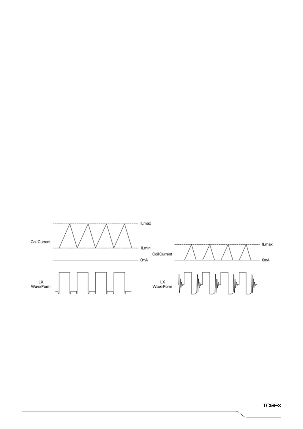
<Synchronous / Non-synchronous>
The XC9509 series automatically switches between synchronous / non-synchronous according to the state of the DC/DC
converter. Highly efficient operations are achievable using the synchronous mode while the coil current is in a
continuous state. The series enters non-synchronous operation when the built-in N-ch switching transistor for
synchronous operation is shutdown, which happens when the load current becomes low and the operation changes to a
discontinuous state. The IC can operate without an external schottky diode because the parasitic diode in the N-ch
switching transistor provides the circuit's step-down operation. However, since Vf of the parasitic diode is a high 0.6V,
the efficiency level during non-synchronous operation shows a slight decrease. Please use an external schottky diode
if high efficiency is required during light load current.
●Continuous Mode: Synchronous ●Discontinuous Mode: Non-Synchronous
XC9509
Series
9/41
■
)
XC9509 Series
OPERATIONAL EXPLANATION (Continued
●DC/DC Converter (Continued)
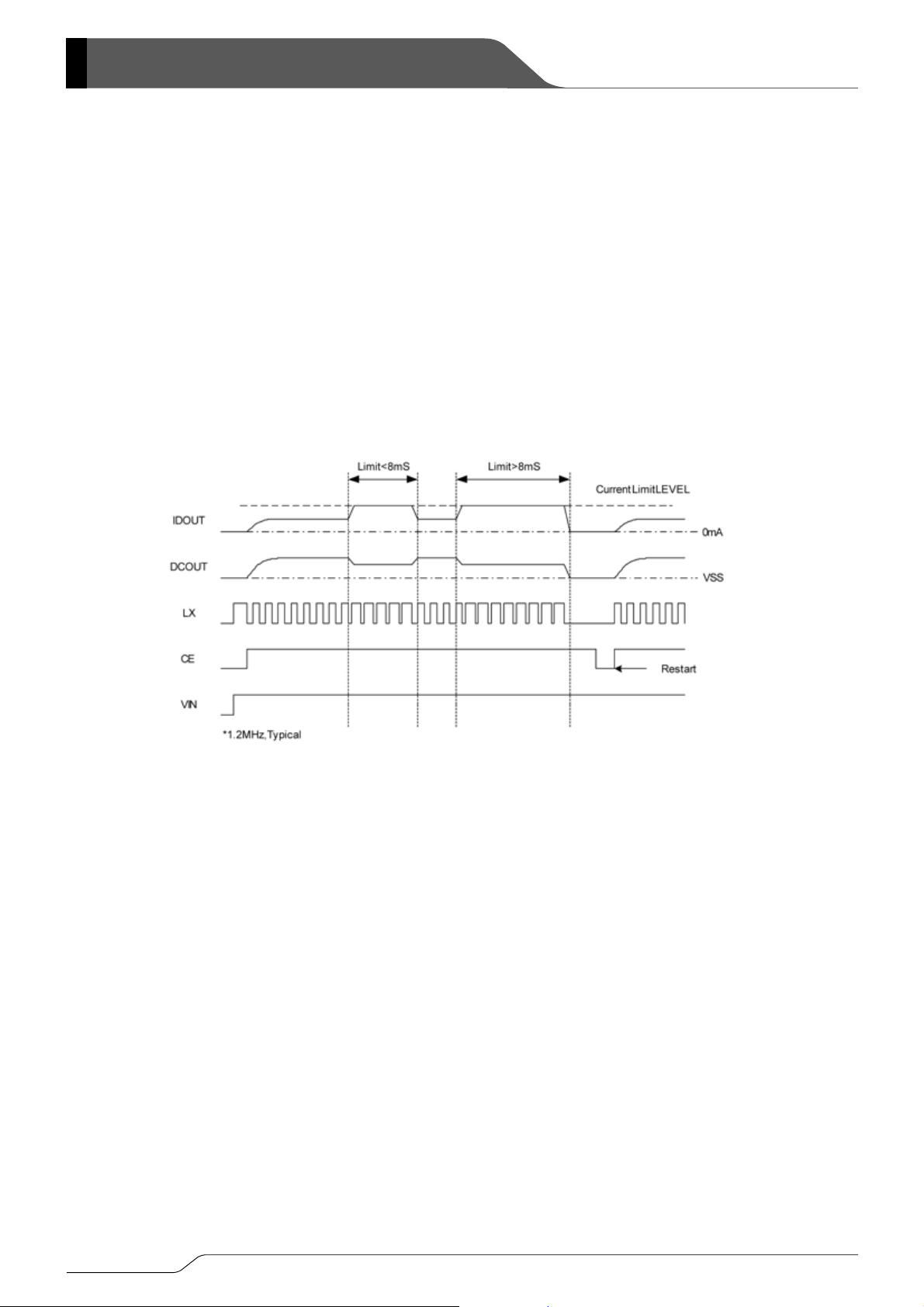
<Current Limit>
The current limiter circuit of the XC9509 series monitors the current flowing through the P-channel MOS driver transistor
connected to the Lx pin, and features a combination of the constant-current type current limit mode and the operation
suspension mode..
① When the driver current is greater than a specific level, the constant-current type current limit function operates to
●High Speed LDO Voltage Regulator
turn off the pulses from the Lx pin at any given timing.
② When the driver transistor is turned off, the limiter circuit is then released from the current limit detection state.
③ At the next pulse, the driver transistor is turned on. However, the transistor is immediately turned off in the case of
an over current state.
④ When the over current state is eliminated, the IC resumes its normal operation.
The IC waits for the over current state to end by repeating the steps ① through ③. If an over current state continues
for 8msec* and the above three steps are repeatedly performed, the IC performs the function of latching the OFF state
of the driver transistor, and goes into operation suspension mode. Once the IC is in suspension mode, operations can
be resumed by either turning the IC off via the CE pin, or by restoring power to the V
IN pin. The suspension mode does
not mean a complete shutdown, but a state in which pulse output is suspended; therefore, the internal circuitry remains
in operation. The constant-current type current limit of the XC9509 series can be set at 1.1A for MSOP-10 package
and 0.7A for USP-10 package.
*
*
<U.V.L.O. Circuit>
When the V
pulse output caused by unstable operation of the internal circuitry. When the VI
IN pin voltage becomes 1.4 V or lower, the P-channel output driver transistor is forced OFF to prevent false
N pin voltage becomes 1.8 V or higher,
switching operation takes place. By releasing the U.V.L.O. function, the IC performs the soft start function to initiate
output startup operation. The soft start function operates even when the V
IN pin voltage falls momentarily below the
U.V.L.O. operating voltage. The U.V.L.O. circuit does not cause a complete shutdown of the IC, but causes pulse
output to be suspended; therefore, the internal circuitry remains in operation.
The voltage regulator block of the XC9509 series consists of a reference voltage source, error amplifier, and current
limiter circuit. The voltage divided by split resistors is compared with the internal reference voltage by the error
amplifier. The P-channel MOSFET, which is connected to the VROUT pin, is then driven by the subsequent output
signal. The output voltage at the VR
OUT pin is controlled and stabilized by a system of negative feedback. A stable
output voltage is achievable even if used with low ESR capacitors as a phase compensation circuit is built-in.
<Reference Voltage Source>
The reference voltage source provides the reference voltage to ensure stable output voltage of the regulator.
<Error Amplifier>
The error amplifier compares the reference voltage with the signal from VR
OUT, and the amplifier controls the output of
the Pch driver transistor.
<Current Limit Circuit>
The voltage regulator block includes a combination of a constant current limiter circuit and a foldback circuit. The
voltage regulator senses output current of the built-in P channel output driver transistor inside. When the load current
reaches the current limit level, the current limiter circuit operates and the output voltage of the voltage regulator block
drops. As a result of this drop in output voltage, the foldback circuit operates, output voltage drops further and the load
current decreases. When the V
ROUT and GND pin are shorted, the load current of about 30mA flows.
10/41
■
■
)
OPERATIONAL EXPLANATION (Continued
●Voltage Detector
The detector block of the XC9509 series detects output voltage from the VDOUT pin while sensing either VDD, DCOUT, or
VROUT internally.
(N-channel Open Drain Type)
<CE Pin Function>
The operation of the XC9509 series' DC/DC converter block and voltage regulator block will enter into the shut down
mode when a low level signal is input to the CE pin. During the shut down mode, the current consumption occurs only
in the detector and is 3.0μA (TYP.), with a state of high impedance at the Lx pin and the D
operation by inputting a high level signal to the CE pin. The input to the CE pin is a CMOS input and the sink current is
0μA (TYP.).
<MODE Pin Function>
The operation of the XC9509A to C series' voltage detector block will enter into stand-by mode when a high level signal is
input to the MODE pin. When a low level signal is input, the voltage regulator block will enter into stand-by mode.
However, if the IC enters into stand-by mode via the CE pin, the voltage regulator block also shuts down. Likewise, if
the XC9509D to F series enters into stand-by mode via the CE pin, the DC/DC converter block can also shut down.
With the XC9509H to L series control can be PWM control when the MODE pin is 'H' level and PWM/PFM automatic
switching control when the MODE pin is 'L' level.
NOTES ON USE
●Application Information
1. The XC9509 series is designed for use with a ceramic output capacitor. If, however, the potential difference
between dropout voltage or output current is too large, a ceramic capacitor may fail to absorb the resulting high
switching energy and oscillation could occur on the output. If the input-output potential difference is large, connect
an electrolytic capacitor in parallel to compensate for insufficient capacitance.
COUT pin. The IC starts its
2. Spike noise and ripple voltage arise in a switching regulator as with a DC/DC converter. These are greatly
influenced by external component selection, such as the coil inductance, capacitance values, and board layout of
external components. Once the design has been completed, verification with actual components should be done.
3. When the difference between V
IN and VOUT is large in PWM control, very narrow pulses will be outputted, and there
is the possibility that some cycles may be skipped completely.
4. When the difference between V
IN and VOUT is small, and the load current is heavy, very wide pulses will be outputted
and there is the possibility that some cycles may be skipped completely: in this case, the Lx pin may not go low at all.
XC9509
Series
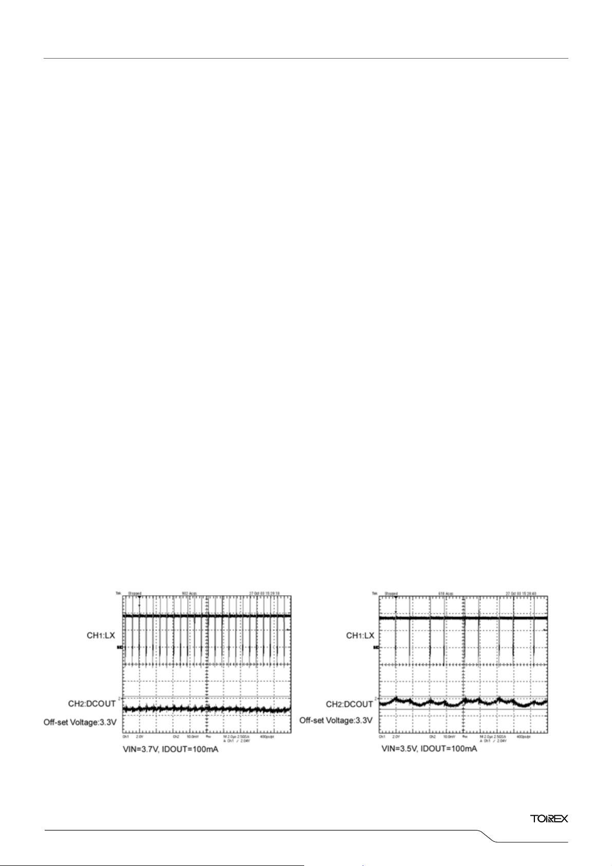
●DC/DC Waveform (3.3V, 1.2MHz)
<External Components>
L :4.7μH(CDRH4D28C,SUMIDA)
CIN :4.7μF(ceramic)
CL :10μF(ceramic)
<External Components>
<External Components>
L :4.7μH(CDRH4D28C,SUMIDA)
L :4.7μH(CDRH4D28C,SUMIDA)
CIN :4.7μF(ceramic)
CIN :4.7μF(ceramic)
CL :10μF(ceramic)
CL :10μF(ceramic)
11/41
■
)
XC9509 Series
NOTES ON USE (Continued
●DC/DC Waveform (3.3V, 1.2MHz)(Continued)
5. The IC's DC/DC converter operates in synchronous mode when the coil current is in a continuous state and
Ics = (V
Ics: Switching current from synchronous rectification to non-synchronous rectification
OnDuty: OnDuty ratio of P-ch driver transistor (
L: Coil inductance value
Fosc: Oscillation frequency
ID
PFM Duty < Step down ratio = DC
PFM Duty: 30% (TYP.)
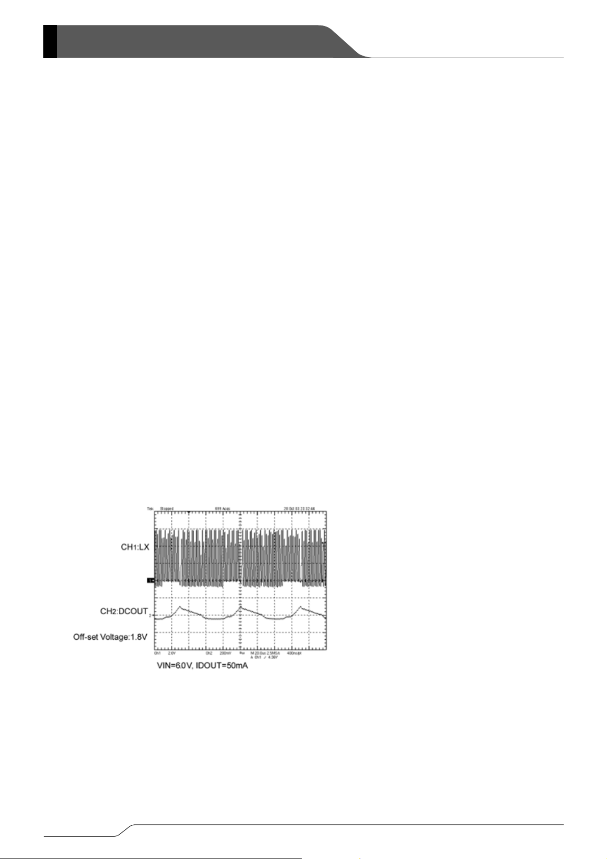
●DC/DC Waveform (1.8V, 600kHz) @ VIN=6.0V
non-synchronous mode when the coil current is in a discontinuous state. In order to maintain the load current
value when synchronous switches to non-synchronous and vise versa, a ripple voltage may increase because of
the repetition of switching between synchronous and non-synchronous. When this state continues, the increase in
the ripple voltage stops. To reduce the ripple voltage, please increase the load capacitance value or use a schottky
diode externally. When the current used becomes close to the value of the load current when synchronous
switches to non- synchronous and vise versa, the switching current value can be changed by changing the coil
inductance value. In case changes to coil inductance are to values other than the recommended coil inductance
values, verification with actual components should be done.
IN - DCOUT) x OnDuty / (L x Fosc)
.
=.step down ratio : DCOUT / VIN)
OUT: The DC/DC load current
6. When the XC9509H to L series operate in PWM/PFM automatic switching control mode, the reverse current may
become quite high around the load current value when synchronous switches to non-synchronous and vise versa
(also refer to no. 5 above). Under this condition, switching synchronous rectification and non-synchronous
rectification may be repeated because of the reverse current, and the ripple voltage may be increased to 100mV or
more. The reverse current is the current that flows in the PGND direction through the N-ch driver transistor from
the coil. The conditions, which cause this operation are as follows.
OUT / VIN x 100 (%)
Please switch to PWM control via the MODE function in cases where the load current value of the DC/DC converter
is close to synchronous
.
<External Components>
L 10μH(CDRH5D28C,SUMIDA)
CIN :4.7μF(ceramic)
CL :10μF(ceramic)
Step Down ratio: 1.8V / 6.0V = 30%<PFM Duty 31%>
12/41
■
)
NOTES ON USE (Continued
●DC/DC Waveform (3.3V, 1.2MHz) (Continued)
7. With the DC/DC converter of the IC, the peak current of the coil is controlled by the current limit circuit. Since the
RON=Rpon x P-chOnDuty / 100
+ Rnon x (1 – P-chOnDuty / 100)
peak current increases when dropout voltage or load current is high, current limit starts operating, and this can lead
to instability. When peak current becomes high, please adjust the coil inductance value and fully check the circuit
operation. In addition, please calculate the peak current according to the following formula:
Peak current: Ipk = (V
IN - DCOUT) x OnDuty / (2 x L x Fosc) + IDOUT
8. When the peak current, which exceeds limit current flows within the specified time, the built-in driver transistor is
turned off (the integral latch circuit). During the time until it detects limit current and before the built-in transistor can
be turned off, the current for limit current flows; therefore, care must be taken when selecting the rating for the coil or
the Schottky diode.
9. When VI
N is low, limit current may not be reached because of voltage falls caused by ON resistance or serial
resistance of the coil.
10. In the integral latch circuit, latch time may become longer and latch operation may not work when V
IN is 3.0V or
more.
11. Use of the IC at voltages below the recommended voltage range may lead to instability.
12. This IC and the external components should be used within the stated absolute maximum ratings in order to prevent
damage to the device.
When using IC with a regulator output at almost no load, a capacitor should be placed as close as possible between
13.
AVDD and AGND (CIN2), connected with low impedance. Please also see the recommended pattern layout on page
14 for your reference. Should it not be possible to place the input capacitor nearby, the regulated output level may
increase up to the V
DD level while the load of the DC/DC converter increases and the regulator output is at almost
no load.
14. Should the bi-directional load current of the synchronous DC/DC converter and the regulator become large, please
be careful of the power dissipation when in use. Please calculate power dissipation by using the following formula.
Pd=PdDC/DC + PdVR
DC/DC power dissipation (when in synchronous operation) : PdDC/DC = ID
OUT
2
x RON
VR power dissipation: PdVR=(DCOUT – VROUT) x IROUT
RON: ON resistance of the built-in driver transistor to the DC/DC (= 0.5Ω <TYP.>)
15. The voltage detector circuit built-in the XC9509 series internally monitor the V
DD pin voltage, the DC/DC output pin
voltage and VR output pin voltage. For the XC9509B/C/E/F/K/L series, which voltage detector circuit monitors the
DC/DC output pin voltage and the VR output pin voltage, please determine the detect voltage value (VDF) by the
following equation.
DF
≦
(Setting voltage on both the DCOUT voltage and the VROUT voltage)×85%*
V
* An assumed value of tolerance among the D
COUT voltage, the VROUT voltage, and the VD release voltage
(The VD detect voltage and hysteresis range).
XC9509
Series
13/41

■
)
XC9509 Series
NOTES ON USE (Continued
●Instructions on Pattern Layout
1. In order to stabilize V
<MSOP-10 Reference pattern layout>
possible to the AVDD & AGND pins. Should it not be possible to place the input capacitors nearby, the regulated
output level may increase because of the switching noise of the DC/DC converter.
2. Please mount each external component as close to the IC as possible.
3. Wire external components as close to the IC as possible and use thick, short connecting traces to reduce the circuit
impedance.
4. Make sure that the PCB GND traces are as thick as possible, as variations in ground potential caused by high ground
currents at the time of switching may result in instability of the DC/DC converter and have adverse influence on the
regulator output.
5. If using a Schottky diode, please connect the anode side to the AGND pin through C
caused by the noise may occur depending on the arrangement of the Schottky diode.
6. Please use the AVDD and PVDD pins with the same electric potential.
IN's voltage level, we recommend that a by-pass capacitor (CIN) be connected as close as
IN. Characteristic degradation
14/41

■
TYPICAL PERFORMANCE CHARACTERISTICS
(A) DC/DC CONVERTER
(1) Efficiency vs. Output Current
XC9509
Series
15/41

■
XC9509 Series
TYPICAL PERFORMANCE CHARACTERISTICS (Continued)
(A) DC/DC CONVERTER (Continued)
(2) Output Voltage VS. Output Current
16/41

■
TYPICAL PERFORMANCE CHARACTERISTICS (Continued)
(A) DC/DC CONVERTER (Continued)
(3) Output Voltage vs. Ripple Voltage
XC9509
Series
17/41

A
A
A
V
A
A
A
V
A
A
A
V
A
A
■
XC9509 Series
TYPICAL PERFORMANCE CHARACTERISTICS (Continued)
(A) DC/DC CONVERTER (Continued)
(4) Output Voltage vs. Ambient Temperature
1.1
1.0
DC/DC:0.9V,1.2MHz
CIN =4.7uF ,CL= 10.0uF,L= 4.7uH( CD RH4D 28C)
IDOUT =0.1m
10m
100m
VIN= 2.4V,MODE= 0
2.7
2.6
0.9
2.5
DC/DC:2.5V,1.2MHz
CIN=4.7uF,CL=10.0uF,L=4.7uH(CDRH4D28C)
IDOUT= 0.1m
10m
100m
VIN= 3.6V,MODE= 0
0.8
Output Voltage : DCOUT (V)
0.7
-50 -25 0 25 50 75 100
Ambient Temperature : Ta (℃)
DC/DC:4.0V,1.2MHz
VIN= 5.0V,M ODE= 0
4.2
4.1
CIN =4.7uF ,CL= 10.0uF,L= 4.7uH( CD RH4D 28C)
IDO UT= 0.1m
10m
100m
4.0
3.9
Output Voltage : DCOUT (V)
3.8
-50 -25 0 25 50 75 100
Ambient Temperature : Ta (℃)
2.4
Output Voltage : DCOUT (V)
2.3
-50 -25 0 25 50 75 100
Ambient Temperature : Ta (℃)
(5) Soft Start Time vs. Ambient Temperature
DC/DC:1.2MHz
VIN=6.0V,CE=0V to 6.0V,MODE=0V,IDOUT =0.1m
15
CIN=4.7uF,CL=10.0uF,L=4.7uH(CDRH4D28C)
DCOUT=0.9V
12
9
DCOUT=2.5V
6
Soft Start Time : Tss (ms)
3
DCOUT=4.0V
0
-50-250 255075100
Ambient Temperature : Ta (℃)
15
12
9
6
DC OUT =0.9V
3
Soft Start Time : Tss (ms)
0
-50 -25 0 25 50 75 100
DC/DC:600kHz
VIN= 6.0V,CE =0V to 6.0V,M ODE= 0V,IDOU T=0. 1m
CIN =4.7uF ,CL= 10.0uF,L= 10.0uH( CD RH5D 28)
DCOUT=2.5V
DC OUT =4.0V
Ambient Temperature : Ta (℃)
18/41

V
V
V
V
V
V
V
V
V
■
TYPICAL PERFORMANCE CHARACTERISTICS (Continued)
(A) DC/DC CONVERTER (Continued)
(6) DC/DC Supply Current vs. Ambient Temperature (VR: Shutdown)*
XC9509
Series
DC/DC:1.2MHz
500
400
300
200
100
DC/DC Supply Current : IDD-DC(uA)
500
400
300
CE=VIN,DCOUT=VIN,MODE=0V(VR:SHUTDOWN)
0
-50 -25 0 25 50 75 100
Ambient Temperature : Ta (℃)
DC/DC:300kHz
CE=VIN,DCOUT=VIN,MODE=0V(VR:SHUTDOWN)
DCOUT=0.9
DCOUT=0.9
DC/DC:600kHz
500
2.5
4.0
2.5
4.0
400
300
200
100
DC/DC Su pp ly Curre nt : IDD-DC(uA )
CE=VIN,DCOUT=VIN,MODE=0V(VR:SHUTDOWN)
DCOUT=0.9
2.5
4.0
0
-50 -25 0 25 50 75 100
Ambient Temperature : Ta (℃)
200
100
DC/DC Supply Current : IDD-DC(uA)
0
-50-250 255075100
Ambient Temperature : Ta (℃)
*XC9509A/B/C series only
19/41

V
V
V
V
V
A
V
■
XC9509 Series
TYPICAL PERFORMANCE CHARACTERISTICS (Continued)
(A) DC/DC CONVERTER (Continued)
(7) LX Pch/Nch ON Resistance vs. Input Voltage
DC/DC:L X Pch
1.0
)
0.8
Ω
0.6
0.4
0.2
LX Pch On Res istance (
0.0
2.0 3.0 4.0 5.0 6.0
CE= VIN,LX=VIN- 0.05V, DCOU T=0
Ta= 85
℃
Input Voltage : VIN (V)
Ta= -40
Ta= 25
℃
℃
(8) Oscillation Frequency vs. Ambient Temperature
DC/DC:2.5V,1.2MHz
1.6
1.4
CIN =4.7uF ,CL= 10.0uF,M ODE= 0V,ID OUT= 10m
VIN= 3.6
4.2
5.0
6.0
DC/DC:LX Nch
1.0
)
0.8
Ω
0.6
0.4
0.2
LX Nch On Resistance (
0.0
Ta= 85
℃
2.0 3.0 4.0 5.0 6.0
Input Voltage : VIN (V)
LX=0.05V, DCOUT=VIN
Ta= -40
℃
Ta= 25
℃
(9) U.V.L.O. Voltage vs. Ambient Temperature
MODE=0
2.2
1.8
CIN =4.7uF ,CL= 10.0uF,L= 4.7uH( CD RH4D 28C)
UVLO2( rel ease)
1.2
1.0
Oscillation Frequency:FOSC (MHz)
0.8
-50 -25 0 25 50 75 100
Ambient Temperature : Ta (℃)
1.4
1.0
UVLO Voltage : UVLO1,UVLO2 (V)
0.6
-50 -25 0 25 50 75 100
UVLO1( detect )
Ambient Temperature : Ta (℃)
20/41

■
TYPICAL PERFORMANCE CHARACTERISTICS (Continued)
(A) DC/DC CONVERTER (Continued)
(10-1) DC/DC Load Transient Response (DCOUT: 1.8V, FOSC: 1.2MHz)
(a) PWM Control
XC9509
Series
(b) PWM/PFM Automatic Switching Control* (*XC9509H/K/L Series Only)
21/41

■
XC9509 Series
TYPICAL PERFORMANCE CHARACTERISTICS (Continued)
(A) DC/DC CONVERTER (Continued)
(10-2) DC/DC Load Transient Response (*DCOUT: 3.3V, FOSC: 1.2MHz)
(a) PWM Control
(b) PMM/PFM Automatic Switching Control* (*XC9509H/K/L Series Only)
22/41

■
TYPICAL PERFORMANCE CHARACTERISTICS (Continued)
(A) DC/DC CONVERTER (Continued)
(10-3) DC/DC Load Transient Response (*DCOUT: 1.8V, FOSC: 600kHz)
(a) PWM Control
XC9509
Series
(b) PMM/PFM Automatic Switching Control* (*XC9509H/K/L Series Only)
23/41

■
XC9509 Series
TYPICAL PERFORMANCE CHARACTERISTICS (Continued)
(A) DC/DC CONVERTER (Continued)
(10-4) DC/DC Load Transient Response (DCOUT: 3.3V, FOSC: 600kHz)
(a) PWM Control
(b) PMM/PFM Automatic Switching Control* (*XC9509H/K/L Series Only)
24/41

■
TYPICAL PERFORMANCE CHARACTERISTICS (Continued)
(A) DC/DC CONVERTER (Continued)
(10-5) DC/DC Load Transient Response (DCOUT: 1.8V, FOSC: 600kHz)
(a) PWM Control
XC9509
Series
(b) PMM/PFM Automatic Switching Control* (*XC9509H/K/L Series Only)
25/41

■
XC9509 Series
TYPICAL PERFORMANCE CHARACTERISTICS (Continued)
(A) DC/DC CONVERTER (Continued)
(10-6) DC/DC Load Transient Response (DCOUT: 3.3V, FOSC: 600kHz)
(a) PWM Control
(b) PMM/PFM Automatic Switching Control* (*XC9509H/K/L Series Only)
26/41

A
A
A
A
A
A
A
A
A
A
A
A
A
A
A
A
A
A
A
A
A
A
A
A
■
TYPICAL PERFORMANCE CHARACTERISTICS (Continued)
(B) VOLTAGE REGULATOR
(1) Output Voltage vs. Input Voltage
XC9509
Series
VR:0.9V
1.3
Ta=25℃,CI N=4. 7uF,CL= 4.7uF
1.1
0.9
0.7
0.5
Output Voltage : VROUT (V)
0.3
1.2 1.4 1.6 1.8 2.0 2.2
Input Voltage : VIN (V)
VR:2.5V
2.9
Ta=25℃,CI N=4. 7uF,C L=4.7uF
2.7
2.5
2.3
2.1
Output Voltage : VROUT (V)
1.9
2.0 2.2 2.4 2.6 2.8 3.0
Input Voltage : VIN (V)
IROUT= 0m
1m
30m
100m
IROUT= 0m
1m
30m
100m
VR:0.9V
1.00
Ta=25℃,CI N=4. 7uF,CL= 4.7uF
0.95
0.90
0.85
0.80
Output Voltage : VROUT (V)
0.75
2.0 3.0 4.0 5.0 6.0
Input Voltage : VIN (V)
VR:2.5V
2.60
Ta=25℃,CI N=4. 7uF,C L=4.7uF
2.55
2.50
2.45
2.40
Output Voltage : VROUT (V)
2.35
3.0 4.0 5.0 6.0
Input Voltage : VIN (V)
IROUT= 0m
1m
30m
100m
IROUT= 0m
1m
30m
100m
VR:4.0V
4.4
Ta=25℃,CI N=4. 7uF,CL= 4.7uF
4.2
4.0
3.8
3.6
Output Voltage : VROUT (V)
3.4
3.5 3.7 3.9 4.1 4.3 4.5
Input Voltage : VIN (V)
IROUT =0m
30m
100m
4.10
4.05
4.00
3.95
1m
3.90
Output Voltage:VROUT(V)
3.85
5.0 5.2 5.4 5.6 5.8 6.0
VR:4.0V
Ta=25℃,CI N=4. 7uF,CL= 4.7uF
Input Voltage : VIN (V)
IROUT =0m
30m
100m
1m
27/41

■
XC9509 Series
TYPICAL PERFORMANCE CHARACTERISTICS (Continued)
(B) VOLTAGE REGULATOR (Continued)
(2) Output Voltage vs. Output Current (Current Limit)
Output Current : IROUT (mA) Output Current : IROUT (mA)
Output Current : IROUT (mA) Output Current : IROUT (mA)
Output Current : IROUT (mA) Output Current : IROUT (mA)
28/41

■
TYPICAL PERFORMANCE CHARACTERISTICS (Continued)
(B) VOLTAGE REGULATOR (Continued)
(3) Dropout Voltage vs. Output Current
XC9509
Series
VR:0.9V
1.0
0.8
0.6
Ta= 85
℃
25
0.4
Ta= -40
℃
0.2
Dropout Voltage : Vdif (V)
℃
0.0
0 50 100 150 200
Output Current : IROUT (mA)
VR:4.0V
0.5
0.4
0.3
CIN =4.7uF ,CL= 4.7uF
CIN =4.7uF ,CL= 4.7uF
VR:2.5V
0.5
CIN =4.7uF ,CL= 4.7uF
0.4
0.3
Ta= 25
℃
0.2
Ta= 85
℃
Dropout Voltage : Vdif (V)
0.1
Ta= -40
0.0
0 50 100 150 200
Output Current : IROUT (mA)
℃
0.2
Dropout Voltag e : Vdif (V)
Ta= 85
0.1
Ta= 25
℃
℃
0.0
0 50 100 150 200
Output Current : IROUT (mA)
Ta= -40
℃
29/41

■
XC9509 Series
TYPICAL PERFORMANCE CHARACTERISTICS (Continued)
(B) VOLTAGE REGULATOR (Continued)
(4) Output Voltage vs. Output Current
VR:0.9V
VIN= 2.4V,C IN= 4.7uF, CL=4 .7uF
1.1
1.0
0.9
0.8
0.7
Output Voltage : VROUT (V)
0.6
0 50 100 150 200
Output Current : IROUT (mA)
4.2
4.1
4.0
Ta= 85
℃
VR:4.0V
VIN =5.0V,C IN= 4.7uF, CL= 4.7uF
Ta= 25
Ta= -40
℃
Ta= -40
℃
VR:2.5V
2.7
℃
25
℃
2.6
Ta= -40
℃
2.5
2.4
Ta= 85
℃
2.3
Output Voltage : VROUT (V)
2.2
0 50 100 150 200
Output Current : IROUT (mA)
VIN= 3.5V,C IN= 4.7uF, CL=4 .7uF
Ta= 25
℃
3.9
3.8
Output Voltage : VROUT (V)
3.7
0 50 100 150 200
Output Current : IROUT (mA)
Ta= 85
℃
30/41

■
A
A
A
TYPICAL PERFORMANCE CHARACTERISTICS (Continued)
(B) VOLTAGE REGULATOR (Continued)
(5) VR Supply Current vs. Ambient Temperature (DC/DC Shutdown)*
XC9509
Series
mbient Temperature : Ta (℃)
mbient Temperature : Ta (℃)
mbient Temperature : Ta (℃)
31/41

■
XC9509 Series
TYPICAL PERFORMANCE CHARACTERISTICS (Continued)
(B) VOLTAGE REGULATOR (Continued)
(6) Output Voltage vs. Ambient Temperature
32/41

■
TYPICAL PERFORMANCE CHARACTERISTICS (Continued)
(B) VOLTAGE REGULATOR (Continued)
(7) Ripple Rejection Ratio vs. Ripple Frequency
XC9509
Series
33/41

■
XC9509 Series
TYPICAL PERFORMANCE CHARACTERISTICS (Continued)
(B) VOLTAGE REGULATOR (Continued)
(8) VR Load Transient Response
34/41

■
TYPICAL PERFORMANCE CHARACTERISTICS (Continued)
(C) VOLTAGE DETECTOR
(1) Output Current vs. Input Voltage
XC9509
Series
(2) Detect Voltage vs. Input Voltage
35/41

■
V
A
A
A
XC9509 Series
TYPICAL PERFORMANCE CHARACTERISTICS (Continued)
(C) VOLTAGE DETECTOR (Continued)
(3 ) DET ECT VOLTAG E , RE LE ASE VOLT AGE vs . AMBIENT TE MP ERAT URE
(3) Detect Voltage, Release Voltage vs. Ambient Temperature
VD:0.9V
1.5
1.3
1.1
0.9
: VDF,VDR (V)
0.7
Detect Voltage , Rel ease V oltag e
0.5
-50 -25 0 25 50 75 100
Am bient Te mp. : Ta (deg. )
mbient Temperature : Ta (℃)
5.6
5.4
5.2
VDR
VDF
VD:5.0V
DR
VD:2.5V
3.1
2.9
2.7
2.5
: VDF,V DR (V)
2.3
Detect Voltag e , R elease Voltage
2.1
-50-25 0 255075100
Am bient Te mp. : Ta (deg. )
mbient Temperature : Ta (℃)
VDR
VDF
5.0
: VDF,V DR (V)
4.8
Detect Voltage , Rel ease V oltage
4.6
-50-25 0 255075100
Ambient Temp. : Ta (deg .)
mbient Temperature : Ta (℃)
VDF
36/41

■
A
TYPICAL PERFORMANCE CHARACTERISTICS (Continued)
(D) COMMON
(1) Supply Current vs. Ambient Temperature (DC/DC & VR & VD)
XC9509
Series
mbient Temperature : Ta (℃)
(2) Shutdown Current vs. Input Voltage (3) Shutdown Current vs. Ambient Temperature
37/41

■
XC9509 Series
TYPICAL PERFORMANCE CHARACTERISTICS (Continued)
(D) COMMON (Continued)
(4) CE Pin Threshold Voltage vs. Ambient Temperature
(5) MODE Pin Threshold Voltage vs. Ambient Temperature
38/41

■
PACKAGING INFORMATION
●MSOP-10
●USP-10 Recommended Pattern Layout
2.3
XC9509
Series
●USP-10
* Soldering fillet surface is not
formed because the sides of
the pins are not plated
●USP-10 Recommended Metal Mask Design
39/41

■
XC9509 Series
MARKING RULE
●MSOP-10, USP-10
USP-10
(TOP VIEW)
MSOP-10
(TOP VIEW)
①Represents product series
MARK PRODUCT SERIES
8 XC9509xxxxxx
②Represents DC/DC control methods and MODE pin
MARK DC/DC CONTROL
MODE PIN
(H level)
MODE PIN
(L level)
PRODUCT SERIES
A XC9509Axxxxx
B XC9509Bxxxxx
C
D XC9509Dxxxxx
PWM Control
E XC9509Exxxxx
F
H XC9509Hxxxxx
K XC9509Kxxxxx
L
PWM, PFM/PWM
Manual Switch
VR: OFF VR:ON
DC/DC: OFF DC/DC: ON
PFM/PWM
Auto Switching
PWM Control
XC9509Cxxxxx
XC9509Fxxxxx
XC9509Lxxxxx
③④Represents detect voltage DC/DC,VR and VD (ex.)
MARK
③ ④
DC/DC VR VD PRODUCT SERIES
0 3 1.8V 3.3V 3.0V XC9509x03xxx
⑤Represents oscillation frequency
MARK OSCILLATION FREQUENCY PRODUCT SERIES
3 300kHz XC9509xxx3xx
6 600kHz XC9509xxx6xx
C 1.2MHz XC9509xxxCxx
⑥Represents production lot number
0 to 9,A to Z reverse character 0 to 9, A to Z repeated (G, I, J, O, Q, W excepted)
Note: No character inversion used.
40/41

XC9509
Series
1. The products and product specifications contained herein are subject to change without
notice to improve performance characteristics. Consult us, or our representatives
before use, to confirm that the information in this datasheet is up to date.
2. We assume no responsibility for any infringement of patents, patent rights, or other
rights arising from the use of any information and circuitry in this datasheet.
3. Please ensure suitable shipping controls (including fail-safe designs and aging
protection) are in force for equipment employing products listed in this datasheet.
4. The products in this datasheet are not developed, designed, or approved for use with
such equipment whose failure of malfunction can be reasonably expected to directly
endanger the life of, or cause significant injury to, the user.
(e.g. Atomic energy; aerospace; transport; combustion and associated safety
equipment thereof.)
5. Please use the products listed in this datasheet within the specified ranges.
Should you wish to use the products under conditions exceeding the specifications,
please consult us or our representatives.
6. We assume no responsibility for damage or loss due to abnormal use.
7. All rights reserved. No part of this datasheet may be copied or reproduced without the
prior permission of TOREX SEMICONDUCTOR LTD.
41/41
 Loading...