


■
■
A
■
■
XC9502 Series
ETR0702_003
2ch.Step-Up/Down DC/DC Controller ICs
GENERAL DESCRIPTION
XC9502 series is PWM controlled, PWM/PFM automatic switching controlled, multi-functional, 2 channel step-up and down
DC/DC controller ICs. With 0.9V of standard voltage supply internal, and using externally connected components, the output
1 voltage (step-up DC/DC controller) can be set freely within a range of 1.5V to 30V. Since the output 2 (step-down DC/DC
controller) has a built-in 0.9V reference voltage (accuracy ±2%), 0.9V to 6.0V can be set using external components. With
a 180kHz frequency, the size of the external components can be reduced. Switching frequencies of 300kHz and 500kHz are
also available as custom-designed products. The control of the XC9502 series can be switched between PWM control and
PWM/PFM automatic switching control using external signals. Control switches from PWM to PFM during light loads when
automatic switching is selected and the series is highly efficient from light loads through to large output currents. Noise is
easily reduced with PWM control since the frequency is fixed. The series gives freedom of control selection so that control
suited to the application can be selected. Soft-start time is internally set to 10msec (Output1) and offers protection against
in-rush currents when the power is switched. This also prevents voltage overshoot.
PPLICATIONS
●PDAs
●Palmtop computers
●Portable audio
●Various power supplies
TYPICAL APPLICATION CIRCUIT
<XC9502B092A Input : 2 cell, V
OUT①: 3.3V, VOUT②: 1.8V >
FEATURES
2ch DC/DC Controller
<Output 1: Step-Up DC/DC Controller>
Output Voltage Range
Output Current
Maximum Duty Cycle
High Efficiency
<Output 2: Step-Down DC/DC Controller>
Output Voltage Range
Output Current
Maximu Duty Cycle
High Efficiency
<Common>
Supply Voltage Range
Input Voltage Range
Oscillation Frequency
Control Method
Stand-by Function
Soft-Start Time
Package
Environmentally Friendly:
■TYPICAL PERFORMANCE
CHARACTERISTICS
☆GreenOperation-Compatible
: 1.5V ~ 30V (set by FB1 pin)
: More than 300mA
IN=1.8V,VOUT=3.3V)
(V
: 80% (TYP.)
: 83% (TYP.)
: 0.9V ~ 6.0V (set by FB2 pin)
: ≦1000mA (V
: 100% (TYP.)
: 92% (TYP.)
: 2.0V ~ 10.0V
: 0.9V ~ 10.0V
: 180kHz (±15%)
* 300kHz, 500kHz custom
: PWM or PWM/PFM selectable
: 3.0μF (MAX.)
: 10ms (internally set)
: MSOP-10, USP-10
: EU RoHS Compliant, Pb Free
IN=3.3V, VOUT=1.8V)
1/43

■
g
■
■
XC9502 Series
PIN CONFIGURATION
PIN ASSIGNMENT
1 EXT1
2 VDD
3 FB1 F B2 8
4 PW M1 PW M2 7
5 EN1 EN2 6
MSOP-10
(TOP VIEW)
(TOP VIEW)
PIN NUMBER PIN NAME FUNCTIONS
EX T2 10
MSOP-10
GND 9
EXT2
10
GND
9
FB2
8
PWM2
7
6
EN2
(BOTTOM VIEW)
USP-10
1
2
3
4
5
EXT1
VDD
FB1
PWM1
EN1
1 EXT 1 Channel 1: External Transistor Drive Pin <Connected to N-ch Power MOSFET Gate>
2 VDD Supply Voltage
3 FB1
4 PWM1
5 EN1
6 EN2
7 PWM2
8 FB2
Channel 1: Output Voltage Monitor Feedback Pin <Threshold value: 0.9V. Output voltage
can be set freely by connecting split resistors between V
Channel 1: PWM/PFM Switching Pin <Control Output 1. PWM control when connected to
V
DD, PWM / PFM auto switching when connected to Ground. >
Channel 1: Enable Pin <Connected to Ground when Output 1 is in stand-by mode.
Connected to V
Channel 2: Enable Pin <Connected to Ground when Output 2 is in stand-by mode.
Connected to V
Channel 2: PWM/PFM Switching Pin <Control Output 2. PWM control when connected to
V
DD, PWM / PFM auto switching when connected to Ground.>
Channel 2: Output Voltage Monitor Feedback Pin <Threshold value: 0.9V. Output voltage
can be set freely by connecting split resistors between V
9 GND Ground
10 EXT2/ Channel 2: External Transistor Drive Pin <Connected to P-ch Power MOSFET Gate>
PRODUCT CLASSIFICATION
●Orderin
XC9502①②③④⑤⑥‑⑦
Information
(*1)
OUT1 and Ground.>
DD when Output 1 is active. EXT1 is low when in stand-by mode.>
DD when Output 2 is active. EXT2/ is high when in stand-by mode.>
OUT2 and Ground.>
DESIGNATOR ITEM SYMBOL DESCRIPTION
①
②③
Type of DC/DC Controller B Standard type (10 pin)
Output Voltage 09
FB products → ②=0, ③=9 fixed
2 180kHz
④
Oscillation Frequency
3 300kHz (custom)
5 500kHz (custom)
AR MSOP-10 (1,000/Reel)
⑤⑥-⑦
(*1)
Packages (Order Unit)
AR-G MSOP-10 (3,000/Reel)
DR USP-10 (3,000/Reel)
DR-G USP-10 (3,000/Reel)
(*1)
The “-G” suffix indicates that the products are Halogen and Antimony free as well as being fully RoHS compliant.
2/43

■
■
A
BLOCK DIAGRAM
BSOLUTE MAXIMUM RATINGS
PAR AMETER SYMBOL RATINGS UNITS
XC9502
Series
Ta =2 5℃
VDD Pin Voltage VDD - 0.3 ~ 12.0 V
FB1, 2 Pin Voltage VFB - 0.3 ~ 12.0 V
EN1, 2 Pin Voltage VEN - 0.3 ~ 12.0 V
PWM1, 2 Pin Voltage VPWM - 0.3 ~ 12.0 V
EXT1, 2 Pin Voltage VEXT - 0.3 ~ VDD + 0.3 V
EXT1, 2 Pin Current IEXT ± 100 mA
MSOP-10 150
Power Dissipation
USP-10
Operating Temperature Range Topr - 40 ~ + 85
Storage Temperature Range Tstg
Pd
150
- 55 ~ + 125
mW
O
C
O
C
* Voltage is all ground standardized.
3/43

■
XC9502 Series
ELECTRICAL CHARACTERISTICS
XC9502B092 Common Characteristics
PARAMETER SYMBOL CONDITIONS MIN. TYP. MAX. UNITS CIRCUIT
Supply Voltage (*1) VDD 2.0 − 10.0 V
Maximum Input Voltage VIN 10.0 − − V
VOUT1 0.9 − − V VDD≧2.0V, IOUT1, 2=1mA
DD≠VOUT1
Output Voltage Range (*3) VOUTSET
Supply Current 1 IDD1
Supply Current 1-1 IDD1-1
Supply Current 1-2 IDD1-2
Supply Current 1-3 IDD1-3
Supply Current 1-4 IDD1-4
Supply Current 2 IDD2
Stand-by Current ISTB
V
IN≧0.9V, IOUT1, 2=1mA
V
DD=VOUT1
V
FB1, 2=0V
EN1=3.0V, EN2=0V, FB1=0V
EN2=3.0V, EN1=0V, FB2=0V
FB1=0V, FB2=1.0V
FB1=1.0V, FB2=0V
FB1, 2=1.0V
Same as I
DD1, EN1=EN2=0V
Oscillation Frequency FOSC Same as IDD1 153 180 207 kHz
EN1, 2 "High" Voltage VENH FB1, 2=0V 0.65 − − V
EN1, 2 "Low" Voltage VENL
EN1, 2 "High" Current IENH
EN1, 2 "Low" Current IENL
PWM1, 2 "High" Current IPWMH
PWM1, 2 "Low" Current IPWML
FB1, 2 "High" Current IFBH
FB1, 2 "Low" Current
Unless otherwise stated, VDD=3.0V, PWM1, 2=3.0V, EN1, 2 =3.0V
Output 1 Characteristics: Step-Up Controller
FBL
V
FB1, 2=0V
EN1, 2=3.0V
EN1, 2=0V, FB1, 2=3.0V
FB1, 2=3.0V, PWM=3.0V
FB1, 2=3.0V, PWM=0V
FB1, 2=3.0V
FB1, 2=1.0V
PARAMETER SYMBOL CONDITIONS MIN. TYP. MAX. UNITS CIRCUIT
FB1 Voltage VFB1 VDD=3.0V, VIN=1.5V, IOUT1=10mA 0.882 0.900 0.918 V
Using Tr: 2SD1628
OUT1=1.0mA, RFB11=200kΩ, RFB12=75kΩ
Operation Start Voltage1 (*2) VST1-1
I
V
DD≠VOUT1: IOUT1=1mA − − 2.0 V
Oscillation Start-up Voltage1 VST2-1 FB1=0V
Maximum Duty Ratio1 MAXDTY1 Same as IDD1 75 80 85 %
Minimum Duty Ratio1 MINDTY1 Same as IDD2
PFM Duty Ratio1 PFMDTY1 No Load, VPWM1=0V 22 30 38 %
OUT1=30mA,
Efficiency 1 (*4) EFFI1
Soft-Start Time1 TSS1
I
N-ch MOSFET: XP161A1355P
V
OUT1×0.95V, EN1=0V→0.65V
EXT1 "High" ON Resistance REXTBH1 FB1=0, EXT1=VDD-0.4V
EXT1 "Low" ON Resistance REXTBL1 EN1=FB2=0V, EXT1=0.4V
PWM1 "High" Voltage
PWM1 "Low" Voltage
Unless otherwise stated, VDD=EN1=PWM1=3.0V, EN2=PWM2=GND, EXT2=OPEN, FB2=OPEN, VIN=1.8V
Output 2 Characteristics: Step-Down Controller
PWMH1 No Load 0.65
V
PWMH1 No Load
V
PARAMETER SYMBOL CONDITIONS MIN. TYP. MAX. UNITS CIRCUIT
FB 2 Voltage VFB2 VIN=3.0V, IOUT2=10mA 0.882 0.900 0.918 V
Minimum Operating Voltage VINmin
Maximum Duty Ratio 2 MAXDTY2 Same as IDD1 100
Minimum Duty Ratio 2 MINDTY2 Same as IDD2
PFM Duty Ratio 2 PFMDTY2 No Load, VPW M2=0V 22 30 38 %
OUT2=250mA
Efficiency 2 (*4) EFFI2
Soft-Start Time 2 TSS2
I
P-ch MOSFET: XP162A12A6P
V
OUT2×0.95V, EN2=0V→0.65V
EXT2 "High" ON Resistance REXTBH2 EN2=0, EXT2=VDD-0.4V
EXT2 "Low" ON Resistance REXTBL2 FB2=0V, EXT2=0.4V
PWM2 "High" Voltage VPWMH2 No Load 0.65 − − V
PWM2 "Low" Voltage
Unless otherwise stated, VDD=EN2=PWM2=3.0V, PWM1=EN1=GND, EXT1=OPEN, FB1=OPEN, VIN=5.0V
NOTE:
*1 : Although the IC's step-up operations start from a VDD of 0.8V, the output voltage and switching frequency are stabilized at VDD
≧
2.0V. Therefore, a V
*2 : Although the IC's switching operations start from a V
(FB1) should be connected to V
chip disable. Once output voltage V
*3 : Please be careful not to exceed the breakdown voltage level of the external components.
PWMH2
V
DD of more than 2.0V is recommended when VDD is supplied from VIN or other power sources.
No Load
IN of 0.9V, the IC's power supply pin (VDD) and output voltage monitor pin
OUT1. With operations from VIN=0.9V, the 2nd channel's (output 2) EN2 pin should be set to
OUT1 is more than 2.0V, the EN2 pin should be set to chip enable.
*4 : EFFI={ [ (Output voltage) × (Output current) ] / [ (Input voltage) × (Input current) ] } ×100
OUT2 0.9 − VIN V
V
VOUT1 2.0 − 10.0 V
OUT2 0.9 − VIN V
V
(FOSC=180kHz)
− 70 160 μA
− 60 120 μA
− 50 110 μA
− 70 160 μA
− 60 130 μA
− 60 130 μA
− 1.0 3.0 μA
− − 0.20 V
− − 0.50 μA
− − -0.50 μA
− − 0.50 μA
− − -0.50 μA
− − 0.50 μA
− − -0.50 μA
− − 0.9 V
− −
− −
− 85 − %
5.0 10.0 20.0 ms
−
−
− −
− −
− −
− 92 − %
5.0 10.0 20.0 ms
−
−
− −
0.8 V
0 %
28 47
22 30
− −
0.20 V
2.0 V
− −
0 %
28 47
22 30
0.20 V
Ω
Ω
V
%
Ω
Ω
Ta =2 5℃
①
①
①
②
③
③
③
③
③
③
③
③
③
③
③
③
③
③
③
③
Ta =2 5℃
④
②
①
③
③
③
⑤
⑤
⑤
⑥
⑥
⑤
⑤
Ta =2 5℃
⑦
①
③
③
⑧
⑧
⑧
⑥
⑥
⑧
⑧
4/43

XC9502
Series
■ELECTRICAL CHARACTERISTICS (Continued)
Ω
Ω
V
%
Ω
Ω
Ta =2 5℃
①
①
①
②
③
③
③
③
③
③
③
③
③
③
③
③
③
③
③
③
Ta =2 5℃
④
②
①
③
③
③
⑤
⑤
⑤
⑥
⑥
⑤
⑤
Ta =2 5℃
⑦
①
③
③
⑧
⑧
⑧
⑥
⑥
⑧
⑧
XC9502B093
Common Characteristics
(FOSC=300kHz)
PARAMETER SYMBOL CONDITIONS MIN. TYP. MAX. UNITS CIRCUIT
Supply Voltage (*1) VDD 2.0 − 10.0 V
Maximum put Voltage VIN 10.0 − − V
VOUT1 0.9 − − V VDD≧0V, IOUT1, 2=1mA
Output Voltage Range (*3) VOUTSET
Supply Current 1 IDD1
Supply Current 1-1 IDD1-1
Supply Current 1-2 IDD1-2
Supply Current 1-3 IDD1-3
Supply Current 1-4 IDD1-4
Supply Current 2 IDD2
Stand-by Current ISTB
V
IN≧0.9V, IOUT1, 2=1mA
V
DD=VOUT1
V
FB1, 2=0V
EN1=3.0V, EN2=0V, FB1=0V
EN2=3.0V, EN1=0V, FB2=0V
FB1=0V, FB2=1.0V
FB1=1.0V, FB2=0V
FB1, 2=1.0V
Same as I
DD1, EN1=EN2=0V
V
OUT2 0.9 − VIN V
VOUT1 2.0 − 10.0 V
OUT2 0.9 − VIN V
V
− 100 190 μA
− 80 150 μA
− 60 120 μA
− 100 190 μA
− 70 150 μA
− 70 150 μA
− 1.0 3.0 μA
DD≠VOUT1
Oscillation Frequency FOSC Same as IDD1 255 300 345 kHz
EN1, 2 "High" Voltage VENH
EN1, 2 "Low" Voltage VENL
EN1, 2 "High" Current IENH
EN1, 2 "Low" Current IENL
PWM1, 2 "High" Current IPWMH
PWM1, 2 "Low" Current IPWML
FB1, 2 "High" Current IFBH
FB1, 2 "Low" Current
Output 1 Characteristics: Step-Up Controller
=
FBL FB1, 2=1.0V
V
FB1, 2=0V
FB1, 2=0V
EN1, 2=3.0V
EN1, 2=0V, FB1, 2=3.0V
FB1, 2=3.0V, PWM=3.0V
FB1, 2=3.0V, PWM=0V
FB1, 2=3.0V
=
=
0.65 − − V
− − 0.20 V
− − 0.50 μA
− − -0.50 μA
− − 0.50 μA
− − -0.50 μA
− − 0.50 μA
− − -0.50 μA
PARAMETER SYMBOL CONDITIONS MIN. TYP. MAX. UNITS CIRCUIT
FB1 Voltage VFB1 VDD=3.0V, VIN=1.5V, IOUT1=10mA 0.882 0.900 0.918 V
Using Tr: 2SD1628
OUT1=1.0mA, RFB11=200kΩ, RFB12=75kΩ
Operation Start Voltage (*2) VST1-1
I
V
DD≠VOUT1: IOUT1=1mA − − 2.0 V
Oscillation Start Voltage2 VST2-1 FB1=0V
− − 0.9 V
− −
0.8 V
Maximum Duty Ratio MAXDTY1 Same as IDD1 75 80 85 %
Minimum Duty Ratio MINDTY1 Same as IDD2
− −
0 %
PFM Duty Ratio PFMDTY1 No Load, VPW M1=0V 22 30 38 %
OUT=130mA
Efficiency (*4) EFFI1
Soft-Start Time TSS1
EXT1 "High" ON Resistance REXTBH1 FB1=0, EXT1=VDD-0.4V
EXT1 "Low" ON Resistance REXTBL1 EN1=FB2=0V, EXT1=0.4V
PWM1 "High" Voltage
PWM1 "Low" Voltage
Unless otherwise stated, VDD=EN1=PWM1=3.0V, EN2=PWM2=GND, EXT2=OPEN, FB2=OPEN, VIN=1.8V
Output 2 Characteristics: Step-Down Controller
PWMH1 No Load 0.65
V
PWMH1 No Load
V
I
N-ch MOSFET: XP161A1355P
V
OUT1×0.95V, EN1=0V→0.65V
− 85 − %
5.0 10.0 20.0 ms
−
−
28 47
22 30
− −
− −
0.20 V
PARAMETER SYMBOL CONDITIONS MIN. TYP. MAX. UNITS CIRCUIT
FB2 Voltage VFB2 VIN=3.0V, IOUT2=10mA 0.900 0.900 0.900 V
Minimum Operating Voltage VINmin
Maximum Duty Ratio 2 MAXDTY2 Same as IDD1 100
Minimum Duty Ratio 2 MINDTY2 Same as IDD2
− −
− −
− −
2.0 V
0 %
PFM Duty Ratio 2 PFMDTY2 No Load, VPWM2=0V 22 30 38 %
OUT2=250mA
Efficiency 2 (*4) EFFI2
Soft-Start Time 2 TSS2
EXT2 "High" ON Resistance REXTBH2 EN2=0, EXT2=VDD-0.4V
EXT2 "Low" ON Resistance REXTBL2 FB2=0V, EXT2=0.4V
I
P-ch MOSFET: XP162A12A6P
V
OUT2×0.95V, EN2=0V→0.65V
− 92 − %
5.0 10.0 20.0 ms
−
−
28 47
22 30
PWM2 "High" Voltage VPWMH2 No Load 0.7 − − V
PWM2 "Low" Voltage
Unless otherwise stated, VDD=EN2=PWM2=3.0V, PWM1=EN1=GND, EXT1=OPEN, FB1=OPEN, VIN=5.0V
*1 : Although the IC's step-up operations start from a V
NOTE:
≧ 2.0V. Therefore, a V
*2 : Although the IC's switching operations start from a V
(FB1) should be connected to V
chip disable. Once output voltage V
*3 : Please be careful not to exceed the breakdown voltage level of the external components.
*4 : EFFI={ [ (output voltage) × (output current) ] / [ (input voltage) × (input current) ] } × 100
PWMH2
V
DD of more than 2.0V is recommended when VDD is supplied from VIN or other power sources.
No Load
DD of 0.8V, the output voltage and switching frequency are stabilized at VDD
IN of 0.9V, the IC's power supply pin (VDD) and output voltage monitor pin
OUT1. With operations from VIN=0.9V, the 2nd channel's (output 2) EN2 pin should be set to
OUT1 is more than 2.0V, the EN2 pin should be set to chip enable.
− −
0.20 V
5/43

XC9502 Series
■ELECTRICAL CHARACTERISTICS (Continued)
XC9502B095
Common Characteristics
PARAMETER SYMBOL CONDITIONS MIN. TYP. MAX. UNITS CIRCUIT
Supply Voltage (*1) VDD 2.0 − 10.0 V
Maximum Input Voltage VIN 10.0 − − V
VOUT1 0.9 − − V
V
OUT2 0.9 − VIN V
VOUT1 2.0 − 10.0 V
OUT2 0.9 − VIN V
V
Output Voltage Range (*3) VOUT SET
Supply Current 1 IDD1
Supply Current 1-1 IDD1-1
Supply Current 1-2 IDD1-2
Supply Current 1-3 IDD1-3
Supply Current 1-4 IDD1-4
Supply Current 2 IDD2
Stand-by Current ISTB
VDD≧2.0V, IOUT1, 2=1mA
DD≠VOUT1
V
IN≧0.9V, IOUT1, 2=1mA
V
DD=VOUT1
V
FB1, 2=0V
EN1=3.0V, EN2=0V, FB1=0V
EN2=3.0V, EN1=0V, FB2=0V
FB1=0V, FB2=1.0V
FB1=1.0V, FB2=0V
FB1, 2=1.0V
Same as I
DD1, EN1=EN2=0V
Oscillation Frequency FOSC Same as IDD1 425 500 575 kHz
EN1, 2 "High" Voltage VENH
EN1, 2 "Low" Voltage VENL
EN1, 2 "High" Current IENH
EN1, 2 "Low" Current IENL
PWM1, 2 "High" Current IPWMH
PWM1, 2 "Low" Current IPWML
FB1, 2 "High" Current IFBH
FB1, 2 "Low" Current
Unless otherwise stated, VDD=3.0V, PWM1, 2=3.0V, EN1, 2 =3.0V
Output 1 Characteristics: Step-Up Controller
FBL
V
FB1, 2=0V
FB1, 2=0V
EN1, 2=3.0V
EN1, 2=0V, FB1, 2=3.0V
FB1, 2=3.0V, PWM=3.0V
FB1, 2=3.0V, PWM=0V
FB1, 2=3.0V
FB1, 2=1.0V
PARAMETER SYMBOL CONDITIONS MIN. TYP. MAX. UNITS CIRCUIT
FB 1 Voltage VFB1 VDD=3.0V, VIN=1.5V, IOUT1=10mA 0.882 0.900 0.918 V
Using Tr: 2SD1628
OUT1=1.0mA, RFB11=200kΩ, RFB12=75kΩ
Operation Start Voltage 1 (*2) VST1-1
I
V
DD≠VOUT1: IOUT1=1mA − − 2.0 V
Oscillation Start Voltage 2 VST2-1 FB1=0V
Maximum Duty Ratio 1 MAXDTY1 Same as IDD1 75 80 85 %
Minimum Duty Ratio 1 MINDTY1 Same as IDD2
PFM Duty Ratio 1 PFMDTY1 No Load, VPWM1=0V 22 30 38 %
OUT=130mA
Efficiency 1 (*4) EFFI1
Soft-Start Time 1 TSS1
I
N-ch MOSFET: XP161A1355P
V
OUT1×0.95V, EN1=0V→0.65V
EXT1 "High" ON Resistance REXTBH1 FB1=0, EXT1=VDD-0.4V
EXT1 "Low" ON Resistance REXTBL1 EN1=FB2=0V, EXT1=0.4V
PWM1 "High" Voltage
PWM1 "Low" Voltage
Unless otherwise stated, V
Output 2 Characteristics: Step-Down Controller
DD=EN1=PWM1=3.0V, EN2=PWM2=GND, EXT2=OPEN, FB2=OPEN, VIN=1.8V
PWMH1 No Load 0.65
V
PWMH1 No Load
V
PARAMETER SYMBOL CONDITIONS MIN. TYP. MAX. UNITS CIRCUIT
FB 2 Voltage VFB2 VIN=3.0V, IOUT2=10mA 0.882 0.900 0.918 V
Minimum Operating Voltage VINmin
Maximum Duty Ratio 2 MAXDTY2 Same as IDD1 100
Minimum Duty Ratio 2 MINDTY2 Same as IDD2
PFM Duty Ratio 2 PFMDTY2 No Load, VPW M2=0V 22 30 38 %
OUT2=250mA
Efficiency 2 (*4) EFFI2
Soft-Start Time 2 TSS2
I
P-ch MOSFET: XP162A12A6P
V
OUT2×0.95V, EN2=0V→0.65V
EXT2 "High" ON Resistance REXTBH2 EN2=0, EXT2=VDD-0.4V
EXT2 "Low" ON Resistance REXTBL2 FB2=0V, EXT2=0.4V
PWM2 "High" Voltage VPWMH2 No Load 0.65 − − V
PWM2 "Low" Voltage
Unless otherwise stated, V
*1 : Although the IC's step-up operations start from a VDD of 0.8V, the output voltage and switching frequency are stabilized at VDD
NOTE:
≧ 2.0V. Therefore, a V
*2 : Although the IC's switching operations start from a V
(FB1) should be connected to V
chip disable. Once output voltage V
*3 : Please be careful not to exceed the breakdown voltage level of the external components.
*4 : EFFI={ [ (output voltage) × (output current) ] / [ (input voltage) × (input current) ] } × 100
DD=EN2=PWM2=3.0V, PWM1=EN1=GND, EXT1=OPEN, FB1=OPEN, VIN=5.0V
PWMH2
V
DD of more than 2.0V is recommended when VDD is supplied from VIN or other power sources.
No Load
IN of 0.9V, the IC's power supply pin (VDD) and output voltage monitor pin
OUT1. With operations from VIN=0.9V, the 2nd channel's (output 2) EN2 pin should be set to
OUT1 is more than 2.0V, the EN2 pin should be set to chip enable.
(FOSC=500kHz)
− 130 250 μA
− 110 220 μA
− 80 150 μA
− 130 240 μA
− 90 190 μA
− 90 190 μA
− 1.0 3.0 μA
0.65 − − V
− − 0.20 V
− − 0.50 μA
− − -0.50 μA
− − 0.50 μA
− − -0.50 μA
− − 0.50 μA
− − -0.50 μA
− − 0.9 V
− −
− −
− 83 − %
5.0 10.0 20.0 ms
−
−
28 47
22 30
− −
− −
− −
− −
− −
− 91 − %
5.0 10.0 20.0 ms
−
−
28 47
22 30
− −
0.8 V
0 %
Ω
Ω
V
0.20 V
2.0 V
%
0 %
Ω
Ω
0.20 V
Ta =2 5℃
①
①
①
②
③
③
③
③
③
③
③
③
③
③
③
③
③
③
③
③
Ta =2 5℃
④
②
①
③
③
③
⑤
⑤
⑤
⑥
⑥
⑤
⑤
Ta =2 5℃
⑦
①
③
③
⑧
⑧
⑧
⑥
⑥
⑧
⑧
6/43

■
XC9502
Series
OPERATIONAL EXPLANATION
The XC9502 series are multi-functional, 2 channel step-up and down DC/DC converter controller ICs with built-in high speed,
low ON resistance drivers.
<Error Amp. >
The error amplifier is designed to monitor the output voltage and it compares the feedback voltage (FB) with the reference
voltage. In response to feedback of a voltage lower than the reference voltage, the output voltage of the error amp.
decreases.
<OSC Generator>
This circuit generates the switching frequency, which in turn generates the reference clock.
<Ramp Wave Generator 1, 2>
The ramp wave generator generates a saw-tooth waveform based on outputs from the Phase Shift Generator.
<PWM Comparator 1, 2>
The PWM comparator compares outputs from the error amp. and saw-tooth waveform. When the voltage from the error
amp's output is low, the external switch will be set to ON.
<PWM/PFM Controller 1, 2>
This circuit generates PFM pulses.
Control can be switched between PWM control and PWM/PFM automatic switching control using external signals.
The PWM/PFM automatic switching mode is selected when the voltage of the PWM1 (2) pin is less than 0.2V, and the control
switches between PWM and PFM automatically depending on the load. As the PFM circuit generates pulses based on
outputs from the PWM comparator, shifting between modes occurs smoothly. PWM control mode is selected when the
voltage of the PWM1 (2) pin is more than 0.65V. Noise is easily reduced with PWM control since the switching frequency is
fixed. Control suited to the application can easily be selected which is useful in audio applications, for example, where
traditionally, efficiencies have been sacrificed during stand-by as a result of using PWM control (due to the noise problems
associated with the PFM mode in stand-by).
<Vref with Soft Start 1, 2>
The reference voltage, Vref (FB pin voltage)=0.9V, is adjusted and fixed by laser trimming (for output voltage settings, please
refer to the notes on next page). To protect against inrush current, when the power is switched on, and also to protect against
voltage overshoot, soft-start time is set internally to 10ms. It should be noted, however, that this circuit does not protect the
load capacitor (C
L) from inrush current. With the Vref voltage limited and depending upon the input to the error amps, the
operation maintains a balance between the two inputs of the error amps and controls the EXT pin's ON time so that it doesn't
increase more than is necessary.
<Chip Enable Function>
This function controls the operation and shutdown of the IC. When the voltage of the EN1 or EN2 pins is 0.2V or less, the
mode will be chip disable, the channel's operations will stop and the EXT1 pin will be kept at a low level (the external N-ch
MOSFET will be OFF) and the EXT2 pin will be kept at a high level (the external P-type MOSFET will be OFF). When both
EN1 and EN2 are in a state of chip disable, current consumption will be no more than 3.0μA.
When the EN1 or EN2 pin's voltage is 0.65V or more, the mode will be chip enable and operations will recommence. With
soft-start, 95% of the set output voltage will be reached within 10mS (TYP.) from the moment of chip enable.
Although IC starts oscillation from a V
should be connected to V
supply voltage of V
V
OUT1 is more than 2.0V. For power supply voltages of VDD<2.0V, oscillation may occur irrespective of the FB pin voltage.
OUT1. The start-up sequence for EN1 and EN2 is required when operations begin with a power
DD=0.9V, and channel two's (output 2) EN2 pin should be set to chip disable and turn it to enable when
IN of 0.9V, the IC's power supply pin (VDD) and the output voltage monitor pin (FB1)
Should this happen, you may find that output voltage will be higher than the set voltage. The FB pin voltage and the
reference voltage Vref will be compared and output voltage will be controlled when the power supply voltage is V
DD>2.0V or
more. With power supply voltages of VDD>2.0V, the start-up sequence for EN1 and EN2 will not be required.
7/43

XC9502 Series
■OPERATIONAL EXPLANATION (Continued)
<Setting of Output Voltage>
Output voltage can be set by adding external split resistors. Output voltage is determined by the following equation, based
on the values of RFB11 (RFB21) and RFB12 (RFB22). The sum of RFB11 (RFB21) and RFB12 (RFB22) should normally be 1MΩor
less.
The value of C
equal to 12kHz. Adjustments are required from 1kHz to 50kHz depending on the application, value of inductance (L), and
value of load capacity (C
[Example of Calculation]
When R
[Typical Example]
VOUT
(V)
FB1 (CFB2), speed-up capacitor for phase compensation, should be fzfb= 1 / (2
L).
FB11=200k
RFB11
(kΩ)
Ω
and RFB12=75kΩ, VOUT1=0.9×(200k+75k) / 75k=3.3V.
RFB12
(kΩ)
1.0 30 270 430 2.5 390 220 33 8.0 120 15 100
1.5 220 330 62 2.7 360 180 33 12.0 160 13 82
1.8 220 220 62 3.0 560 240 24 - - - -
2.0 330 270 39 3.3 200 75 62 - - - -
2.2 390 270 33 5.0 82 18 160 - - - -
The same method can be also adopted for channel two (output 2).
[External Components]
Output 1 (Step-Up DC/DC controller)
Tr 1 :* MOSFET
XP161A1355PR (N-ch Power MOSFET, TOREX)
SD 1: MA2Q737 (Schottky, MATSUSHITA)
L 1: 10μH (CDRH5D28, SUMIDA, FOSC = 500kHz)
C
Tr : * NPN MOSFET 2SD1628 (SANYO)
RB1 : 500Ω ( Adjust in accordance with load & Tr.'s HFE.)
C
Set according to the equation below:
Note: V
GS Breakdown Voltage of this Tr. is 8V so
please be careful with the power supply voltage.
For 6V power supply voltage, XP161A1265PR
which V
recommended. V
GS breakdown voltage is 12V is
ST1 of XP161A1355PR is 1.2V
(MAX.) and that of XP161A1265PR is 1.5V (MAX.)
CMS02 (Schottky, TOSHIBA)
15μH (CDRH5D28, SUMIDA, FOSC = 300kHz)
22μH (CDRH5D28, SUMIDA, FOSC = 180kHz)
L1 : 16V, 47μF (Tantalum)
Increase capacity according to the equation below
when the step-up voltage ratio is large and output
current is high.
C=(C
L standard value)
×
(IOUT1(mA)/300mA×VOUT1/VIN)
Set according to the equation below:
R
B1
≦
(VIN-0.7) x hFE / IC-REXTBH
B1 : 2200pF (Ceramic)
C
B1
≦
(2πx RB2 x FOSC x 0.7)
CFB1
(pF)
OUT=0.9
V
VOUT
×
(RFB11+RFB12) /RFB12
RFB11
(V)
(kΩ)
×π×
CFB1×RFB11) which is
RFB12
(kΩ)
CFB1
(pF)
VOUT
(V)
RFB11
(kΩ)
RFB12
(kΩ)
CFB1
(pF)
Output 2 (Step-Down DC/DC controller)
Tr 2 : * MOSFET
XP162A12A6P (P-ch Power MOSFET, TOREX)
Note: V
GS Breakdown Voltage of this Tr. is 12V
so please be careful with the power supply
voltage.
SD 2: MA2Q737 (Schottky, MATSUSHITA)
CMS02 (Schottky, TOSHIBA)
L 2:10μH (CDRH5D28, SUMIDA, FOSC = 500kHz)
22μH (CDRH5D28, SUMIDA, FOSC = 300kHz)
47μH (CDRH5D28, SUMIDA, FOSC = 180kHz)
CL1 : 16V, 47μF (Tantalum)
Increase capacity according to the equation below
when the step-up voltage ratio is large and output
current is high.
C=(C
L standard value)
×
(IOUT2 (mA)/500mA×VOUT2/VIN
Tr : * PNP MOSFET 2SA1213 (SANYO)
RB1 : 500Ω ( Adjust in accordance with load & Tr.'s HFE.)
Set according to the equation below:
R
B2
≦
(VIN-0.7) x hFE / IC-REXTBH
B1 : 2200pF (Ceramic)
C
Set according to the equation below:
C
B2
≦
(2πx RB2 x FOSC x 0.7)
8/43

■
TEST CIRCUITS
Circuit 1
Circuit ①
V
OUT1
R
FB11
C
L1
R
FB12
SBD1
C
SBD2
L2
V
OUT2
510
Ω
FB21
R
C
FB2
C
L2
R
L2
R
FB22
L1
V
510
Ω
NPN
Tr1
FB1
2200pF
1μF
IN
1 EXT1
EXT2 10
2 VDD
GND 9
3 FB1 FB2 8
4 PWM1 PWM2 7
5 EN1 EN2 6
PNP
Tr2
C
IN
2200pF
Circuit ⑤
Circuit 5
V
L
R
Circuit 2
Circuit ②
V
OUT1
FB11
R
C
L1
R
FB12
C
SBD1
FB1
L1
V
510
Ω
NPN
Tr1
2200pF
IN
1 EXT1
EXT2 10
2 VDD
GND 9
3 FB1 FB2 8
4 PWM1 PWM2 7
5 EN1 EN2 6
PNP
Tr2
IN
C
2200pF
SBD2
L2
V
OUT2
510
Ω
R
FB21
C
FB2
C
L2
R
L2
R
FB22
Circuit 6
Circuit ⑥
OSC
Circuit 3
Circuit ③
Circuit 7
Circuit ⑦
1 EXT1
A
OSC
1μF
V
A
A
V
DD
FB1
V
PWM1VEN1
A
EXT2 10
2 VDD
GND 9
3 FB1 FB2 8
4 PWM1 PWM2 7
5 EN1 EN2 6
A
A
V
PWM2
V
EN2
OSC
A
V
FB2
A
V
IN
C
IN
Circuit 4
Circuit ④ Circuit ⑧
V
OUT1
C
V
L1
L
R
Nch
L1
MOSFET1
1 EXT1
SBD1
EXT2 10
1μF
2 VDD
3 FB1 FB2 8
4 PWM1 PWM2 7
5 EN1 EN2 6
C
IN
DD
V
GND 9
V
IN
C
IN
Circuit 8
A
V
IN
XC9502
Series
OUT1
200k
C
L1
75k
1μF
Ω
Ω
V
DD
1 EXT1
2 VDD
3 FB1 FB2 8
4 PWM1 PWM2 7
5 EN1 EN2 6
1 EXT1
2 VDD
3 FB1 FB2 8
4 PWM1 PWM2 7
5 EN1 EN2 6
SBD1
62pF
FB1
V
V
A
Rp
V
EXT1
MOSFET1
V
PWM1
EXT2 10
GND 9
EXT2 10
GND 9
L1
Nch
OSC
V
PWM1
V
EN1
1 EXT1
2 VDD
3 FB1 FB2 8
4 PWM1 PWM2 7
5 EN1 EN2 6
V
EN1
1 EXT1
EXT2 10
2 VDD
GND 9
3 FB1 FB2 8
4 PWM1 PWM2 7
5 EN1 EN2 6
Pch
MOSFET2
Pch
MOSFET2
SBD2
SBD2
EXT2 10
GND 9
L2
L2
62pF
A
V
IN
C
IN
A
V
PWM2
V
EN2
V
OUT2
C
L2
V
OUT2
200k
C
L2
75k
Ω
V
EXT2
V
FB2
A
V
L
R
A
Ω
V
L
R
9/43

■
XC9502 Series
EXTERNAL COMPONENTS USED FOR TEST CIRCUITS
Circuit ①, ②
SD1, SD2: CRS02 (Schottky diode, TOSHIBA)
EC10QS06 (Schottky diode, NIHON INTER)
CL1, CL2: 16MCE476MD2 (Tantalum, NIHON CHEMICON)
35MCE335MB2 x 3 (Tantalum, NIHON CHEMICON)
CIN: 16MCE476MD2 (Tantalum, NIHON CHEMICON)
NPN Tr1: 2SD1628 (SANYO)
PNP Tr1: 2SA1213 (TOSHIBA)
RFB: Please use by the conditions as below:
CFB: Please adjust as below:
Circuit ④
SD1: MA2Q737 (Schottky diode, MATSUSHITA)
CL1: 16MCE476MD2 (Tantalum, NIHON CHEMICON)
CIN: 16MCE476MD2 (Tantalum, NIHON CHEMICON)
N-ch MOSFET1: XP161A1355P (TOREX)
Circuit ⑤
SD1: MA2Q737 (Schottky diode, MATSUSHITA)
CL1: 16MCE476MD2 (Tantalum, NIHON CHEMICON)
CIN: 16MCE476MD2 (Tantalum, NIHON CHEMICON)
N-ch MOSFET1: XP161A1355P (TOREX)
Circuit ⑦
SD1: MA2Q737 (Schottky diode, MATSUSHITA)
CL1: 16MCE476MD2 (Tantalum, NIHON CHEMICON)
CIN: 16MCE476MD2 (Tantalum, NIHON CHEMICON)
P-ch MOSFET2: XP162A12A6P (TOREX)
Circuit ⑧
SD2: MA2Q737 (Schottky diode, MATSUSHITA)
CL2: 16MCE476MD2 (Tantalum, NIHON CHEMICON)
CIN: 16MCE476MD2 (Tantalum, NIHON CHEMICON)
P-ch MOSFET2: XP162A12A6P (TOREX)
L1, L2:
L1:
L1:
L1:
L2:
22μH (CDRH5D28, SUMIDA)
15μH (CDRH5D28, SUMIDA)
10μH (CDRH5D28, SUMIDA)
FB11 + RFB12 < 1M
R
FB21 + RFB22 < 1M
R
FB11 / RFB12 = (Setting output voltage / 0.9) - 1
R
OUT2= (0.9 – VOUT1) x (RFB21/RFB22) + 0.9V
V
fxfb=1/(2 x π x CFB1 x RFB11) = 1kHz ~ 50kHz (12kHz usual)
fxfb=1/(2 x π x CFB2 x RFB21) = 1kHz ~ 50kHz (12kHz usual)
22μH (CDRH5D28, SUMIDA)
22μH (CDRH5D28, SUMIDA)
15μH (CDRH5D28, SUMIDA)
10μH (CDRH5D28, SUMIDA)
22μH (CDRH5D28, SUMIDA)
22μH (CDRH5D28, SUMIDA)
15μH (CDRH5D28, SUMIDA)
10μH (CDRH5D28, SUMIDA)
Ω
Ω
10/43
: XC9502B092A
: XC9502B093A
: XC9502B095A
: XC9502B092A
: XC9502B093A
: XC9502B095A
: XC9502B092A
: XC9502B093A
: XC9502B095A

1.Checking for Intermittent Oscillation
The XC9502 series is subject to intermittent oscillation in the proximity of the maximum duty if the step-down ratio is low
(e.g., from 4.2 V to 3.3 V) or a heavy load is applied where the duty ratio becomes high. Check waveforms at EXT under
your operating conditions. A remedy for this problem is to raise the inductance of coil L or increase the load capacitance
L.
C
2. PWM/PFM Automatic Switching
If PWM/PFM automatic switching control is selected and the step-up ratio is low (e.g., from 4.5V to 5.0V) or the
step-down ratio is high (e.g., from 10.0V to 1.0 V), the control mode remains in PFM setting in the whole load range,
since the duty ratio under continuous-duty condition is smaller than the PFM duty ratio of the XC9502 series. The
output voltage's ripple voltage becomes substantially high under heavy load conditions, with the XC9502 series
appearing to be producing an abnormal oscillation. If this operation becomes a concern, set pins PWM1 and PWM2 to
High to set the control mode to PWM setting. For use under the above-mentioned condition, measured data of
PWM/PFM automatic switching control shown on the data sheets are available up to I
3. Ratings
Use the XC9502 series and external components within the limits of their ratings.
OUT = 100 mA.
XC9502
Series
11/43
■
XC9502 Series
TYPICAL PERFORMANCE CHARACTERISTICS
< 1ch Step-Up DC/DC Controller >
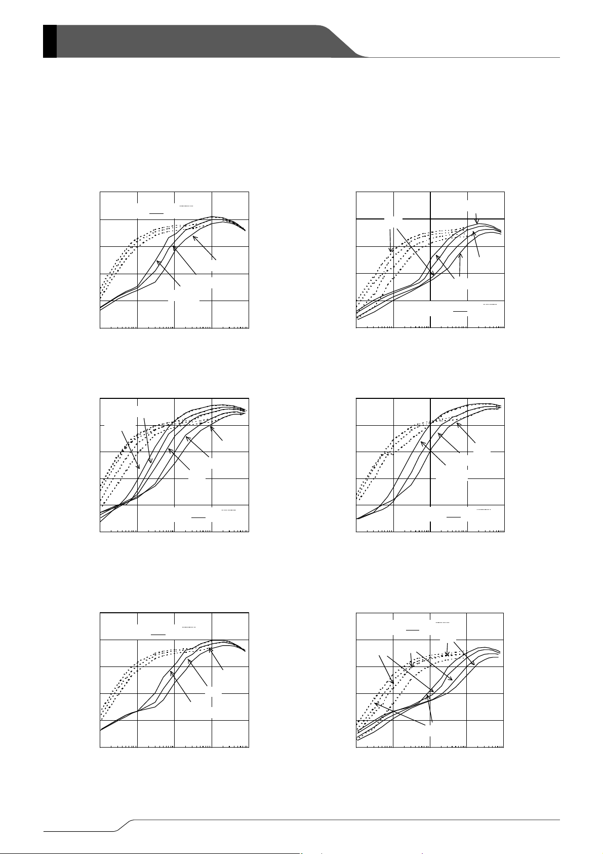
(1) Output Voltage vs. Output Current
FOSC= 1 80kHz , V
L1=22μH(CD RH 5D28), CL1=94μF(Tantalum )
1.7
PWM/PFM Switching Control
PWM Contr ol
1.6
(V)
OUT1
1.5
1.4
Output Voltage1 V
1.3
1.2
0.1 1 10 100 1000
Output Current 1 I
3.5
PWM/PFM Switching Control
PWM Contr ol
3.4
3.3
FOSC= 1 80kHz , V
L1=22μH(CD RH 5D28), CL1=94μF(Tantalum )
(V)
OUT1
3.2
Output Voltage1 V
3.1
= 1.5V
OUT1
SD1:C MS02, Tr1:XP161A1355P
VIN=0.9V
1.2V
(mA)
OUT1
= 3.3V
OUT1
SD1:C MS02, Tr1:XP161A1355P
2.7V
VIN=0.9V
1.2V,1.5V
FOSC= 1 80kHz , V
L1=22μH(CDRH5D28), CL1=94μF(Tantalum)
2.7
PWM/PFM Switching Control
PWM Contr ol
2.6
(V)
OUT1
2.5
2.4
Output Voltage1 V
2.3
2.2
0.1 1 10 100 1000
Output Current 1 I
FOSC= 1 80kHz , V
L1=22μH(CDRH5D28), CL1=94μF(Tantalum)
5.2
PWM/PFM Switching Control
PWM Contr ol
5.1
(V)
OUT1
5.0
4.9
Output Voltage1 V
4.8
= 2.5V
OUT1
SD1:C MS02, Tr1:XP161A1355P
1.5V
VIN=0.9V
(mA)
OUT1
= 5.0V
OUT1
SD1:C MS02, Tr1:XP161A1355P
VIN=1.5V
2.7V
1.2V
4.2V
3.3V
3.0
0.1 1 10 100 1000
Output Current 1 I
OUT1
(mA)
4.7
0.1 1 10 100 1000
Output Current 1 I
OUT1
(mA)
(V)
OUT1
Output Voltage1 V
FOSC=180kHz , V
8.2
PWM/PFM Switching Control
PWM Contr ol
8.1
8.0
7.9
7.8
= 8.0V
OUT1
L1=22μH(CDRH5D28), CL1=94μF(Tantalum)
SD1:C MS02, Tr1:XP161A1265P
5.0V
VIN=3.3V
4.2V
7.7
0.1 1 10 100 1000
Output Current 1 I
OUT1
(mA)
Dotted Arrowhead
PWM/PFM Switching Control
12/43

■TYPICAL PERFORMANCE CHARACTERISTICS (Continued)
< 1ch Step-Up DC/DC Controller >
(1) Output Voltage vs. Output Current (Continued)
(V)
OUT1
Output Voltage1 V
2.7
PWM/PFM Switching Control
PWM Contr ol
2.6
2.5
2.4
2.3
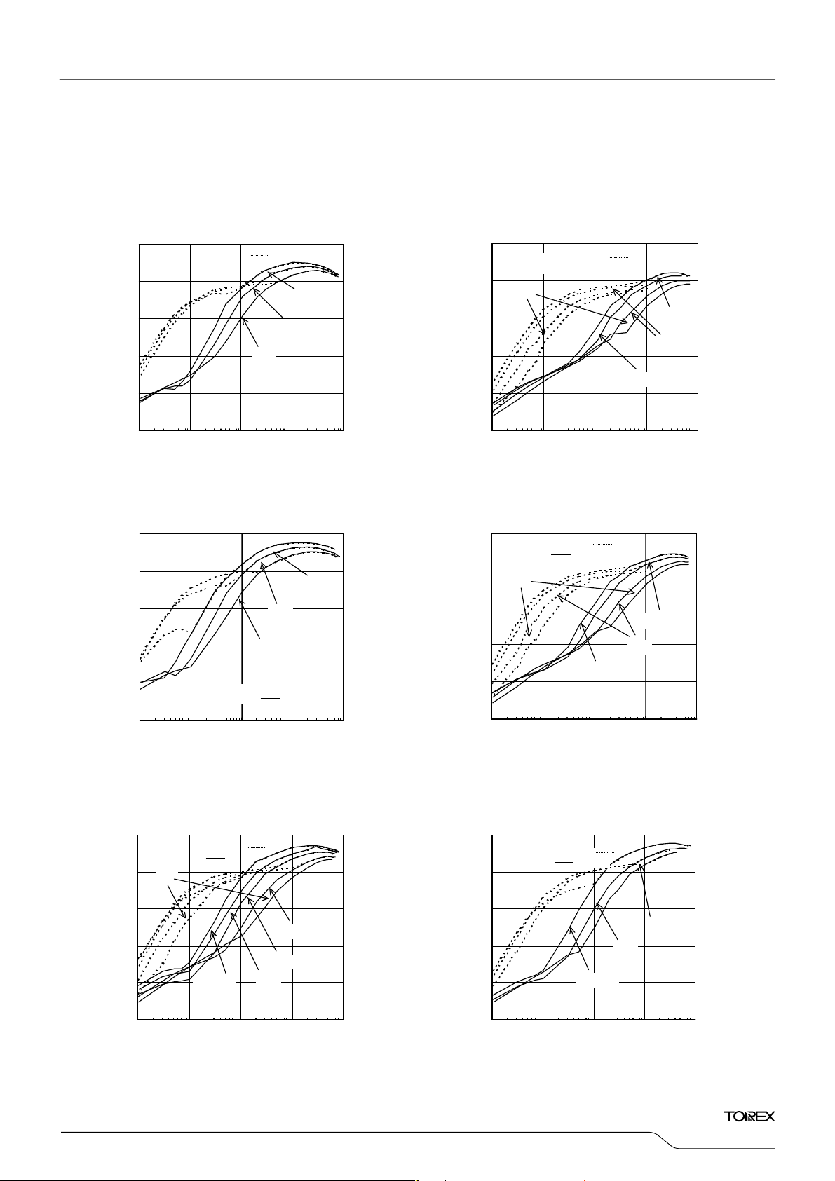
FOSC= 3 00kHz , V
L1=15μH(CDRH5D28), CL1=94μF(Tantalum)
= 2.5V
OUT1
SD1:C MS02, Tr1:XP161A1355P
VIN=0.9V
1.5V
1.2V
(V)
OUT1
Output Voltage1 V
3.5
PWM/PFM Switching Control
PWM Contr ol
3.4
3.3
3.2
3.1
FOSC= 3 00kHz , V
L1=15μH(CD RH 5D28), CL1=94μF(Tantalum)
= 3.3V
OUT1
SD1:C MS02, Tr1:XP161A1355P
VIN=0.9V
1.2V
XC9502
Series
2.7V
1.5V
2.2
0.1 1 10 100 1000
Output Current 1 I
FOSC= 3 00kHz , V
L1=15μH(CD RH 5D28), CL1=94μF(Tantalum)
5.2
PWM/PFM Switching Control
PWM Contr ol
5.1
(V)
OUT1
5.0
4.9
Output Voltage1 V
4.8
4.7
0.1 1 10 100 1000
Output Current 1 I
FOSC= 5 00kHz , V
L1=10μH(CDRH5D28), CL1=94μF(Tantalum)
3.5
PWM/PFM Switching Control
PWM Contr ol
3.4
(V)
OUT1
3.3
(mA)
OUT1
= 5.0V
OUT1
SD1:C MS02, Tr1:XP161A1355P
3.3V
VIN=1.2V
1.5V
(mA)
OUT1
= 3.3V
OUT1
SD1:C MS02, Tr1:XP161A1355P
1.5V
2.7V
2.7V
4.2V
3.0
0.1 1 10 100 1000
Output Current 1 I
FOSC= 5 00kHz , V
L1=10μH(CD RH 5D28), CL1=94μF(Tantalum)
2.7
PWM/PFM Switching Control
PWM Contr ol
2.6
(V)
OUT1
2.5
2.4
Output Voltage1 V
2.3
2.2
0.1 1 10 100 1000
Output Current 1 I
FOSC= 5 00kHz , V
L1=10μH(CD RH 5D28), CL1=94μF(Tantalum )
5.2
PWM/PFM Switching Control
PWM Contr ol
5.1
(V)
OUT1
5.0
(mA)
OUT1
= 2.5V
OUT1
SD1:C MS02, Tr1:XP161A1355P
1.5V
VIN=0.9V
1.2V
(mA)
OUT1
= 5.0V
OUT1
SD1:C MS02, Tr1:XP161A1355P
4.2V
3.3V
3.2
Output Voltage1 V
3.1
3.0
0.1 1 10 100 1000
Output Current 1 I
VIN=0.9V
OUT1
1.2V
(mA)
4.9
Output Voltage1 V
4.8
4.7
0.1 1 10 100 1000
Dotted Arrowhead
VIN=0.9V
Output Current 1 I
OUT1
1.2V
1.5V
(mA)
PWM/PFM Switching Control
2.7V
13/43

XC9502 Series
■TYPICAL PERFORMANCE CHARACTERISTICS (Continued)
< 1ch Step-Up DC/DC Controller >
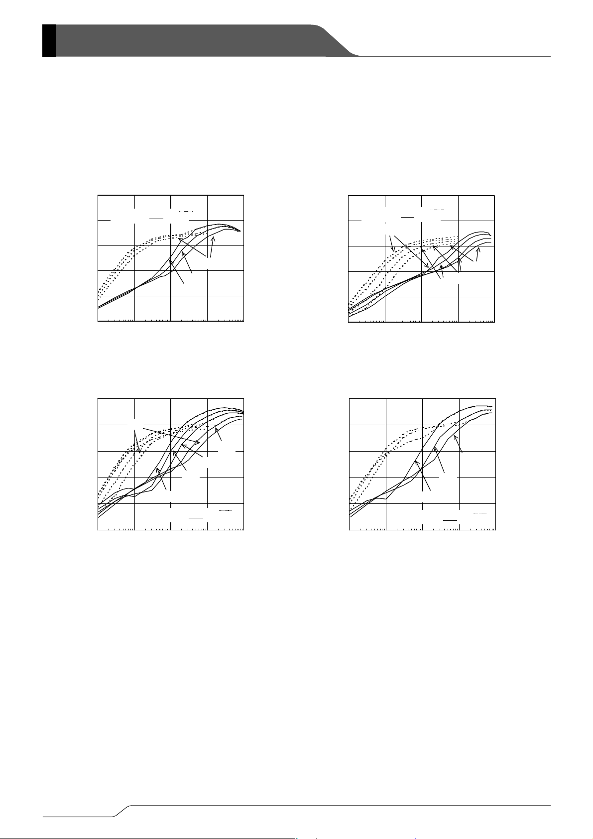
(2) Efficiency vs. Output Current
14/43
Dotted Arrowhead
PWM/PFM Switching Control

■TYPICAL PERFORMANCE CHARACTERISTICS (Continued)
< 1ch Step-Up DC/DC Controller >
(2) Efficiency vs. Output Current (Continued)
100
FOSC= 3 00kHz , V
L1=15μH(CDRH5D28), CL1=94μF(Tantalum)
= 2.5V
OUT1
SD1:C MS02, Tr1:XP161A1355P
80
100
80
FOSC= 3 00kHz , V
L1=15μH(CD RH 5D28), CL1=94μF(Tantalum)
= 3.3V
OUT1
SD1:C MS02, Tr1:XP161A1355P
2.7V
(%)
60
FFI 1
40
Efficiency1 E
20
0
0.1 1 10 100 1000
Output Current 1 I
FOSC= 3 00kHz , V
L1=15μH(CDRH5D28), CL1=94μF(Tantalum )
100
80
(%)
60
FFI 1
40
Efficiency1 E
20
0
0.1 1 10 100 1000
Output Current 1 I
VIN=0.9V
PWM/PFM Switching Control
PWM Contr ol
OUT1
= 5.0V
OUT1
SD1:C MS02, Tr1:XP161A1355P
VIN=1.2V
PWM/PFM Switching Control
PWM Contr ol
OUT1
1.5V
1.2V
(mA)
4.2V
3.3V
2.7V
1.5V
(mA)
(%)
60
FFI 1
40
Efficiency1 E
20
0
0.1 1 10 100 1000
PWM/PFM Switching Control
PWM Contr ol
Output Current 1 I
FOSC= 5 00kHz , V
L1=10μH(CD RH 5D28), CL1=94μF(Tantalum )
100
PWM/PF M Switching Control
PWM Contr ol
80
(%)
60
FFI 1
40
Efficiency1 E
20
0
0.1 1 10 100 1000
Output Current 1 I
1.2V
VIN=0.9V
(mA)
OUT1
= 2.5V
OUT1
SD1:C MS02, Tr1:XP161A1355P
VIN=0.9V
(mA)
OUT1
(%)
FFI 1
Efficiency1 E
100
PWM/PFM Switching Control
PWM Contr ol
80
60
40
20
FOSC= 5 00kHz , V
L1=10μH(CDRH5D28), CL1=94μF(Tantalum)
= 3.3V
OUT1
SD1:C MS02, Tr1:XP161A1355P
VIN=0.9
1.2V
2.7V
1.5V
(%)
FFI 1
Efficiency1 E
0
0.1 1 10 100 1000
Output Current 1 I
OUT1
(mA)
FOSC= 5 00kHz , V
L1=10μH(CDRH5D28), CL1=94μF(Tantalum)
100
4.2V
80
60
40
20
0
0.1 1 10 100 1000
Output Current 1 I
= 5.0V
OUT1
SD1:C MS02, Tr1:XP161A1355P
1.2V
VIN=0.9V
PWM/PFM Switching Control
PWM Contr ol
(mA)
OUT1
Dotted Arrowhead
PWM/PFM Switching Control
XC9502
Series
1.5V
1.5V
1.2V
3.3V
2.7V
1.5V
15/43

(
)
XC9502 Series
■TYPICAL PERFORMANCE CHARACTERISTICS
< 1ch Step-Up DC/DC Controller >
(3) Ripple Voltage vs. Output Current
Ripple Voltage1 (mV)
100
PWM/PFM Switching Control
PWM Contr ol
80
60
40
20
FOSC= 1 80kHz , V
L1=22μH(CD RH 5D28), CL1=94μF(Tantalum )
= 1.5V
OUT1
SD1:C MS02, Tr1:XP161A1355P
VIN=0.9V
1.2V
Ripple Voltage1 (mV)
0
0.1 1 10 100 1000
100
PWM/PFM Switching Control
PWM Contr ol
80
Output Current 1 I
FOSC= 1 80kHz , V
L1=22μH(CD RH 5D28), CL1=94μF(Tantalum )
(mA)
OUT1
= 3.3V
OUT1
SD1:C MS02, Tr1:XP161A1355P
60
VIN=0.9V
40
Ripple Voltage1 (mV)
20
0
0.1 1 10 100 1000
Output Current 1 I
2.7V
OUT1
1.5V
(mA)
Ripple Voltage1 (mV)
1.2
Ripple Voltage1 (mV)
100
PWM/PFM Switching Control
PWM Contr ol
80
60
40
20
FOSC= 1 80kHz , V
L1=22μH(CD RH 5D28), CL1=94μF(Tantalum )
= 8.0V
OUT1
SD1:C MS02, Tr1:XP161A1265P
VIN=3.3
V
4.2V
5.0V
0
0.1 1 10 100 1000
Output Current 1 I
OUT1
(mA)
Dotted Arrowhead
FOSC= 1 80kHz , V
100
PWM/PFM Switching Control
PWM Contr ol
80
VIN=0.9V
1.2V
1.5V
60
40
20
0
0.1 1 10 100 1000
FOSC= 1 80kHz , V
100
PWM/PFM Switching Control
PWM Contr ol
80
60
40
20
0
0.1 1 10 100 1000
Continued
= 2.5V
OUT1
L1=22μH(CD RH 5D28), CL1=94μF(Tantalum )
Output Current 1 I
L1=22μH(CDRH5D28), CL1=94μF(Tantalum)
Output Current 1 I
SD1:C MS02, Tr1:XP161A1355P
OUT1
= 5.0V
OUT1
SD1:C MS02, Tr1:XP161A1355P
VIN=1.5V
OUT1
(mA)
4.2V
2.7V
3.3V
(mA)
PWM/PFM Switching Control
16/43

■TYPICAL PERFORMANCE CHARACTERISTICS (Continued)
< 1ch Step-Up DC/DC Controller >
(3) Ripple Voltage vs. Output Current (Continued)
100
PWM/PFM Switching Control
PWM Contr ol
80
60
40
20
FOSC= 3 00kHz , V
L1=15μH(CD RH 5D28), CL1=94μF(Tantalum )
Ripple Voltage1 (mV)
100
PWM/PFM Switching Control
PWM Contr ol
80
60
40
20
FOSC= 3 00kHz , V
L1=15μH(CD RH 5D28), CL1=94μF(Tantalum)
= 2.5V
OUT1
SD1:C MS02, Tr1:XP161A1355P
1.2V
VIN=0.9V
1.5V
Ripple Voltage1 (mV)
= 3.3V
OUT1
SD1:C MS02, Tr1:XP161A1355P
1.2V
VIN=0.9V
2.7V
0
0.1 1 10 100 1000
(mA)
OUT1
= 5.0V
OUT1
SD1:C MS02, Tr1:XP161A1355P
4.2V
3.3V
2.7V
1.5V
VIN=1.2V
100
PWM/PFM Switching Control
PWM Contr ol
80
60
Output Current 1 I
FOSC= 3 00kHz , V
L1=15μH(CD RH 5D28), CL1=94μF(Tantalum )
0
0.1 1 10 100 1000
(mA)
OUT1
= 2.5V
OUT1
SD1:C MS02, Tr1:XP161A1355P
VIN=0.9V
100
80
60
Output Current 1 I
FOSC= 5 00kHz , V
L1=10μH(CD RH 5D28), CL1=94μF(Tantalum )
PWM/PF M Switching Control
PWM Contr ol
40
Ripple Voltage1 (mV)
20
40
Ripple Voltage1 (mV)
20
0
0.1 1 10 100 1000
Output Current 1 I
OUT1
(mA)
0
0.1 1 10 100 1000
Output Current 1 I
OUT1
(mA)
Ripple Voltage1 (mV)
100
PWM/PFM Switching Control
PWM Contr ol
80
60
40
20
FOSC= 5 00kHz , V
L1=10μH(CD RH 5D28), CL1=94μF(Tantalum)
= 3.3V
OUT1
SD1:C MS02, Tr1:XP161A1355P
1.2V
VIN=0.9V
2.7V
1.5V
100
80
60
40
Ripple Voltage1 (mV)
20
FOSC= 5 00kHz , V
L1=10μH(CDRH5D28), CL1=94μF(Tantalum)
PWM/PFM Switching Control
PWM Contr ol
OUT1
SD1:C MS02, Tr1:XP161A1355P
1.2V
VIN=0.9V
= 5.0V
2.7V
1.5V
0
0.1 1 10 100 1000
Output Current 1 I
OUT1
(mA)
0
0.1 1 10 100 1000
Output Current 1 I
OUT1
(mA)
Dotted Arrowhead PWM/PFM Switching Control
XC9502
Series
1.5V
1.2V
1.5V
4.2V
3.3V
17/43

XC9502 Series
■TYPICAL PERFORMANCE CHARACTERISTICS (Continued)
< 2ch Step-Down DC/DC Controller >
(4) Output Voltage vs. Output Current
18/43
FOSC=180kHz , V
L2=47μH(CD RH 6D38), CL2=94μF(Tantalum)
1.2
PWM C ontrol
1.1
(V)
OUT2
1.0
0.9
Output Voltage2 V
0.8
0.7
0.1 1 10 100 1000
Output Current2 I
FOSC=180kHz , V
L2=47μH(CDRH6D38), CL2=94μF(Tantalum)
3.5
PWM/PFM Switching Control
PWM Contr ol
3.4
(V)
OUT2
3.3
3.2
Output Voltage2 V
3.1
3.0
0.1 1 10 100 1000
VIN=4.2V 5.0V 6.0V 8.0V 10V
Output Current2 I
FOSC=300kHz , V
L2=22μH(CD RH 5D28), CL2=94μF(Tantalum )
1.2
PWM C ontrol
1.1
(V)
OUT2
1.0
0.9
Output Voltage2 V
0.8
0.7
0.1 1 10 100 1000
VIN=2.7V 3.3V 4.2V 5.0V
6.0V 8.0V 10V
Output Current2 I
=1.0V
OUT2
SD2:C MS02, Tr2:XP162A12A6P
10V
VIN=2.7V 3.3V 4.2V
5.0V 6.0V 8.0V
(mA)
OUT2
=3.3V
OUT2
SD2:C MS02, Tr2:XP162A12A6P
(mA)
OUT2
=1.0V
OUT2
SD2:C MS02, Tr2:XP162A12A6P
(mA)
OUT2
*When setting V
L should be 94μF (Tantalum) + 100μF (OS capacitor)
C
1.2
PWM/PFM Switching Control
1.1
(V)
OUT2
1.0
0.9
Output Voltage2 V
0.8
0.7
0.1 1 10 100 1000
5.2
PWM/PFM Switching Control
PWM Contr ol
5.1
(V)
OUT2
5.0
4.9
Output Voltage2 V
4.8
4.7
0.1 1 10 100 1000
1.2
PWM/PFM Switching Control
1.1
(V)
OUT2
1.0
0.9
Output Voltage2 V
0.8
0.7
0.1 1 10 100 1000
OUT = 1.0V, VIN = 8.0V, 10.0V
FOSC=180kHz , V
L2=47μH(CDRH6D38), CL2=94μF(Tantalum)
4.2V 5.0V 6.0V 8.0V
Output Current2 I
FOSC=180kHz , V
L2=47μH(CDRH6D38), CL2=94μF(Tantalum )
Output Current2 I
FOCS=300kHz , V
L2=22μH(CDRH5D28), CL2=94μF(Tantalum)
4.2V 6.0V 8.0V 10V
Output Current2 I
=1.0V
OUT2
SD2:C MS02, Tr2:XP162A12A6P
10V
VIN=2.7V 3.3V
(mA)
OUT2
=5.0V
OUT2
SD2:C MS02, Tr2:XP162A12A6P
VIN= 6.0V 8.0V 10V
(mA)
OUT2
=1.0V
OUT2
SD2:C MS02, Tr2:XP162A12A6P
VIN=2.7V 3.3V
5.0V
(mA)
OUT2
■
)
TYPICAL PERFORMANCE CHARACTERISTICS (Continued
< 2ch Step-Down DC/DC Controller >
(4) Output Voltage vs. Output Current (Continued)
(V)
OUT2
Output Voltage2 V
2.0
1.9
1.8
1.7
1.6
PWM C ontrol
FOSC=300kHz , V
L2=22μH(CDRH5D28), CL2=94μF(Tantalum)
VIN= 2.7V 3.3V 4.2V
5.0V 6.0V 8.0V 10V
=1.8V
OUT2
SD2:C MS02, Tr2:XP162A12A6P
2.0
PWM/PFM Switching Control
1.9
(V)
OUT2
1.8
1.7
Output Voltage2 V
1.6
FOSC=300kHz , V
L2=22μH(CDRH5D28), CL2=94μF(Tantalum)
VIN= 2.7V 3.3V 4.2V 5.0V
1.5
0.1 1 10 100 1000
Output Current2 I
FOSC=300kHz , V
L2=22μH(CD RH 5D28), CL2=94μF(Tantalum)
2.7
PWM Contr ol
2.6
(V)
OUT2
2.5
(mA)
OUT2
=2.5V
OUT2
SD2:C MS02, Tr2:XP162A12A6P
10.0V
1.5
0.1 1 10 100 1000
Output Current2 I
FOSC=300kHz , V
L2=22μH(CDRH5D28), CL2=94μF(Tantalum)
2.7
PWM/PFM Switching Control
2.6
(V)
OUT2
2.5
2.4
VIN= 2.7V 3.3V 4.2V
Output Voltage2 V
2.3
5.0V 6.0V 8.0V
2.4
Output Voltage2 V
2.3
3.3V 4.2V 5.0V 6.0V
2.2
0.1 1 10 100 1000
Output Current2 I
OUT2
(mA)
2.2
0.1 1 10 100 1000
Output Current2 I
(V)
OUT2
Output Voltage2 V
FOSC=300kHz , V
L2=22μH(CD RH 5D28), CL2=94μF(Tantalum )
3.5
PWM Contr ol
3.4
3.3
3.2
3.1
3.0
0.1 1 10 100 1000
VIN=4.2V 5.0V 6.0V 8.0V
Output Current2 I
=3.3V
OUT2
SD2:C MS02, Tr2:XP162A12A6P
10.0V
(mA)
OUT2
FOSC=300kHz , V
L2=22μH(CDRH5D28), CL2=94μF(Tantalum)
3.5
PWM/PFM Switching Control
3.4
(V)
OUT2
3.3
3.2
Output Voltage2 V
3.1
3.0
0.1 1 10 100 1000
VIN=4.2V 5.0V 6.0V 8.0V
Output Current2 I
=1.8V
OUT2
SD2:C MS02, Tr2:XP162A12A6P
6.0V 8.0V 10V
(mA)
OUT2
=2.5V
OUT2
SD2:C MS02, Tr2:XP162A12A6P
10V
8.0V
VIN=2.7V
(mA)
OUT2
=3.3V
OUT2
SD2:C MS02, Tr2:XP162A12A6P
10.0V
(mA)
OUT2
XC9502
Series
19/43
XC9502 Series
■TYPICAL PERFORMANCE CHARACTERISTICS (Continued)
< 2ch Step-Down DC/DC Controller >
(4) Output Voltage vs. Output Current (Continued)
(V)
OUT2
Output Voltage2 V
(V)
OUT2
Output Voltage2 V
(V)
OUT2
Output Voltage2 V
FOSC=300kHz , V
L2=22μH(CDRH5D28), CL2=94μF(Tantalum)
5.2
PWM Contr ol
5.1
5.0
4.9
4.8
4.7
0.1 1 10 100 1000
Output Current2 I
FOSC=500kHz , V
L2=10μH(CDRH5D28), CL2=94μF(Tantalum)
1.2
PWM C ontrol
1.1
1.0
0.9
0.8
0.7
0.1 1 10 100 1000
VIN=2.7V 3.3V 4.2V 5.0V
Output Current2 I
FOSC=500kHz , V
L2=10μH(CD RH 5D28), CL2=94μF(Tantalum)
3.5
PWM Contr ol
3.4
3.3
VIN=4.2V 5.0V 6.0V 8.0V 10V
3.2
3.1
3.0
0.1 1 10 100 1000
Output Current2 I
=5.0V
OUT2
SD2:C MS02, Tr2:XP162A12A6P
10.0V
VIN= 6.0V 8.0V
(mA)
OUT2
=1.0V
OUT2
SD2:C MS02, Tr2:XP162A12A6P
6.0V 8.0V 10V
(mA)
OUT2
=3.3V
OUT2
SD2:C MS02, Tr2:XP162A12A6P
(mA)
OUT2
FOSC=300kHz , V
L2=22μH(CDRH5D28), CL2=94μF(Tantalum)
5.2
PWM/PFM Switching Control
5.1
(V)
OUT2
5.0
4.9
Output Voltage2 V
4.8
4.7
0.1 1 10 100 1000
Output Current2 I
FOSC=500kHz , V
L2=10μH(CD RH 5D28), CL2=94μF(Tantalum)
1.2
PWM/PF M Switching Control
1.1
(V)
OUT2
1.0
0.9
Output Voltage2 V
0.8
0.7
0.1 1 10 100 1000
VIN=2.7V 3.3V 4.2V 5.0V
6.0V 8.0V 10V
Output Current2 I
FOSC=500kHz , V
L2=10μH(CDRH5D28), CL2=94μF(Tantalum)
3.5
PWM/PFM Switching Control
3.4
(V)
OUT2
3.3
VIN=4.2V 5.0V 6.0V 8.0V
3.2
Output Voltage2 V
3.1
3.0
0.1 1 10 100 1000
Output Current2 I
=5.0V
OUT2
SD2:C MS02, Tr2:XP162A12A6P
10.0V
VIN= 6.0V 8.0V
(mA)
OUT2
=1.0V
OUT2
SD2:C MS02, Tr2:XP162A12A6P
(mA)
OUT2
=3.3V
OUT2
SD2:C MS02, Tr2:XP162A12A6P
10V
(mA)
OUT2
20/43
*When setting VOUT = 1.0V, VIN = 8.0V, 10.0V
C
L should be 94μF (Tantalum) + 100μF (OS capacitor)
■TYPICAL PERFORMANCE CHARACTERISTICS (Continued)
< 2ch Step-Down DC/DC Controller >
(4) Output Voltage vs. Output Current (Continued)
(V)
OUT2
FOSC=300kHz , V
5.2
PWM/PFM Switching Control
PWM Contr ol
5.1
5.0
4.9
=5.0V
OUT2
L2=10μH(CDRH5D28), CL2=94μF(Tantalum)
SD2:C MS02, Tr2:XP162A12A6P
VIN= 6.0V 8.0V 10V
Output Voltage2 V
4.8
4.7
0.1 1 10 100 1000
Output Current2 I
OUT2
(mA)
*When setting V
C
L should be 94μF (Tantalum) + 100μF (OS capacitor)
OUT = 1.0V, VIN = 8.0V, 10.0V
XC9502
Series
21/43
(
)
XC9502 Series
■TYPICAL PERFORMANCE CHARACTERISTICS
< 2ch Step-Down DC/DC Controller >
(5) Efficiency vs. Output Current
100
(%)
FFI12
Efficiency2 E
100
(%)
FFI12
Efficiency2 E
100
(%)
FFI12
Efficiency2 E
FOSC=180kHz , V
L2=47μH(CDRH6D28), CL2=94μF(Tantalum)
PWM/PF M Switching Control
PWM Contr ol
80
60
40
20
0
0.1 1 10 100 1000
Output Current2 I
FOSC=180kHz , V
L2=47μH(CD RH 6D28), CL2=94μF(Tantalum)
5.0V
80
VIN=4.2V
60
40
20
0
0.1 1 10 100 1000
PWM/PFM Switching Control
PWM Contr ol
Output Current2 I
FOSC=300kHz , V
L2=22μH(CDRH5D28), CL2=94μF(Tantalum)
PWM/PFM Switching Control
PWM Contr ol
80
60
40
20
0
0.1 1 10 100 1000
Output Current2 I
=1.0V
OUT2
SD2:C MS02, Tr2:XP162A12A6P
4.2V
3.3V
VIN=2.7V
(mA)
OUT2
=3.3V
OUT2
SD2:C MS02, Tr2:XP162A12A6P
10V
8.0V
6.0V
(mA)
OUT2
=1.0V
OUT2
SD2:C MS02, Tr2:XP162A12A6P
4.2V
3.3V
VIN=2.7V
(mA)
OUT2
*When setting VOUT = 1.0V, VIN = 8.0V, 10.0V
C
L should be 94μF (Tantalum) + 100μF (OS capacitor)
FOSC=180kHz , V
100
80
(%)
60
FFI12
40
Efficiency2 E
20
0
0.1 1 10 100 1000
FOSC=180kHz , V
100
80
(%)
60
FFI12
40
Efficiency2 E
20
0
0.1 1 10 100 1000
FOSC=300kHz , V
100
PWM/PF M Switching Control
PWM Contr ol
80
(%)
FFI12
Efficiency2 E
6.0V
60
40
20
0
0.1 1 10 100 1000
Continued
=1.0V
OUT2
L2=47μH(CDRH6D28), CL2=94μF(Tantalum)
8.0V
Output Current2 I
L2=47μH(CD RH 6D28), CL2=94μF(Tantalum)
Output Current2 I
L2=22μH(CD RH 5D28), CL2=94μF(Tantalum)
Output Current2 I
SD2:C MS02, Tr2:XP162A12A6P
PWM/PF M Switching Control
PWM Contr ol
OUT2
=5.0V
OUT2
SD2:C MS02, Tr2:XP162A12A6P
VIN=6.0V
PWM/PFM Switc hing Control
PWM Control
OUT2
=1.0V
OUT2
SD2:C MS02, Tr2:XP162A12A6P
8.0V
10V
VIN=5.0V
OUT2
VIN=5.0V
6.0V
10V
(mA)
10V
8.0V
(mA)
(mA)
22/43
■TYPICAL PERFORMANCE CHARACTERISTICS (Continued)
< 2ch Step-Down DC/DC Controller >
(5) Efficiency vs. Output Current (Continued)
100
80
60
40
20
FOSC=300kHz , V
L2=22μH(CD RH 5D28), CL2=94μF(Tantalum)
PWM/PFM Switc hing Control
PWM Control
10V
(%)
FFI12
Efficiency2 E
100
80
60
40
20
FOSC= 3 00kHz , V
L2=22μH(CD RH 5D28), CL2=94μF(Tantalum)
PWM/PF M Switching Control
PWM Contr ol
=1.8V
OUT2
SD2:C MS02, Tr2:XP162A12A6P
4.2V
VIN= 2.7V
3.3V
(%)
FFI12
Efficiency2 E
=1.8V
OUT2
SD2:C MS02, Tr2:XP162A12A6P
0
0.1 1 10 100 1000
Output Current2 I
OUT2
(mA)
100
FOSC=300kHz , V
L2=22μH(CD RH 5D28), CL2=94μF(Tantalum)
=2.5V
OUT2
SD2:C MS02, Tr:2XP162A12A6P
80
(%)
60
FFI12
VIN=2.7V
3.3V
0
0.1 1 10 100 1000
Output Current2 I
FOSC=300kHz , V
L2=22μH(CD RH 5D28), CL2=94μF(Tantalum )
100
PWM/PFM Switching Control
PWM Contr ol
80
10V
(%)
60
FFI12
(mA)
OUT2
=2.5V
OUT2
SD2:C MS02, Tr2:XP162A12A6P
40
Efficiency2 E
20
0
0.1 1 10 100 1000
PWM/PFM Switching Control
PWM Contr ol
Output Current2 I
4.2V
OUT2
(mA)
40
Efficiency2 E
20
0
0.1 1 10 100 1000
Output Current2 I
6.0V
OUT2
8.0V
(mA)
(%)
FFI12
Efficiency2 E
100
80
60
40
20
FOSC=300kHz , V
L2=22μH(CDRH5D28), CL2=94μF(Tantalum)
PWM/PF M Switching Control
PWM Contr ol
10V
VIN=4.2V
=3.3V
OUT2
SD2:C MS02, Tr2:XP162A12A6P
5.0V
6.0V
8.0V
100
80
(%)
60
FFI12
40
Efficiency2 E
20
FOSC=300kHz , V
L2=22μH(CDRH5D28), CL2=94μF(Tantalum )
PWM/PFM Switching Control
PWM Contr ol
OUT2
SD2:C MS02, Tr2:XP162A12A6P
8.0V
VIN=6.0V
=5.0V
0
0.1 1 10 100 1000
Output Current2 I
OUT2
(mA)
*When setting VOUT = 1.0V, VIN = 8.0V, 10.0V
C
L should be 94μF (Tantalum) + 100μF (OS capacitor)
0
0.1 1 10 100 1000
Output Current2 I
OUT2
(mA)
XC9502
Series
VIN=5.0V
8.0V
6.0V
VIN=5.0V
10V
23/43
XC9502 Series
■TYPICAL PERFORMANCE CHARACTERISTICS (Continued)
< 2ch Step-Down DC/DC Controller >
(5) Efficiency vs. Output Current (Continued)
(%)
FFI12
Efficiency2 E
(%)
FFI12
Efficienc y2 E
FOSC=500kHz , V
L2=10μH(CD RH 5D28), CL2=94μF(Tantalum )
100
PWM/PFM Switching Control
PWM Contr ol
80
60
40
20
0
0.1 1 10 100 1000
Output Current2 I
FOSC=500kHz , V
L2=10μH(CDRH5D28), CL2=94μF(Tantalum)
100
80
60
40
20
0
0.1 1 10 100 1000
10V
VIN=4.2V
PWM/PF M Switching Control
PWM Contr ol
Output Current2 I
=1.0V
OUT2
SD2:C MS02, Tr2:XP162A12A6P
4.2V
3.3V
VIN=2.7V
(mA)
OUT2
=3.3V
OUT2
SD2:C MS02, Tr2:XP162A12A6P
8.0V
6.0V
5.0V
(mA)
OUT2
*When setting VOUT = 1.0V, VIN = 8.0V, 10.0V
C
L should be 94μF (Tantalum) + 100μF (OS capacitor)
FOSC=500kHz , V
L2=10μH(CDRH5D28), CL2=94μF(Tantalum)
100
PWM/PFM Switching Control
PWM Contr ol
80
(%)
60
FFI12
40
Efficiency2 E
20
0
0.1 1 10 100 1000
VIN=5.0V
Output Current2 I
FOSC=500kHz , V
L2=10μH(CD RH 5D28), CL2=94μF(Tantalum)
100
80
(%)
60
FFI12
40
Efficienc y2 E
20
0
0.1 1 10 100 1000
PWM/PFM Switching Control
PWM Contr ol
Output Current2 I
=1.0V
OUT2
SD2:C MS02, Tr2:XP162A12A6P
6.0V
(mA)
OUT2
=3.3V
OUT2
SD2:C MS02, Tr2:XP162A12A6P
8.0V
VIN=6.0V
(mA)
OUT2
10V
8.0V
10V
24/43
■TYPICAL PERFORMANCE CHARACTERISTICS (Continued)
< 2ch Step-Down DC/DC Controller >
(6) Ripple Voltage vs. Output Current
Ripple Voltage2 (mV)
100
80
60
40
20
FOSC=180kHz , V
L2=47μH(CDRH6D28), CL2=94μF(Tantalum)
PWM Contr ol
OUT2
SD2:C MS02, Tr2:XP162A12A6P
VIN=2.7V 3.3V 4.2V 5.0V
6.0V 8.0V 10V
=1.0V
100
80
60
40
Ripple Voltage2 (mV)
20
FOSC=180kHz , V
L2=47μH(CD RH 6D28), CL2=94μF(Tantalum)
PWM/PF M Switching Control
VIN=2.7V
OUT2
SD2CMS02, Tr2:XP162A12A6P
5.0V4.2V
=1.0V
6.0V10V
0
0.1 1 10 100 1000
Output Current2 I
OUT2
(mA)
0
0.1 1 10 100 1000
Output Current2 I
OUT2
(mA)
100
80
FOSC=180kHz , V
L2=47μH(CDRH6D28), CL2=94μF(Tantalum)
PWM Contr ol
=3.3V
OUT2
SD2:C MS02, Tr2:XP162A12A6P
100
PWM/PFM Switching Control
80
FOSC=180kHz , V
L2=47μH(CDRH6D28), CL2=94μF(Tantalum)
=3.3V
OUT2
SD2:C MS02, Tr2:XP162A12A6P
60
40
Ripple Voltage2 (mV)
20
VIN=4.2V 6.0V
5.0V
10V
8.0V
60
VIN=4.2V
40
Ripple Voltage2 (mV)
20
5.0V
10V
8.0V6.0V
0
0.1 1 10 100 1000
Output Current2 I
OUT2
(mA)
0
0.1 1 10 100 1000
Output Current2 I
OUT2
(mA)
100
80
FOSC=180kHz , V
L2=47μH(CDRH6D28), CL2=94μF(Tantalum)
PWM Contr ol
OUT2
SD2:C MS02, Tr2:XP162A12A6P
=5.0V
100
PWM/PFM Switching Control
80
FOSC=180kHz , V
L2=47μH(CD RH 6D28), CL2=94μF(Tantalum )
=5.0V
OUT2
SD2:C MS02, Tr2:XP162A12A6P
60
60
40
Ripple Voltage2 (mV)
20
VIN=6.0V
10V
8.0V
40
Ripple Voltage2 (mV)
20
8.0V
0
0.1 1 10 100 1000
Output Current2 I
OUT2
(mA)
*When setting V
C
L should be 94μF (Tantalum) + 100μF (OS capacitor)
OUT = 1.0V, VIN = 8.0V, 10.0V
0
0.1 1 10 100 1000
Output Current2 I
OUT2
(mA)
XC9502
Series
8.0V
3.3V
10VVIN=6.0V
25/43

XC9502 Series
■TYPICAL PERFORMANCE CHARACTERISTICS (Continued)
< 2ch Step-Down DC/DC Controller >
(6) Ripple Voltage vs. Output Current (Continued)
Ripple Voltage2 (mV)
Ripple Voltage2 (mV)
Ripple Voltage2 (mV)
FOSC=300kHz , V
L2=22μH(CD RH 5D28), CL2=94μF(Tantalum)
100
PWM Contr ol
80
60
40
20
0
0.1 1 10 100 1000
VIN=2.7V 3.3V 5.0V 6.0V
Output Current2 I
FOSC=300kHz , V
L2=22μH(CD RH 5D28), CL2=94μF(Tantalum )
100
PWM Contr ol
80
VIN=2.7V 3.3V 4.2V 5.0V
60
40
20
0
0.1 1 10 100 1000
6.0V 8.0V 10V
Output Current2 I
FOSC=300kHz , V
L2=22μH(CDRH5D28), CL2=94μF(Tantalum)
100
PWM Contr ol
80
VIN=2.7V 3.3V 4.2V 5.0V
60
40
20
0
0.1 1 10 100 1000
Output Current2 I
=1.0V
OUT2
SD2:C MS02, Tr2:XP162A12A6P
8.0V 10V
4.2V
(mA)
OUT2
=1.8V
OUT2
SD2:C MS02, Tr2:XP162A12A6P
(mA)
OUT2
=2.5V
OUT2
SD2:C MS02, Tr2:XP162A12A6P
6.0V 8.0V 10V
(mA)
OUT2
*When setting VOUT = 1.0V, VIN = 8.0V, 10.0V
C
L should be 94μF (Tantalum) + 100μF (OS capacitor)
FOSC=300kHz , V
L2=22μH(CD RH 5D28), CL2=94μF(Tantalum)
100
PWM/PFM Switching Control
80
60
6.0V
5.0V
Output Current2 I
40
Ripple Voltage2 (mV)
20
0
0.1 1 10 100 1000
FOSC=300kHz , V
L2=22μH(CD RH 5D28), CL2=94μF(Tantalum)
100
PWM/PFM Switching Control
80
60
5.0V
10V
40
Ripple Voltage2 (mV)
20
0
0.1 1 10 100 1000
6.0V
8.0V
Output Current2 I
FOSC=300kHz , V
L2=22μH(CDRH5D28), CL2=94μF(Tantalum)
100
PWM/PFM Switching Control
80
60
10V
40
Ripple Voltage2 (mV)
20
0
0.1 1 10 100 1000
5.0V
Output Current2 I
=1.0V
OUT2
SD2:C MS02, Tr2:XP162A12A6P
VIN=2.7V
8.0V
OUT2
4.2V
OUT2
4.2V6.0V8.0V
OUT2
OUT2
OUT2
3.3V
(mA)
=1.8V
3.3V
(mA)
=2.5V
3.3V
(mA)
4.2V10V
SD2:C MS02, Tr2:XP162A12A6P
SD2:C MS02, Tr2:XP162A12A6P
VIN=2.7V
VIN=2.7V
26/43

■TYPICAL PERFORMANCE CHARACTERISTICS (Continued)
< 2ch Step-Down DC/DC Controller >
(6) Ripple Voltage vs. Output Current (Continued)
Ripple Voltage2 (mV)
100
80
60
40
20
FOSC=300kHz , V
L2=22μH(CDRH5D28), CL2=94μF(Tantalum)
PWM Contr ol
OUT2
SD2:C MS02, Tr2:XP162A12A6P
VIN=4.2V 5.0V 6.0V
8.0V 10V
=3.3V
100
80
60
40
Ripple Volt age 2 ( mV)
20
FOSC=300kHz , V
L2=22μH(CDRH5D28), CL2=94μF(Tantalum)
PWM/PFM Switching Control
VIN=4.2V
OUT2
SD2:C MS02, Tr2:XP162A12A6P
8.0V6.0V5.0V
=3.3V
10.0V
0
0.1 1 10 100 1000
Output Current2 I
OUT2
(mA)
0
0.1 1 10 100 1000
Output Current2 I
OUT2
(mA)
FOSC=300kHz , V
L2=22μH(CDRH5D28), CL2=94μF(Tantalum)
100
PWM Contr ol
80
=5.0V
OUT2
SD2:C MS02, Tr2:XP162A12A6P
100
PWM/PFM Switching Control
80
FOSC=300kHz , V
L2=22μH(CDRH5D28), CL2=94μF(Tantalum)
=5.0V
OUT2
SD2:C MS02, Tr2:XP162A12A6P
60
OUT2
VIN=6.0V
8.0V
(mA)
40
Ripple Voltage2 (mV)
20
0
0.1 1 10 100 1000
Output Current2 I
10V
60
40
Ripple Voltage2 (mV)
20
0
0.1 1 10 100 1000
8.0V
Output Current2 I
10.0VVIN=6.0V
(mA)
OUT2
FOSC=500kHz , V
L2=10μH(CD RH 5D28), CL2=94μF(Tantalum )
100
PWM Contr ol
80
=1.0V
OUT2
SD2:C MS02, Tr2:XP162A12A6P
100
PWM/PFM Switching Control
80
FOSC=500kHz , V
L2=10μH(CD RH 5D28), CL2=94μF(Tantalum)
=1.0V
OUT2
SD2:C MS02, Tr2:XP162A12A6P
60
40
Ripple Voltage2 (mV)
20
0
0.1 1 10 100 1000
VIN=2.7V 3.3V 4.2V 5.0V
6.0V 8.0V 10V
Output Current2 I
OUT2
*When setting VOUT = 1.0V, VIN = 8.0V, 10.0V
C
60
VIN=2.7V
40
Ripple Voltage2 (mV)
20
0
0.1 1 10 100 1000
(mA)
Output Current2 I
L should be 94μF (Tantalum) + 100μF (OS capacitor)
OUT2
4.2V6.0V
(mA)
5.0V10V8.0V
XC9502
Series
3.3V
27/43

XC9502 Series
■TYPICAL PERFORMANCE CHARACTERISTICS (Continued)
< 2ch Step-Down DC/DC Controller >
(6) Ripple Voltage vs. Output Current (Continued)
100
PWM Contr ol
80
FOSC=500kHz , V
L2=10μH(CDRH5D28), CL2=94μF(Tantalum)
=3.3V
OUT2
SD2:C MS02, Tr2:XP162A12A6P
60
10V
8.0V
5.0V
6.0V
Ripple Voltage2 (mV)
40
Ripple Voltage2 (mV)
20
VIN=4.2V
0
0.1 1 10 100 1000
Output Current2 I
FOSC=500kHz , V
L2=10μH(CD RH 5D28), CL2=94μF(Tantalum)
100
PWM Contr ol
80
(mA)
OUT2
=5.0V
OUT2
SD2:C MS02, Tr2:XP162A12A6P
60
8.0V
10V
Ripple Voltage2 (mV)
40
Ripple Voltage2 (mV)
20
VIN=6.0V
0
0.1 1 10 100 1000
Output Current2 I
OUT2
(mA)
*When setting VOUT = 1.0V, VIN = 8.0V, 10.0V
L should be 94μF (Tantalum) + 100μF (OS capacitor)
C
FOSC=500kHz , V
L2=10μH(CD RH 5D28), CL2=94μF(Tantalum)
100
PWM/PFM Switching Control
80
60
VIN=4.2V
5.0V
40
20
0
0.1 1 10 100 1000
6.0V
Output Current2 I
FOSC=500kHz , V
L2=10μH(CDRH5D28), CL2=94μF(Tantalum)
100
PWM/PFM Switching Control
80
60
40
VIN=6.0V
20
0
0.1 1 10 100 1000
8.0V
Output Current2 I
=3.3V
OUT2
SD2:C MS02, Tr2:XP162A12A6P
8.0V
(mA)
OUT2
=5.0V
OUT2
SD2:C MS02, Tr2:XP162A12A6P
10V
(mA)
OUT2
10V
28/43

■TYPICAL PERFORMANCE CHARACTERISTICS (Continued)
(7) Supply Current vs. Supply Voltage
(9) Supply Current 1-2 vs. Supply Voltage
(11) Supply Current 1-4 vs. Supply Voltage
(8) Supply Current 1-1 vs. Supply Voltage
(10) Supply Current 1-3 vs. Supply Voltage
(12) Supply Current 2 vs. Supply Voltage
XC9502
Series
29/43

XC9502 Series
■TYPICAL PERFORMANCE CHARACTERISTICS (Continued)
(13) Oscillation Frequency vs. Supply Voltage
(15) PWM1, 2 'H' 'L' Voltage vs. Supply Voltage
(17) Maximum Duty Ratio 1 vs. Supply Voltage (18) PFM Duty Ratio 1, 2 vs. Supply Voltage
30/43
(14) Stand-by Current vs. Supply Voltage
(16) EN1, 2 'H' 'L' Voltage vs. Supply Voltage

■TYPICAL PERFORMANCE CHARACTERISTICS (Continued)
(19) EXT 1, 2 High ON Resistance vs. Supply Voltage
(21) Output Voltage vs. Ambient Temperature
(23) Operation Retention Voltage vs. Ambient Temperature
(20) EXT 1, 2 Low ON Resistance vs. Supply Voltage
(22) Oscillation Start-Up Voltage vs. Ambient Temperature
(24) Operation Start-Up Voltage vs. Ambient Temperature
XC9502
Series
31/43

XC9502 Series
■TYPICAL PERFORMANCE CHARACTERISTICS (Continued)
(25) Soft-Start Time 1, 2 vs. Supply Voltage
32/43
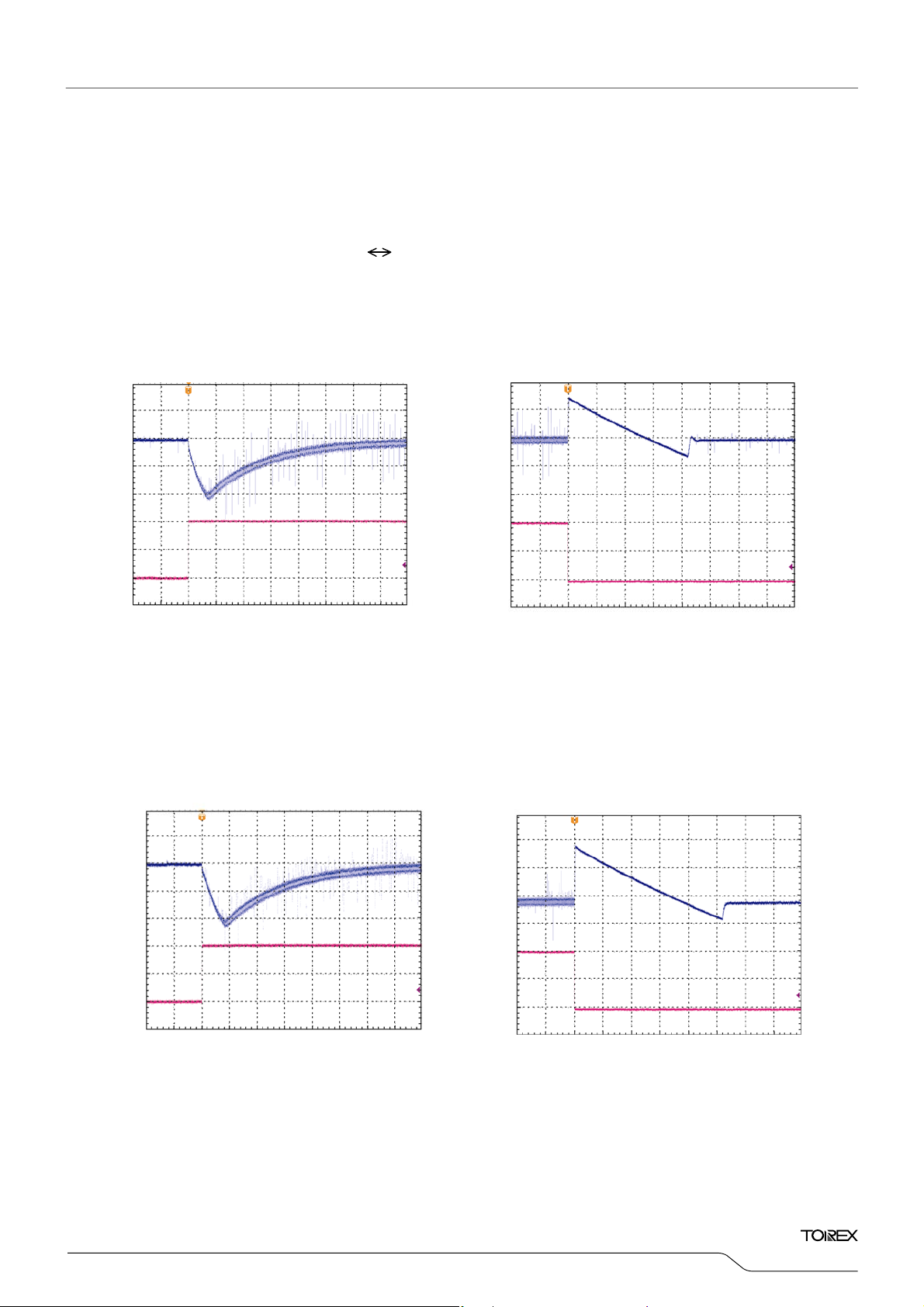
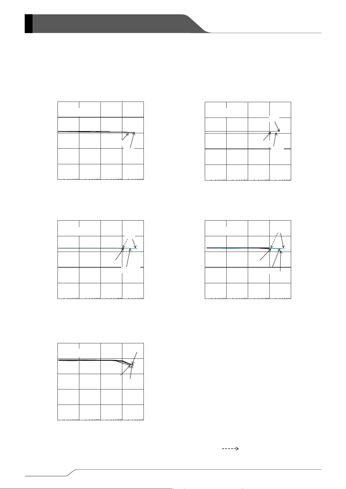
■TYPICAL PERFORMANCE CHARACTERISTICS (Continued)
(26) Load Transient Response
[1 channel: Step-Up DC/DC Controller]
OUT1 = 3.3V, VIN = 2.0V, IOUT1, 2 =100μA 100mA >
< V
● PWM Control
CH1
CH2
FOSC=180kHz, V
IN=2.0V, IOUT1=100μA→100mA
V
OUT1=3.3V
200μsec/div
CH1: V
OUT1, AC-COUPLED, 50mV/div
OUT1, 50mA/div
CH2: I
● PWM/PFM Switching Control
OUT1=3.3V
CH1
CH2
FOSC=180kHz, V
IN=2.0V, IOUT1=100μA→100mA
V
200μsec/div
CH1: VOUT1, AC-COUPLED, 50mV/div
OUT1, 50mA/div
CH2: I
3.3V
100mA
100μA
3.3V
100mA
100μA
CH1
CH2
CH1
CH2
FOSC=180kHz, VOUT1=3.3V
IN=2.0V, IOUT1=100mA→100μA
V
10msec/div
CH1: VOUT1, AC-COUPLED, 50mV/div
OUT1, 50mA/div
CH2: I
FOSC=180kHz, V
IN=2.0V, IOUT1=100mA→100μA
V
OUT1=3.3V
10msec/div
CH1: VOUT1, AC-COUPLED, 50mV/div
OUT1, 50mA/div
CH2: I
XC9502
Series
3.3V
100mA
100μA
3.3V
100mA
100μA
33/43
XC9502 Series
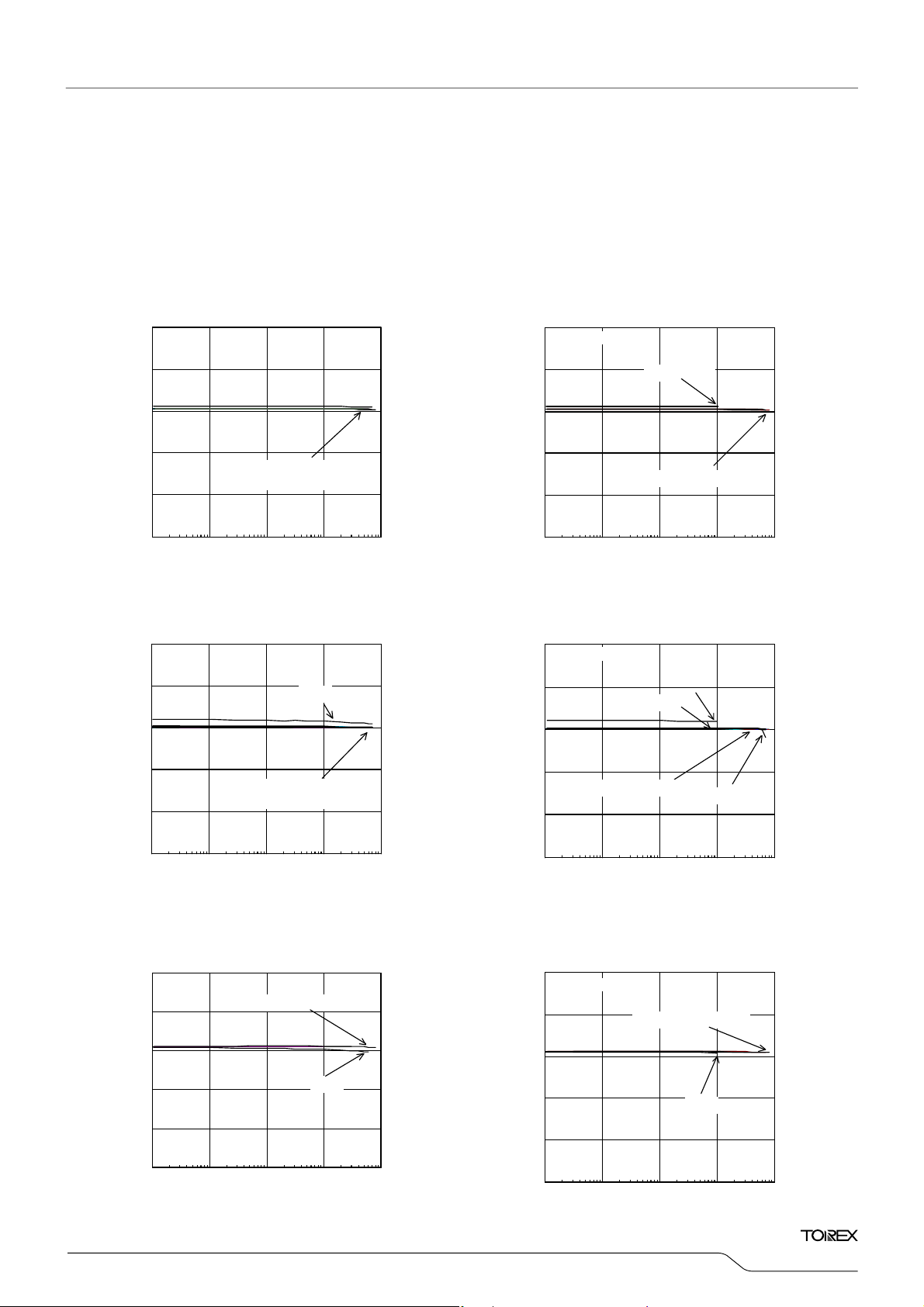
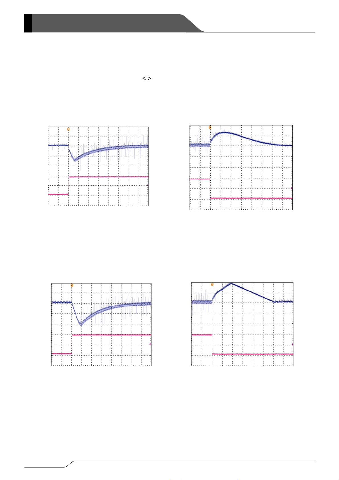
■TYPICAL PERFORMANCE CHARACTERISTICS (Continued)
(26) Load Transient Response (Continued)
< VOUT1 = 3.3V, VIN = 2.0V, IOUT1, 2 =10mA 100mA >
● PWM Control
OUT1=3.3V
CH1
CH2
FOSC=180kHz, V
IN=2.0V, IOUT1=10mA→100mA
V
200μsec/div
OUT1, AC-COUPLED, 50mV/div
CH1: V
OUT1, 50mA/div
CH2: I
● PWM/PFM Switching Control
CH1
CH2
FOSC=180kHz, V
IN=2.0V, IOUT1=10mA→100mA
V
OUT1=3.3V
200μsec/div
CH1: VOUT1, AC-COUPLED, 50mV/div
OUT1, 50mA/div
CH2: I
3.3V
100mA
10mA
3.3V
100mA
10mA
CH1
CH2
CH1
CH2
FOSC=180kHz, V
IN=2.0V, IOUT1=100mA→10mA
V
200μsec/div
CH1: V
OUT1, AC-COUPLED, 50mV/div
OUT1, 50mA/div
CH2: I
FOSC=180kHz, V
IN=2.0V, IOUT1=100mA→10mA
V
200μsec/div
CH1: V
OUT1, AC-COUPLED, 50mV/div
OUT1, 50mA/div
CH2: I
OUT1=3.3V
OUT1=3.3V
3.3V
100mA
10mA
3.3V
100mA
10mA
34/43
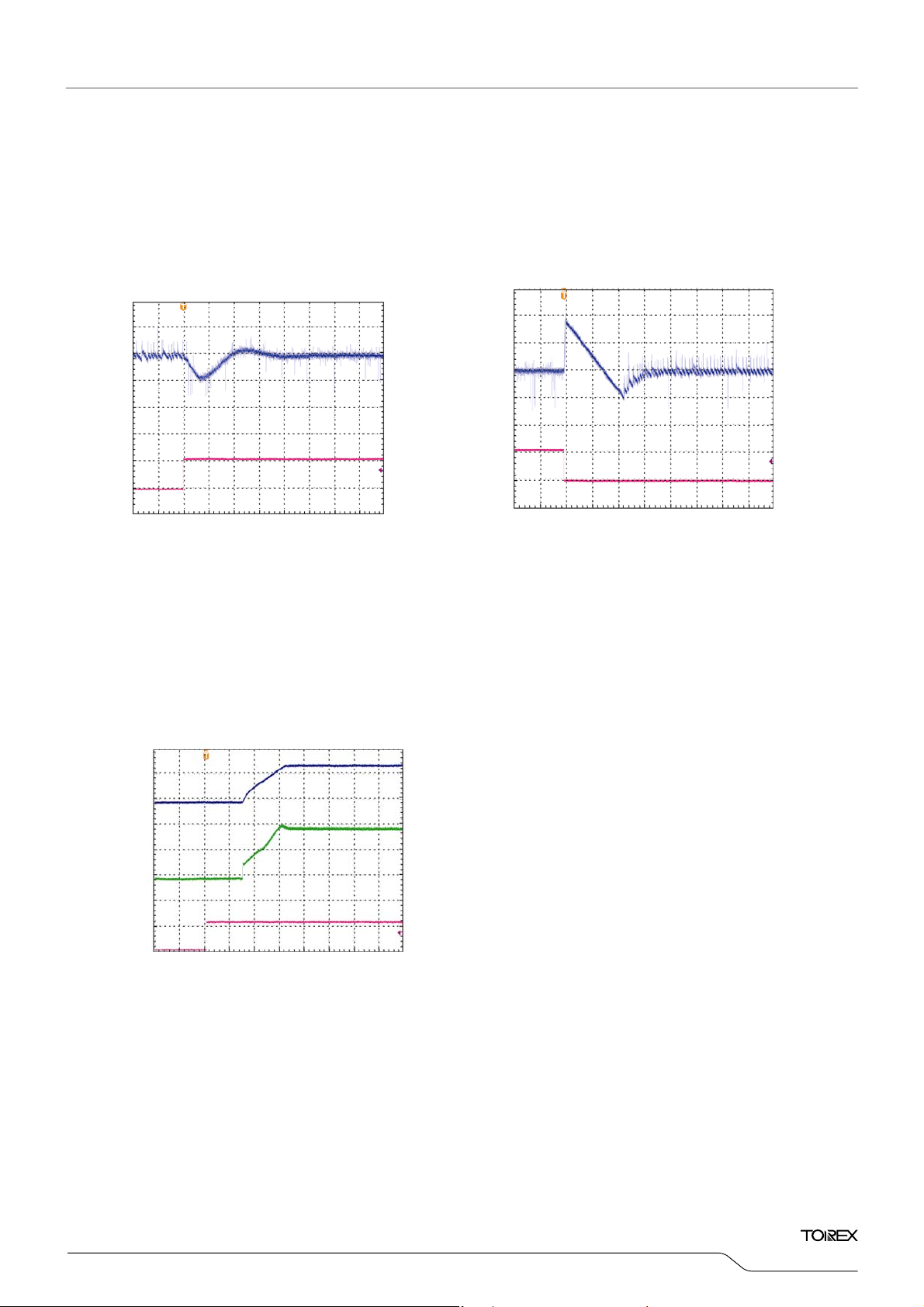
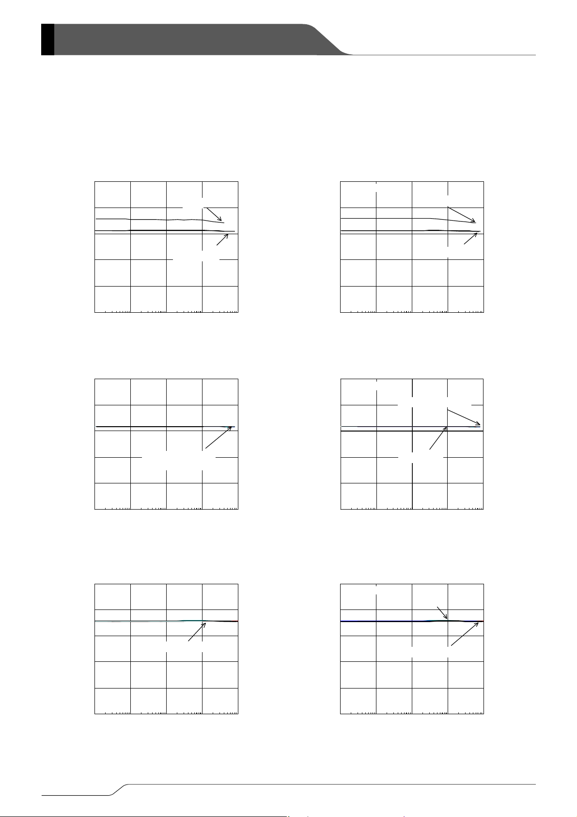
■TYPICAL PERFORMANCE CHARACTERISTICS (Continued)
(26) Load Transient Response (Continued)
<PWM Control→PWM/PFM Switching Control>
CH1
CH2
FOSC=180kHz, V
IN=2.0V, IOUT1=1mA, PWM1 ’L’→’H’
V
OUT1=3.3V
1msec/div
CH1: VOUT1, AC-COUPLED, 10mV/div
CH2: PWM1, 0.5V/div
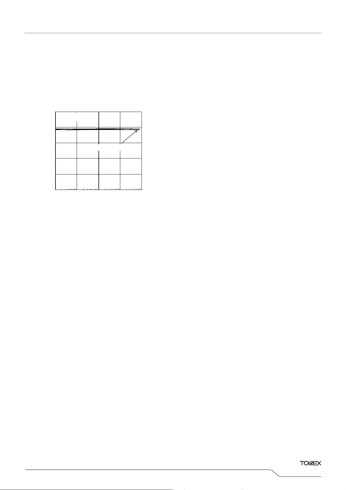
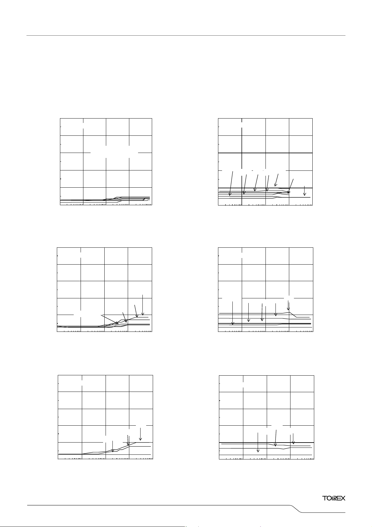
<Soft Start Wave Form>
CH1
CH2
CH3
FOSC=180kHz, V
V
IN=2.0V, IOUT1=100mA, EN1 ’L’→’H’
C
OUT1=3.3V
IN=47μF
4ms/div
CH1: VOUT1, 1.0V/div
CH2: I
IN1, 100mA/div
CH3: EN1, 0.5V/div
3.3V
0.65V
0V
3.3V
300mA
0.65V
CH1
CH2
* EN2=GND
FOSC=180kHz, V
IN=2.0V, IOUT1=1mA, PWM1 ’H’→’L’
V
OUT1=3.3V
1msec/div
CH1: VOUT1, AC-COUPLED, 10mV/div
CH2: PWM1, 0.5V/div
XC9502
Series
3.3V
0.65V
0V
35/43
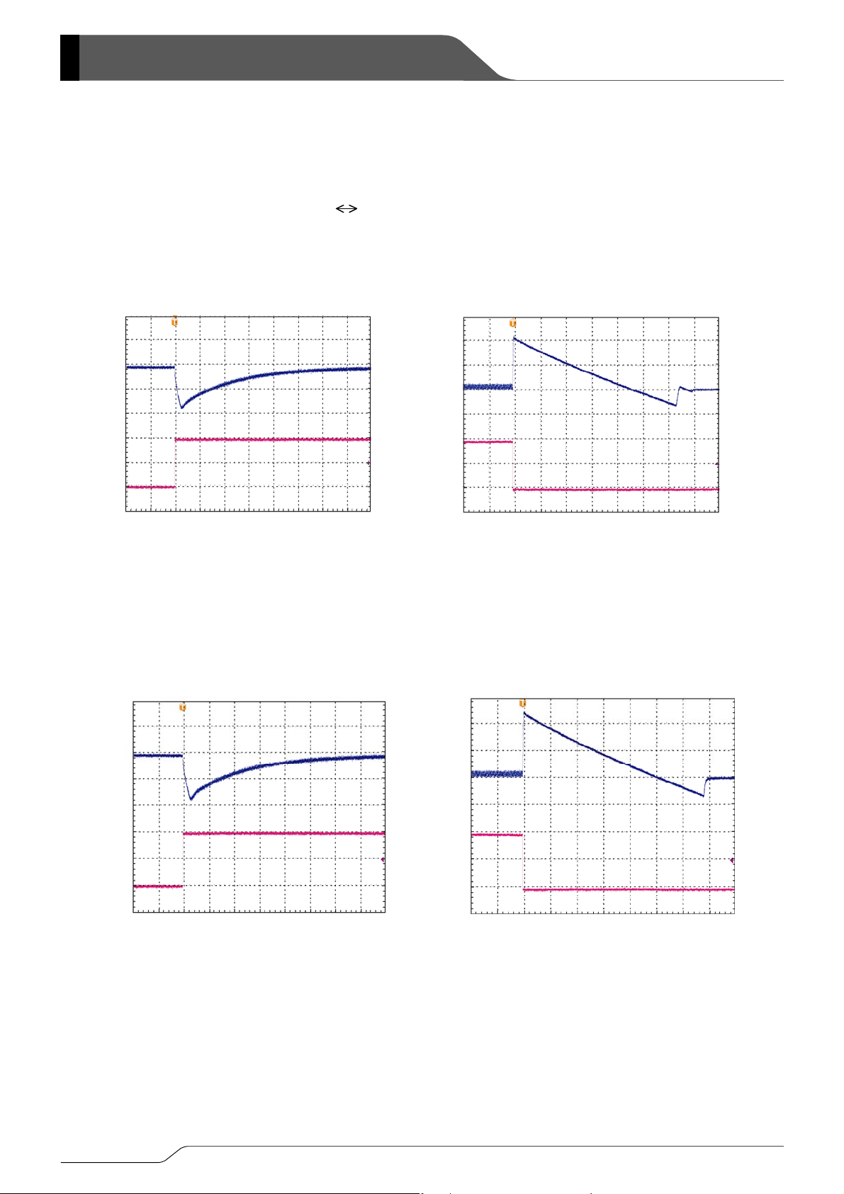
(
)
XC9502 Series
■TYPICAL PERFORMANCE CHARACTERISTICS
(26) Load Transient Response (Continued)
< VOUT2=3.3V, VIN=5.0V, IOUT2=100μA 300mA>
● PWM Control
CH1
CH2
FOSC=300kHz, V
IN=5.0V, IOUT2=100μA→ 300mA
V
OUT2=3.3V
200μsec/div
CH1: V
OUT2, AC-COUPLED, 100mV/div
OUT2, 150mA/div
CH2: I
● PWM/PFM Switching Control
FOSC=300kHz, VOUT2=3.3V
IN=5.0V, IOUT2=100μA→ 300mA
V
CH1
CH2
200μsec/div
CH1: VOUT2, AC-COUPLED, 100mV/div
OUT2, 150mA/div
CH2: I
3.3V
300mA
100μA
3.3V
300mA
100μA
FOSC=300kHz, V
IN=5.0V, IOUT2=300mA→100μA
V
CH1
CH2
CH1: V
OUT2, 150mA/div
CH2: I
FOSC=300kHz, V
V
CH1
CH2
IN=5.0V, IOUT2=300mA→100μA
CH1: VOUT2, AC-COUPLED, 100mV/div
OUT2, 150mA/div
CH2: I
Continued
OUT2=3.3V
10msec/div
OUT2, AC-COUPLED, 50mV/div
OUT2=3.3V
10msec/div
3.3V
300mA
100μA
3.3V
300mA
100μA
36/43
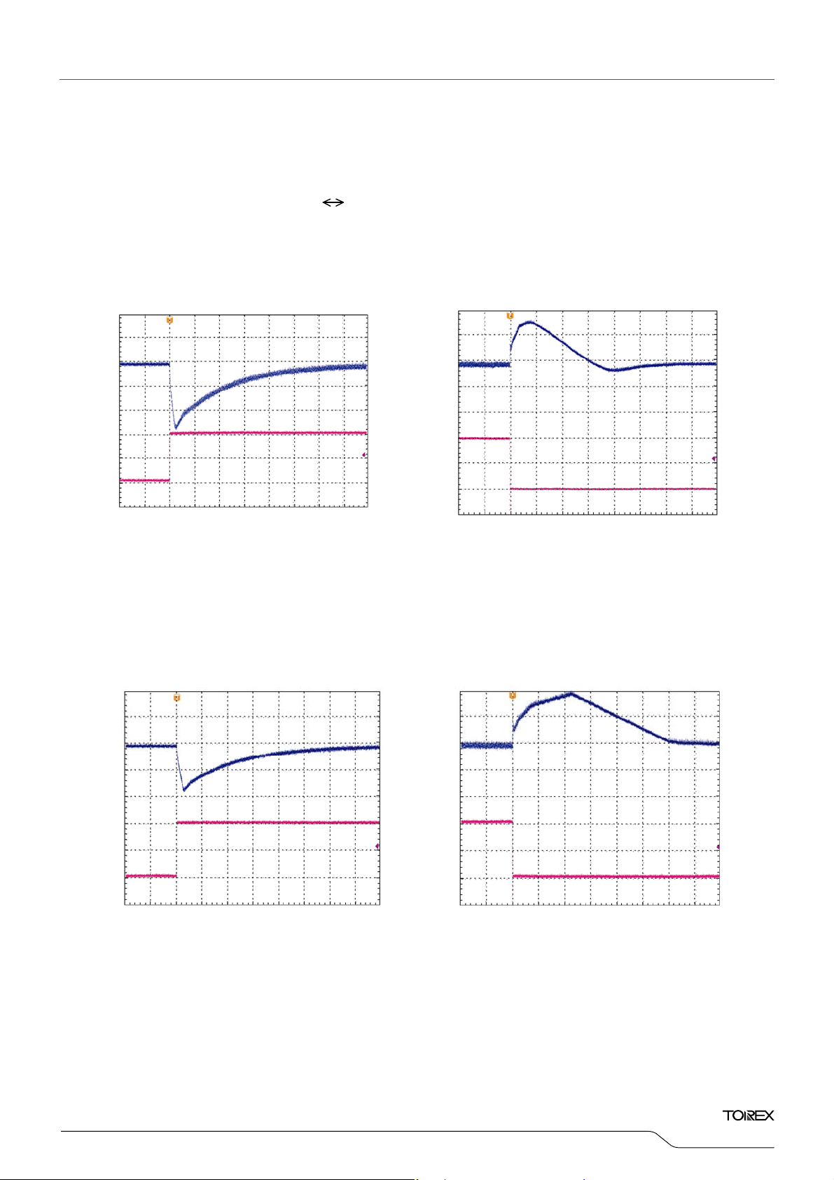
■TYPICAL PERFORMANCE CHARACTERISTICS (Continued)
(26) Load Transient Response (Continued)
< VOUT2=3.3V, VIN=5.0V, IOUT2=10mA 300mA>
● PWM Control
OUT2=3.3V
CH1
CH2
FOSC=300kHz, V
IN=5.0V, IOUT2=10mA→ 300mA
V
200μsec/div
CH1: V
OUT2, AC-COUPLED, 50mV/div
OUT2, 150mA/div
CH2: I
● PWM/PFM Switching Control
OUT2=3.3V
CH1
CH2
FOSC=300kHz, V
IN=5.0V, IOUT2=10mA→ 300mA
V
200μsec/div
CH1: VOUT2, AC-COUPLED, 100mV/div
OUT2, 150mA/div
CH2: I
3.3V
300mA
10mA
3.3V
300mA
10mA
CH1
CH2
CH1
CH2
FOSC=300kHz, V
IN=5.0V, IOUT2=300mA→10mA
V
OUT2=3.3V
400μsec/div
CH1: VOUT2, AC-COUPLED, 50mV/div
OUT2, 150mA/div
CH2: I
FOSC=300kHz, VOUT2=3.3V
IN=5.0V, IOUT2=300mA→10mA
V
200μsec/div
CH1: VOUT2, AC-COUPLED, 50mV/div
OUT2, 150mA/div
CH2: I
XC9502
Series
3.3V
300mA
10mA
3.3V
300mA
10mA
37/43
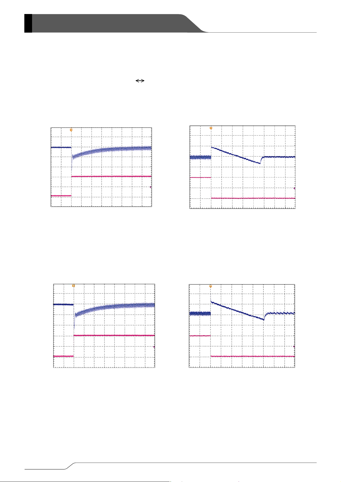
XC9502 Series
■TYPICAL PERFORMANCE CHARACTERISTICS (Continued)
(26) Load Transient Response (Continued)
< VOUT2=0.9V, VIN=3.3V, IOUT2=100μA 300mA>
● PWM Control
CH1
CH2
FOSC=300kHz, V
IN=3.3V, IOUT2=100μA→ 300mA
V
OUT2=0.9V
200μsec/div
CH1: VOUT2, AC-COUPLED, 20mV/div
OUT2, 150mA/div
CH2: I
● PWM/PFM Switching Control
CH1
CH2
FOSC=300kHz, V
IN=3.3V, IOUT2=100μA→ 300mA
V
OUT2=0.9V
200μsec/div
CH1: VOUT2, AC-COUPLED, 20mV/div
OUT2, 150mA/div
CH2: I
0.9V
300mA
μA
100
0.9V
300mA
100
μA
FOSC=300kHz, V
IN=3.3V, IOUT2=300mA→100μA
V
CH1
CH2
4msec/div
CH1: VOUT2, AC-COUPLED, 20mV/di
CH2: IOUT2, 150mA/div
FOSC=300kHz, V
IN=3.3V, IOUT2=300mA→100μA
V
CH1
CH2
4msec/div
CH1: VOUT2, AC-COUPLED, 20mV/div
OUT2, 150mA/div
CH2: I
OUT2=0.9V
OUT2=0.9V
0.9V
300mA
μA
100
0.9V
300mA
μA
100
38/43

■TYPICAL PERFORMANCE CHARACTERISTICS (Continued)
(26) Load Transient Response (Continued)
< VOUT2=0.9V, VIN=3.3V, IOUT2=10mA 300mA>
● PWM Control
FOSC=300kHz, VOUT2=0.9V
IN=3.3V, IOUT2=10mA→ 300mA
V
CH1
CH2
100μsec/div
OUT2, AC-COUPLED, 20mV/div
CH1: V
OUT2, 150mA/div
CH2: I
● PWM/PFM Switching Control
FOSC=300kHz, VOUT2=0.9V
IN=3.3V, IOUT2=10mA→ 300mA
V
CH1
CH2
200μsec/div
CH1: VOUT2, AC-COUPLED, 20mV/div
OUT2, 150mA/div
CH2: I
0.9V
300mA
10mA
0.9V
300mA
10mA
CH1
CH2
CH1
CH2
FOSC=300kHz, VOUT2=0.9V
IN=3.3V, IOUT2=300mA→10mA
V
100μsec/div
CH1: V
OUT2, AC-COUPLED, 20mV/div
OUT2, 150mA/div
CH2: I
FOSC=300kHz, VOUT2=0.9V
IN=3.3V, IOUT2=300mA→10mA
V
200μsec/div
CH1: VOUT2, AC-COUPLED, 20mV/div
OUT2, 150mA/div
CH2: I
XC9502
Series
0.9V
300mA
10mA
0.9V
300mA
10mA
39/43
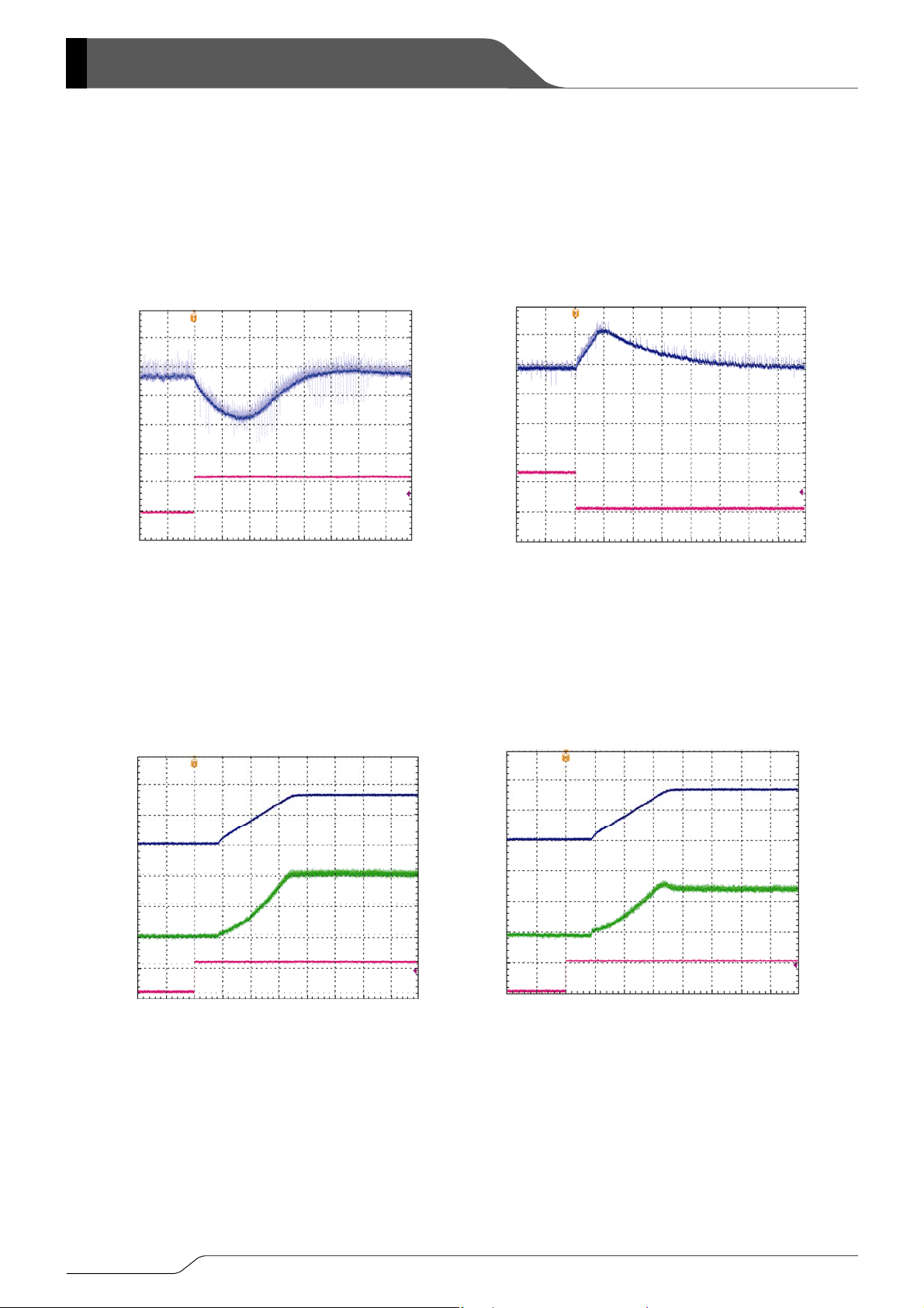
XC9502 Series
■TYPICAL PERFORMANCE CHARACTERISTICS (Continued)
(26) Load Transient Response (Continued)
40/43
<PWM Control ⇔ PWM/PFM Switching Control>
CH1
CH2
FOSC=300kHz, V
IN=5.0V, IOUT2=5mA, PWM2 ’L’→’H’
V
OUT2=3.3V
400μsec/div
CH1: VOUT2, AC-COUPLED, 10mV/div
CH2: PWM2, 0.5V/div
<Soft Start Wave Form>
OUT2=3.3V
CH1
CH2
CH3
FOSC=300kHz, V
V
IN=5.0V, IOUT2=300mA, EN2 ’L’→’H’
IN=47μF
C
4ms/div
CH1: VOUT2, 2.0V/div
CH2: I
IN2, 100mA/div
CH3: EN2, 0.5V/div
3.3V
0.65V
0V
3.3V
CH1
200mA
0.65V
CH2
* EN1=GND
IN=5.0V, IOUT2=5mA, PWM2 ’H’→’L’
V
CH1
CH2
CH1: V
CH2: PWM2, 0.5V/div
FOSC=300kHz, V
V
IN=5.0V, IOUT2=100mA, EN2 ’L’→’H’
FOSC=300kHz, V
OUT2=3.3V
200μsec/div
OUT2, AC-COUPLED, 20mV/div
OUT2=3.3V
IN=47μF
C
4ms/div
CH1: VOUT2, 2.0V/div
CH2: I
IN2, 50mA/div
CH3: EN2, 0.5V/div
3.3V
0.65V
0V
3.3V
75mA
0.65V

■
PACKAGING INFORMATION
●MSOP-10 ●USP-10
●USP-10 Recommended Pattern Layout ●USP-10 Recommended Metal Mask Design
2.3
XC9502
Series
41/43

■
XC9502 Series
MARKING RULE
●MSOP-10, USP-10
MSOP-10
(TOP VIEW)
USP-10
(TOP VIEW)
① represents product series
MARK PRODUCT SERIES
3 XC9502B09xxx
② represents type of DC/DC converter
MARK PRODUCT SERIES
B XC9502B09xxx
③, ④ represents FB voltage
MARK
③ ④
0 9 0.9 XC9502B09xxx
⑤ represents oscillation frequency
MARK
2 180 XC9502B092xx
3 300 XC9502B093xx
5 500 XC9502B095xx
OSCILLATION FREQUENCY
VOLTAGE
(kHz)
(V)
PRODUCT SERIES
PRODUCT SERIES
⑥ represents production lot number
0 to 9, A to Z repeated (G, I, J, O, Q, W excluded)
Note: No character inversion used.
42/43

XC9502
Series
1. The products and product specifications contained herein are subject to change without
notice to improve performance characteristics. Consult us, or our representatives
before use, to confirm that the information in this datasheet is up to date.
2. We assume no responsibility for any infringement of patents, patent rights, or other
rights arising from the use of any information and circuitry in this datasheet.
3. Please ensure suitable shipping controls (including fail-safe designs and aging
protection) are in force for equipment employing products listed in this datasheet.
4. The products in this datasheet are not developed, designed, or approved for use with
such equipment whose failure of malfunction can be reasonably expected to directly
endanger the life of, or cause significant injury to, the user.
(e.g. Atomic energy; aerospace; transport; combustion and associated safety
equipment thereof.)
5. Please use the products listed in this datasheet within the specified ranges.
Should you wish to use the products under conditions exceeding the specifications,
please consult us or our representatives.
6. We assume no responsibility for damage or loss due to abnormal use.
7. All rights reserved. No part of this datasheet may be copied or reproduced without the
prior permission of TOREX SEMICONDUCTOR LTD.
43/43
 Loading...