

TOREX XC9301, XC9302 User Manual
■
■
A
■
■
0
f
(%)
XC9301/XC9302 Series
ETR0601_001c
PWM,PWM/PFM Switching Step-Up & Down DC/DC Converter Controller ICs
GENERAL DESCRIPTIO N
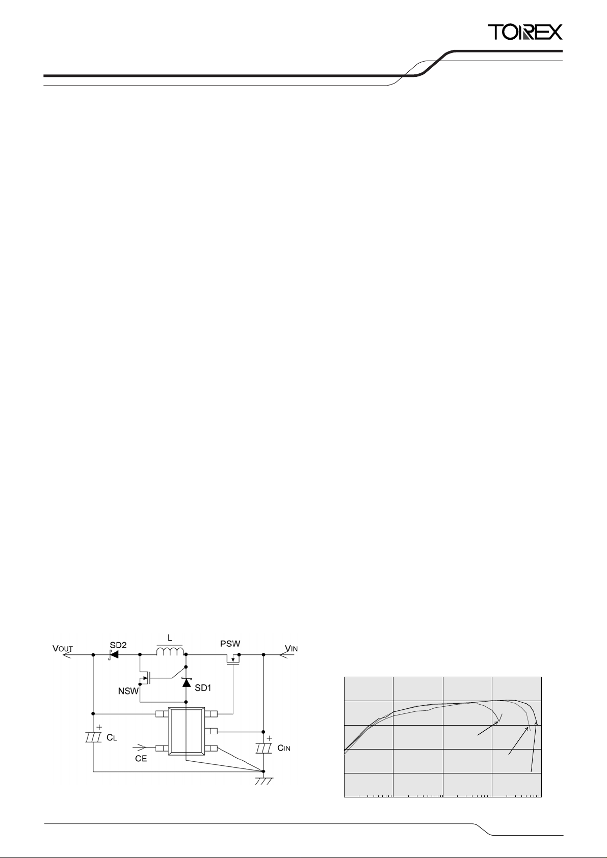
The XC9301/XC9302 series are step-up/down DC/DC conv erter controller ICs with fast, low ON resistance drivers built-in. A
versatile, large output current, step-up/down DC/DC converter can be realized using only 4 type of basic external components
two transistors, one inductor, two diodes and capacitors.
Output voltage is selectable in 0.1V increments within a 2.4V ~ 6.0V (±2.5% accuracy) range and switching frequency is set
at 180kHz or 300kHz.
The XC9302 series switches from PWM to PFM control during light loads and the series offers high efficiencies from light
loads through to large output currents.
Soft-start time is internally set to 10ms which offers protection against inrush currents when the power is turned on and also
against voltage overshoot.
During shutdown (CE pin = L), consumption current can be reduced to as little as 0.5μA or less.
PPLICATIONS
●Mobile phones
●PDAs
●Palmtop computers
●Portable audio equipment
●Various power supplies
TYPICAL APPLICATION CIRCUIT
FEATURES
Input Voltage Range : 2.0V ~ 10V
Output Voltage Range : 2.4V ~ 6.0V (±2.5% accuracy)
Oscillation Frequency : 180kHz, 300kHz
Output Current : 250mA(V
Efficiency : 81%(TYP.) @ V
Stand-By : I
Maximum Duty Cycle : 85%(TYP.)
Package : SOT-25
Environmentally Friendly: EU RoHS Compliant, Pb Free
■TYPICAL PERFORMANCE
CHARACTERISTICS
XC9302A502 (180kHz, V
●Efficiency vs. Output Current
PSW=XP162A12A6PR,CL=47μF ((MCE series, Tantalum))×2,
NSW=XP161A1265PR,CIN=220μF (Electrolytic, PJ type),SD=U2FWJ44N,RDD=10Ω,
L=22μH (CR54),CDD=47μF (MCE series, Tantalum)
100
80
60
40
ficiency:EFFI
E
20
☆Green Operation Compatible
(selectable in 0.1V increments)
(±15% accuracy)
IN=2.4V, VOUT=3.3V)
OUT=5.0V,
78%(TYP.) @ V
STB = 0.5μA (MAX.)
5.0V)
OUT
VIN=2V
OUT=3.3V
4V
6V
0
0.1 1 10 100 100
Output Current:I
OUT
(mA)
1/13
■
■
■
■
XC9301/XC9302 Series
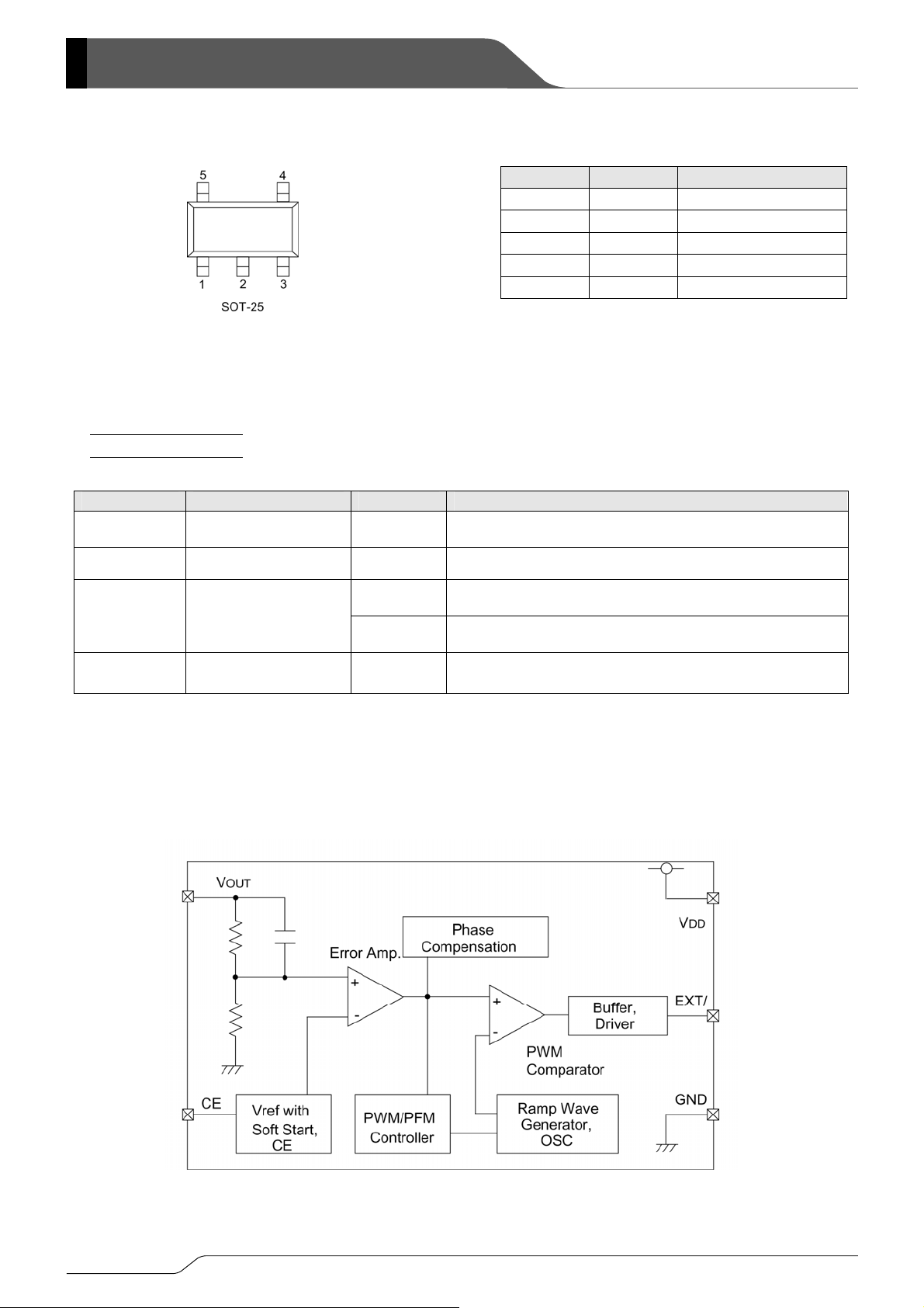
PIN CONFIGURATION
PRODUCT CLASSIFICATION
●Ordering Information
XC9301①②③④⑤⑥-⑦
XC9302①②③④⑤⑥-⑦
(*1)
: PWM control
(*1)
: PWM/PFM switching control
DESIGNATOR DESCRIPTION SYMBOL DESCRIPTION
PIN ASSIGNMENT
PIN NUMBER PIN NAME FUNCTION
1 GND Ground
2 VDD Power Supply
3 EXT/ External Tr. Drive
4 VOUT Output Voltage Monitor
5 CE Chip Enable
①
②③
Standard A Fixed
Output Voltage 20~60
e.g. VOUT=3.0V→②=3, ③=0, VOUT=5.3V→②=5, ③=3
2 180kHz
④
Oscillation Frequency
3 300kHz
⑤⑥-⑦
(*1)
The “-G” suffix indicates that the products are Halogen and Antimony free as well as being fully RoHS compliant.
(*2)
The device orientation is fixed in its embossed tape pocket. For reverse orientation, please contact your local Torex sales office or
representative. (Standard orientation: ⑤R-⑦, Reverse orientation: ⑤L-⑦)
BLOCK DIAGRAM
Packages
Taping Type
(*2)
MR-G SOT-25
2/13

■
A
XC9301/XC9302
Series
BSOLUTE MAXIMUM RATINGS
PARAMETER SYMBOL RATINGS UNITS
VDD Pin Voltage VDD -0.3〜12.0 V
VOUT Pin Voltage VOUT -0.3〜12.0 V
CE Pin Voltage VCE -0.3〜12.0 V
EXT/ Pin Voltage VEXT/ -0.3〜VDD+0.3 V
EXT/ Pin Current IEXT/ ±100 mA
Power Dissipation Pd 150 mW
Operating Temperature Range Topr -40〜+85 ℃
Storage Temperature Range Tstg -40〜+125 ℃
Ta = 25℃
3/13
■
■
XC9301/XC9302 Series
ELECTRICAL CHARACTERISTICS
XC9301x332MR, XC9302x332MR
PARAMETER SYMBOL CONDITIONS MIN. TYP. MAX. UNITS
Output Voltage VOUT 3.218 3.300 3.383 V
Supply Voltage VDD 2.0 - 10.0 V
Supply Current 1 IDD1 VOUT=CE: Setting output voltage × 0.95 applied - 80 140 μA
Supply Current 2 IDD2 VOUT=CE: Setting output voltage + 0.5 applied - 15 26 μA
OUT: Setting output voltage × 0.95 applied,
Stand-By Current ISTB
Oscillation Frequency FOSC
Maximum Duty Ratio MAXDTY
PFM Duty Ratio
Efficiency
(*1)
PFMDTY No Load 15 25 35 %
(*2)
EFFI
V
CE=0V
DD=VOUT=CE:
V
Setting output voltage × 0.95 applied
DD=VOUT=CE:
V
Setting output voltage × 0.95 applied
DD=VIN=CE:
V
Setting output voltage × 0.95 applied
Soft-Start Time TSS 5.0 10.0 20.0 ms
CE 'H' Voltage VCEH VOUT: Setting output voltage × 0.95 applied 0.65 - - V
CE 'L' Voltage VCEL VOUT: Setting output voltage × 0.95 applied - - 0.20 V
EXT/ 'H' ON Resistance REXTBH Same as IDD1, VEXT/ = VOUT - 0.4V - 29 43 Ω
EXT/ 'L' ON Resistance REXTBL Same as IDD1, VEXT/ = 0.4V - 19 27 Ω
Test Conditions: Unless otherwise stated, VDD = 3.3V, IOUT = 130mA
NOTE: *1: XC9302 series only
*2: EFFI={[(output voltage) × (output current)] / [(input voltage) × (input current)]} × 100
XC9301x333MR, XC9302x333MR
(VOUT=3.3V, FOSC=300kHz) Ta=25℃
PARAMETER SYMBOL CONDITIONS MIN. TYP. MAX. UNITS
Output Voltage VOUT 3.218 3.300 3.383 V
Supply Voltage VDD 2.0 - 10.0 V
Supply Current 1 IDD1 VOUT=CE: Setting output voltage × 0.95 applied - 130 200 μA
Supply Current 2 IDD2 VOUT=CE: Setting output voltage + 0.5 applied - 20 35 μA
OUT: Setting output voltage × 0.95 applied,
Stand-By Current ISTB
Oscillation Frequency FOSC
Max. Duty Ratio MAXDTY
PFM Duty Ratio
Efficiency
(*1)
PFMDTY No Load 15 25 35 %
(*2)
EFFI VDD=VIN=CE:
V
CE=0V
DD=VOUT=CE:
V
Setting output voltage × 0.95 applied
DD=VOUT=CE:
V
Setting output voltage × 0.95 applied
Setting output voltage × 0.95 applied
Soft-Start Time TSS 5.0 10.0 20.0 ms
CE 'H' Voltage VCEH VOUT: Setting output voltage × 0.95 applied 0.65 - - V
CE 'L' Voltage VCEL VOUT: Setting output voltage × 0.95 applied - - 0.20 V
EXT/ 'H' ON Resistance REXTBH Same as IDD1, VEXT/ = VOUT - 0.4V - 29 43 Ω
EXT/ 'L' ON Resistance REXTBL Same as IDD1, VEXT/ = 0.4V - 19 27 Ω
Test Conditions: Unless otherwise stated, VDD = 3.3V, IOUT = 130mA
NOTE: *1: XC9302 series only
*2: EFFI={[(output voltage) × (output current)] / [(input voltage) × (input current)]} × 100
TYPICAL APPLICATION CIRCUIT
External Components
PSW: XP162A12 (SOT-89, TOREX)
NSW: XP161A12 (SOT-89, TOREX)
L : 22μH (CR54, SUMIDA)
SD : U2FWJ44N ( Schottky, TOSHIBA )
C
C
220μF (Electrolytic, NICHICON, PJ type)
(VOUT=3.3V, FOSC=180kHz)
- - 0.5 μA
153 180 207 kHz
78 85 92 %
- 78 - %
- - 0.5 μA
255 300 345 kHz
78 85 92 %
- 78 - %
L : 16V, 47μF×2 (Tantalum, MCE series, NICHICON )
IN : 16V, 22μF (Tantalum, MCE series, NICHICON )
Ta=25℃
4/13
 Loading...