

XC9254R Series
ETR0529-002
600mA Driver Tr. Built-In, Synchronous Step-Down DC/DC Converter
☆GreenOperation Compatible
■GENERAL DESCRIPTIO N
The XC9254R series is a group of synchronous-rectification type DC/DC converters with a built-in 0.42ΩP-channel MOS driver
transistor and 0.52ΩN-channel MOS switching transistor, designed to allow the use of ceramic capacitors. Operating voltage
range is from 2.0V to 6.0V. The XC9254R001 type has a fixed output voltage of 1.2V (accuracy: ±2.0%). The device provides
a high efficiency, stable power supply with an output current of 600mA to be configured using only a coil and two capacitors
connected externally. With the built-in oscillator, 1.2MHz is fixed internally. As for operation mode, the XC9254 R series is
automatic PWM/PFM switching control allowing fast response, low ripple and high efficiency over the full range of loads (from
light load to heavy load).
The soft start and current control functions are internally optimized. During stand-by, all circuits are shutdown to reduce current
consumption to as low as 1.0μA or less. With the built-in UVLO (Under Voltage Lock Out) function, the internal P-channel
MOS driver transistor is forced OFF when input voltage becomes 1.4V or lower.
Two types of package SOT-25 and USP-6C are available.
■APPLICATIONS
●Mobile phones, Smart phones
●Bluetooth headsets
●Mobile WiMAX PDAs, MIDs, UMPCs
●Portable game consoles
●Digital cameras, Camcorders
●MP3 Players, Portable Media Players
●Notebook computers
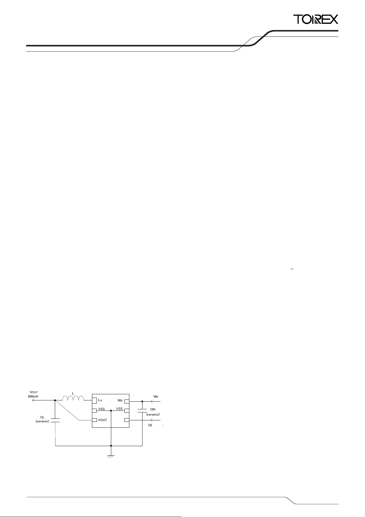
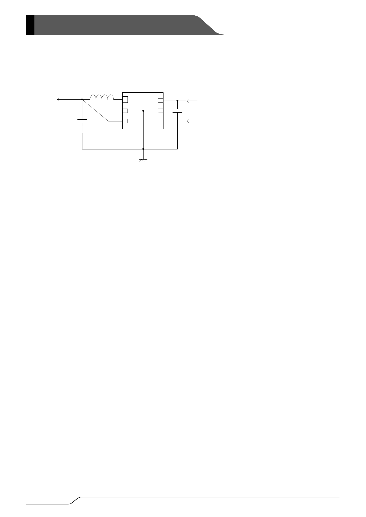
■TYPICAL APPLICA TION CIRCUIT
■FEATURES
Driver Transistor Built-In
Input Voltage : 2.0V ~ 6.0V
Output Voltage : 1.2V
High Efficiency : 92% (TYP.)
Output Current : 600mA
Oscillation Frequency : 1.2MHz (+15%)
Maximum Duty Cycle : 100%
Control Methods : PWM/PFM Auto
Function : Current Limiter Circuit Built-In
C
Capacitor
Operating Ambient Temperature
Packages : SOT-25, USP-6C
Environmentally Friendly : EU RoHS Compliant, Pb Free
* Performance depends on external components and wiring on the PCB.
: 0.42Ω P-ch driver transisto r
0.52Ω N-ch switch transistor
(Constant Current & Latching)
Discharge
L
: Low ESR Ceramic Capacitor
: -40℃ ~ +85℃
CE
1/17
XC9254R Series
■PIN CONFIGURATION
Lx VOUT
5 4
132
VSS CE/MODEVIN
CE/MODE 4
VIN 6
VSS 5
CE
1 Lx
2 VSS
3 VOUT (FB)
SOT-25
(Top View)
■PIN ASSIGNMENT
PIN NUMBER
SOT-25 USP-6C
1 6 VIN Power Input
2 2, 5 VSS Ground
3 4 CE High Active Enable
4 3 VOUT Fixed Output Voltage Pin
5 1 Lx Switching Output
USP-6C
(BOTTOM VIEW)
* Please short the VSS pin (No. 2 and 5).
* The dissipation pad for the USP-6C package should be solder-plated
in recommended mount pattern and metal masking so as to enhance
mounting strength and heat release. If the pad needs to be connected
to other pins, it should be connected to the V
(No. 5) pin.
SS
PIN NAME FUNCTION
2/17
■PRODUCT CLASSIFICATION
●Ordering Information
PWM / PFM automatic switching control
(*1)
The “-G” suffix indicates that the products are Halogen and Antimony free as well as being fully RoHS compliant.
PRODUCT NAME PACKAGE (ORDER UNIT)
XC9254R001MR-G
XC9254R001ER-G
(*1)
SOT-25 (3,000/Reel)
(*1)
USP-6C (3,000/Reel)
XC9254R
Series
3/17

A
XC9254R Series
■BLOCK DIAGRAM
VOUT
VIN
VSS
R2
R1
CFB
Error Amp.
FB
VSHORT
Vref with
Soft Start,
CE
UVLO
R3
R4
Phase
Compensation
PWM/PFM
Selector
UVLO Cmp
PWM
Comparator
Current Feedback
Current Limit
Logic
CE
Control
Logic
Synch
Buffer
Drive
Ramp Wave
Generator
OSC
Lx
CE/
CE
NOTE:
■
The signal from CE Control Logic to PWM/PFM Selector is being fixed to "H" level inside,
and XC9254R series chooses only PWM/PFM automatic switching control.
Diodes inside the circuit are ESD protection diodes and parasitic diodes.
BSOLUTE MAXIMUM RATINGS
PARAMETER SYMBOL RATINGS UNIT
VIN Pin Voltage VIN - 0.3 ~ 6.5 V
Lx Pin Voltage VLx - 0.3 ~ VIN + 0.3 ≦ 6.5V V
V
Pin Voltage V
OUT
CE Pin Voltage VCE - 0.3 ~ 6.5 V
Lx Pin Current ILx ±1500 mA
SOT-25 250 Power Dissipation
(*Ta=25℃)
USP-6C
Operating Ambient Temperature Topr - 40 ~ + 85
Storage Temperature Tstg - 55 ~ + 125
- 0.3 ~ 6.5 V
OUT
Pd
100
Ta=25℃
mW
O
C
O
C
4/17
XC9254R
■ELECTRICAL CHARACTERISTICS (Continued)
XC9254R Series, V
PARAMETER SYMBOL CONDITIONS MIN. TYP. MAX. UNIT
Output Voltage V
Operating Voltage Range VIN 2.0 - 6.0 V ①
Maximum Output Current I
UVLO Voltage V
Supply Current IDD V
Stand-by Current I
Oscillation Frequency f
PFM Switching Current I
PFM Duty Limit
Maximum Duty Cycle
Minimum Duty Cycle
Efficiency
Lx SW "H" ON Resistance 1 R
Lx SW "H" ON Resistance 2 R
Lx SW "L" ON Resistance 1 R
Lx SW "L" ON Resistance 2 R
Lx SW "H" Leak Current
Current Limit
Output Voltage
Temperature Characteristics
CE "H" Voltage V
CE "L" Voltage V
CE "H" Current I
CE "L" Current I
Soft Start Time tSS
Latch Time t
Short Protection Threshold
Test conditions: Unless otherwise stated, VIN=5.0V, V
NOTE:
Voltage
CL Discharge R
*1: Including hysteresis operating voltage range.
*2: EFFI = { ( output voltage×output current ) / ( input voltage×input current) }×100
*3: ON resistance (Ω)= (V
*4: R&D value
*5: When temperature is high, a current of approximately 10μA (maximum) may leak.
*6: Time until it short-circuits V
*7: When V
*8: When the difference between the input and the output is small, some cycles may be skipped completely before current maximizes.
*9: Current limit denotes the level of detection at peak of coil current.
*10: “H”=V
*11: V
IN
If current is further pulled from this state, output voltage will decrease because of P-ch driver ON resistance.
IN~VIN
is applied when V
IN
=1.2V, f
OUT
(*2)
EFFI
(*5)
I
(*9)
I
IN
is less than 2.4V, limit current may not be reached because voltage falls caused by ON resistance.
-1.2V, “L”=+0.1V~-0.1V
OUT (E)
=1.2MHz, Ta=25℃
OSC
When connected to external components,
DTY
DTY
OUT
OUTMAX
UVLO
STB
OSC
PFM
LIMIT_PFM
DTY
V
=5.0V, I
IN=VCE
V
IN=VOUT(E)
When connected to external components
=VIN, V
V
CE
Voltage which Lx pin holding “L” level
=5.0V, V
IN=VCE
VIN=5.0V, VCE=0V, V
When connected to external components,
V
IN=VOUT(E)
When connected to external components,
V
IN=VOUT(E)
=2.0V, I
V
CE=VIN
V
MAX
MIN
IN=VCE
V
IN=VCE
=5.0V, V
=5.0V, V
=30mA
OUT
+2.0V, VCE=1.0V,
OUT=VOUT(E)
×0.5V
OUT=VOUT(E)
OUT=VOUT(E)
+2.0V, VCE =1.0V, I
+2.0V, VCE =VIN, I
=1mA 200 % ①
OUT
OUT=VOUT(E)
OUT=VOUT(E)
(*8)
(*11)
(*1, *10)
×1.1V - 15 33 μA ③
×1.1V - 0 1.0 μA ③
=100mA
OUT
=1mA
OUT
×0.9V 100 - - % ②
×1.1V - - 0 % ②
When connected to external components,
(V
V
CE=VIN=VOUT(E)
VIN=VCE=5.0V, V
LxH
VIN=VCE=3.6V, V
LxH
VIN=VCE=5.0V
LxL
VIN=VCE=3.6V
LxL
VIN=V
LeakH
V
LIM
△V
OUT
・△Topr)
OUT
CEH
CEL
VIN=VCE=5.0V,
CEH
VIN=5.0V, VCE=0V,
CEL
IN=VCE
/
I
OUT
V
OUT
Voltage changes Lx to “H” level
V
OUT
Voltage changes Lx to “L” level
OUT
=30mA, -40℃≦Topr≦85℃ - ±100 -
=
V
=
V
+1.2V, I
OUT (E)
OUT (E)
(*4)
- 0.45 0.66 Ω ④
(*4)
=100mA
OUT
×0.9V , ILx=100mA
×0.9V , ILx=100mA
(*3)
(*3)
=5.0V, VCE=0V, Lx=0V - 0.01 1.0 μA ⑤
=5.0V, V
OUT(E)
OUT(E)
OUT=VOUT(E)
×0.9V, Applied voltage to VCE,
×0.9V, Applied voltage to VCE ,
V
=
V
OUT
OUT(E)
V
=
V
OUT
OUT(E)
(*7)
×0.9V
900 1050 1350 mA ⑥
(*10)
(*10)
×0.9V - 0.1 - 0.1 μA ⑤
×0.9V - 0.1 - 0.1 μA ⑤
When connected to external components,
V
=0V → VIN, I
CE
=5.0V, V
V
LAT
IN=VCE
Short Lx at 1Ω resistance
Sweeping V
V
SHORT
DCHG
- Lx pin measurement voltage) / 100mA
with GND via 1Ωof resistor from an operational state and is set to Lx=0V from current limit pulse generating.
OUT
x 0.5V becomes more than VIN.
1
Ω
resistance, V
level within 1ms
VIN=5.0V, LX=5.0V, VCE=0V, V
=Nominal Voltage, applied voltage sequence is V
OUT(E)
=1mA
OUT
=0.8×V
OUT
, VIN=VCE=5.0V, Short Lx at
OUT
voltage which Lx becomes “L”
OUT
,
OUT(E)
(*6)
=open 200 300 450 Ω ⑧
OUT
1.176 1.200 1.224 V ①
600 - - mA ①
1.00 1.40 1.78 V ②
1020 1200 1380 kHz ①
140 180 240 mA ①
- 92 - % ①
- 0.35 0.55 Ω ④
- 0.42 0.67 Ω ④
- 0.52 0.77 Ω -
0.65 - 6.0 V ③
V
SS
0.5 1.0 2.5 ms ①
1.0 - 20.0 ms ⑦
0.675 0.900 1.150 V ⑦
OUT→VIN→VCE
ppm/
- 0.25 V ③
℃
Series
CIRCUIT
①
5/17
XC9254R Series
■TYPICAL APPLICATION CIRCUIT
V
OUT
600mA
C
L
(ceramic)
L
Lx
VSS
VOUT
V
VSS
CE/
CE
MODE
IN
V
C
IN
(ceramic)
CE/ MO DE
CE
●f
=1.2MHz
OSC
L:
CL:
4.7μH
4.7μF
10μF
IN
CIN:
(NR4018, TAIYO YUDEN)
(Ceramic)
(Ceramic)
6/17

XC9254R
Series
■OPERATIONAL DESCRIPTION
The XC9254R series consists of a reference voltage source, ramp wave circuit, error amplifier, PWM comparator, phase
compensation circuit, output voltage adjustment resistors, P-channel MOS driver transistor, N-channel MOS switching
transistor for the synchronous switch, current limiter circuit, UVLO circuit and others. (See the block diagram above.) The
series ICs compare, using the error amplifier, the voltage of the internal voltage reference source with the feedback voltage
from the V
to input a signal to the PWM comparator to determine the turn-on time during PWM operation. The PWM comparator
compares, in terms of voltage level, the signal from the error amplifier with the ramp wave from the ramp wave circuit, and
delivers the resulting output to the buffer driver circuit to cause the Lx pin to output a switching duty cycle. This process is
continuously performed to ensure stable output voltage. The current feedback circuit monitors the P-channel MOS driver
transistor current for each switching operation, and modulates the error amplifier output signal to provide multiple feedback
signals. This enables a stable feedback loop even when a low ESR capacitor such as a ceramic capacitor is used ensu ring
stable output voltage.
<Reference Voltage Source>
The reference voltage source provides the reference voltage to ensure stable output voltage of the DC/DC converter.
<Ramp Wave Circuit>
The ramp wave circuit determines switching frequency. The frequency is fixed internally as 1.2MHz. Clock pulses generated
in this circuit are used to produce ramp waveforms needed for PWM operation, and to synchronize all the internal circuits.
<Error Amplifier>
The error amplifier is designed to monitor output voltage. The amplifier compares the reference voltage with the feedback
voltage divided by the internal split resistors, R1 and R2. When a voltage lower than the reference voltage is fed back, the
output voltage of the error amplifier increases. The gain and frequency characteristics o f the error amplifier output are fixed
internally to deliver an optimized signal to the mixer.
<Current Limit>
The current limiter circuit of the XC9254R series monitors the current flowing through the P-channel MOS driver transistor
connected to the Lx pin, and features a combination of the current limit mode and the operation suspension mode.
① When the driver current is greater than a specific level, the current limit function operates to turn off the pulses from the Lx
② When the driver transistor is turned off, the limiter circuit is then released from the current limit detection state.
③ At the next pulse, the driver transistor is turned on. However, the transistor is immediately turned off in the case of an over
④ When the over current state is eliminated, the IC resumes its normal operation.
OUT pin through split resistors, R1 and R2. Phase compensation is performed on the resulting error amplifier output,
pin at any given timing.
current state.
The IC waits for the over current state to end by repeating the steps ① through ③. If an over current state continues for a
few ms and the above three steps are repeatedly performed, the IC performs the function of latching the OFF state of the
driver transistor, and goes into operation suspension mode. Once the IC is in suspension mode, operations can be
resumed by either turning the IC off via the CE/MODE pin, or by restoring power to the V
not mean a complete shutdown, but a state in which pulse output is suspended; therefore, the internal circuitry remains in
operation. T he current limit of the XC9254R series can be set at 1050mA at typical. Besides, care must be taken when
laying out the PC Board, in order to prevent misoperation of the current limit mode. Depending on the state of the PC
Board, latch time may become longer and latch operation may not work. In order to avoid the effect of noise, the board
should be laid out so that input capacitors are placed as close to the IC as possible.
pin. The suspension mode does
IN
7/17

XC9254R Series
■OPERATIONAL DESCRIPTION (Continued)
<Short-Circuit Protection>
The short-circuit protection circuit monitors the internal R1 and R2 divider voltage from the V
the block diagram shown in the previous page). In case where output is accidentally shorted to the Ground and when
the FB point voltage decreases less than half of the reference voltage (Vref) and a current more than the I
the Pch MOS driver transistor, the short-circuit protection quickly operates to turn off and to latch the driver transistor.
In latch mode, the operation can be resumed by either turning the IC off and on via the CE pin, or by restoring power
supply to the V
When sharp load transient happens, a voltage drop at the V
short circuit protection may operate in the voltage higher than 1/2 V
<UVLO Circuit>
When the V
prevent false pulse output caused by unstable operation of the interna l circuitry. When the V
or higher, switching operation takes place. By releasing the UVLO function, the IC performs the soft start function to
initiate output startup operation. The soft start function operates even when the VIN pin volta ge falls momentarily below
the UVLO operating voltage. The UVLO circuit does not cause a complete shutdown of the IC, but causes pulse output to
be suspended; therefore, the internal circuitry remains in operation.
<PFM Switch Current>
In PFM control operation, until coil current reaches to a specified level (I
on. In this case, time that the Pch MOS driver transistor is kept on (t
t
= L×IPFM / (VIN-VOUT) →IPFM①
ON
< PFM Duty Limit >
In PFM control operation, the PFM duty limit (
duty increases (e.g. the condition that the step-down ratio is small), it’s possible for Pch MOS driver transistor to be turned
off even when coil current doesn’t reach to IPFM. →IPFM②
pin.
IN
IN pin voltage becomes 1.4V or lower, the Pch MOS driver transistor output driver transistor is forced OFF to
DTY
LIMIT_PFM
t
Ton
ON
is propagated to the FB point through CFB, as a result,
OUT
voltage.
OUT
PFM), the IC keeps the Pch MOS driver transistor
) can be given by the following formula.
ON
) is set to 200% (TYP.). Therefore, under the cond ition that the
PFM Duty Limit
PFMデューティ制限
pin (refer to FB point in
OUT
flows to
LIM
pin voltage becomes 1.8V
IN
Lx
I Lx
図 IPFM ①
PFM
I
0mA
Lx
I Lx
FOSC
f
OSC
図 IPFM ②
IPFM
0mA
8/17

XC9254R
■OPERATIONAL DESCRIPTION (Continued)
<CL High Speed Discharge>
The XC9254R series can quickly discharge the electric charge at the outpu t capacitor (C
which enables a whole IC circuit put into OFF state, is inputted via the Nch MOS switch transistor located between the L
pin and the VSS pin. When the IC is disabled, electric charge at the output capacitor (CL) is quickly discharged so that it may
avoid application malfunction. Discharge time of the output capacitor (C
and the output capacitor (C
value (CL) as τ(τ=C x R), discharge time of the output voltage after discharge via the N channel transistor is calculated
by the following formulas.
V = V
OUT(E)
V : Output voltage after discharge
V
OUT(E)
t: Discharge time,
τ: C x R
–t/
τ
x e
or t=τln (V
: Output voltage
C= Capacitance of Output capacitor (CL)
R= C
auto-discharge resistance
L
). By setting time constant of a CL auto-discharge resistance value (R) and an output capacitor
L
/ V)
OUT(E)
) is set by the CL auto-discharge resistance (R)
L
) when a low signal to the CE pin
L
Series
X
Output Voltage Dischage Characteristics
Rdischg
100
90
80
70
60
50
40
30
20
10
0
0 102030405060708090100
= 300Ω TYP
()
CL=10uF
CL=20uF
CL=50uF
Discharge Time t (ms)
9/17

XC9254R Series
■OPERATIONAL DESCRIPTION (Continued)
<CE Pin Function>
The operation of the XC9254R series will enter into the shut do wn mode when a low level signal is input to the CE pin. Durin g
the shutdown mode, the current consumption of the IC becomes 0μA (TYP.), with a state of high impedance at the Lx pin and
V
OUT pin. The IC starts its operation by inputting a high level signal to the CE pin. The input to the CE pin is a CMOS input and
the sink current is 0μA (TYP.).
●Examples of how to use CE pin
(A)
SW_CE
ON Stand-by
OFF Operation
(B)
SW_CE
ON Operation
OFF Stand-by
<Soft Start>
The XC9254R series provide 1.0ms (TYP).
Soft start time is defined as the time interval to reach 90% of the output voltage from the time when the CE pin is turned on.
■FUNCTION CHART
CE VOLTAGE LEVEL OPERATIONAL STATES
10/17
STATUS
STATUS
tSS
Synchronous
H Level
L Level Stand-by
PWM/PFM
Automatic Switching
CE
(A)
90% of setting voltage
CE
(B)

XC9254R
Series
■NOTE ON USE
1. The XC9254R series is designed for use with ceramic output capacitors. If, however, the potential difference is too large
between the input voltage and the output voltage, a ceramic capacitor may fail to absorb the resulting high switching energy
and oscillation could occur on the output. If the input-output potential difference is large, connect an electrolytic capacitor
in parallel to compensate for insufficient capacitance.
2. Spike noise and ripple voltage arise in a switching regulator as with a DC/DC converter. These are greatly influenced by
external component selection, such as the coil inductance, capacitance values, and board layout of external components.
Once the design has been completed, verification with actual components should be done.
3. Depending on the input-output voltage differential, or load current, some pulses may be skipped, and the ripple voltage may
increase.
4. When the difference between V
possibility that some cycles may be skipped completely.
5. When the difference between V
there is the possibility that some cycles may be skipped completely.
6. With the IC, the peak current of the coil is controlled by the current limit circuit. Since the peak current increases when
dropout voltage or load current is high, current limit starts operation, and this can lead to instability. When peak current
becomes high, please adjust the coil inductance value and fully check the circuit operation. In addition, please calculate
the peak current according to the following formula:
Ipk = (V
L: Coil Inductance Value
f
7. When the peak current which exceeds limit current flows within the specified time, the built-in Pch MOS driver transistor
turns off. During the time until it detects limit current and before the built-in transistor can be turned off, the current for limit
current flows; therefore, care must be taken when selecting the rating for the external components such as a coil.
8. When V
9. Care must be taken when laying out the PC Board, in order to prevent misoperation of the current limit mode. Depending
on the state of the PC Board, latch time may become longer and latch operation may not work. In order to avoid the effect of
noise, the board should be laid out so that input capacitors are placed as close to the IC as possible.
10. Use of the IC at voltages below the recommended voltage range may lead to instability.
11. This IC should be used within the stated absolute maximum ratings in order to prevent damage to the device.
12. When the IC is used in high temperature, output voltage may increase up to input voltage level at no load because of the
leak current of the driver transistor.
13. The current limit is set to 1350mA (MAX.)
①Current flows into Pch MOS driver transistor to reach the current limit (I
②The current of ILIM or more flows since the delay time of the circuit occurs during from t he detection of the current lim it to
③Because of no potential difference at both ends of the coil, the time rate of coil current becomes quite small.
④Lx oscillates very narrow pulses by the current limit for several ms.
⑤The circuit is latched, stopping its operation.
IN - VOUT) x OnDuty / (2 x L x f
: Oscillation Frequency
OSC
IN is less than 2.4V, limit current may not be reached because voltage falls caused by ON resistance.
current limit functions while the VOUT pin is shorted to the GND pin, when Pch MOS driver transistor is ON, the potential
difference for input voltage will occur at both ends of a coil. For this, the time rate of coil current becomes large. By
contrast, when Nch MOS driver transistor is ON, there is almost no potential difference at both ends of the coil since the
OUT pin is shorted to the GND pin. Consequently, the time rate of coil current becomes quite small. According to the
V
repetition of this operation, and the delay time of the circuit, coil current will be converged on a certain current value,
exceeding the amount of current, which is supposed to be limited originally. Even in this case, however, after the over
current state continues for several ms, the circuit will be latched. A coil should be used within the stated absolute
maximum rating in order to prevent damage to the device.
OFF of Pch MOS driver transistor.
LX
ILIM
ILX
IN and VOUT is large in PWM control, very narrow pulses will be outputted, and there is the
IN and VOUT is small, and the load current is heavy, very wide pulses will be outputted and
) + IOUT
OSC
at typical. However, the current of 1350mA or more may flow. In case that the
LIM).
④
Limit > # mS
ms
⑤
①
②
③
Delay
11/17

XC9254R Series
■NOTE ON USE (Continued)
14. In order to stabilize VIN’s voltage level and oscillation frequency, we recommend that a by-pass capacitor (CIN) be
connected as close as possible to the V
15. High step-down ratio and very light load may lead an intermittent oscillation.
16. During PWM / PFM automatic switching mode, operating may become unstable at transition to continuous mode.
Please verify with actual parts.
17. Please note the inductance value of the coil. The IC may enter unstable operation if the combination of ambient
temperature, setting voltage, oscillation frequency, and L value are not adequate.
In the operation range close to the maximum duty cycle, The IC may happen to enter unstable output voltage operation
even if using the L values listed below.
●The Range of L Value
f
V
OSC
1.2MHz V
*When a coil less value of 4.7μH is used at f
current limit I
. In this case, it may happen that the IC can not provide 600mA output current.
LMI
OUT
OUT
=1.2V
18. It may happen to enter unstable operation when the IC operation mode goes into continuous op eration mode under the
condition of small input-output voltage difference. Care must be taken with the actual design unit.
IN & VSS pins.
L Value
3.3μH~6.8μH
=1.2MHz, peak coil current more easily reach the
OSC
12/17

XC9254R
■NOTE ON USE (Continued)
●Instructions of pattern layouts
1. In order to stabilize VIN voltage level, we recommend that a by-pass capacitor (CIN) be connected as close as possible to
the VIN & VSS pins.
2. Please mount each external component as close to the IC as possible.
3. Wire external components as close to the IC as possible and use thick, short connecting traces to reduce the circuit
impedance.
4. Make sure that the PCB GND traces are as thick as possible, as variations in ground potential caused by high ground
currents at the time of switching may result in instability of the IC.
5. This series’ internal driver transistors bring on heat because of the output current and ON resistance of driver transistors.
XC9235/36/37A,B,C(出力電圧固定品)
(PKG:SOT-25)
XC9235/36/37A,B,C,E,G(出力電圧固定品)
(PKG: USP-6C)
(PKG:USP-6C/USP-6EL)
Series
VIN
CIN
VSS
CE
For the VIN, V
L
VOUT
IC
CL
VSS
, VSS/CE, please put the wire.
OUT
。VIN,VOUT,VSS,CEには使用しやすいように電線等を付けてご使用下さい
Ceramic_Cap
インダクタ
Inductor
Inductor
VOUT
CE
VSS
For the VIN, V
L
CIN
IC
VIN
VSS
, VSS/CE, please put the wire.
OUT
。VIN,VOUT,VSS,CEには使用しやすいように電線等を付けてご使用下さい
Ceramic_Cap
Inductor
Inductor
インダクタ
13/17

XC9254R Series
■TEST CIRCUITS
< Circuit No.1 >
・A/B/C/E/G series ・D/F series
A
CIN
VIN Lx
CE/MODE VOUT
VSS
※ Exte rnal Components
L : 1.5uH(NR3015) 3.0MHz
4.7uH(NR4018) 1.2MHz
CIN : 4.7μF(ceramic)
CL :10μF(ceramic)
< Circuit No.2 >
A
1uF
VIN Lx
VSS
VOUT
(FB)
CE/MODE
< Circuit No.4 >
1uF
VIN Lx
VSS
VOUT
(FB)
CE/MODE
< Circuit No.6 >
1uF
VIN Lx
VSS
VOUT
(FB)
CE/MODE
< Circuit No.8 >
1uF
VIN Lx
VSS
VOUT
(FB)
CE/MODE
Wave Form Measure Point
L
V
CL
V
ON resistance = (VIN-VLx)/100mA
Wave Form Measure Point
V
ILx
A
RL
< Circuit No.3 >
< Circuit No.5 >
100mA
< Circuit No.7 >
ILIM
< Circuit No.9 >
A
※ Exte rnal Components
L : 1.5μH(NR4018) 3.0MHz V
: 4.7μH (NR3015) 1.2MH z
CIN : 4.7μF
CL : 10μF
R1 : 150kΩ
R2 : 300kΩ
Cfb : 120pF
1uF
A
VIN Lx
CIN
CE/MODE
1uF
ICEH
A
ICEL
1uF
CIN
VIN Lx
CE/MODE
VIN Lx
CE/MODE
VIN Lx
CE/MODE
VIN Lx
CE/MODE
VSS
OUT=VFB×(R1+R2)/R2
VSS
VSS
VSS
VSS
FB
VOUT
VOUT
VOUT
(FB)
(FB)
VOUT
(FB)
(FB)
L
A
Wave Form Measure Point
Cfb
R1
CL
R2
Wave Form Measure Point
Rpulldown
200Ω
Wave Form Measure Point
Ilat
Rpulldown
1Ω
IOUT
V
RL
14/17

■PACKAGING INFORMATION
●SOT-25
●USP-6C Reference Pattern Layout
0.05
2.4
0.45
6
5
4
0.05
1.0
0.45
1
2
3
●USP-6C
●USP-6C Reference Metal Mask Design
XC9254R
Series
15/17

XC9254R Series
■MARKING RULE
●SOT-25, USP-6C
SOT-25
(TOP VIEW)
④ ⑤
② ③①
USP-6C/USP-6EL
USP-6C
(Top View)
(TOP VIEW)
① represent product series
PRODUCT SERIES MARK
XC9254R L
② represents integer numb er of output voltage and oscillation frequency
MARK OUTPUT
VOLTAGE (V)
f
=1.2MHz
OSC
1.X B
③ represents decimal point of output voltage
V
(V) MARK
OUT
X.20 2
④⑤ represents production lot number
Order of 01, …09, 10, 11, …99, 0A, …0Z, 1A, …9Z, A0, …Z9, AA, …ZZ.
(G, I, J, O, Q, W excluded)
*No character inversion used.
16/17

XC9254R
Series
1. The products and product specifications contained he rein are subject to change without
notice to improve performance characteristics. Consult us, or our representatives
before use, to confirm that the information in this datasheet is up to date.
2. We assume no responsibility for any infringement of patents, patent rights, or other
rights arising from the use of any information and circuitry in this datasheet.
3. Please ensure suitable shipping controls (including fail-safe designs and aging
protection) are in force for equipment employing products listed in this datasheet.
4. The products in this datasheet are not developed, designed, or approved for use with
such equipment whose failure of malfunction can be reasonably expected to directly
endanger the life of, or cause significant injury to, the user.
(e.g. Atomic energy; aerospace; transport; combustion and associated safety
equipment thereof.)
5. Please use the products listed in this dat asheet within the specified ranges.
Should you wish to use the products under conditions exceeding the specifications,
please consult us or our representatives.
6. We assume no responsibility for damage or loss due to abnormal use.
7. All rights reserved. No part of this datasheet may be copied or reproduced without the
prior permission of TOREX SEMICONDUCTOR LTD.
17/17
 Loading...