

TOREX XC9244, XC9245 User Manual
g
XC9244/XC9245 Series
400mA Synchronous Step-Down DC/DC Converters
■GENERAL DESCRIPTION
The XC9244/XC9245 series is a group of synchronous-rectification type step-down DC/DC converters with a built-in
0.65Ω P-channel MOS driver transistor and 0.45Ω N-channel MOS switching transistor, designed to allow the use of
ceramic capacitors. Output current of 400mA (MAX.) to be configured using only a coil and capacitor connected externally.
The output voltage can be set from 0.8V to 4.0V in increments of 0.05V (accuracy: ±2.0%). With an internal switching
frequency of 1.2MHz, small external components can be used. USPN-6 package is suitable for the application which
requires low profile and small-footprint.
The XC9244 series is PWM fixed frequency control, and the XC9245 series is PWM/PFM, which automatically switches
from PWM to PFM during light loads, high efficiency can be achieved over a wide range of load conditions. When
stand-by mode, due to stop all operation, supply current is reduced to 1μA or less. The integrated C
which enables the electric charge at the output capacitor CL to be discharged via the internal discharge switch located
between the V
stand-by mode.
The XC9244/XC9245 series has a high speed soft-start as fast as 0.25ms in typical for quick turn-on. Current limiter
circuit (Constant Current & Latching) is built-in for preventing from thermal destruction. With UVLO (Under Voltage Lock
Out) function, the internal P channel driver transistor is forced OFF when input voltage becomes 2.25V or lower.
■APPLICATIONS
●Mobile phones
●
Bluetooth headsets
●
Mobile internet devices
●Portable game consoles
●Digital cameras, Camcorders
●Codeless phones
●
Notebook computers
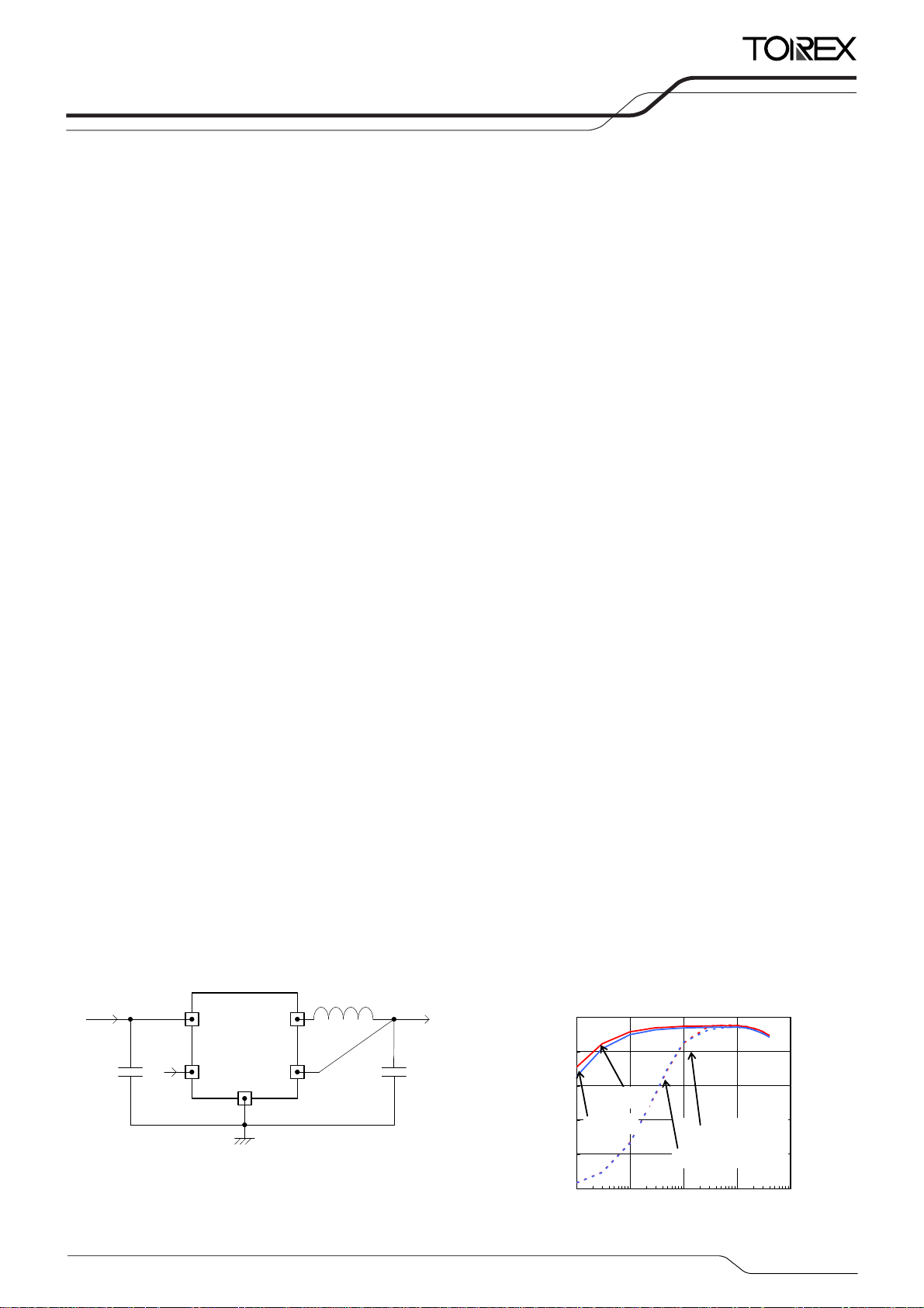
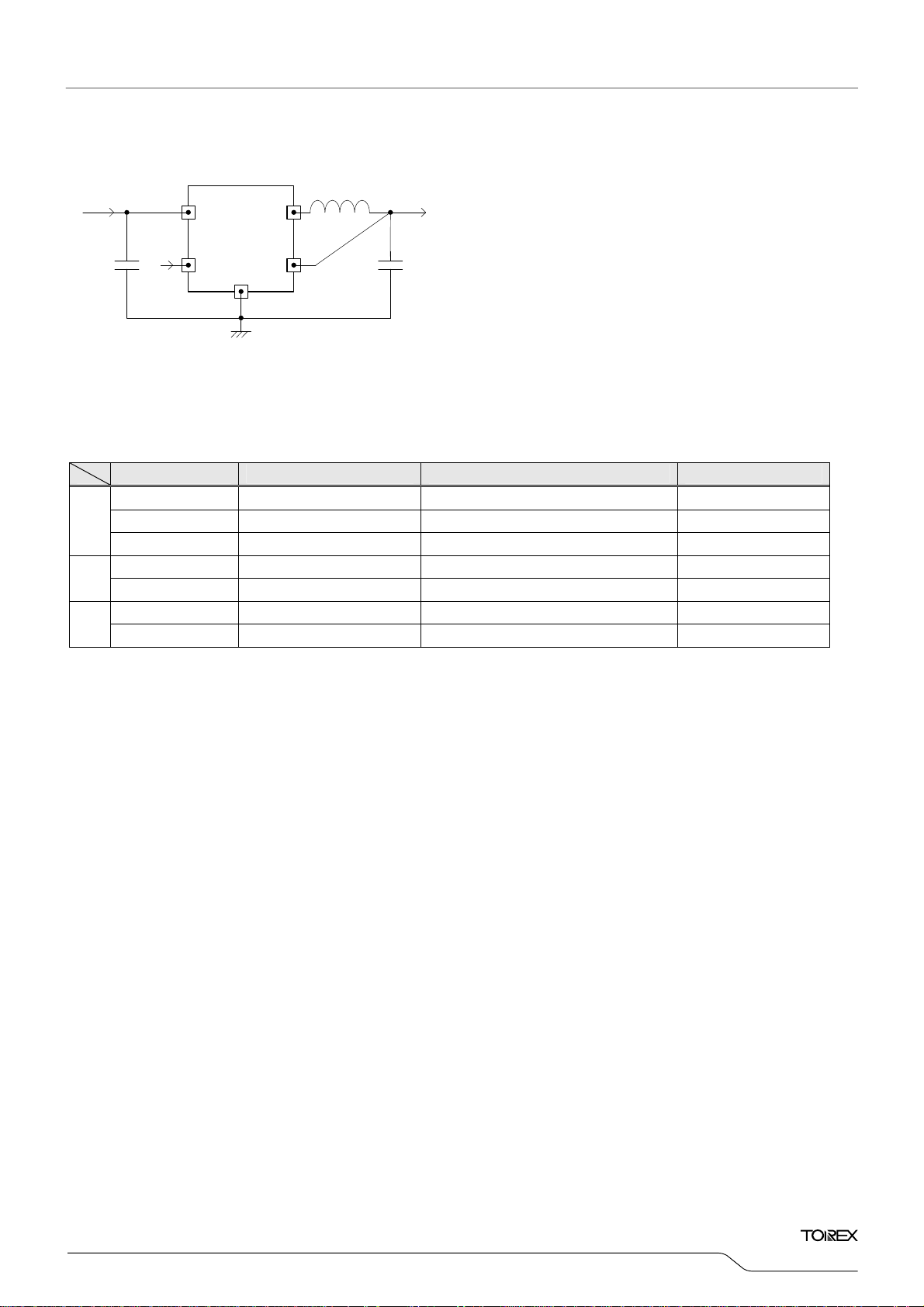
■TYPICAL APPLICATION CIRCUIT
VIN
CIN
(ceramic)
and VSS pins. The CL discharge function prevents malfunction on V
OUT
■FEATURES
Driver Transistor Built-In
Input Voltage : 2.3V ~ 6.0V
Output Voltage Selectable
High Efficiency :
Output Current : 400mA
Oscillation Frequency : 1.2MHz ±15%
Maximum Duty Cycle : 100%
Function :
Capacitor : Low ESR Ceramic Capacitor
Control Methods : PWM (XC9244)
Operating Ambient Temperature
Package : USPN-6
Environmentally Friendly
* The characteristics chan
■TYPICAL PERFORMANCE
CHARACTERISTICS
V
L
V
IN
CE
CE
Lx
V
OUT
V
SS
OUT
400mA
(ceramic)
100
80
CL
60
40
Efficiency : EFFI (%)
20
☆GreenOperation Compatible
L
connecting application during
OUT
:
0.65Ω P-ch Driver Transistor
0.45Ω N-ch Synchronous Switch Transistor
:
0.8V ~ 4.0V (0.05V Increments)
90% (TYP.)
Current Limiter Circuit
(Constant Current & Latching)
C
High Speed Discharge
L
Soft Start Circuit
PWM/PFM Auto (XC9245)
: -40℃~+85℃
: EU RoHS Compliant, Pb Free
e with external parts, substrate wiring, etc.
XC9244/XC9245A33C
CIN=4.7μF(LMK212BJ475)
L=4.7μH(SPM3012),C
VIN=4.2V
VIN=5.0V
=10μF(LMK212BJ106)
L
PWM Control
=4.2V
V
IN
5.0V
ETR0520-004
discharge function
*
0
0.1 1 10 100 1000
Output Current : I
OUT
(mA)
1/24

(*1)
XC9244/XC9245 Series
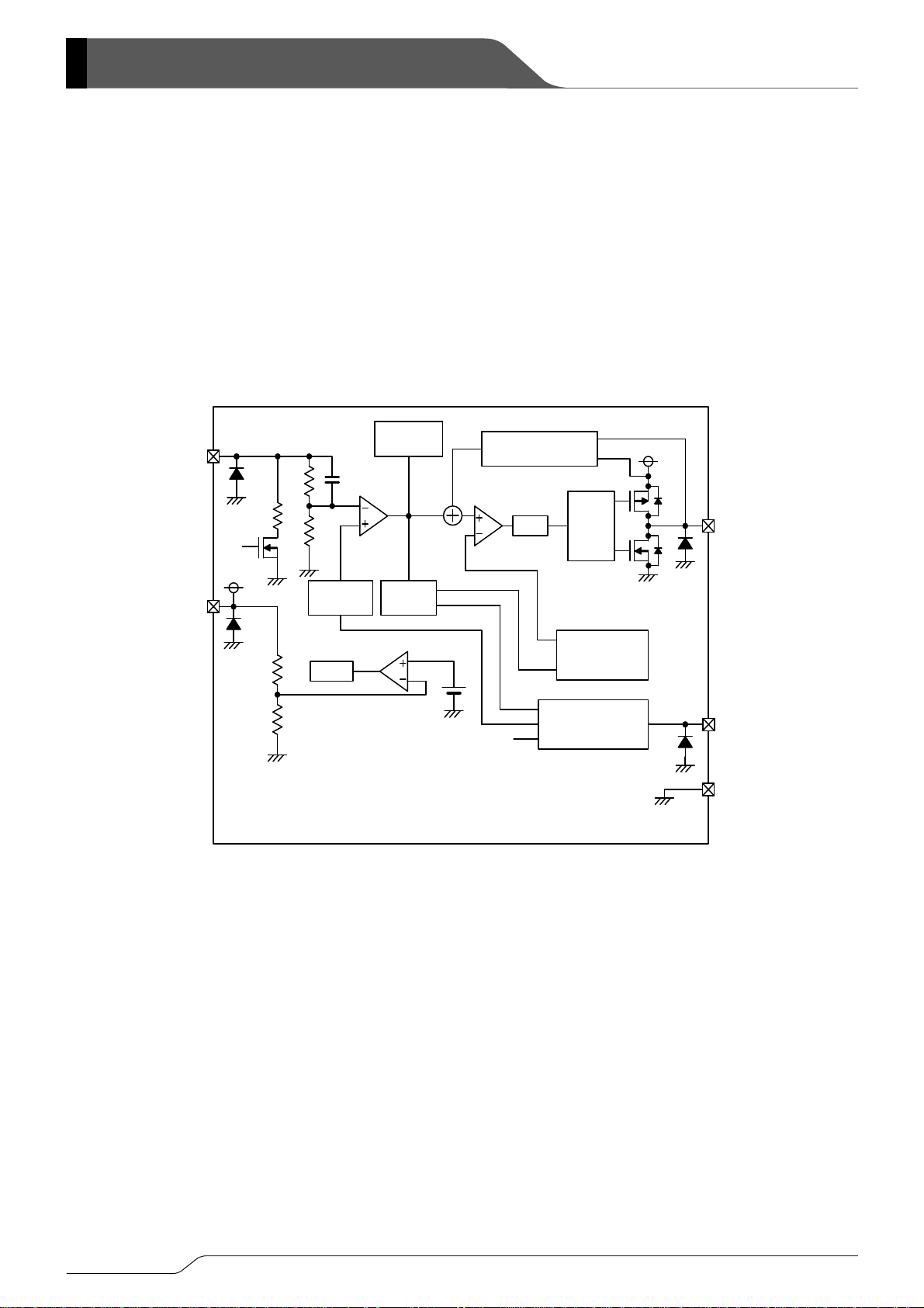
■BLOCK DIAGRAM
XC9244/XC9245 Series, Type A
■PRODUCT CLASSIFICATION
●Ordering Information
XC9244①②③④⑤⑥-⑦ Fixed PWM control
XC9245①②③④⑤⑥-⑦ PWM / PFM automatic switching control
DESIGNATOR ITEM SYMBOL DESCRIPTION
①
②③
④
⑤⑥-⑦
The “-G” suffix denotes Halogen and Antimony free as well as being fully RoHS compliant.
Selection Guide
TYPE
(*1)
OUTPUT
VOLTAGE
Package (Order Unit) 7R-G USPN-6 (5,000/Reel)
Type A Refer to Selection Guide
Output voltage options
e.g. 1.2V → ②=1, ③=2
Output Voltage
Oscillation
Frequency
CL
AUTO-DISCHARGE
08~40
C 1.2MHz
LATCH UVLO
1.25V → ②=2, ③=C
0.05V increments: 0.05=A, 0.15=B, 0.25=C, 0.35=D, 0.45=E,
0.55=F, 0.65=H, 0.75=K, 0.85=L, 0.95=M
Refer to “Stadard Voltage”
CHIP
ENABLE
CURRENT
LIMIT
SOFT-START TIME
A Fixed Yes Yes Yes Yes Yes Fixed
Standard Voltage
V
(V)
OUT
1.0V XC9244A10C7R-G XC9245A10C7R-G
1.2V XC9244A12C7R-G XC9245A12C7R-G
1.5V XC9244A15C7R-G XC9245A15C7R-G
1.8V XC9244A18C7R-G XC9245A18C7R-G
2.5V XC9244A25C7R-G XC9245A25C7R-G
2.8V XC9244A28C7R-G XC9245A28C7R-G
3.3V XC9244A33C7R-G XC9245A33C7R-G
Fixed PWM PWM/PFM Auto
PRODUCT NAME
*For other voltages, please contact your local Torex sales office or representative.
2/24
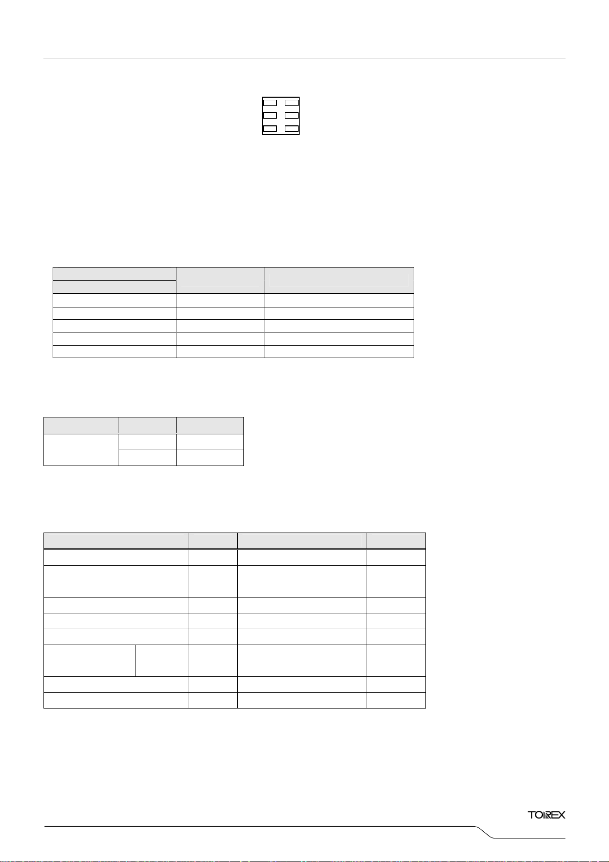
■PIN CONFIGURATION
*If the pad needs to be connected to other pins, it should be connected to the VSS (No. 2 and 6) pin.
SS 6
V
Lx 5
V
IN 4
USPN-6
(BOTTOM VIEW)
1 VOUT
2 VSS
3 CE
■PIN ASSIGNMENT
PIN NUMBER
USPN-6
4 VIN Power Input
2, 6 VSS Ground
3 CE Chip Enable
1 V
5 LX Switching Output
PIN NAME FUNCTION
Output Voltage Monitor
OUT
XC9244/XC9245
Series
■FUNCTION
XC9244/XC9245 Series, Type A
PIN NAME SIGNAL STATUS
CE
* Please do not leave the CE pin open.
L Stand-by
H Active
■ABSOLUTE MAXIMUM RATINGS
Ta=25℃
PARAMETER SYMBOL RATINGS UNITS
VIN Pin Voltage VIN
Lx Pin Voltage VLx
V
Pin Voltage V
OUT
CE Pin Voltage VCE
Lx Pin Current ILx ±1500 mA
Power Dissipation USPN-6 Pd 100 mW
OUT
-0.3~+6.5
-0.3~VIN+0.3 or +6.5
-0.3~VIN+0.3 or +6.5
-0.3~ +6.5
(*1)
(*1)
V
V
V
V
Operating Ambient Temperature Topr
Storage Temperature Tstg
* All voltages are described based on the VSS pin.
(*1) The maximum value should be either V
+0.3 or +6.5 in the lowest.
IN
-40~+85 ℃
-55~+125 ℃
3/24
XC9244/XC9245 Series
■ELECTRICAL CHARACTERISTICS
XC9244/XC9245 Ta=25℃
PARAMETER SYMBOL CONDITIONS MIN. TYP. MAX.
Output Voltage V
OUT
When connected to external components,
VIN=VCE=5.0V, I
OUT
=30mA
<E-1> <E-2> <E-3> V ①
Operating Voltage Range VIN 2.3 - 6.0 V ①
Maximum Output Current I
UVLO Voltage V
OUTMAX
UVLO
Quiescent Current Iq VIN=VCE=5.0V, V
Stand-by Current I
Oscillation Frequency f
PFM Switch Current
PFM Duty Limit
(*3)
I
(*3)
DTY
Maximum Duty Cycle D
Minimum Duty Cycle D
STB
OSC
PFM
LIMIT_PFM
MAX
MIN
Efficiency EFFI
Lx SW”H”ON Resistance R
Lx SW”L”ON Resistance R
Lx SW”H” Leakage Current
Lx SW”L” Leakage Current
Current Limit
(*7)
I
(*7)
I
(*8)
I
Output Voltage Temperature
Characteristics
LXH
LXL
LeakH
LeakL
V
LIM
ΔV
OUT
(V
・
ΔTopr)
OUT
When connected to external components
(*1)
,VIN=VCE=V
V
V
IN=VCE,VOUT
holding “L” level
=5.0V, VCE=0V, V
IN
When connected to external components,
VIN=VCE=5.0V, I
When connected to external components,
VIN=V
= (C-1) , I
CE
VIN=VCE= (C-2), I
VIN=V
=5.0V, V
CE
VIN=VCE=5.0V, V
+2.0V,
OUT(E)
=0V,Voltage which Lx pin
(*2,*9)
OUT=VOUT(E)
OUT
=200mA
OUT
=1mA
OUT
=1mA - - 300 % ①
OUT
OUT=VOUT(E)
OUT=VOUT(E)
When connected to external components,
V
IN=VCE=VOUT(E)
VIN=VCE=5.0V, V
V
IN=VCE
VIN=V
VIN=V
IN=VCE
/
I
=30mA, -40℃≦Topr≦85℃ - ±100 -
OUT
+1.5V, I
OUT
=0V, ILX=100mA
OUT
=5.0V - 0.45
=5.0V, VCE=0V, VLX=0V - 0.00 1.00 μA ⑤
OUT
=5.0V, VCE=0V, VLX=5.0V - 0.00 1.00 μA ⑤
OUT
=5.0V, V
OUT=VOUT(E)
400 - - mA ①
1.60 1.90 2.25 V ③
× 1.1V - 18 30 μA ②
=0V - 0.0 1.0 μA ②
1020 1200 1380 kHz ①
125 180 235 mA ①
× 0.9V 100 - - % ③
× 1.1V - - 0 % ③
=100mA
(*4)
(*5)
- <E-4> - % ①
- 0.65 0.85 Ω ④
(*6)
0.65
×0.9V 700 900 1200 mA ⑥
UNITS CIRCUIT
(*6)
Ω -
ppm/
℃
①
=5.0V, V
V
CE ”H” Voltage V
CE ”L” Voltage V
CE ”H” Current I
CE ”L” Current I
CEH
CEL
V
CEH
V
CEL
Soft-Start Time tSS
Latch Time t
CL Discharge R
NOTE:
Unless otherwise stated, V
(*1) When the difference between the input and the output is small, some cycles may be skipped completely before current maximizes.
If current is further pulled from this state, output voltage will decrease because of P-ch driver ON resistance.
(*2) Including UVLO detect voltage, hysteresis operating voltage range for UVLO release voltage. UVLO release voltage is V
Lx pin becomes “H”.
(*3) XC9244 series exclude I
(*4) EFFI = { ( output voltage×output current ) / ( input voltage×input current) }×100
(*5) ON resistance= (V
=5.0V, V
IN
- Lx pin measurement voltage) / 100mA
IN
and DTY
PFM
OUT(E)
LAT
DCHG
=Nominal Voltage
because those are only for the PFM control’s functions.
LIMIT_PFM
IN
,Voltage changes Lx to “H” level
V
CE
=5.0V, V
V
IN
V
,Voltage changes Lx to “L” level
CE
=5.0V, VCE=5.0V, V
IN
=5.0V, VCE=0V, V
IN
When connected to external components,
=5.0V, VCE=0V → 5.0V, I
V
IN
V
IN=VCE
Short Lx at 1Ω resistance
VIN=5.0V, VCE=0V, V
=0V, Applied voltage to
OUT
=0V, Applied voltage to
OUT
OUT
OUT
=5.0V, V
OUT
=0.8×V
OUT
(*9)
(*9)
1.20 - 6.00 V ③
VSS - 0.25 V ③
=0V -0.1 - 0.1 μA ⑤
=0V -0.1 - 0.1 μA ⑤
OUT
=1mA
OUT(E)
(*10)
,
- 0.25 - ms ①
0.50 1.00 5.00 ms ⑦
=5.0V 50 120 200 Ω ⑧
voltage which is
IN
(*6) Design value
(*7) When temperature is high, a current of approximately 10μA (maximum) may leak.
(*8)Current limit denotes the level of detection at peak of coil current.
(*9) "H"=V
(*10) Time until it short-circuits V
- 1.2V, "L"=+ 0.1V ~ - 0.1V
IN~VIN
OUT
with GND via 1Ωof resistor from an operational state and is set to Lx=0V from current limit pulse generating.
4/24
■ELECTRICAL CHARACTERISTICS (Continued)
SPEC Table
1) I
PFM
,DTY
LIMIT_PFM,VOUT
,EFFI
XC9244/XC9245
Series
NOMINAL
OUTPUT
VOLTAGE
V
OUT(E)
0.80 0.784 0.800 0.816 77
0.85 0.833 0.850 0.867 78
0.90 0.882 0.900 0.918 79
0.95 0.931 0.950 0.969 80
1.00 0.980 1.000 1.020 81
1.05 1.029 1.050 1.071 82
1.10 1.078 1.100 1.122 83
1.15 1.127 1.150 1.173 84
1.20 1.176 1.200 1.224 85
1.25 1.225 1.250 1.275 85
1.30 1.274 1.300 1.326 86
1.35 1.323 1.350 1.377 86
1.40 1.372 1.400 1.428 86
1.45 1.421 1.450 1.479 86
1.50 1.470 1.500 1.530 87
1.55 1.519 1.550 1.581 87
1.60
1.65 1.617 1.650 1.683 87
1.70 1.666 1.700 1.734 88
1.75
1.80 1.764 1.800 1.836 88
1.85 1.813 1.850 1.887 88
1.90 1.862 1.900 1.938 89
1.95 1.911 1.950 1.989 89
2.00 1.960 2.000 2.040 89
2.05 2.009 2.050 2.091 89
2.10 2.058 2.100 2.142 89
2.15 2.107 2.150 2.193 90
2.20 2.156 2.200 2.244 90
2.25 2.205 2.250 2.295 90
2.30 2.254 2.300 2.346 90
2.35 2.303 2.350 2.397 90
2.40 2.352 2.400 2.448 91
2.45 2.401 2.450 2.499 91
2.50 2.450 2.500 2.550 91
2.55 2.499 2.550 2.601 91
2.60 2.548 2.600 2.652 91
2.65 2.597 2.650 2.703 91
2.70
I
DTY
PFM
<C-1> <C-2>
3.6V
V
+2.0V
OUT(E)
V
OUT(E)
LIMIT_PFM
2.3V
+0.5V
V
<E-1> <E-2> <E-3>
MIN. TYP. MAX.
1.568 1.600 1.632 87
1.715 1.750 1.785 88
2.646 2.700 2.754 92
EFFI (TYP.)
OUT
<E-4>
5/24
XC9244/XC9245 Series
■ELECTRICAL CHARACTERISTICS (Continued)
SPEC Table
,DTY
1) I
PFM
LIMIT_PFM,VOUT
NOMINAL
OUTPUT
VOLTAGE
V
OUT(E)
2.75 2.695 2.750 2.805 92
2.80 2.744 2.800 2.856 92
2.85 2.793 2.850 2.907 92
2.90 2.842 2.900 2.958 92
2.95 2.891 2.950 3.009 92
3.00 2.940 3.000 3.060 92
3.05 2.989 3.050 3.111 92
3.10 3.038 3.100 3.162 93
3.15 3.087 3.150 3.213 93
3.20 3.136 3.200 3.264 93
3.25 3.185 3.250 3.315 93
3.30 3.234 3.300 3.366 93
3.35 3.283 3.350 3.417 93
3.40 3.332 3.400 3.468 93
3.45 3.381 3.450 3.519 93
3.50 3.430 3.500 3.570 93
3.55 3.479 3.550 3.621 93
3.60 3.528 3.600 3.672 93
3.65 3.577 3.650 3.723 93
3.70 3.626 3.700 3.774 93
3.75 3.675 3.750 3.825 94
3.80 3.724 3.800 3.876 94
3.85 3.773 3.850 3.927 94
3.90 3.822 3.900 3.978 94
3.95 3.871 3.950 4.029 94
4.00
V
OUT(E)
,EFFI
I
DTY
PFM
<C-1> <C-2>
+2.0V V
OUT(E)
LIMIT_PFM
+0.5V
V
<E-1> <E-2> <E-3>
MIN. TYP. MAX.
3.920 4.000 4.080 94
OUT
EFFI
(TYP.)
<E-4>
6/24
XC9244/XC9245
■TYPICAL APPLICATION CIRCUIT
VIN
CIN
(ceramic)
L
V
IN
CE
CE
Lx
V
OUT
V
SS
V
OUT
400mA
(ceramic)
CL
●External Components
MANUFACTURE PRODUCT NUMBER RATED VOLTAGE / INDUCTANCE DIMENTION (mm)
TDK SPM3012-4R7
L
TAIYO YUDEN NR3015-4R7
Coilcraft EPL3015-4R7
CIN
TAIYO YUDEN LMK212ABJ475KG
KYOCERA CM105X5R475K10A
TAIYO YUDEN LMK212ABJ106KG
CL
KYOCERA CM105X5R106M10A
4.7μH
4.7μH
4.7μH
10V / 4.7μF
10V / 4.7μF
10V / 10μF
10V / 10μF
3.2 x 3.0 x h1.2
3.0 x 3.0 x h1.5
3.2 x 3.2 x h1.55
2.0 x 1.25 x h1.4
1.6 x 0.8 x h1.0
2.0 x 1.25 x h1.4
1.6 x 0.8 x h1.0
Series
7/24
XC9244/XC9245 Series
■OPERATIONAL DESCRIPTION
The XC9244/XC9245 series consists of a reference voltage source, ramp wave circuit, error amplifier, PWM comparator, phase compensation
circuit, output voltage adjustment resistors, P-channel MOS driver transistor, N-channel MOS switching transistor for the synchronous switch,
current limiter circuit, UVLO circuit and others. (See the block diagram below.)
The series ICs compare, using the error amplifier, the voltage of the internal voltage reference source with the feedback voltage from the V
pin through split resistors, R1 and R2. Phase compensation is performed on the resulting error amplifier output, to input a signal to the PWM
comparator to determine the turn-on time during PWM operation. The PWM comparator compares, in terms of voltage level, the signal from the
error amplifier with the ramp wave from the ramp wave circuit, and delivers the resulting output to the buffer driver circuit to cause the Lx pin to
output a switching duty cycle. This process is continuously performed to ensure stable output voltage. The current feedback circuit monitors
the P-channel MOS driver transistor current for each switching operation, and modulates the error amplifier output signal to provide multiple
feedback signals. This enables a stable feedback loop even when a low ESR capacitor such as a ceramic capacitor is used ensuring stable
output voltage.
XC9244/XC9245 Series, Type A
VOUT
R1
CEB
IN
V
R2
Vref with
Soft Start,
CE
UVLO
R3
R4
<Reference Voltage Source>
The reference voltage source provides the reference voltage to ensure stable output voltage of the DC/DC converter.
<Ramp Wave Circuit>
The ramp wave circuit determines switching frequency. The frequency is fixed internally as1.2MHz. Clock pulses generated in this circuit are
used to produce ramp waveforms needed for PWM operation, and to synchronize all the internal circuits.
<Error Amplifier>
The error amplifier is designed to monitor output voltage. The amplifier compares the reference voltage with the feedback voltage divided by the
internal split resistors, R1 and R2. When a voltage lower than the reference voltage is fed back, the output voltage of the error amplifier
increases. The gain and frequency characteristics of the error amplifier output are fixed internally to deliver an optimized signal to the mixer.
The error amplifier output signal optimized in the mixer is modulated with the current feedback signal. This signal is delivered to the PWM
compatator.
C
FB
Error Amp.
UVLO Comparator
Phase
Compensation
PWM/PFM
Selector
Current Feedback
Current Limit
PWM
Comparator
CEB
Logic
Synch.
Buffer
Drive
Ramp Wave
Generator
OSC
CE
Control
Logic
Lx
CE
V
SS
OUT
8/24
 Loading...