

g
XC9244/XC9245 Series
400mA Synchronous Step-Down DC/DC Converters
■GENERAL DESCRIPTION
The XC9244/XC9245 series is a group of synchronous-rectification type step-down DC/DC converters with a built-in
0.65Ω P-channel MOS driver transistor and 0.45Ω N-channel MOS switching transistor, designed to allow the use of
ceramic capacitors. Output current of 400mA (MAX.) to be configured using only a coil and capacitor connected externally.
The output voltage can be set from 0.8V to 4.0V in increments of 0.05V (accuracy: ±2.0%). With an internal switching
frequency of 1.2MHz, small external components can be used. USPN-6 package is suitable for the application which
requires low profile and small-footprint.
The XC9244 series is PWM fixed frequency control, and the XC9245 series is PWM/PFM, which automatically switches
from PWM to PFM during light loads, high efficiency can be achieved over a wide range of load conditions. When
stand-by mode, due to stop all operation, supply current is reduced to 1μA or less. The integrated C
which enables the electric charge at the output capacitor CL to be discharged via the internal discharge switch located
between the V
stand-by mode.
The XC9244/XC9245 series has a high speed soft-start as fast as 0.25ms in typical for quick turn-on. Current limiter
circuit (Constant Current & Latching) is built-in for preventing from thermal destruction. With UVLO (Under Voltage Lock
Out) function, the internal P channel driver transistor is forced OFF when input voltage becomes 2.25V or lower.
■APPLICATIONS
●Mobile phones
●
Bluetooth headsets
●
Mobile internet devices
●Portable game consoles
●Digital cameras, Camcorders
●Codeless phones
●
Notebook computers
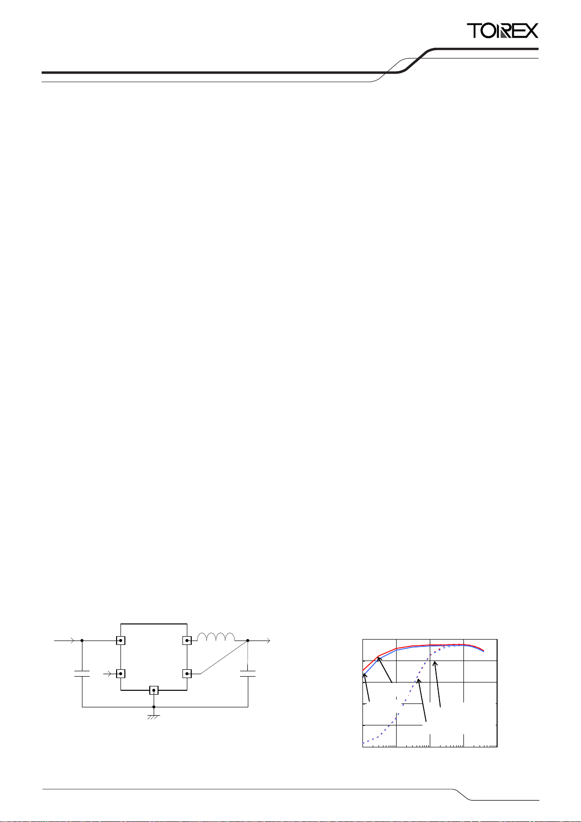
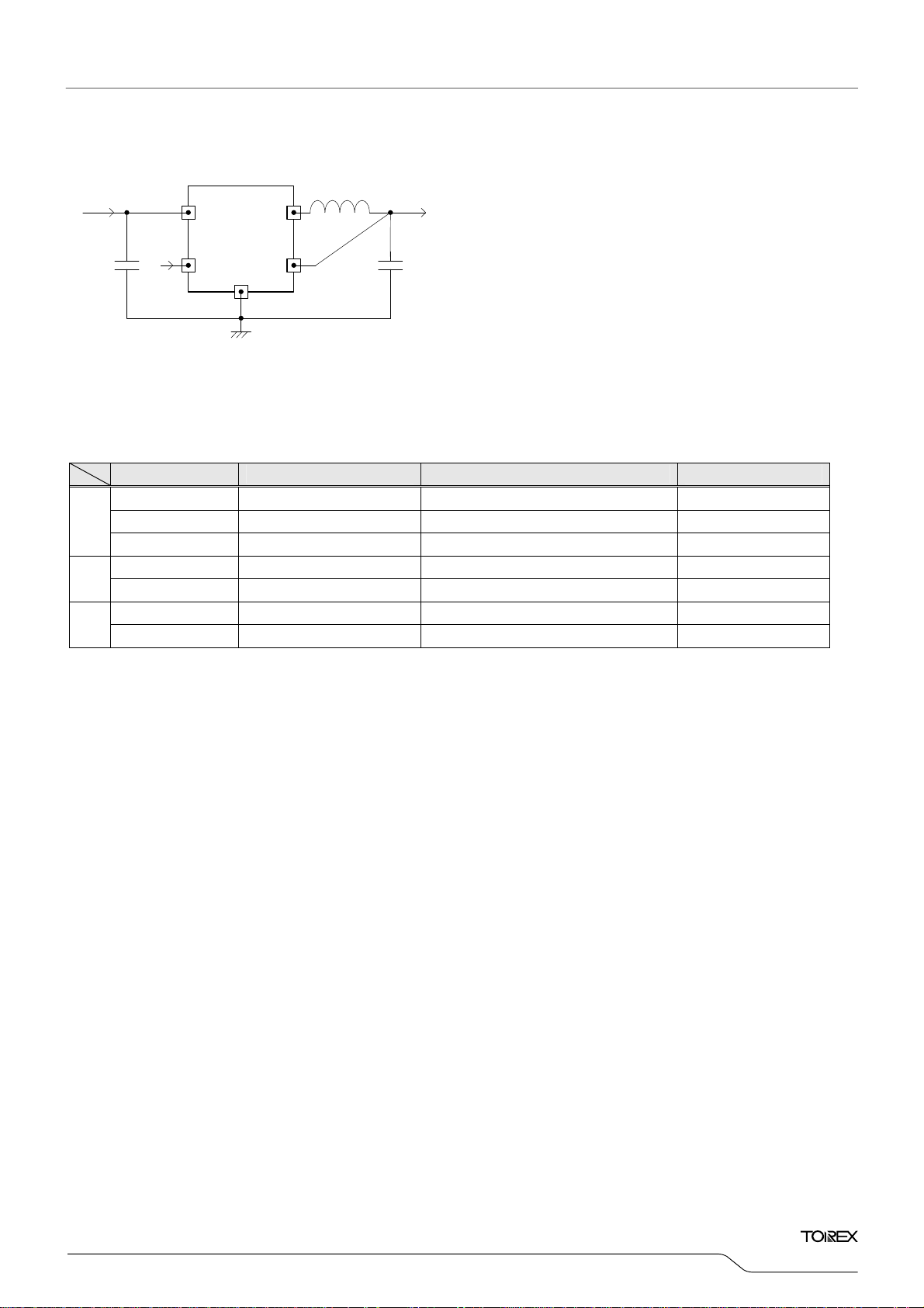
■TYPICAL APPLICATION CIRCUIT
VIN
CIN
(ceramic)
and VSS pins. The CL discharge function prevents malfunction on V
OUT
■FEATURES
Driver Transistor Built-In
Input Voltage : 2.3V ~ 6.0V
Output Voltage Selectable
High Efficiency :
Output Current : 400mA
Oscillation Frequency : 1.2MHz ±15%
Maximum Duty Cycle : 100%
Function :
Capacitor : Low ESR Ceramic Capacitor
Control Methods : PWM (XC9244)
Operating Ambient Temperature
Package : USPN-6
Environmentally Friendly
* The characteristics chan
■TYPICAL PERFORMANCE
CHARACTERISTICS
V
L
V
IN
CE
CE
Lx
V
OUT
V
SS
OUT
400mA
(ceramic)
100
80
CL
60
40
Efficiency : EFFI (%)
20
☆GreenOperation Compatible
L
connecting application during
OUT
:
0.65Ω P-ch Driver Transistor
0.45Ω N-ch Synchronous Switch Transistor
:
0.8V ~ 4.0V (0.05V Increments)
90% (TYP.)
Current Limiter Circuit
(Constant Current & Latching)
C
High Speed Discharge
L
Soft Start Circuit
PWM/PFM Auto (XC9245)
: -40℃~+85℃
: EU RoHS Compliant, Pb Free
e with external parts, substrate wiring, etc.
XC9244/XC9245A33C
CIN=4.7μF(LMK212BJ475)
L=4.7μH(SPM3012),C
VIN=4.2V
VIN=5.0V
=10μF(LMK212BJ106)
L
PWM Control
=4.2V
V
IN
5.0V
ETR0520-004
discharge function
*
0
0.1 1 10 100 1000
Output Current : I
OUT
(mA)
1/24

(*1)
XC9244/XC9245 Series
■BLOCK DIAGRAM
XC9244/XC9245 Series, Type A
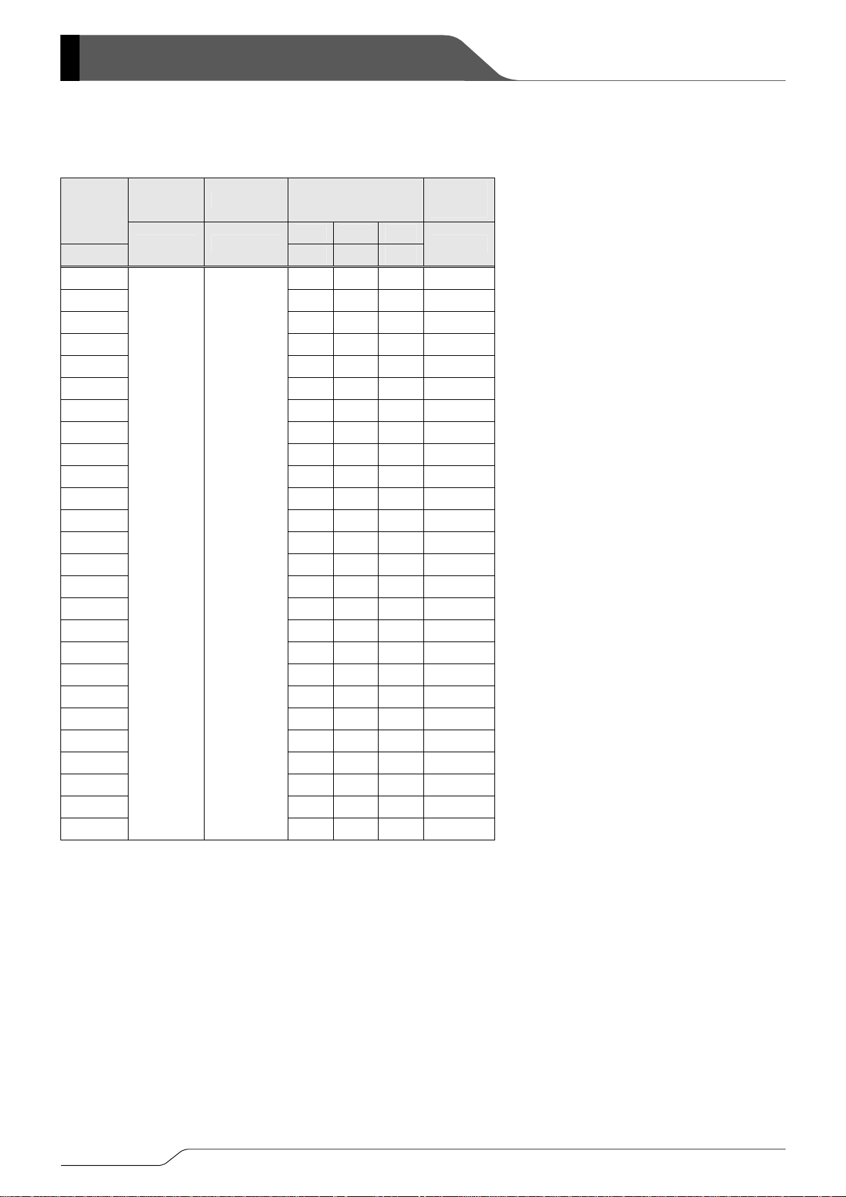
■PRODUCT CLASSIFICATION
●Ordering Information
XC9244①②③④⑤⑥-⑦ Fixed PWM control
XC9245①②③④⑤⑥-⑦ PWM / PFM automatic switching control
DESIGNATOR ITEM SYMBOL DESCRIPTION
①
②③
④
⑤⑥-⑦
The “-G” suffix denotes Halogen and Antimony free as well as being fully RoHS compliant.
Selection Guide
TYPE
(*1)
OUTPUT
VOLTAGE
Package (Order Unit) 7R-G USPN-6 (5,000/Reel)
Type A Refer to Selection Guide
Output voltage options
e.g. 1.2V → ②=1, ③=2
Output Voltage
Oscillation
Frequency
CL
AUTO-DISCHARGE
08~40
C 1.2MHz
LATCH UVLO
1.25V → ②=2, ③=C
0.05V increments: 0.05=A, 0.15=B, 0.25=C, 0.35=D, 0.45=E,
0.55=F, 0.65=H, 0.75=K, 0.85=L, 0.95=M
Refer to “Stadard Voltage”
CHIP
ENABLE
CURRENT
LIMIT
SOFT-START TIME
A Fixed Yes Yes Yes Yes Yes Fixed
Standard Voltage
V
(V)
OUT
1.0V XC9244A10C7R-G XC9245A10C7R-G
1.2V XC9244A12C7R-G XC9245A12C7R-G
1.5V XC9244A15C7R-G XC9245A15C7R-G
1.8V XC9244A18C7R-G XC9245A18C7R-G
2.5V XC9244A25C7R-G XC9245A25C7R-G
2.8V XC9244A28C7R-G XC9245A28C7R-G
3.3V XC9244A33C7R-G XC9245A33C7R-G
Fixed PWM PWM/PFM Auto
PRODUCT NAME
*For other voltages, please contact your local Torex sales office or representative.
2/24
■PIN CONFIGURATION
*If the pad needs to be connected to other pins, it should be connected to the VSS (No. 2 and 6) pin.
SS 6
V
Lx 5
V
IN 4
USPN-6
(BOTTOM VIEW)
1 VOUT
2 VSS
3 CE
■PIN ASSIGNMENT
PIN NUMBER
USPN-6
4 VIN Power Input
2, 6 VSS Ground
3 CE Chip Enable
1 V
5 LX Switching Output
PIN NAME FUNCTION
Output Voltage Monitor
OUT
XC9244/XC9245
Series
■FUNCTION
XC9244/XC9245 Series, Type A
PIN NAME SIGNAL STATUS
CE
* Please do not leave the CE pin open.
L Stand-by
H Active
■ABSOLUTE MAXIMUM RATINGS
Ta=25℃
PARAMETER SYMBOL RATINGS UNITS
VIN Pin Voltage VIN
Lx Pin Voltage VLx
V
Pin Voltage V
OUT
CE Pin Voltage VCE
Lx Pin Current ILx ±1500 mA
Power Dissipation USPN-6 Pd 100 mW
OUT
-0.3~+6.5
-0.3~VIN+0.3 or +6.5
-0.3~VIN+0.3 or +6.5
-0.3~ +6.5
(*1)
(*1)
V
V
V
V
Operating Ambient Temperature Topr
Storage Temperature Tstg
* All voltages are described based on the VSS pin.
(*1) The maximum value should be either V
+0.3 or +6.5 in the lowest.
IN
-40~+85 ℃
-55~+125 ℃
3/24
XC9244/XC9245 Series
■ELECTRICAL CHARACTERISTICS
XC9244/XC9245 Ta=25℃
PARAMETER SYMBOL CONDITIONS MIN. TYP. MAX.
Output Voltage V
OUT
When connected to external components,
VIN=VCE=5.0V, I
OUT
=30mA
<E-1> <E-2> <E-3> V ①
Operating Voltage Range VIN 2.3 - 6.0 V ①
Maximum Output Current I
UVLO Voltage V
OUTMAX
UVLO
Quiescent Current Iq VIN=VCE=5.0V, V
Stand-by Current I
Oscillation Frequency f
PFM Switch Current
PFM Duty Limit
(*3)
I
(*3)
DTY
Maximum Duty Cycle D
Minimum Duty Cycle D
STB
OSC
PFM
LIMIT_PFM
MAX
MIN
Efficiency EFFI
Lx SW”H”ON Resistance R
Lx SW”L”ON Resistance R
Lx SW”H” Leakage Current
Lx SW”L” Leakage Current
Current Limit
(*7)
I
(*7)
I
(*8)
I
Output Voltage Temperature
Characteristics
LXH
LXL
LeakH
LeakL
V
LIM
ΔV
OUT
(V
・
ΔTopr)
OUT
When connected to external components
(*1)
,VIN=VCE=V
V
V
IN=VCE,VOUT
holding “L” level
=5.0V, VCE=0V, V
IN
When connected to external components,
VIN=VCE=5.0V, I
When connected to external components,
VIN=V
= (C-1) , I
CE
VIN=VCE= (C-2), I
VIN=V
=5.0V, V
CE
VIN=VCE=5.0V, V
+2.0V,
OUT(E)
=0V,Voltage which Lx pin
(*2,*9)
OUT=VOUT(E)
OUT
=200mA
OUT
=1mA
OUT
=1mA - - 300 % ①
OUT
OUT=VOUT(E)
OUT=VOUT(E)
When connected to external components,
V
IN=VCE=VOUT(E)
VIN=VCE=5.0V, V
V
IN=VCE
VIN=V
VIN=V
IN=VCE
/
I
=30mA, -40℃≦Topr≦85℃ - ±100 -
OUT
+1.5V, I
OUT
=0V, ILX=100mA
OUT
=5.0V - 0.45
=5.0V, VCE=0V, VLX=0V - 0.00 1.00 μA ⑤
OUT
=5.0V, VCE=0V, VLX=5.0V - 0.00 1.00 μA ⑤
OUT
=5.0V, V
OUT=VOUT(E)
400 - - mA ①
1.60 1.90 2.25 V ③
× 1.1V - 18 30 μA ②
=0V - 0.0 1.0 μA ②
1020 1200 1380 kHz ①
125 180 235 mA ①
× 0.9V 100 - - % ③
× 1.1V - - 0 % ③
=100mA
(*4)
(*5)
- <E-4> - % ①
- 0.65 0.85 Ω ④
(*6)
0.65
×0.9V 700 900 1200 mA ⑥
UNITS CIRCUIT
(*6)
Ω -
ppm/
℃
①
=5.0V, V
V
CE ”H” Voltage V
CE ”L” Voltage V
CE ”H” Current I
CE ”L” Current I
CEH
CEL
V
CEH
V
CEL
Soft-Start Time tSS
Latch Time t
CL Discharge R
NOTE:
Unless otherwise stated, V
(*1) When the difference between the input and the output is small, some cycles may be skipped completely before current maximizes.
If current is further pulled from this state, output voltage will decrease because of P-ch driver ON resistance.
(*2) Including UVLO detect voltage, hysteresis operating voltage range for UVLO release voltage. UVLO release voltage is V
Lx pin becomes “H”.
(*3) XC9244 series exclude I
(*4) EFFI = { ( output voltage×output current ) / ( input voltage×input current) }×100
(*5) ON resistance= (V
=5.0V, V
IN
- Lx pin measurement voltage) / 100mA
IN
and DTY
PFM
OUT(E)
LAT
DCHG
=Nominal Voltage
because those are only for the PFM control’s functions.
LIMIT_PFM
IN
,Voltage changes Lx to “H” level
V
CE
=5.0V, V
V
IN
V
,Voltage changes Lx to “L” level
CE
=5.0V, VCE=5.0V, V
IN
=5.0V, VCE=0V, V
IN
When connected to external components,
=5.0V, VCE=0V → 5.0V, I
V
IN
V
IN=VCE
Short Lx at 1Ω resistance
VIN=5.0V, VCE=0V, V
=0V, Applied voltage to
OUT
=0V, Applied voltage to
OUT
OUT
OUT
=5.0V, V
OUT
=0.8×V
OUT
(*9)
(*9)
1.20 - 6.00 V ③
VSS - 0.25 V ③
=0V -0.1 - 0.1 μA ⑤
=0V -0.1 - 0.1 μA ⑤
OUT
=1mA
OUT(E)
(*10)
,
- 0.25 - ms ①
0.50 1.00 5.00 ms ⑦
=5.0V 50 120 200 Ω ⑧
voltage which is
IN
(*6) Design value
(*7) When temperature is high, a current of approximately 10μA (maximum) may leak.
(*8)Current limit denotes the level of detection at peak of coil current.
(*9) "H"=V
(*10) Time until it short-circuits V
- 1.2V, "L"=+ 0.1V ~ - 0.1V
IN~VIN
OUT
with GND via 1Ωof resistor from an operational state and is set to Lx=0V from current limit pulse generating.
4/24
■ELECTRICAL CHARACTERISTICS (Continued)
SPEC Table
1) I
PFM
,DTY
LIMIT_PFM,VOUT
,EFFI
XC9244/XC9245
Series
NOMINAL
OUTPUT
VOLTAGE
V
OUT(E)
0.80 0.784 0.800 0.816 77
0.85 0.833 0.850 0.867 78
0.90 0.882 0.900 0.918 79
0.95 0.931 0.950 0.969 80
1.00 0.980 1.000 1.020 81
1.05 1.029 1.050 1.071 82
1.10 1.078 1.100 1.122 83
1.15 1.127 1.150 1.173 84
1.20 1.176 1.200 1.224 85
1.25 1.225 1.250 1.275 85
1.30 1.274 1.300 1.326 86
1.35 1.323 1.350 1.377 86
1.40 1.372 1.400 1.428 86
1.45 1.421 1.450 1.479 86
1.50 1.470 1.500 1.530 87
1.55 1.519 1.550 1.581 87
1.60
1.65 1.617 1.650 1.683 87
1.70 1.666 1.700 1.734 88
1.75
1.80 1.764 1.800 1.836 88
1.85 1.813 1.850 1.887 88
1.90 1.862 1.900 1.938 89
1.95 1.911 1.950 1.989 89
2.00 1.960 2.000 2.040 89
2.05 2.009 2.050 2.091 89
2.10 2.058 2.100 2.142 89
2.15 2.107 2.150 2.193 90
2.20 2.156 2.200 2.244 90
2.25 2.205 2.250 2.295 90
2.30 2.254 2.300 2.346 90
2.35 2.303 2.350 2.397 90
2.40 2.352 2.400 2.448 91
2.45 2.401 2.450 2.499 91
2.50 2.450 2.500 2.550 91
2.55 2.499 2.550 2.601 91
2.60 2.548 2.600 2.652 91
2.65 2.597 2.650 2.703 91
2.70
I
DTY
PFM
<C-1> <C-2>
3.6V
V
+2.0V
OUT(E)
V
OUT(E)
LIMIT_PFM
2.3V
+0.5V
V
<E-1> <E-2> <E-3>
MIN. TYP. MAX.
1.568 1.600 1.632 87
1.715 1.750 1.785 88
2.646 2.700 2.754 92
EFFI (TYP.)
OUT
<E-4>
5/24
XC9244/XC9245 Series
■ELECTRICAL CHARACTERISTICS (Continued)
SPEC Table
,DTY
1) I
PFM
LIMIT_PFM,VOUT
NOMINAL
OUTPUT
VOLTAGE
V
OUT(E)
2.75 2.695 2.750 2.805 92
2.80 2.744 2.800 2.856 92
2.85 2.793 2.850 2.907 92
2.90 2.842 2.900 2.958 92
2.95 2.891 2.950 3.009 92
3.00 2.940 3.000 3.060 92
3.05 2.989 3.050 3.111 92
3.10 3.038 3.100 3.162 93
3.15 3.087 3.150 3.213 93
3.20 3.136 3.200 3.264 93
3.25 3.185 3.250 3.315 93
3.30 3.234 3.300 3.366 93
3.35 3.283 3.350 3.417 93
3.40 3.332 3.400 3.468 93
3.45 3.381 3.450 3.519 93
3.50 3.430 3.500 3.570 93
3.55 3.479 3.550 3.621 93
3.60 3.528 3.600 3.672 93
3.65 3.577 3.650 3.723 93
3.70 3.626 3.700 3.774 93
3.75 3.675 3.750 3.825 94
3.80 3.724 3.800 3.876 94
3.85 3.773 3.850 3.927 94
3.90 3.822 3.900 3.978 94
3.95 3.871 3.950 4.029 94
4.00
V
OUT(E)
,EFFI
I
DTY
PFM
<C-1> <C-2>
+2.0V V
OUT(E)
LIMIT_PFM
+0.5V
V
<E-1> <E-2> <E-3>
MIN. TYP. MAX.
3.920 4.000 4.080 94
OUT
EFFI
(TYP.)
<E-4>
6/24
XC9244/XC9245
■TYPICAL APPLICATION CIRCUIT
VIN
CIN
(ceramic)
L
V
IN
CE
CE
Lx
V
OUT
V
SS
V
OUT
400mA
(ceramic)
CL
●External Components
MANUFACTURE PRODUCT NUMBER RATED VOLTAGE / INDUCTANCE DIMENTION (mm)
TDK SPM3012-4R7
L
TAIYO YUDEN NR3015-4R7
Coilcraft EPL3015-4R7
CIN
TAIYO YUDEN LMK212ABJ475KG
KYOCERA CM105X5R475K10A
TAIYO YUDEN LMK212ABJ106KG
CL
KYOCERA CM105X5R106M10A
4.7μH
4.7μH
4.7μH
10V / 4.7μF
10V / 4.7μF
10V / 10μF
10V / 10μF
3.2 x 3.0 x h1.2
3.0 x 3.0 x h1.5
3.2 x 3.2 x h1.55
2.0 x 1.25 x h1.4
1.6 x 0.8 x h1.0
2.0 x 1.25 x h1.4
1.6 x 0.8 x h1.0
Series
7/24
XC9244/XC9245 Series
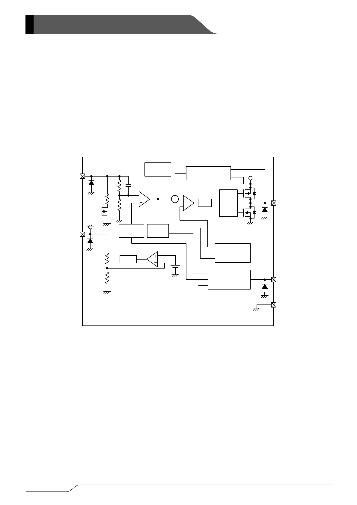
■OPERATIONAL DESCRIPTION
The XC9244/XC9245 series consists of a reference voltage source, ramp wave circuit, error amplifier, PWM comparator, phase compensation
circuit, output voltage adjustment resistors, P-channel MOS driver transistor, N-channel MOS switching transistor for the synchronous switch,
current limiter circuit, UVLO circuit and others. (See the block diagram below.)
The series ICs compare, using the error amplifier, the voltage of the internal voltage reference source with the feedback voltage from the V
pin through split resistors, R1 and R2. Phase compensation is performed on the resulting error amplifier output, to input a signal to the PWM
comparator to determine the turn-on time during PWM operation. The PWM comparator compares, in terms of voltage level, the signal from the
error amplifier with the ramp wave from the ramp wave circuit, and delivers the resulting output to the buffer driver circuit to cause the Lx pin to
output a switching duty cycle. This process is continuously performed to ensure stable output voltage. The current feedback circuit monitors
the P-channel MOS driver transistor current for each switching operation, and modulates the error amplifier output signal to provide multiple
feedback signals. This enables a stable feedback loop even when a low ESR capacitor such as a ceramic capacitor is used ensuring stable
output voltage.
XC9244/XC9245 Series, Type A
VOUT
R1
CEB
IN
V
R2
Vref with
Soft Start,
CE
UVLO
R3
R4
<Reference Voltage Source>
The reference voltage source provides the reference voltage to ensure stable output voltage of the DC/DC converter.
<Ramp Wave Circuit>
The ramp wave circuit determines switching frequency. The frequency is fixed internally as1.2MHz. Clock pulses generated in this circuit are
used to produce ramp waveforms needed for PWM operation, and to synchronize all the internal circuits.
<Error Amplifier>
The error amplifier is designed to monitor output voltage. The amplifier compares the reference voltage with the feedback voltage divided by the
internal split resistors, R1 and R2. When a voltage lower than the reference voltage is fed back, the output voltage of the error amplifier
increases. The gain and frequency characteristics of the error amplifier output are fixed internally to deliver an optimized signal to the mixer.
The error amplifier output signal optimized in the mixer is modulated with the current feedback signal. This signal is delivered to the PWM
compatator.
C
FB
Error Amp.
UVLO Comparator
Phase
Compensation
PWM/PFM
Selector
Current Feedback
Current Limit
PWM
Comparator
CEB
Logic
Synch.
Buffer
Drive
Ramp Wave
Generator
OSC
CE
Control
Logic
Lx
CE
V
SS
OUT
8/24

XC9244/XC9245
Series
■OPERATIONAL DESCRIPTION (Continued)
<Current Limit>
The current limiter circuit of the XC9244/XC9245 series monitors the current flowing through the P-channel MOS driver transistor connected to
the Lx pin, and features a combination of the current limit mode and the operation suspension mode.
① When the driver current is greater than a specific level, the current limit function operates to turn off the pulses from the Lx pin at any given
timing.
② When the P-channel MOS driver transistor is turned off, the limiter circuit is then released from the current limit detection state.
③ At the next pulse, the P-channel MOS driver transistor is turned on. However, the P-channel MOS driver transistor is immediately turned off
in the case of an over current state.
④ When the over current state is eliminated, the IC resumes its normal operation.
The IC waits for the over current state to end by repeating the steps ① through ③. If an over current state continues for a few ms and the
above three steps are repeatedly performed, the IC performs the function of latching the OFF state of the P-channel MOS driver transistor,
and goes into operation suspension mode. Once the IC is in suspension mode, operations can be resumed by either turning the IC off via
the CE/MODE pin, or by restoring power to the V
pulse output is suspended; therefore, the internal circuitry remains in operation. The current limit of the XC9244/XC9245 series can be set
at 900mA at typical. Besides, care must be taken when laying out the PC Board, in order to prevent misoperation of the current limit mode.
Depending on the state of the PC Board, latch time may become longer and latch operation may not work. In order to avoid the effect of
noise, the board should be laid out so that input capacitors are placed as close to the IC as possible.
pin. The suspension mode does not mean a complete shutdown, but a state in which
IN
<UVLO Circuit>
When the V
caused by unstable operation of the internal circuitry. When the V
releasing the UVLO function, the IC performs the soft start function to initiate output startup operation. The soft start function operates even
when the V
but causes pulse output to be suspended; therefore, the internal circuitry remains in operation.
<PFM Switch Current> (*1)
In PFM control operation, until coil current reaches to a specified level (I
that the P-ch MOS driver transistor is kept on (t
t
= L×I
ON
< PFM Duty Limit > (*1)
In PFM control operation, the PFM duty limit (DTY
Therefore, under the condition that the duty increases (e.g. the condition that the step-down ratio is small), it’s possible for P-ch MOS driver
transistor to be turned off even when coil current doesn’t reach to I
(* 1) XC9244 series exclude.
voltage becomes 1.6V or lower, the P-ch MOS driver transistor output driver transistor is forced OFF to prevent false pulse output
IN
pin voltage falls momentarily below the UVLO operating voltage. The UVLO circuit does not cause a complete shutdown of the IC,
IN
) can be given by the following formula.
ON
) is set to 300% (MAX.).
LIMIT_PFM
PFM
/ (V
-
V
) →I
IN
OUT
PFM
①
pin voltage becomes 2.25V or higher, switching operation takes place. By
IN
), the IC keeps the P-ch MOS driver transistor on. In this case, time
PFM
. →I
PFM
②
PFM
9/24

XC9244/XC9245 Series
■OPERATIONAL DESCRIPTION (Continued)
<CL High Speed Discharge>
XC9244/ XC9245 series can quickly discharge the electric charge at the output capacitor (C
whole IC circuit put into OFF state, is inputted via the N-ch MOS switch transistor located between the V
disabled, electric charge at the output capacitor (C
output capacitor (C
resistance value [R
N-channel transistor is calculated by the following formulas.
V = V
V: Output voltage after discharge
V
OUT(E)
t: Discharge time
τ: C
C
L
R
DCHG
×e
OUT(E)
: Output voltage
L×RDCHG
: Capacitance of Output capacitor
: CL auto-discharge resistance
) is set by the CL auto-discharge resistance (R) and the output capacitor (CL). By setting time constant of a CL auto-discharge
L
] and an output capacitor value (CL) as τ(τ= CL×R
DCHG
-t /
τ
or t = τln (V
OUT(E)
/V)
) is quickly discharged so that it may avoid application malfunction. Discharge time of the
L
), discharge time of the output voltage after discharge via the
DCHG
Output Voltage (Relative Value)
<CE Pin Function>
The operation of the XC9244/XC9245 series will enter into the shut down mode when a low level signal is input to the CE pin. During the
shutdown mode, the current consumption of the IC becomes 0μA (TYP.), with a state of high impedance at the Lx pin and C
discharge at V
sink current is 0μA (TYP.).
pin. The IC starts its operation by inputting a high level signal to the CE pin. The input to the CE pin is a CMOS input and the
OUT
1) XC9244/XC9245 series - Examples of how to use CE pin
(A)
) when a low signal to the CE pin which enables a
L
pin and the VSS pin. When the IC is
OUT
Output Voltage Disc hage Characteristics
R
100
90
80
70
60
50
40
30
100 = Setting Voltage Value
20
10
0
0 1020304050
Discharge Time t (ms)
SW_CE
ON
OFF
STATUS
Stand-by
Operation
=120Ω(TYP)
DCHG
CL=1 0μF
CL=2 0μF
CL=5 0μF
L
high speed
(B)
SW_CE STATUS
ON
OFF
Stand-by
Operation
<Soft Start>
The XC9244/ XC9245 series provide 0.25ms (TYP). Soft start time is defined as the time interval to reach 90% of the output voltage from the
time when the V
is turned on.
CE
10/24

XC9244/XC9245
Series
■NOTE ON USE
1. Please use this IC within the stated maximum ratings. For temporary, transitional voltage drop or voltage rising phenomenon, the IC is liable
to malfunction should the ratings be exceeded.
2. Spike noise and ripple voltage arise in a switching regulator as with a DC/DC converter. These are greatly influenced by external component
selection, such as the coil inductance, capacitance values, and board layout of external components. Once the design has been completed,
verification with actual components should be done.
3. When the difference between V
cycles may be skipped completely.
4. When the difference between V
that some cycles may be skipped completely.
and V
IN
and V
IN
is large in PWM control, very narrow pulses will be outputted, and there is the possibility that some
OUT
is small, and the load current is heavy, very wide pulses will be outputted and there is the possibility
OUT
V
:100mV/div
OUT
ILx:100mA/div
VLx:5V/div
5. With the IC, the peak current of the coil is controlled by the current limit circuit. Since the peak current increases when dropout voltage or load
current is high, current limit starts operation, and this can lead to instability. When peak current becomes high, please adjust the coil
inductance value and fully check the circuit operation. In addition, please calculate the peak current according to the following formula:
- V
Ipk = (V
L: Coil Inductance Value
f
6. When the peak current which exceeds limit current flows within the specified time, the built-in P-ch MOS driver transistor turns off. During the
time until it detects limit current and before the built-in transistor can be turned off, the current for limit current flows; therefore, care must be
taken when selecting the rating for the external components such as a coil.
7. Care must be taken when laying out the PC Board, in order to prevent misoperation of the current limit mode. Depending on the state of the
PC Board, latch time may become longer and latch operation may not work. In order to avoid the effect of noise, the board should be laid out
so that input capacitors are placed as close to the IC as possible.
8. Please do not use the IC at voltages below the recommended voltage range.
9. This IC should be used within the stated absolute maximum ratings in order to prevent damage to the device.
10.
11. The current limit is set to 1200mA (MAX.) at typical. However, the current of 1200mA or more may flow. In case that the current limit
OSC
When the IC is used in high temperature, output voltage may increase up to input voltage level at no load because of the leak current of the driver transistor.
functions while the V
occur at both ends of a coil. For this, the time rate of coil current becomes large. By contrast, when N-ch MOS driver transistor is ON,
there is almost no potential difference at both ends of the coil since the V
coil current becomes quite small. According to the repetition of this operation, and the delay time of the circuit, coil current will be converged
on a certain current value, exceeding the amount of current, which is supposed to be limited originally. Even in this case, however, after the
over current state continues for several ms, the circuit will be latched. A coil should be used within the stated absolute maximum rating in
order to prevent damage to the device.
)×OnDuty / (2×L×f
IN
OUT
: Oscillation Frequency
pin is shorted to the GND pin, when P-ch MOS driver transistor is ON, the potential difference for input voltage will
OUT
①Current flows into P-ch MOS driver transistor to reach the current limit (I
The current of I
②
③Because of no potential difference at both ends of the coil, the time rate of coil current becomes quite small.
④Lx oscillates very narrow pulses by the current limit for several ms.
⑤The circuit is latched, stopping its operation.
or more flows since the delay time of the circuit occurs during from the detection of the current limit to OFF of P-ch MOS driver transistor.
LIM
OSC
) + I
OUT
pin is shorted to the GND pin. Consequently, the time rate of
OUT
).
LIM
Horizon:200μsec/div
11/24

XC9244/XC9245 Series
■NOTE ON USE (Continued)
12. In order to stabilize VIN’s voltage level, we recommend that a by-pass capacitor (CIN) be connected as close as possible to the VIN & VSS pins.
13. In case of V
14. Torex places an importance on improving our products and their reliability.
We request that users incorporate fail-safe designs and post-aging protection treatment when using Torex products in their systems.
●Instructions of pattern layouts
1. In order to stabilize V
2. Please mount each external component as close to the IC as possible.
3. Wire external components as close to the IC as possible and use thick, short connecting traces to reduce the circuit impedance.
4. Make sure that the PCB GND traces are as thick as possible, as variations in ground potential caused by high ground currents at the time of
switching may result in instability of the IC.
5. This series’ internal P-ch driver transistors bring on heat because of the output current and ON resistance of driver transistors.
●Recommended Pattern Layout
st
1
Layer 2nd Layer
PCB
<2.5V, the maximum load current may be decreased less than 400mA due to the characteristics of current limit.
IN
voltage level, we recommend that a by-pass capacitor (CIN) be connected as close as possible to the VIN & VSS pins.
IN
12/24

■TEST CIRCUITS
XC9244/XC9245
Series
13/24

XC9244/XC9245 Series
■TYPICAL PERFORMANCE CHARACTERISTICS
(1) Efficiency vs. Output Current (Compare to different coil)
(1)
(1) Efficiency vs. Output Current
(1)
-
効率
Efficiency : EFFI (%)
効率
出力電流特性例(コイル別比較)
CIN=4.7μF(LMK212BJ475) CIN=4.7μF(LMK212BJ475)
100
80
60
40
20
0
0.1 1 10 100 1000
-
出力電流特性例
L=4.7μH,C
SPM3012(TDK)
NR3015(TAIYO YUDEN)
EPL3015(Coilcraft)
Output Current : I
=10μF(LMK212BJ106) L=4.7μH,CL=10μF(LMK212BJ106)
L
(mA)
OUT
XC9244/XC9245A12C XC9244/XC9245A18C
CIN=4.7μF(LMK212BJ475) CIN=4.7μF(LMK212BJ475)
L=4.7μH(SPM3012),C
100
VIN=2.3V
80
60
40
Efficiency : EFFI (%)
20
0
0.1 1 10 100 1000
4.2V
3.6V
Output Current : I
=10μF(LMK212BJ106) L=4.7μH(SPM3012),CL=10μF(LMK212BJ106)
L
PWM Control
=2.3V
V
IN
3.6V
4.2V
(mA)
OUT
XC9244/XC9245A33C XC9244/XC9245A12C
CIN=4.7μF(LMK212BJ475) CIN=4.7μF(LMK212BJ475)
L=4.7μH(SPM3012),C
100
80
60
VIN=4.2V
40
VIN=5.0V
Efficiency : EFFI (%)
20
0
0.1 1 10 100 1000
Output Current : I
=10μF(LMK212BJ106) L=4.7μH(SPM3012),CL=10μF(LMK212BJ106)
L
PWM Control
V
=4.2V
IN
5.0V
(mA)
OUT
XC9245A12C(VIN=3.6V)XC9244A12C(VIN=3.6V)
100
80
60
40
Efficiency : EFFI (%)
20
0
0.1 1 10 100 1000
100
80
60
40
Efficiency : EFFI (%)
20
0
(2) Output Voltage vs. Output Current
(2)
出力電圧- 出力電流特性例
1.30
1.28
(V)
1.25
OUT
1.23
1.20
1.18
1.15
Output Voltage : V
1.13
1.10
SPM3012(TDK)
NR3015(TAIYO YUDEN)
EPL3015(Coilcraft)
Output Current : I
4.2V
3.6V
0.1 1 10 100 1000
Output Current : I
VIN=2.3V,3.6V,4.2V
0.1 1 10 100 1000
Output Current : I
(mA)
OUT
PWM Control
=3.6V
V
IN
4.2V
(mA)
OUT
(mA)
OUT
14/24

XC9244/XC9245
■TYPICAL PERFORMANCE CHARACTERISTICS (Continued)
(2) Output Voltage vs. Output Current (Continued)
(2)
出力電圧
1.90
1.88
(V)
1.85
OUT
1.83
1.80
1.78
1.75
Output Voltage : V
1.73
1.70
-
出力電流特性例
XC9244/XC9245A18C XC9244/XC9245A33C
CIN=4.7μF(LMK212BJ475) CIN=4.7μF(LMK212BJ475)
L=4.7μH(SPM3012),C
VIN=3.6V,4.2V
0.1 1 10 100 1000
Output Current : I
=10μF(LMK212BJ106) L=4.7μH(SPM3012),CL=10μF(LMK212BJ106)
L
(mA)
OUT
3.40
3.38
(V)
3.35
OUT
3.33
3.30
3.28
3.25
Output Voltage : V
3.23
3.20
0.1 1 10 100 1000
VIN=4.2V,5.0V
Output Current : I
OUT
(mA)
(3) Ripple Voltage vs. Output Current
(3)
リップル電圧
L=4.7μH(SPM3012),C
100
80
60
V
40
-
出力電流特性例
XC9244/XC9245A12C XC9244/XC9245A18C
CIN=4.7μF(LMK212BJ475) CIN=4.7μF(LMK212BJ475)
=10μF(LMK212BJ106) L=4.7μH(SPM3012),CL=10μF(LMK212BJ106)
PWM Control
=2.3V,3.6V,4.2V
IN
L
PWM/PFM Automatic
Switching Control
=2.3V
V
IN
3.6V
4.2V
100
80
60
40
PWM Control
=3.6V,4.2V
V
IN
PWM/PFM Automatic
Switching Control
= 3.6V
V
IN
4.2V
20
Ripple Voltage : Vr (mV)
0
0.1 1 10 100 1000
20
Ripple Voltage : Vr (mV)
0
0.1 1 10 100 1000
Output Current : I
OUT
(mA)
Output Current : I
OUT
(mA)
(4) Output Voltage vs. Ambient Temperature
(4)
100
Ripple Voltage : Vr (mV)
XC9244/XC9245A33C
CIN=4.7μF(LMK212BJ475) CIN=4.7μF(LMK212BJ475)
L=4.7μH(SPM3012),C
80
60
PWM Control
=4.2V,5.0V
V
IN
40
20
0
0.1 1 10 100 1000
Output Current : I
=10μF(LMK212BJ106) L=4.7μH(SPM3012),CL=10μF(LMK212BJ106)
L
PWM/PFM Automatic
Switching Control
=4.2V
V
IN
5.0V
(mA)
OUT
出力電圧- 周囲温度特性例
1.98
1.94
1.90
(V)
out
1.86
1.82
1.78
1.74
1.70
Output Voltage :V
1.66
1.62
-50 -25 0 25 50 75 100
VIN=2.3V,3.6V,5.0V
Ambient temperture: Ta (℃)
Series
15/24

XC9244/XC9245 Series
■TYPICAL PERFORMANCE CHARACTERISTICS (Continued)
(5) Oscillation Frequency vs. Ambient Temperature (6) Oscillation Frequency vs. Input Voltage
(5)
発振周波数
1.5
1.4
(MHz)
OSC
1.3
1.2
1.1
1.0
0.9
Oscillation Freqency : f
0.8
-50 -25 0 25 50 75 100
(7) Quiescent Current vs. Ambient Temperature (8) Quiescent Current vs. Input Voltage
(7)
消費電流
40
35
30
25
20
15
10
5
Quiescent Current : Iq (μA)
0
-50 -25 0 25 50 75 100
(9) CE "H" Voltage vs. Ambient Temperature (10) CE "H" Voltage vs. Input Voltage
(9)CE"H"
1.0
0.9
0.8
(V)
0.7
CEH
0.6
0.5
0.4
0.3
0.2
CE"H" Voltage : V
0.1
0.0
-50 -25 0 25 50 75 100
-
周囲温度特性例
CIN=4.7μF(LMK212BJ475) CIN=4.7μF(LMK212BJ475)
L=4.7μH(SPM3012),C
VIN=3.6V
VIN=5.0V
Ambient temperture: Ta (℃)
-
周囲温度特性例
VIN=2.3V,3.6V,5.0V
Ambient temperture: Ta (℃)
-
電圧
周囲温度特性例
VIN=2.3V
VIN=3.6V
Ambient temperture: Ta (℃)
(6)
発振周波数- 入力電圧特性例
=10μF(LMK212BJ106) L=4.7μH(SPM3012),CL=10μF(LMK212BJ106)
L
VIN=2.3V
VIN=5.0V
1.5
1.4
(MHz)
OSC
1.3
1.2
1.1
1.0
0.9
Oscillation Freqency : f
0.8
1.5 2.5 3.5 4.5 5.5 6.5
(8)
消費電流- 入力電圧特性例
40
35
30
25
20
15
10
5
Quiescent Current : Iq (μA)
0
1.5 2.5 3.5 4.5 5.5 6.5
(10)CE"H"
1.0
0.9
0.8
(V)
0.7
CEH
0.6
0.5
0.4
0.3
0.2
CE"H" Voltage : V
0.1
0.0
1.5 2.5 3.5 4.5 5.5 6.5
電圧
Ta=-40
Ta=25℃,85
Ta=-40
Input Voltage: V
Ta=-40
Input Voltage: V
-
入力電圧特性例
℃
Ta=25
Input Voltage: V
℃
℃
Ta=25℃,85
℃
℃
(V)
IN
(V)
IN
Ta=85
(V)
IN
℃
℃
16/24

XC9244/XC9245
■TYPICAL PERFORMANCE CHARACTERISTICS (Continued)
(11) Lx SW "H" ON Resistance vs. Ambient Temperature (12) Lx SW "H" ON Resistance vs. Input Voltage
(11)Lx SW "H"ON
抵抗
-
周囲温度特性例
(12)Lx SW "H"ON
抵抗- 入力電圧特性例
1.6
(Ω)
1.4
LxH
1.2
1.0
0.8
0.6
0.4
0.2
0.0
Lx SW "H"ON Resistance : R
-50 -25 0 25 50 75 100
VIN=2.3V
VIN=3.6V
VIN=5.0V
Ambient temperture: Ta (℃)
1.6
(Ω)
1.4
LxH
1.2
1.0
0.8
0.6
0.4
℃
0.2
0.0
Lx SW "H"ON Resistance : R
Ta=-40
1.5 2.5 3.5 4.5 5.5 6.5
Input Voltage: V
Ta=25
℃
Ta=85
(V)
IN
℃
(13) Lx SW "L" ON Resistance vs. Ambient Temperature (14) Lx SW "L" ON Resistance vs. Input Voltage
(13)Lx SW "L"ON
抵抗
-
周囲温度特性例
(14)"Lx SW "L"ON
抵抗- 入力電圧特性例
1.6
(Ω)
1.4
LxL
1.2
1.0
Lx SW "L"ON Resistance : R
0.8
0.6
0.4
0.2
0.0
VIN=2.3V
-50 -25 0 25 50 75 100
Ambient temperture: Ta (℃)
VIN=3.6V
VIN=5.0V
1.6
(Ω)
1.4
LxL
1.2
1.0
0.8
0.6
0.4
0.2
0.0
Lx SW "L"ON Resistance : R
1.5 2.5 3.5 4.5 5.5 6.5
℃
Ta=-40
Input Voltage: V
Ta=25
℃
IN
Ta=85
(V)
(15) CL Discharge vs. Ambient Temperature (16) CL Discharge vs. Input Voltage
(15)C
放電抵抗
L
-
周囲温度特性例
(16)C
放電抵抗- 入力電圧特性例
L
300
250
(Ω)
200
DCHG
150
100
Discharge : R
L
50
C
0
-50 -25 0 25 50 75 100
VIN=3.6V,5.0V
VIN=2.3V
300
250
(Ω)
200
DCHG
150
100
Discharge : R
L
50
C
0
1.5 2.5 3.5 4.5 5.5 6.5
Ta=25
℃
Ta=85
Ta=-40
℃
Ambient temperture: Ta (℃)
Input Voltage: V
IN
(V)
Series
℃
℃
17/24

XC9244/XC9245 Series
■TYPICAL PERFORMANCE CHARACTERISTICS (Continued)
(17) PFM Switch Current vs. Ambient Temperature (18) PFM Switch Current vs. Input Voltage
(17)PFM
スイッチ電流- 周囲温度特性例
V
=0.8V,CIN=4.7μF(LMK212BJ475) V
250
230
(mA)
210
PFM
190
170
150
130
110
90
70
PFM Switch Current : I
50
-50 -25 0 25 50 75 100
OUT(E)
L=4.7μH(SPM3012),C
VIN=3.6V
Ambient temperture: Ta (℃)
=10μF(LMK212BJ106) L=4.7μH(SPM3012),CL=10μF(LMK212BJ106)
L
VIN=2.3V
VIN=5.0V
(19) Current Limit vs. Ambient Temperature (20) Current Limit vs. Input Voltage
(19)
電流制限
-
周囲温度特性例
1200
1100
1000
(mA)
LIM
900
800
700
600
Current Limit : I
500
400
VIN=2.3V
-50 -25 0 25 50 75 100
VIN=3.6V
Ambient temperture: Ta (℃)
VIN=5.0V
(21) UVLO Voltage vs. Ambient Temperature (22) Soft Start Time vs. Input Voltage
(21)UVLO
電圧
-
周囲温度特性例
2.3
2.2
2.1
2.0
1.9
1.8
1.7
1.6
UVLO Voltage : UVLO (V)
1.5
-50 -25 0 25 50 75 100
Ambient temperture: Ta (℃)
(18)PFM
(mA)
PFM
PFM Switch Current : I
(20)
1200
1100
1000
(mA)
LIM
Current Limit : I
(22)
(μs)
SS
Soft Start Time: t
スイッチ電流- 入力電圧特性例
=0.8V,CIN=4.7μF(LMK212BJ475)
OUT(E)
250
230
210
190
170
150
130
110
90
70
50
1.5 2.5 3.5 4.5 5.5 6.5
℃
Ta=25
Input Voltage: V
Ta=-40
Ta=85
IN
℃
(V)
電流制限- 入力電圧特性例
Ta=85
900
800
700
600
500
400
1.5 2.5 3.5 4.5 5.5 6.5
Input Voltage: V
Ta=25
℃
IN
Ta=-40
(V)
ソフトスタート時間- 周囲温度特性例
CIN=4.7μF(LMK212BJ475)
L=4.7μH(SPM3012),C
500
450
400
350
300
250
200
150
100
50
V
=2.0V
OUT
V
OUT
0
-50 -25 0 25 50 75 100
Ambient temperture: Ta (℃)
=10μF(LMK212BJ106)
L
V
=4.0V
OUT
=0.8V
℃
℃
℃
18/24

XC9244/XC9245
■TYPICAL PERFORMANCE CHARACTERISTICS (Continued)
(23) Rise Wave Form
(23)
起動波形例
XC9244/XC9245A12C XC9244/XC9245A18C
CIN=4.7μF(LMK212BJ475) CIN=4.7μF(LMK212BJ475)
L=4.7μH(SPM3012),C
VIN=5.0V
=1mA
I
OUT
=10μF(LMK212BJ106) L=4.7μH(SPM3012),CL=10μF(LMK212BJ106)
L
VIN=5.0V
=1mA
I
OUT
V
:0.5V/div
OUT
V
OUT
:0.5V/div
CE :0V⇒5.0V
CE :0V⇒5.0V
100μs/div
100μs/div
V
XC9244/XC9245A33C
L=4.7μH(SPM3012),C
VIN=5.0V
=1mA
I
OUT
:1.0V/div
OUT
C
=4.7μF(LMK212BJ475)
IN
=10μF(LMK212BJ106)
L
CE :0V⇒5.0V
100μs/div
Series
19/24

XC9244/XC9245 Series
■TYPICAL PERFORMANCE CHARACTERISTICS (Continued)
(24) Load Transient Response
(24)
負荷過渡応答特性例
V
:50mV/div V
OUT
V
:50mV/div V
OUT
XC9244A18C
CIN=4.7μF(LMK212BJ475) CIN=4.7μF(LMK212BJ475)
L=4.7μH(SPM3012),C
XC9244A18C
C
L=4.7μH(SPM3012),C
XC9244A18C
=10μF(LMK212BJ106) L=4.7μH(SPM3012),CL=10μF(LMK212BJ106)
L
I
=1mA⇒100mA
OUT
:50mV/div
50μs/div
=4.7μF(LMK212BJ475) CIN=4.7μF(LMK212BJ475)
IN
=10μF(LMK212BJ106) L=4.7μH(SPM3012),CL=10μF(LMK212BJ106)
L
I
=100mA⇒1mA
OUT
200μs/div
OUT
:50mV/div
OUT
XC9244A18C
I
=1mA⇒300mA
OUT
I
=300mA⇒1mA
OUT
200μs/div
50μs/div
20/24

XC9244/XC9245
■TYPICAL PERFORMANCE CHARACTERISTICS (Continued)
(24) Load Transient Response (Continued)
(24)
負荷過渡応答特性例
XC9245A18C XC9245A18C
CIN=4.7μF(LMK212BJ475) CIN=4.7μF(LMK212BJ475)
L=4.7μH(SPM3012),C
=10μF(LMK212BJ106) L=4.7μH(SPM3012),CL=10μF(LMK212BJ106)
L
I
=1mA⇒100mA
OUT
I
=1mA⇒300mA
OUT
V
:50mV/div
OUT
V
:50mV/div
50μs/div 50μs/div
OUT
XC9245A18C XC9245A18C
=4.7μF(LMK212BJ475) CIN=4.7μF(LMK212BJ475)
C
IN
L=4.7μH(SPM3012),C
=10μF(LMK212BJ106) L=4.7μH(SPM3012),CL=10μF(LMK212BJ106)
L
I
=100mA⇒1mA
OUT
I
=300mA⇒1mA
OUT
V
V
:50mV/div
OUT
:50mV/div
OUT
200μs/div
200μs/div
Series
21/24

XC9244/XC9245 Series
■PACKAGING INFORMATION
●USPN-6
●USPN-6 Reference Pattern Layout ●USPN-6 Reference Metal Mask Design
0.25 0.2 0.25
6
5
4
1
2
0.15 0.45 0.45 0.15
3
0.2 0.2 0.2
6
5
4
1
2
0.1 0.45 0.45 0.1
3
22/24

■MARKING RULE
XC9244 Series
●USPN-6
1
2
3
③ ④
①
②
6
5
4
① represents product series and output voltage
MARK
A
B
C
C
XC9245 Series
MARK
D
E
F
F
② represents product function
MARK OUTPUT VOLTAGE MARK OUTPUT VOLTAGE
0 0.8 0.85 F 2.3 2.35
1 0.9 0.95 H 2.4 2.45
2 1.0 1.05 K 2.5 2.55
3 1.1 1.15 L 2.6 2.65
4 1.2 1.25 M 2.7 2.75
5 1.3 1.35 N 2.8 2.85
6 1.4 1.45 P 2.9 2.95
7 1.5 1.55 R 3.0 3.05
8 1.6 1.65 S 3.1 3.15
9 1.7 1.75 T 3.2 3.25
A 1.8 1.85 3.8 U 3.3 3.35
B 1.9 1.95 3.9 V 3.4 3.45
C 2.0 2.05 4.0 X 3.5 3.55
D 2.1 2.15 3.85 Y 3.6 3.65
E 0.8 0.85 3.95 Z 3.7 3.75
③④ represents production lot number
01 to 09, 0A to 0Z, 11 to 9Z, AA to AZ, B1 to ZZ repeated.
(G, I, J, O, Q, W excluded)
*No character inversion used.
OUTPUT
VOLTAGE
0.8~3.7
0.85~3.75
3.8~4.0
3.85~3.95
OUTPUT
VOLTAGE
0.8~3.7
0.85~3.75
3.8~4.0
3.85~3.95
VOLTAGE
INCREMENT
0.1
0.05
0.1
0.05
VOLTAGE
INCREMENT
0.1
0.05
0.1
0.05
XC9244/XC9245
Series
PRODUCT SERIES
XC9244A08C**-G ~ XC9244A37C**-G
XC9244A0LC**-G ~ XC9244A3KC**-G
XC9244A38C**-G ~ XC9244A40C**-G
XC9244A3LC**-G ~ XC9244A3MC**-G
PRODUCT SERIES
XC9245A08C**-G ~ XC9245A37C**-G
XC9245A0LC**-G ~ XC9245A3KC**-G
XC9245A38C**-G ~ XC9245A40C**-G
XC9245A3LC**-G ~ XC9245A3MC**-G
23/24

XC9244/XC9245 Series
24/24
1. The products and product specifications contained herein are subject to change without
notice to improve performance characteristics. Consult us, or our representatives
before use, to confirm that the information in this datasheet is up to date.
2. We assume no responsibility for any infringement of patents, patent rights, or other
rights arising from the use of any information and circuitry in this datasheet.
3. Please ensure suitable shipping controls (including fail-safe designs and aging
protection) are in force for equipment employing products listed in this datasheet.
4. The products in this datasheet are not developed, designed, or approved for use with
such equipment whose failure of malfunction can be reasonably expected to directly
endanger the life of, or cause significant injury to, the user.
(e.g. Atomic energy; aerospace; transport; combustion and associated safety
equipment thereof.)
5. Please use the products listed in this datasheet within the specified ranges.
Should you wish to use the products under conditions exceeding the specifications,
please consult us or our representatives.
6. We assume no responsibility for damage or loss due to abnormal use.
7. All rights reserved. No part of this datasheet may be copied or reproduced without the
prior permission of TOREX SEMICONDUCTOR LTD.
 Loading...