


)
)
F
XC9242/XC9243 Series
2A Synchronous Step-Down DC/DC Converters
■GENERAL DESCRIPTION
The XC9242/XC9243 series is a group of synchronous-rectification step-down DC/DC converters with a built-in 0.11Ω
(TYP.) P-channel MOS driver transistor and 0.12Ω(TYP.) N-channel MOS switching transistor, designed to allow the use of
ceramic capacitors. The small on-resistances of these two internal driver transistors enable a high efficiency, stable power
supply with an output current up to 2A. The XC9242/XC9243 series has operating voltage range of 2.7V~6.0V and a 0.8V
(±2.0%) reference voltage, and using externally connected resistors, the output voltage can be set freely from 0.9V. With
an internal switching frequency of 1.2MHz or 2.4MHz, small external components can be used.
The XC9242 series is PWM control, and the XC9243 series is PWM/PFM, which automatically switches from PWM to PFM
during light loads and provides high efficiency, high load response, low voltage ripple, can be achieved over a wide range of
load conditions. The series have a high speed soft-start as fast as 1ms in typical for quick turn-on. It’s suitable for
large-current application due to limit current is configured 4.0A in typical. During stand-by, all circuits are shutdown to
reduce current consumption to as low as 1.0μA or less. The integrated C
charge at the output capacitor C
Due to C
Lock Out) function, the internal P-channel driver transistor is forced OFF when input voltage becomes 2.5V or lower. The
series are available in USP-10B package.
■APPLICATIONS
● Mobile phones
● Bluetooth headsets
● Personal digital assistance
● Portable game consoles
● Digital still cameras, Camcorders
■TYPICAL APPLICATION CIRCUIT
discharge function, malfunction on LX is prevented when Stand-by mode. With the built-in UVLO (Under Voltage
L
●XC9242/XC9243 Series (FB Type)
to be discharged via the internal discharge switch located between the LX and VSSpins.
L
■FEATURES
Driver Transistor : 0.11Ω P-ch Driver Transistor
0.12Ω N-ch Switching Transistor
Input Voltage Range : 2.7V~6.0V
Output Voltage Setting : 0.9V~V
FB Voltage : 0.8V±2.0%
High Efficiency : 95%(TYP.)*
Output Current : 2.0A
Oscillation Frequency : 1.2MHz±15%, 2.4MHz±15%
Maximum Duty Cycle : 100%
Functions : Soft-Start Circuit Built-In
C
Thermal Shutdown
UVLO
Output Capacitor : Low ESR Ceramic Capacitor
Control Methods : PWM control (XC9242)
PWM/PFM Auto (XC9243)
Operating Ambient Temperature
Package : USP-10B
Environmentally Friendly
* Performance depends on external components and wiring on the PCB.
■TYPICAL PERFORMANCE
CHARACTERISTICS
●Efficiency vs. Output Current (fosc=1.2MHz, V
discharge function which enables the electric
L
100
90
80
70
60
50
40
30
Efficiency: EFFI (%)
20
10
0
0.1 1 10 100 1000 10000
☆GreenOperation Compatible
IN
Discharge
L
Current Limit Circuit(automatic return
: -40℃ ~ +85℃
: EU RoHS Compliant, Pb Free
XC9242B08C
L=4.7μH(SLF7055),C
C
=1μF(LMK107BJ105KAx1),CL=20μF(LMK212ABJ106KGx2
IN2
Output Current: I
OUT
IN1
R
=47kΩ, R
VIN=5.0V
(mA)
ETR0521-005
=3.3V)
OUT
=20μF(LMK212ABJ106KGx2
=15kΩ, C
=330p
1/27
)

XC9242/XC9243 Series
■ BLOCK DIAGRAM
●XC9242/XC9243 Series
* Diodes inside the circuits are ESD protection diodes and parasitic diodes.
■ PRODUCT CLASSIFICATION
●Ordering Information
XC9242①②③④⑤⑥-⑦
XC9243①②③④⑤⑥-⑦
DESIGNATOR ITEM SYMBOL DESCRIPTION
①
②③
④
⑤⑥-⑦
(*1) The “-G” suffix indicates that the products are Halogen and Antimony free as well as being fully RoHS compliant.
(*2) The XC9242/XC9243 reels are shipped in a moisture-proof packing.
Selection Guide
TYPE
B Fixed Yes Yes Yes Yes Yes
(*1)
Fixed PWM control
(*1)
PWM / PFM automatic switching control
(*1)
SOFT-START
TIME
Functional Selection
Output Voltage
Oscillation Frequency
Package (Order Unit) DR-G USP-10B (3,000/Reel)
CHIP
ENABLE
CURRENT
LIMITER
B C
08 Reference Voltage is fixed at 0.8V
C 1.2MHz
D 2.4MHz
THERMAL
SHUTDOWN
UVLO
Discharge
L
CL AUTO-
DISCHARGE
(*2)
2/27

■ PIN CONFIGURATION
XC9242/XC9243
Series
* Please connect the power input and analog input pins when operating.
* Please connect the two Lx pins (No.1 and 10).
* Please connect the power ground pins (No.2 and 3) and analog ground pin (No.5) when operating.
*It is recommended that the heat dissipation pad of the USP-10B package is soldered by using the reference mount
pattern and metal mask pattern for mounting strength. The mount pattern should be electrically opened or
connected to AGND pin (No.5) and PGND pin (No.2, and 3).
■ PIN ASSIGNMENT
PIN NUMBER
USP-10B
8,9 PVIN Power Input
7 AVIN Analog Input
2,3 PGND Power Ground
5 AGND Analog Ground
6 CE Chip Enable
4 FB Output Voltage Monitor
1,10 LX Switching Output
■ CE PIN FUNCTION
PIN NAME SIGNAL STATUS
XC9242/9243 Series
PIN NAME FUNCTION
CE
* Please do not leave the CE pin open.
H Active
L Stand-by
3/27

XC9242/XC9243 Series
■ ABSOLUTE MAXIMUM RATINGS
Ta=25℃
PAR AMET ER SYMBOL RATINGS UNIT
PVIN Pin Voltage V
AVIN Pin Voltage V
CE Pin Voltage VCE -0.3 ~ +7.0 V
FB Pin Voltage VFB -0.3 ~ +7.0 V
Lx Pin Voltage VLx -0.3 ~ +7.0 or V
Lx Pin Current ILx
Power Dissipation USP-10B Pd 150 mW
Operating Ambient
Temperature
Storage Temperature T
* All voltages are described based on the ground voltage of AGND and PGND.
(*1) Please connect PVIN pin and AVIN pin for use.
(*2) The maximum value should be either +7.0 or V
(*3) It is measured when the two Lx pins (No.1 and 10) are tied up to each other.
PVIN
AVI N
-0.3 ~ +7.0
PVIN
(*3)
±6.0
Topr -40 ~ +85
-55 ~ +125
stg
+0.3 in the lowest.
PVIN
(*1)
V
(*2)
+0.3
V
A
℃
℃
4/27

XC9242/XC9243
■ ELECTRICAL CHARACTERISTICS
●XC9242/XC9243, f
PARAMETER SYMBOL CONDITIONS MIN TYP. MAX. UNIT CIRCUIT
FB Voltage VFB
Operating Voltage Range
Maximum Output Current
UVLO Voltage V
Quiescent Current Iq V
Stand-by Current I
Oscillation Frequency
PFM Switch Current
PFM Duty Limit
Maximum Duty Limit D
Minimum Duty Limit D
Efficiency EFFI
LXSW”H”ON Resistance
LXSW”L”ON Resistance
LXSW”H” Leakage Current
Current Limit I
Output Voltage
Temperature
Characteristics
CE”H” Voltage V
CE”L” Voltage V
CE”H” Current I
CE”L” Current I
FB”H” Current I
FB”L” Current I
Soft-Start Time tSS
Thermal Shutdown
Temperature
Hysteresis Width T
CL Discharge R
NOTE:
External Components: C
Condition: Unless otherwise stated, ”H”=V
(*1) Mount conditions affect heat dissipation. Maximum output current is not guaranteed when T
(*2) When the difference between the input and the output is small, some cycles may be skipped completely before current maximizes.
If current is further pulled from this state, output voltage will decrease because of P-ch driver ON resistance.
(*3) These values include UVLO detect voltage, UVLO release voltage and hysteresis operating voltage range.
UVLO release voltage is defined as the V
(*4) XC9242 series exclude I
(*5) EFFI = { ( output voltage×output current ) / ( input voltage×input current) }×100
(*6) On resistance = (V
(*7) Design value
(*8) When temperature is high, a current of approximately 20μA (maximum) may leak.
(*9) Current limit denotes the level of detection at peak of coil current.
=1.2MHz, Ta=25℃
OSC
= 5.0V, VCE =5.0V
V
IN
Voltage to start oscillation while
=0.72V → 0.88V
V
FB
VIN When connected to external components 2.7 - 6.0 V ①
=5.0V
V
IN=VCE
When connected to external components
=5.0V, VFB=0.72V
V
CE
Voltage which Lx pin holding ”L” level
=5.0V, VFB=0.88V - 41 78 μA ②
IN=VCE
=5.0V, VCE=0V, VFB=0.88V - 0.01 1.00 μA ②
IN
=5.0V, I
V
IN=VCE
When connected to external components
=4.0V, I
V
IN=VCE
When connected to external components
VIN=VCE=2.7V, I
When connected to external components
=5.0V, I
V
IN=VCE
R
=47kΩ, R
FB1
=5.0V, VFB=0.72V
IN=VCE
I
=100mA
OUT
/
-40℃≦To pr ≦85℃
When connected to external components
=5.0V, VFB=0.72V Applied voltage to VCE
V
IN
Voltage changes Lx to “H” level
=5.0V, VFB=0.72V Applied to VCE Voltage
V
IN
changes Lx to “L” level
=5.0V, VCE=0V, VFB=0V -0.1 - 0.1 μA ⑤
IN
=5.0V, VCE=0V, VFB=5.0V -0.1 - 0.1 μA ⑤
IN
=5.0V, VCE=0V→5.0V, I
V
IN
(*4)
I
(*4)
DTY
(V
OUT
I
OUTMAX
UVLO
V
STB
f
OSC
PFM
LIMIT_PFM
VIN=VCE=5.0V, VFB=0.72V 100 - - % ③
MAX
VIN=VCE=5.0V, VFB=0.88V - - 0 % ③
MIN
R
VIN=VCE=4.0V, VFB=0.72V
LxH
R
- 0.12 0.30
LxL
I
VIN=5.0V, VCE=0V, VFB=0.88V, VLx=0V - 0.01 1.00
LeakH
V
LIM
ΔV
OUT
・Δtopr)
CEH
CEL
VIN=5.0V, VCE=5.0V, VFB=0V -0.1 - 0.1 μA ⑤
CEH
V
CEL
V
FBH
VIN=5.0V, VCE=0V, VFB=0V -0.1 - 0.1 μA ⑤
FBL
When connected to external components
- 150 - ℃ -
T
TSD
- 20 - ℃ -
HYS
VIN=5.0V, VCE=0V, VFB=0.72V, VLx=1.0V 80 130 160 Ω ⑥
DCHG
=20μF(ceramic), C
IN1
R
=15kΩ, R
FB1
PFM
– Lx pin measurement voltage) / 100mA
IN
=30kΩ, CFB=1000pF
FB2
and DTY
=1μF(ceramic), L=4.7μH(SLF7055T-4R7 TDK), CL=20μF(ceramic)
IN2
~ VIN - 1.2V, “L”=+ 0.1V ~ -0.1V
IN
voltage which makes Lx pin “H”.
IN
because those are only for the PFM control’s functions.
LIMIT_PFM
(*1,*2)
=300mA
OUT
=1mA
OUT
=1mA
OUT
=500mA
OUT
=15kΩ, CFB=330pF
FB2
(*5)
(*6)
(*9)
- 4.0 - A ④
OUT
0.784 0.800 0.816 V ③
2.0 - - A ①
(*3)
2.00 - 2.68 V ③
1020 1200 1380 kHz ①
- 280 - mA ①
- 180 250 % ①
- 95 - % ①
- 0.11 0.21 Ω ④
(*7)
Ω -
(*8)
μA ⑤
- ±100 - ppm/℃ ①
1.2 - V
V ③
IN
AGND - 0.4 V ③
=1mA
0.3 1.0 2.0 ms ①
starts to operate earlier.
TSD
Series
5/27

XC9242/XC9243 Series
■ ELECTRICAL CHARACTERISTICS (Continued)
XC9242/XC9243, f
PARAMETER SYMBOL CONDITIONS MIN. TYP. MAX. UNIT CIRCUIT
FB Voltage VFB
Operating Voltage Range
Maximum Output Current
UVLO Voltage V
Quiescent Current Iq V
Stand-by Current I
Oscillation Frequency
PFM Switch Current
PFM Duty Limit
Maximum Duty Limit D
Minimum Duty Limit D
Efficiency EFFI
LXSW”H”ON Resistance
LXSW”L”ON Resistance
LXSW”H” Leakage Current
Current Limit I
Output Voltage
Temperature
Characteristics
CE”H” Voltage V
CE”L” Voltage V
CE”H” Current I
CE”L” Current I
FB”H” Current I
FB”L” Current I
Soft-Start Time tSS
Thermal Shutdown
Temperature
Hysteresis Width T
CL Discharge R
NOTE:
External Components: C
R
Condition: Unless otherwise stated, ”H”= V
(*1) Mount conditions affect heat dissipation. Maximum output current is not guaranteed when T
(*2) When the difference between the input and the output is small, some cycles may be skipped completely before current maximizes.
If current is further pulled from this state, output voltage will decrease because of P-ch driver ON resistance.
(*3) These values include UVLO detect voltage, UVLO release voltage and hysteresis operating voltage range.
UVLO release voltage is defined as the V
(*4) XC9242 series exclude I
(*5) EFFI = { ( output voltage×output current ) / ( input voltage×input current) }×100
(*6) On resistance = (V
(*7) Design value
(*8) When temperature is high, a current of approximately 20μA (maximum) may leak.
(*9) Current limit denotes the level of detection at peak of coil current.
=2.4MHz, Ta=25℃
OSC
V
= VCE =5.0V
IN
Voltage to start oscillation while
=0.72V → 0.88V
V
FB
VIN When connected to external components 2.7 - 6.0 V ①
V
=5.0V
IN=VCE
When connected to external components
V
=5.0V, VFB=0.72V
CE
Voltage which Lx pin holding ”L” level
=5.0V, VFB=0.72V - 53 92 μA ②
IN=VCE
V
=5.0V, I
IN=VCE
When connected to external components
V
=6.0V, I
IN=VCE
When connected to external components
VIN=VCE=2.7V, I
When connected to external components
V
=5.0V, I
IN=VCE
=47kΩ, R
R
FB1
=5.0V, VFB=0.72V
IN=VCE
=100mA
I
OUT
-40℃≦To pr ≦85℃
When connected to external components
V
=5.0V, VFB=0.72V
IN
Applied voltage to VCE Voltage changes Lx to “H” level
V
=5.0V, VFB=0.72V
IN
Applied voltage to VCE Voltage changes Lx to “L” level
V
=5.0V, VCE=0V→5.0V, I
IN
(*4)
(*4)
DTY
I
OUTMAX
UVLO
VIN=5.0V, VCE=0V, VFB=0.88V - 0.01 1.00 μA ②
STB
f
OSC
I
PFM
LIMIT_PFM
VIN=VCE=5.0V, VFB=0.72V 100 - - % ③
MAX
VIN=VCE=5.0V, VFB=0.88V - - 0 % ③
MIN
R
VIN=VCE=4.0V, VFB=0.72V
LXH
R
- 0.12 0.30
LXL
I
VIN=5.0V, VCE=0V, VFB=0.88V, VLx=0V - 0.01 1.00
LeakH
V
LIM
Δ
V
/
OUT
・Δ
topr)
(V
OUT
CEH
CEL
VIN=5.0V, VCE=5.0V, VFB=0V -0.1 - 0.1 μA ⑤
CEH
VIN=5.0V, VCE=0V, VFB=0V -0.1 - 0.1 μA ⑤
CEL
VIN=5.0V,VCE=0V, VFB=5.0V -0.1 - 0.1 μA ⑤
FBH
VIN=5.0V,VCE=0V, VFB=0V -0.1 - 0.1 μA ⑤
FBL
When connected to external components
- 150 - ℃ -
T
TSD
- 20 - ℃ -
HYS
VIN=5.0V, VCE=0V, VFB=0.72V, VLx=1.0V 80 130 160 Ω ⑥
DCHG
=20μF(ceramic), C
IN1
=15kΩ, R
FB1
PFM
– Lx pin measurement voltage) / 100mA
IN
=30kΩ, CFB=1000pF
FB2
and DTY
=1μF(ceramic), L=2.2μH(SLF7055T-2R2 TDK), CL=20μF(ceramic)
IN2
~ VIN - 1.2V, “L”= + 0.1V ~ -0.1V
IN
voltage which makes Lx pin “H”.
IN
because those are only for the PFM control’s functions.
LIMIT_PFM
(*1,*2)
=1000mA
OUT
=1mA
OUT
=1mA
OUT
=500mA
OUT
=15kΩ, CFB=330pF
FB2
(*5)
(*6)
- 0.11 0.21 Ω ④
(*9)
- 4.0 - A ④
=1mA
OUT
0.784 0.800 0.816 V ③
2.0 - - A ①
(*3)
2.00 - 2.68 V ③
2040 2400 2760 kHz ①
- 680 - mA ①
- 180 250 % ①
- 95 - % ①
(*7)
Ω -
(*8)
μA ⑤
- ±100 - ppm/℃ ①
1.2 - VIN V ③
AGND - 0.4 V ③
0.3 1.0 2.0 ms ①
starts to operate earlier.
TSD
6/27

XC9242/XC9243
Series
■TYPICAL APPLICATION CIRCUIT
●XC9242/XC9243 Series
External Components
1.2MHz 2.4MHz
L:
C
:
20μF (LMK212ABJ106KG 10V/10μF x2)
IN1
C
1μF (LMK107BJ105KA 10V/1μF x1)
IN2
CL:
20μF (LMK212ABJ106KG 10V/10μF x2)
<Output Voltage Setting>
Output voltage can be set by adding external split resistors. Output voltage is determined by the following equation, based on the values of
RFB1 and RFB2. The sum of RFB1 and RFB2 should normally be 100kΩ or less. Output voltage range is 0.9V~5.5V by a 0.8V (±2.0%)
reference voltage. When input voltage (V
(V
).
IN
VOUT = 0.8 x (RFB1 + RFB2) / RFB2
The value of C
are required from 1kHz to 10kHz depending on the application, value of inductance (L), and value of load capacitance (C
[Example of calculation]
When R
When C
V
, speed-up capacitor for phase compensation, should be f
FB
=47kΩ, R
FB1
=330pF, fzfb= 1/(2
FB
R
OUT
FB1
(V) (kΩ) (kΩ) (pF) (V) (kΩ) (kΩ) (pF)
1.0 7.5 30 2000 2.5 51 24 300
1.2 15 30 1000 3.0 33 12 470
1.5 26 30 560 3.3 47 15 330
1.8 30 24 510 5.0 43 8.2 390
4.7μH(SLF7055T-4R7)
4.7μH(SPM6530T-4R7)
=15kΩ, V
FB2
R
=0.8×(47kΩ+15kΩ) / 15kΩ =3.3V
OUT
×π×
330pF×47 kΩ) =10.26kHz
CFB V
FB2
L:
C
:
20μF (LMK212ABJ106KG 10V/10μF x2)
IN1
C
IN2
CL:
20μF (LMK212ABJ106KG 10V/10μF x2)
) ≦setting output voltage, output voltage (V
IN
OUT
R
FB1
R
2.2μH(SLF7055T-2R2)
2.2μH(SPM6530T-2R2)
1μF (LMK107BJ105KA 10V/1μF x1)
= 1 / (2 x
ZFB
CFB
FB2
) can not output the power more than input voltage
OUT
π x
CFB x RFB1) which is equal to 10kHz. Adjustments
).
L
7/27

XC9242/XC9243 Series
■ OPERATIONAL DESCRIPTION
The XC9242/XC9243 series consists of a reference voltage source, ramp wave circuit, error amplifier, PWM comparator, phase
compensation circuit, output voltage adjustment resistors, P-channel MOS driver transistor, N-channel MOS switching transistor for the
synchronous switch, current limiter circuit, UVLO circuit and others. (See the block diagram above.) The series ICs compare, using the error
amplifier, the voltage of the internal voltage reference source with the feedback voltage from the FB pin. Phase compensation is performed on
the resulting error amplifier output, to input a signal to the PWM comparator to determine the turn-on time during PWM operation. The PWM
comparator compares, in terms of voltage level, the signal from the error amplifier with the ramp wave from the ramp wave circuit, and delivers
the resulting output to the buffer driver circuit to cause the Lx pin to output a switching duty cycle. This process is continuously performed to
ensure stable output voltage. The current feedback circuit monitors the P-channel MOS driver transistor current for each switching operation,
and modulates the error amplifier output signal to provide multiple feedback signals. This enables a stable feedback loop even when a low
ESR capacitor such as a ceramic capacitor is used ensuring stable output voltage.
<Reference Voltage Source>
The reference voltage source provides the reference voltage to ensure stable output voltage of the DC/DC converter.
<Ramp Wave Circuit>
The ramp wave circuit determines switching frequency. The frequency is fixed internally and can be selected from 1.2MHz or 2.4MHz.
Clock pulses generated in this circuit are used to produce ramp waveforms needed for PWM operation, and to synchronize all the internal
circuits.
<Error Amplifier>
The error amplifier is designed to monitor output voltage. The amplifier compares the reference voltage with the feedback voltage divided by
the external split resistors, R1 and R2. When a voltage lower than the reference voltage is fed back, the output voltage of the error amplifier
increases. The gain and frequency characteristics of the error amplifier output are fixed internally to deliver an optimized signal to the mixer.
<Current Limit>
The XC9242/XC0243 series includes a fold-back circuit, which aids the operation of the current limiter and circuit protection. The
XC9242/XC9243 series monitors the current flowing through the P-channel MOS driver transistor
①When current flowing through P-channel MOS driver transistor reaches current limit I
inductor current I
damage.
②The output voltage is automatically resumed if the load goes light. When it is resumed, the soft-start function operates.
. If this state continues, the fold-back circuit operates and limit the output current in order to protect the IC from
LX
, the current limiter circuit operates to limit the
LIM
8/27

XC9242/XC9243
Series
■OPERATIONAL DESCRIPTION (Continued)
<Thermal Shutdown>
For protection against heat damage, the thermal shutdown function monitors chip temperature. When the chip’s temperature reaches
O
C (TYP.), the thermal shutdown circuit starts operating and the P-channel driver transistor will be turned off. At the same time, the output
150
voltage decreases. When the temperature drops to 130
initiate output startup operation.
< Function of CE pin >
The XC9242/9243 series will enter into stand-by mode by inputting a low level signal to the CE pin. During a stand-by mode, the current
consumption of the IC becomes 0μA (TYP.). The IC starts its operation by inputting a high level signal to the CE pin. The input of the CE pin
is a CMOS input and the sink current is 0μA (TYP.).
<UVLO>
When the VIN pin voltage becomes 2.4V (TYP.) or lower, the P-channel MOS driver transistor output driver transistor is forced OFF to
prevent false pulse output caused by unstable operation of the internal circuitry. When the V
switching operation takes place. By releasing the UVLO function, the IC performs the soft start function to initiate output startup operation.
The soft start function operates even when the VIN pin voltage falls momentarily below the UVLO operating voltage. The UVLO circuit does
not cause a complete shutdown of the IC, but causes pulse output to be suspended; therefore, the internal circuitry remains in operation.
<Soft Start>
The XC9242/XC9243 series provide 1.0ms (TYP). Soft start time is defined as the time interval to reach 90% of the output voltage from the
time when the V
is turned on.
CE
High Speed Discharge>
<C
L
The XC9242/XC9243 series can quickly discharge the electric charge at the output capacitor (C
enables a whole IC circuit put into OFF state, is inputted via the N-channel MOS switch transistor located between the L
When the IC is disabled, electric charge at the output capacitor (C
Discharge time of the output capacitor (C
auto-discharge resistance value [R] and an output capacitor value (CL) as τ(τ=C x R), discharge time of the output voltage after
of a C
L
) is set by the CL auto-discharge resistance (R) and the output capacitor (CL). By setting time constant
L
discharge via the N-channel transistor is calculated by the following formulas.
V = V
OUT(E)
×
-t /
τ
e
or t = τln (V
OUT(E)
/V)
V : Output voltage after discharge
V
: Output voltage
OUT(E)
t: Discharge time
τ: C
C
R
: Capacitance of Output capacitor
L
DCHG
L×RDCHG
: CL auto-discharge resistance
Output Voltage Dischage characteristics
R
DCHG
Rdischg = 130Ω(TYP.)
5.0
4.5
4.0
(V)
3.5
OUT
3.0
2.5
2.0
1.5
Output Voltage: V
1.0
V
=1.2V
OUT
VO UT = 1 .2 V
VO UT = 1 .8 V
V
=1.8V
OUT
V
=3.3V
VO UT = 3 .3 V
OUT
0.5
0.0
0 2 4 6 8 101214161820
Discharge Time: t(ms)
O
C (TYP.) after shutting off the current flow, the IC performs the soft start function to
pin voltage becomes 2.68V (MAX.) or higher,
IN
) when a low signal to the CE pin which
CL=20
μF
L
) is quickly discharged so that it may avoid application malfunction.
L
pin and the V
X
GND
pin.
9/27
XC9242/XC9243 Series
■OPERATIONAL DESCRIPTION (Continued)
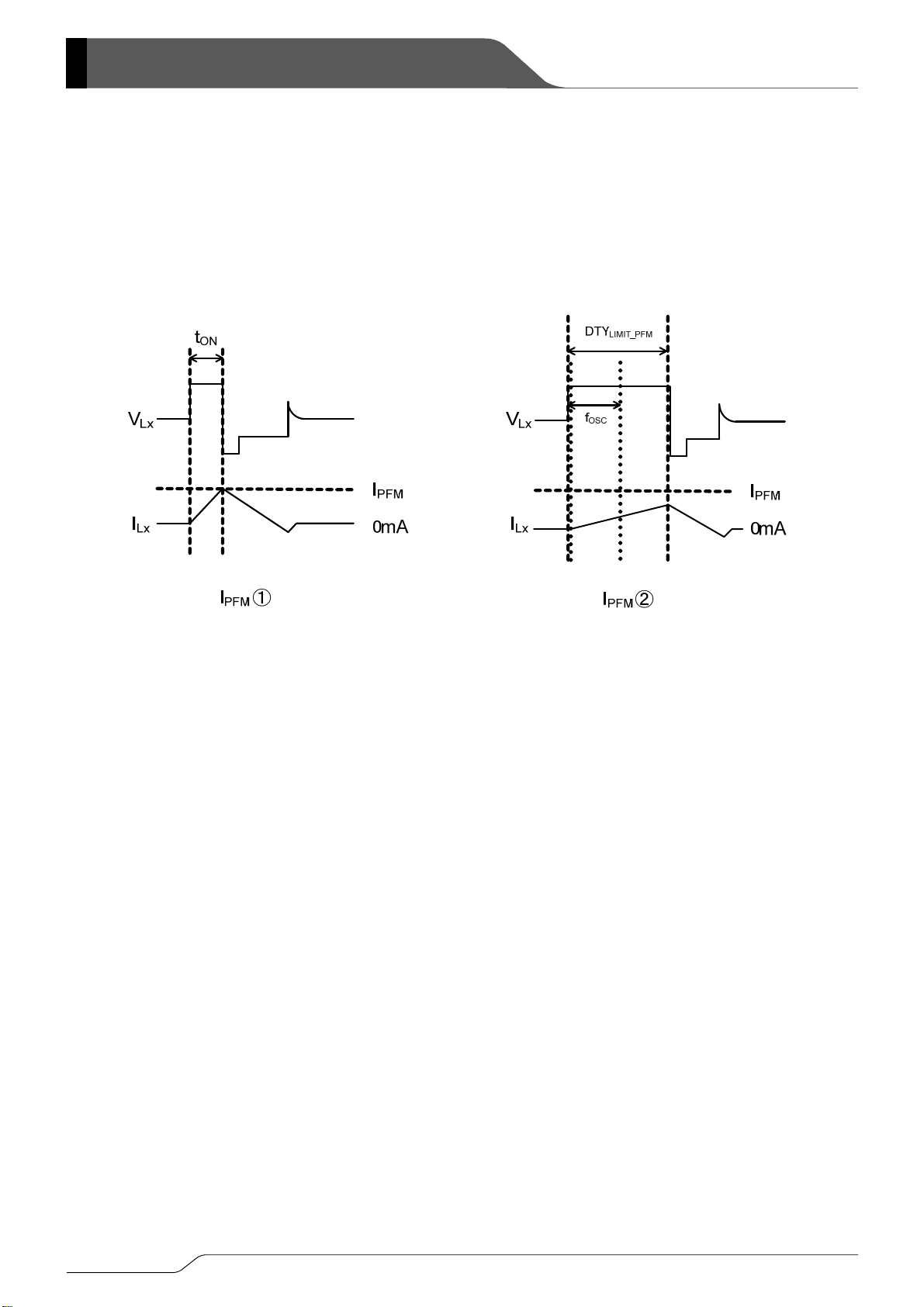
<PFM Switch Current>
(*1)
In PFM control operation, until coil current reaches to a specified level (IPFM), the IC keeps the P-channel MOS driver transistor on. In this
case, time that the P-channel MOS driver transistor is kept on (t
t
= L × I
ON
< PFM Duty Limit >
In PFM control operation, the PFM duty limit (DTY
PFM
/ (VIN - V
(*1)
OUT
)
LIMIT_PFM
) can be given by the following formula. Please refer to I
ON
PFM
①
) is set to 200% (TYP.). Therefore, under the condition that the duty increases (e.g.
the condition that the step-down ratio is small), it’s possible for P-channel MOS driver transistor to be turned off even when coil current doesn’t
reach to IPFM. Please refer to I
(*1)
XC9242 Series is excluded.
PFM
②
Fig. Fig.
10/27

XC9242/XC9243
Series
■NOTE ON USE
1. Please use this IC within the stated maximum ratings. For temporary, transitional voltage drop or voltage rising phenomenon,
the IC is liable to malfunction should the ratings be exceeded.
2. Where wiring impedance is high, operations may become unstable due to noise and/or phase lag depending on output current.
Please wire the input capacitor (C
3. When the difference between V
some cycles may be skipped completely.
4. When the difference between V
possibility that some cycles may be skipped completely.
5. With the IC, the peak current of the coil is controlled by the current limit circuit. Since the peak current increases when dropout voltage or
load current is high, current limit starts operation, and this can lead to instability. When peak current becomes high, please adjust the coil
inductance value and fully check the circuit operation. In addition, please calculate the peak current according to the following formula:
Ipk = (V
)×OnDuty / (2×L×f
IN-VOUT
L : Coil Inductance Value
f
: Oscillation Frequency
OSC
6. Use of the IC at voltages below the recommended voltage range may lead to instability.
7. This IC should be used within the stated absolute maximum ratings in order to prevent damage to the device.
8. When the IC is used in high temperature, output voltage may increase up to input voltage level at no load because of the leak current of the
P-channel driver transistor.
9. The XC9242/XC9243 uses fold-back circuit limiter. However, fold-back may become “droop” affected by the wiring conditions. Care
must be taken especially for C
10. If C
capacitance reduction happens such as in the case of low temperature, the IC may enter unstable operation. Care must be taken for
L
C
capacitor selection and its capacitance value.
L
) and the output capacitor (CL) as close to the IC as possible.
IN
and V
IN
and V
IN
distance and position.
IN
is large in PWM control, very narrow pulses will be outputted, and there is the possibility that
OUT
is small, and the load current is heavy, very wide pulses will be outputted and there is the
OUT
) + I
OUT
OSC
1ch VLx :2.0V/di
2ch V
:50mV/di
OUT
v
v
Ta = - 50
V
IN
C
IN
C
L
I
OUT
℃
= 3.6V, V
= 0.9V, f
OUT
= 20μF(Ceram ic)
= 14.7μF(Ceram ic)
= 300mA
= 2.4MHz
OSC
11. Torex places an importance on improving our products and its reliability.
However, by any possibility, we would request user fail-safe design and post-aging treatment on system or equipment.
11/27

r
f
XC9242/XC9243 Series
■NOTE ON USE (Continued)
●Instructions of pattern layouts
1. In order to stabilize VIN voltage level, we recommend that a by-pass capacitor (CIN) be connected as close as possible to the PVIN & PGND
pins and the AVIN & AGND pins.
2. Make sure to avoid noise from the PVIN pin to the AVIN pin. Please connect the AGND pin and PGND pin in the shortest length for wiring.
3. Please mount each external component as close to the IC as possible.
4. Wire external components as close to the IC as possible and use thick, short connecting traces to reduce the circuit impedance.
5. This series’ internal driver transistors bring on heat because of the output current and ON resistance of P-channel and N-channel MOS drive
transistors.
6. Make sure that the PCB GND traces are as thick as possible, as variations in ground potential caused by high ground currents at the time o
switching may result in instability of the IC.
●Recommended Pattern Layout(USP-10B)
st
Layer 2nd Layer
1
3rd Layer 4th Layer
●PCB (USP-10B) ●Typical Application Circuit (USP-10B)
1) XC9242/XC9243 Series 1) XC9242/XC9243 Series
USP-1 0B
12/27
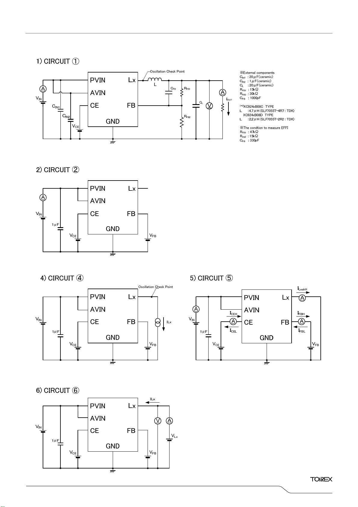
■TEST CIRCUITS
XC9242/XC9243
Series
13/27

XC9242/XC9243 Series
■TYPICAL PERFORMANCE CHARACTERISTICS
(1) Efficiency vs. Output Current
XC9242B08C (V
L=4.7μH(SLF7055),CIN=20μF(LMK212ABJ106KGx2)
=1μF(LMK107BJ105KAx1),CL=20μF(LMK212ABJ106KGx2)
C
IN
100
90
VIN=3.7V
80
70
60
50
40
30
Efficiency: EFFI (%)
20
10
0
0.1 1 10 100 1000 10000
Output Current: I
OUT
OUT
=1.2V)
R
=15kΩ, R
FB1
VIN=5.0V
(mA)
=30kΩ, CFB=1000pF
FB2
100
90
80
70
60
50
40
30
Efficiency: EFFI (%)
20
10
0
0.1 1 10 100 1000 10000
XC9243B08C (V
L=4.7μH(SLF7055),CIN=20μF(LMK212ABJ106KGx2)
=1μF(LMK107BJ105KAx1),CL=20μF(LMK212ABJ106KGx2)
C
IN
OUT
=1.2V)
=15kΩ, R
R
FB1
FB2
VIN=5.0V
VIN=3.7V
Output Current: I
OUT
(mA)
=30kΩ, CFB=1000pF
XC9242B08D (V
L=2.2μH(SLF7055),CIN=20μF(LMK212ABJ106KGx2)
C
=1μF(LMK107BJ105KAx1),CL=20μF(LMK212ABJ106KGx2)
IN
OUT
=1.2V)
100
90
80
VIN=3.7V
70
60
50
40
30
Efficiency: EFFI (%)
20
10
0
0.1 1 10 100 1000 10000
Output Current: I
OUT
(mA)
(2) Output Voltage vs. Output Current
1.4
XC9242B08C (V
L=4.7μH(SLF7055),CIN=20μF(LMK212ABJ106K Gx2)
C
=1μF(LMK107BJ105KAx1), CL=20μF(LMK212ABJ106K Gx2)
IN
OUT
=1.2V)
=
VIN=5.0V
=15kΩ, R
R
FB1
=
=30kΩ, CFB=1000pF
FB2
XC9243B08D (V
L=2.2μH(SLF7055),CIN=20μF(LMK212ABJ106KGx2)
=1μF(LMK107BJ105KAx1),CL=20μF(LMK212ABJ106KGx2)
C
=
IN
OUT
=1.2V)
=
=
=
100
90
80
70
60
VIN=5.0V
50
40
30
Efficiency: EFFI (%)
20
VIN=3.7V
10
0
0.1 1 10 100 1000 10000
Output Current: I
XC9243B08C (V
L=4.7μH(SLF7055),CIN=20μF(LMK212ABJ106K Gx2)
=1μF(LMK107BJ105KAx1),CL=20μF(LMK212ABJ106K Gx2)
C
IN
OUT
OUT
(mA)
=1.2V)
=
=
=
1.4
(V)
OUT
Output Voltage: V
14/27
1.3
1.2
VIN=3.7V, 5.0V
1.1
1
0.1 1 10 100 1000 10000
Output Current: I
OUT
(mA)
(V)
1.3
OUT
1.2
VIN=3.7V, 5.0V
1.1
Output Voltage: V
1
0.1 1 10 100 1000 10000
Output Current: I
OUT
(mA)

■TYPICAL PERFORMANCE CHARACTERISTICS (Continued)
(2) Output Voltage vs. Output Current
XC9242/XC9243
Series
XC9242B08D (V
L=2.2μH(SLF7055),C IN=20μF(LMK212ABJ106K Gx2)
CIN=1μF(LMK107BJ105KAx1),CL=20μF(LMK212ABJ106KGx2)
=1.2V)
OUT
RFB1=15kΩ, RFB2=30kΩ, CFB=1000pF
1.4
(V)
1.3
OUT
1.2
VIN=3.7V, 5.0V
1.1
Output Voltage: V
1
0.1 1 10 100 1000 10000
Output Current: I
OUT
(mA)
(3) Ripple Voltage vs. Output Current
XC9242B08C (V
L=4.7μH(SLF7055),CIN=20μF(LMK212ABJ106K Gx2)
C
=1μF(LMK107BJ105KAx1), CL=20μF(LMK212ABJ106K Gx2)
IN
100
90
80
70
60
50
40
30
Ripple Voltage: Vr(mV)
20
10
0
0.1 1 10 100 1000 10000
Output Current: I
V
= 3.7V
IN
OUT
OUT
=1.2V)
(mA)
R
FB1
=15kΩ, R
V
= 5.0V
IN
=30kΩ, CFB=1000pF
FB2
XC9243B08D (V
L=2.2μH(SLF7055),CIN=20μF(LMK212ABJ106K Gx2)
=1μF(LMK107BJ105KAx1),CL=20μF(LMK212ABJ106K Gx2)
C
IN
OUT
=1.2V)
R
FB1
=15kΩ, R
1.4
(V)
1.3
OUT
1.2
VIN=3.7V, 5.0V
1.1
Output Voltage: V
1
0.1 1 10 100 1000 10000
Output Current: I
XC9243B08C (V
L=4.7μH(SLF7055),CIN=20μF(LMK212ABJ106K Gx2)
C
=1μF(LMK107BJ105KAx1),CL=20μF(LMK212ABJ106K Gx2)
IN
OUT
OUT
(mA)
=1.2V)
R
=15kΩ, R
100
90
80
70
60
50
V
= 3.7V
40
IN
V
IN
= 5.0V
30
Ripple Voltage: Vr(mV)
20
10
0
0.1 1 10 100 1000 10000
Output Current: I
OUT
(mA)
=30kΩ, CFB=1000pF
FB2
=30kΩ, C
=1000pF
XC9242B08D (V
L=2.2μH(SLF7055),CIN=20μF(LMK212ABJ106K Gx2)
=1μF(LMK107BJ105KAx1), CL=20μF(LMK212ABJ106K Gx2)
C
IN
OUT
=1.2V)
R
FB1
=15kΩ, R
100
90
80
70
60
50
40
30
Ripple Voltage: Vr(mV)
20
V
= 5.0V, 3.7V
IN
10
0
0.1 1 10 100 1000 10000
Output Current: I
OUT
(mA)
=30kΩ, CFB=1000pF
FB2
XC9243B08D (V
L=2.2μH(SLF7055),CIN=20μF(LMK212ABJ106K Gx2)
=1μF(LMK107BJ105KAx1),CL=20μF(LMK212ABJ106K Gx2)
C
IN
OUT
=1.2V)
R
FB1
=15kΩ, R
=30kΩ, CFB=1000pF
FB2
100
90
80
V
= 3.7V
IN
70
V
= 5.0V
IN
60
50
40
30
Ripple Voltage: Vr(mV)
20
10
0
0.1 1 10 100 1000 10000
Output Current: I
OUT
(mA)
15/27

XC9242/XC9243 Series
■TYPICAL PERFORMANCE CHARACTERISTICS (Continued)
(4) FB Voltage vs. Ambient Temperature (5) UVLO Voltage vs. Ambient Temperature
XC9242B08C
0.88
0.86
(V)
0.84
FB
0.82
0.80
0.78
0.76
Feedback Voltage: V
0.74
0.72
-50 -25 0 25 50 75 100
Ambient Temperature: Ta (℃)
VIN = 6.0V
VIN = 5.0V
VIN = 4.0V
(6) Quiescent Current vs. Ambient Temperature
XC9242B08C
100
90
80
70
60
50
40
30
20
Quiescent Current: Iq (μA)
10
0
-50 -25 0 25 50 75 100
VIN = 6.0V
VIN = 5.0V
VIN = 4.0V
Ambient Temperature: Ta (℃)
XC9242B08C
2.7
2.6
2.5
2.4
2.3
2.2
UVLO Voltage: UVLO (V)
2.1
2.0
-50 -25 0 25 50 75 100
Ambient Temperature: Ta (℃)
UVLO
XC9242B08D
100
90
80
70
60
50
40
30
20
Quiescent Current: Iq (μA)
10
0
-50 -25 0 25 50 75 100
VIN = 6.0V
VIN = 5.0V
VIN = 4.0V
Ambient Temperature: Ta (℃)
(7) Stand-by Current vs. Ambient Temperature
XC9242B08C
5.0
VIN = 6.0V
4.0
(μA)
STB
3.0
2.0
1.0
Standby Current: I
0.0
-50 -25 0 25 50 75 100
Ambient Temperature: Ta (℃)
VIN = 5.0V
VIN = 4.0V
16/27
XC9242B08D
5.0
4.0
(μA)
STB
3.0
2.0
1.0
Standby Current: I
0.0
-50 -25 0 25 50 75 100
Ambient Temperature: Ta (℃)
VIN = 6.0V
VIN = 5.0V
VIN = 4.0V

■TYPICAL PERFORMANCE CHARACTERISTICS (Continued)
(8) Oscillation Frequency vs. Ambient Temperature
XC9242/XC9243
Series
XC9242B08C
1800
1600
(MHz)
OSC
1400
1200
1000
800
Oscillation Freqency: f
600
-50 -25 0 25 50 75 100
Ambient Temperature: Ta (℃)
VIN = 6.0V
VIN = 5.0V
VIN = 4.0V
(9) PFM Switching Current vs. Ambient Temperature
XC9243B08C
1000
900
800
(mA)
700
PFM
600
500
400
300
200
PFM SW Current: I
100
0
-50 -25 0 25 50 75 100
Ambient Temperature: Ta (℃)
VIN = 6.0V
VIN = 5.0V
VIN = 4.0V
XC9242B08D
3000
2800
(MHz)
OSC
2600
2400
2200
2000
Oscillation Freqency: f
1800
-50 -25 0 25 50 75 100
Ambient Temperature: Ta (℃)
VIN = 6.0V
VIN = 5.0V
VIN = 4.0V
XC9243B08D
2000
1800
1600
(mA)
1400
PFM
1200
1000
800
600
400
PFM SW Current: I
200
0
-50 -25 0 25 50 75 100
Ambient Temperature: Ta (℃)
VIN = 6.0V
VIN = 5.0V
VIN = 4.0V
(10) PFM Duty Limit vs. Ambient Temperature
XC9243B08C
300
(%)
250
LIMIT_PFM
200
150
100
50
PFM Duty Limit: DTY
0
-50 -25 0 25 50 75 100
Ambient Temperature: Ta (℃)
XC9243B08D
300
(%)
250
LIMIT_PFM
200
150
100
50
PFM Duty Limit: DTY
0
-50 -25 0 25 50 75 100
Ambient Temperature: Ta (℃)
17/27

XC9242/XC9243 Series
■TYPICAL PERFORMANCE CHARACTERISTICS (Continued)
(11) Pch Driver ON Resistance vs. Ambient Temperature (12) Nch Driver ON Resistance vs. Ambient Temperature
XC9242B08C
300
(mΩ)
250
LxH
200
150
100
50
0
Lx SW Pch ON Resistance: R
-50 -25 0 25 50 75 100
Ambient Temperature: Ta (℃)
VIN = 6.0V
VIN = 5.0V
VIN = 4.0V
300
(mΩ)
250
LxL
200
150
100
50
0
Lx SW Nch ON Resistance: R
-50 -25 0 25 50 75 100
XC9242B08C
VIN = 6.0V
VIN = 5.0V
VIN = 4.0V
Ambient Temperature: Ta (℃)
(13) LxSW”H” Leakage Current vs. Ambient Temperature (14) Current Limit vs. Ambient Temperature
XC9242B08C
5.0
(μA)
Lx
4.0
3.0
VIN = 6.0V
VIN = 5.0V
VIN = 4.0V
8000
7000
(mA)
6000
LIM
5000
XC9242B08C
VIN = 6.0V
VIN = 5.0V
VIN = 4.0V
2.0
4000
1.0
0.0
LxSW”H” Leakage Current: I
-50 -25 0 25 50 75 100
Ambient Temperature : Ta (℃)
Current Limit: I
3000
2000
-50 -25 0 25 50 75 100
Ambient Temperature : Ta (℃)
(15) CE”H” Voltage vs. Ambient Temperature (16) CE”L” Voltage vs. Ambient Temperature
XC9242B08C
1.4
1.2
(V)
1.0
CEH
0.8
0.6
0.4
CE”H” Voltage V
0.2
0.0
-50 -25 0 25 50 75 100
Ambient Temperature: Ta (℃)
VIN = 6.0V
VIN = 5.0V
VIN = 4.0V
1.4
1.2
(V)
1.0
CEL
0.8
0.6
0.4
CE”L” Voltage V
0.2
0.0
-50 -25 0 25 50 75 100
XC9242B08C
Ambient Temperature: Ta (℃)
18/27
VIN = 6.0V
VIN = 5.0V
VIN = 4.0V

■TYPICAL PERFORMANCE CHARACTERISTICS (Continued)
(18) C
(17) Soft-Start Time vs. Ambient Temperature
Discharge Resistance vs. Ambient Temperature
L
XC9242/XC9243
Series
XC9242B08C
2.0
1.8
1.6
(ms)
SS
1.4
VIN = 6.0V
VIN = 5.0V
VIN = 4.0V
1.2
1.0
0.8
0.6
0.4
Soft-Start Time: t
0.2
0.0
-50 -25 0 25 50 75 100
Ambient Temperature: Ta (℃)
XC9242B08C
300
(Ω)
250
DCHG
200
150
100
50
Discharge Resistance: R
L
C
0
-50 -25 0 25 50 75 100
Ambient Temperature: Ta (℃)
VIN = 6.0V
VIN = 5.0V
VIN = 4.0V
19/27

XC9242/XC9243 Series
■TYPICAL PERFORMANCE CHARACTERISTICS (Continued)
(19) Load Transient Response
XC9242B08C
VIN = 5.0V, V
= 1.2V, I
OUT
= 1mA ⇒ 1.5
OUT
A
V
: 100mV/div
OUT
ILx : 1.0A/div
VIN = 5.0V, V
L=4.7μH(SLF7055),C
C
=1μF(LMK107BJ105KAx1),CL=20μF(LMK212ABJ106KGx2)
IN2
= 1.2V, I
OUT
OUT
V
: 200mV/div
OUT
ILx : 1.0A/div
IN1
R
=15kΩ, R
FB1
= 1.5A ⇒ 1m
=20μF(LMK212ABJ106KGx2)
=30kΩ, CFB=1000pF
FB2
A
VIN = 5.0V, V
20/27
= 1.2V, I
OUT
= 1mA ⇒ 1.5
OUT
A
V
: 100mV/div
OUT
ILx : 1.0A/div
XC9243B08C
VIN = 5.0V, V
L=4.7μH(SLF7055),C
C
=1μF(LMK107BJ105KAx1),CL=20μF(LMK212ABJ106KGx2)
IN2
= 1.2V, I
OUT
V
OUT
: 200mV/div
OUT
= 1.5A ⇒ 1m
ILx : 1.0A/div
=20μF(LMK212ABJ106KGx2)
IN1
R
=15kΩ, R
FB1
=30kΩ, CFB=1000pF
FB2
A

■TYPICAL PERFORMANCE CHARACTERISTICS (Continued)
(19) Load Transient Response
XC9242B08D
VIN = 5.0V, V
OUT
= 1.2V, I
= 1mA ⇒ 1.5A VIN = 5.0V, V
OUT
V
: 100mV/div
OUT
ILx : 1.0A/div
L=2.2μH(SLF7055),C
C
=1μF(LMK107BJ105KAx1),CL=20μF(LMK212ABJ106KGx2)
IN2
= 1.2V, I
OUT
= 1.5A ⇒ 1mA
OUT
V
: 200mV/div
OUT
ILx : 1.0A/div
R
FB1
IN1
=15kΩ, R
XC9242/XC9243
=20μF(LMK212ABJ106KGx2)
=30kΩ, CFB=1000pF
FB2
Series
VIN = 5.0V, V
= 1.2V, I
OUT
= 1mA ⇒ 1.5
OUT
A
V
: 100mV/div
OUT
ILx : 1.0A/div
XC9243B08D
VIN = 5.0V, V
L=2.2μH(SLF7055),C
C
=1μF(LMK107BJ105KAx1),CL=20μF(LMK212ABJ106KGx2)
IN2
= 1.2V, I
OUT
V
: 200mV/div
OUT
= 1.5A ⇒ 1m
OUT
ILx : 1.0A/div
=20μF(LMK212ABJ106KGx2)
IN1
R
=15kΩ, R
FB1
=30kΩ, CFB=1000pF
FB2
A
21/27

XC9242/XC9243 Series
■TYPICAL PERFORMANCE CHARACTERISTICS (Continued)
(20) Frequency Response
Test Condition:
Measurement equipment:NF FRA5097 Version:3.00
OSC amplitude=20.0mVpeak OSC.Dcbias=0.00V
OSC waveform:SIN, Sweep minimum frequency=1Hz
Sweep maximum frequency=15MHz
Sweep resolution=300steps/sweep
Integration period=100cycle, Delay time=0cycle
Order of harmonic analysis=1, Measure mode:CH1&CH2
Auto integration:OFF, Amplitude compression:OFF
Slow sweep:OFF
XC9242B08CDR
L=4.7μH(SLF7055), CIN=20μF(LMK212ABJ106KGx2)
=1μF(LMK107BJ105KAx1),CL=20μF(LMK212ABJ106KGx2)
C
IN
=15kΩ, R
R
FB1
=5.0V, VCE=VIN, V
V
IN
L=4.7μH(SLF7055),C
=1μF(LMK107BJ105KAx1),CL=20μF(LMK212ABJ106KGx2)
C
IN
=15kΩ, R
R
FB1
=5.0V, VCE=VIN, V
V
IN
22/27
=30kΩ, CFB=1000pF
FB2
=1.2V, I
OUT
=20μF(LMK212ABJ106KGx2)
IN
=30kΩ, CFB=1000pF
FB2
=1.2V, I
OUT
=1mA
OUT
=1000mA
OUT

■TYPICAL PERFORMANCE CHARACTERISTICS (Continued)
(20) Frequency Response (Continued)
Test Condition:
Measurement equipment:NF FRA5097 Version:3.00
OSC amplitude=20.0mVpeak OSC.Dcbias=0.00V
OSC waveform:SIN, Sweep minimum frequency=1Hz
Sweep maximum frequency=15MHz
Sweep resolution=300steps/sweep
Integration period=100cycle, Delay time=0cycle
Order of harmonic analysis=1, Measure mode:CH1&CH2
Auto integration:OFF, Amplitude compression:OFF
Slow sweep:OFF
XC9242B08DDR
L=2.2μH(SLF7055),CIN=20μF(LMK212ABJ106KGx2)
=1μF(LMK107BJ105KAx1),CL=20μF(LMK212ABJ106KGx2)
C
IN
=15kΩ, R
R
FB1
=5.0V, VCE=VIN, V
V
IN
L=2.2μH(SLF7055),C
=1μF(LMK107BJ105KAx1),CL=20μF(LMK212ABJ106KGx2)
C
IN
=15kΩ, R
R
FB1
=5.0V, VCE=VIN, V
V
IN
=30kΩ, CFB=1000pF
FB2
=1.2V, I
OUT
IN
=30kΩ, CFB=1000pF
FB2
OUT
OUT
=20μF(LMK212ABJ106KGx2)
=1.2V, I
OUT
=1mA
=1000mA
XC9242/XC9243
Series
23/27

XC9242/XC9243 Series
■PACKAGING INFORMATION
●USP-10B
*The sides of a package are nickel, not plated with Au.
*No1,2,9,10 pins are thicker than other pins.
24/27

XC9242/XC9243
■ PACKAGING INFORMATION (Continued)
●USP-10B Reference Pattern Layout ●USP-10B Reference Metal Mask Design
1.45 1.45
0.35 1.10 1.10 0.35
0.70 0.70
0.0250.025
0.125
0.125
0.125
1.25
0.125
1.35
Series
0.25
0.025
0.4750.475
0.025
0.125
0.225
0.25
0.125
0.25
0.225
1.25
1.35
0.15 0.15
25/27

XC9242/XC9243 Series
■MARKING RULE
●USP-10B
1
2
3
4
5
⑤ ⑥④
② ③①
10
9
8
7
6
26/27
① represents product series
MARK PRODUCT SERIES
② represents product function
MARK FUNCTION PRODUCT SERIES
③ represents product function
MARK OUTPUT VOLTAGE (V) PRODUCT SERIES
④ represents product function
MARK OSCILLATION FREQUENCY (MHz) PRODUCT SERIES
⑤⑥ represents production lot number
01 to 09, 0A to 0Z 11 to 9Z, AA to AZ, B1 to ZZ repeated
(G, I, J, O, Q, W excluded)
*No character inversion used.
B XC9242******-G
C XC9243******-G
B CL High Speed Discharge XC9242B*****-G
8 0.8 XC9242B08***-G
C 1.2 XC9242B**C**-G
D 2.4 XC9242B**D**-G

XC9242/XC9243
Series
1. The products and product specifications contained herein are subject to change without
notice to improve performance characteristics. Consult us, or our representatives
before use, to confirm that the information in this datasheet is up to date.
2. We assume no responsibility for any infringement of patents, patent rights, or other
rights arising from the use of any information and circuitry in this datasheet.
3. Please ensure suitable shipping controls (including fail-safe designs and aging
protection) are in force for equipment employing products listed in this datasheet.
4. The products in this datasheet are not developed, designed, or approved for use with
such equipment whose failure of malfunction can be reasonably expected to directly
endanger the life of, or cause significant injury to, the user.
(e.g. Atomic energy; aerospace; transport; combustion and associated safety
equipment thereof.)
5. Please use the products listed in this datasheet within the specified ranges.
Should you wish to use the products under conditions exceeding the specifications,
please consult us or our representatives.
6. We assume no responsibility for damage or loss due to abnormal use.
7. All rights reserved. No part of this datasheet may be copied or reproduced without the
prior permission of TOREX SEMICONDUCTOR LTD.
27/27
 Loading...