

)
yp
y
p
A
XC9235/XC9236/XC9237
Series
ETR0514-012
600mA Driver Tr. Built-In, Synchronous Step-Down DC/DC Converters
■GENERAL DESCRIPTION
The XC9235/XC9236/XC9237 series is a group of synchronous-rectification type DC/DC converters with a built-in 0.42Ω
P-channel MOS driver transistor and 0.52ΩN-channel MOS switching transistor, designed to allow the use of ceramic
capacitors. Operating voltage range is from 2.0V to 6.0V (A~C types), 1.8V to 6.0V (D~G types). For the D/F types which
have a reference voltage of 0.8V (accuracy: ±2.0%), the output voltage can be set from 0.9V by using two external resistors.
The A/B/C/E/G types have a fixed output voltage from 0.8V to 4.0V in increments of 0.05V (accuracy: ±2.0%). The device
provides a high efficiency, stable power supply with an output current of 600mA to be configured using only a coil and two
capacitors connected externally. With the built-in oscillator, either 1.2MHz or 3.0MHz can be selected for suiting to your
particular application. As for operation mode, the XC9235 series is PWM control, the XC9236 series is automatic PWM/PFM
switching control and the XC9237 series can be manually switched between the PWM control mode and the automatic
PWM/PFM switching control mode, allowing fast response, low ripple and high efficiency over the full range of loads (from light
load to heavy load).
The soft start and current control functions are internally optimized. During stand-by, all circuits are shutdown to reduce current
consumption to as low as 1.0μA or less. The B/F/G types have a high speed soft-start as fast as 0.25ms in typical for quick
turn-on. With the built-in UVLO (Under Voltage Lock Out) function, the internal P-channel MOS driver transistor is forced OFF
when input voltage becomes 1.4V or lower.
The B to G types integrate C
via the internal discharge switch located between the L
quickly returns to the V
Three t
■APPLICATIONS
●Mobile phones, Smart phones
●Bluetooth headsets
●Mobile WiMAX PDAs, MIDs, UMPCs
●Portable game consoles
●Digital cameras, Camcorders
●MP3 Players, Portable Media Players
●Notebook computers
■
●XC9235/XC9236/XC9237
●XC9235/XC9236/XC9237
D/F types (Output Voltage Externally Set)
es of package SOT-25 (A/B/C types only), USP-6C, and 0.4mm low height USP-6EL (A/B/C types only) are available.
TYPICAL APPLICATION CIRCUIT
/B/C/E/G types (Output Voltage Fixed)
discharge function which enables the electric charge at the output capacitor CL to be discharged
L
level as a result of this function.
SS
and VSS pins. When the devices enter stand-by mode, output voltage
X
■FEATURES
Driver Transistor Built-In
Input Voltage : 2.0V ~ 6.0V (A/B/C types)
1.8V ~ 6.0V (D/E/F/G types)
Output Voltage : 0.8V ~ 4.0V (Internally set)
High Efficiency : 92% (TYP.)
Output Current : 600mA
Oscillation Frequency : 1.2MHz, 3.0MHz (+15%)
Maximum Duty Cycle : 100%
Control Methods : PWM (XC9235)
PWM/PFM Auto (XC9236)
Function
Capacitor
Operating Ambient Temperature
Packages : SOT-25 (A/B/C types only), USP-6C
USP-6EL(A/B/C types only)
Environmentally Friendl
■
TYPICAL PERFORMANCE CHARACTERISTICS
●Efficiency vs. Output Current(f
PWM/PFM Automatic Sw itching Control
100
90
80
VIN= 4.2V
70
3.6V
60
2.4V
50
40
30
Efficency:EFFI(%
Efficiency: EFFI (%)
20
10
0
0.1 1 10 100 1000
Output Current:IOUT(mA)
☆GreenOperation Compatible
: 0.42Ω P-ch driver transistor
0.52Ω N-ch switch transistor
0.9V ~ 6.0V (Externally set)
PWM/PFM Manual (XC9237)
: Current Limiter Circuit Built-In
(Constant Current & Latching)
C
Discharge (B/C/D/E/F/G types)
L
High Speed Soft Start (B/F/G type)
:
Low ESR Ceramic Capacitor
:-40℃ ~ +85℃
: EU RoHS Com
=1.2MHz, VOUT=1.8V)
OSC
PWM Control
VIN= 4.2V
3.6V
2.4V
liant, Pb Free
1/33

to other pins, it should be connected to the
XC9235/XC9236/XC9237
■PIN CONFIGURATION
Lx VOUT
5 4
VIN 6
VSS 5
CE/MODE 4
132
VSS CE/MODEVIN
SOT-25
(Top View)
Series
USP-6C
(BOTTOM VIEW)
* Please short the VSS pin (No. 2 and 5).
* The dissipation pad for the USP-6C package should be solder-plated
in recommended mount pattern and metal masking so as to enhance
mounting strength and heat release. If the pad needs to be connected
1 Lx
2 VSS
3 VOUT (FB)
VIN 6
VSS 5
CE/MODE 4
V(No. 5) pin.
1 Lx
2 VSS
3 VOUT
USP-6EL
(BOTTOM VIEW)
■PIN ASSIGNMENT
PIN NUMBER
SOT-25 USP-6C/USP-6EL
1 6 VIN Power Input
2 2, 5 VSS Ground
3 4 CE / MODE High Active Enable / Mode Selection Pin
4 3
5 1 Lx Switching Output
2/33
PIN NAME FUNCTION
VOUT
FB
Fixed Output Voltage Pin (A/B/C/E/G types)
Output Voltage Sense Pin (D/F types)

XC9235/XC9236/XC9237
■PRODUCT CLASSIFICATION
●Ordering Information
XC9235①②③④⑤⑥-⑦
XC9236①②③④⑤⑥-⑦
XC9237①②③④⑤⑥-⑦
DESIGNATOR ITEM SYMBOL DESCRIPTION
Fixed Output voltage (V
①
Functional selection
Adjustable Output voltage (FB)
Functional selection
Fixed Output Voltage
②③
Adjustable Output Voltage
④
Oscillation Frequency
⑤⑥-⑦
(*1)
The “-G” suffix indicates that the products are Halogen and Antimony free as well as being fully RoHS compliant.
(*2)
SOT-25, USP-6EL package are available for the A/B/C series only.
(*1)
Fixed PWM control
(*1)
PWM / PFM automatic switching control
(*1)
Fixed PWM control QPWM / PFM automatic switching manual selection
A VIN≧2.0V, No CL discharge, Low speed soft-start
B VIN≧2.0V, CL discharge, High speed soft-start
)
OUT
C VIN≧2.0V, CL discharge, Low speed soft-start
E VIN≧1.8V, CL discharge, Low speed soft-start
G V
≧1.8V, CL discharge, High speed soft-start
IN
D VIN≧1.8V, CL discharge, Low speed soft-start
F VIN≧1.8V, CL discharge, High speed soft-start
Output voltage options
(V
OUT
e.g. V
)
08 ~ 40
0.05V increments: 0.05=A, 0.15=B, 0.25=C, 0.35=D, 0.45=E,
=2.8V→②=2, ③=8
OUT
V
=2.85V→②=2, ③=L
OUT
0.55=F, 0.65=H, 0.75=K, 0.85=L, 0.95=M
Reference voltage is fixed in 0.8V
②=0, ③=8
(FB)
08
C 1.2MHz
D 3.0MHz
(*2)
(3,000/Reel)
(*2)
(3,000/Reel)
Packages
(Order Unit)
MR SOT-25
MR-G SOT-25
ER USP-6C (3,000/Reel)
ER-G USP-6C (3,000/Reel)
(*2)
4R-G USP-6EL
(3,000/Reel)
Series
3/33
XC9235/XC9236/XC9237
Series
■BLOCK DIAGRAM
●XC9235 / XC9236 / XC9237
A Series
●XC9235 / XC9236 / XC9237
D/F Series
■ABSOLUTE MAXIMUM RATINGS
Power Dissipation
NOTE: The signal from CE/MODE Control Logic to PWM/PFM Selector is being fixed to "L" level inside,
and XC9235 series chooses only PWM control.
The signal from CE/MODE Control Logic to PWM/PFM Selector is being fixed to "H" level inside,
and XC9236 series chooses only PWM/PFM automatic switching control.
Diodes inside the circuit are ESD protection diodes and parasitic diodes.
PAR AMETER SYMBOL RATINGS UNIT
VIN Pin Voltage VIN - 0.3 ~ 6.5 V
Lx Pin Voltage VLx - 0.3 ~ VIN + 0.3 V
V
Pin Voltage V
OUT
FB Pin Voltage VFB - 0.3 ~ 6.5 V
CE / MODE Pin Voltage VCE - 0.3 ~ 6.5 V
Lx Pin Current ILx ±1500 mA
SOT-25 250
(*Ta=25℃)
Operating Ambient Temperature Topr - 40 ~ + 85
Storage Temperature Tstg - 55 ~ + 125
USP-6C 120
USP-6EL
- 0.3 ~ 6.5 V
OUT
Pd
●XC9235 / XC9236 / XC9237
B/C/E/G Series
120
Ta =2 5℃
mW
O
C
O
C
4/33

■ELECTRICAL CHARACTERISTICS
XC9237A18Cxx, V
OUT
=1.8V, f
=1.2MHz, Ta=25℃
OSC
XC9235/XC9236/XC9237
Series
PARAMETER SYMBOL CONDITIONS MIN. TYP. MAX. UNIT
Output Voltage V
OUT
When connected to external components,
V
IN=VCE
=5.0V, I
=30mA
OUT
1.764 1.800 1.836 V ①
Operating Voltage Range VIN 2.0 - 6.0 V ①
V
Maximum Output Current I
UVLO Voltage V
OUTMAX
UVLO
Supply Current IDD V
Stand-by Current I
Oscillation Frequency f
PFM Switching Current I
PFM Duty Limit DTY
Maximum Duty Cycle DTY
Minimum Duty Cycle DTY
Efficiency
(*2)
EFFI
Lx SW "H" ON Resistance 1 R
Lx SW "H" ON Resistance 2 R
Lx SW "L" ON Resistance 1 R
Lx SW "L" ON Resistance 2 R
Lx SW "H" Leak Current
Lx SW "L" Leak Current
Current Limit
(*5)
I
(*5)
I
(*10)
I
Output Voltage
Temperature Characteristics
(V
CE "H" Voltage V
CE "L" Voltage V
VIN=5.0V, VCE=0V, V
STB
OSC
PFM
LIMIT_PFM
MAX
MIN
LxH
LxH
VIN=VCE=5.0V
LxL
VIN=VCE=3.6V
LxL
LeakH
LeakL
V
LIM
△V
OUT
・△Topr)
OUT
CEH
CEL
IN=VOUT(E)
When connected to external components
V
CE
Voltage which Lx pin holding “L” level
IN=VCE
When connected to external components,
V
IN=VOUT(E)
When connected to external components,
V
IN=VOUT(E)
VCE=VIN=(C-1), I
VIN=VCE=5.0V, V
VIN=VCE=5.0V, V
When connected to external components,
V
CE=VIN=VOUT(E)
VIN=VCE=5.0V, V
VIN=VCE=3.6V, V
VIN=V
VIN=V
IN=VCE
/
I
OUT
V
OUT
Voltage changes Lx to “H” level
V
OUT
Voltage changes Lx to “L” level
When connected to external components,
PWM "H" Level Voltage V
PWMH
I
OUT
becomes 1020 kHz≦f
When connected to external components,
PWM "L" Level Voltage V
PWML
I
OUT
becomes f
CE "H" Current I
CE "L" Current I
Soft Start Time tSS
Latch Time t
Short Protection Threshold
Voltage
Test conditions: Unless otherwise stated, VIN=5.0V, V
NOTE:
*1: Including hysteresis operating voltage range.
*2: EFFI = { ( output voltage×output current ) / ( input voltage×input current) }×100
*3: ON resistance (Ω)= (V
*4: R&D value
*5: When temperature is high, a current of approximately 10μA (maximum) may leak.
*6: The CE/MODE pin of the XC9237A series works also as an external switching pin of PWM control and PWM/PFM control. When the IC is in the operation,
control is switched to the automatic PWM/PFM switching mode when the CE/MODE pin voltage is equal to or greater than V
mode when the CE/MODE pin voltage is equal to or lower than V
*7: Time until it short-circuits V
*8: When V
*9: When the difference between the input and the output is small, some cycles may be skipped completely before current maximizes.
*10: Current limit denotes the level of detection at peak of coil current.
*11: “H”=V
*12: XC9235 series exclude I
*13: XC9235/9236 series exclude V
is less than 2.4V, limit current may not be reached because voltage falls caused by ON resistance.
IN
If current is further pulled from this state, output voltage will decrease because of P-ch driver ON resistance.
-1.2V, “L”=+0.1V~-0.1V
IN~VIN
- Lx pin measurement voltage) / 100mA
IN
PFM
VIN=VCE=5.0V, V
CEH
VIN=5.0V, VCE=0V, V
CEL
When connected to external components,
V
CE
V
LAT
IN=VCE
Short Lx at 1Ω resistance
Sweeping V
V
SHORT
1Ω resistance, V
“L” level within 1ms
OUT(E)
with GND via 1Ωof resistor from an operational state and is set to Lx=0V from current limit pulse generating.
OUT
and DTY
PWMH
because those are only for the PFM control’s functions.
LIMIT_PFM
and V
because those are only for the XC9237 series’ functions.
PWML
+2.0V, VCE=1.0V,
=VIN, V
OUT
OUT
=0V,
OUT
=5.0V, V
OUT=VOUT(E)
+2.0V, VCE =1.0V, I
+2.0V, VCE =VIN, I
OUT
OUT=VOUT(E)
OUT=VOUT(E)
+1.2V, I
OUT
OUT
(*4)
- 0.45 0.65 Ω ④
(*4)
×1.1V - 15 33 μA ②
OUT=VOUT(E)
=1mA
×1.1V - 0 1.0 μA ②
=100mA
OUT
=1mA
OUT
(*12)
200 300 % ①
×0.9V 100 - - % ③
×1.1V - - 0 % ③
=100mA
OUT
=0V, ILx=100mA
=0V, ILx=100mA
=5.0V, VCE=0V, Lx=0V - 0.01 1.0 μA ⑤
=5.0V, VCE=0V, Lx=5.0V - 0.01 1.0 μA ⑤
=5.0V, V
OUT=VOUT(E)
×0.9V
(*9)
(*1, *11)
(*12)
(*3)
- 0.35 0.55 Ω ④
(*3)
- 0.42 0.67 Ω ④
(*8)
900 1050 1350 mA ⑥
=30mA, -40℃≦Topr≦85℃ - ±100 -
=0V, Applied voltage to VCE,
=0V, Applied voltage to VCE ,
(*6)
=1mA
=1mA
=0V → VIN, I
, Voltage which oscillation frequency
OSC
(*6)
, Voltage which oscillation frequency
<1020kHz
OSC
=0V - 0.1 - 0.1 μA ⑤
OUT
=0V - 0.1 - 0.1 μA ⑤
OUT
=1mA
=5.0V, V
OUT
=0.8×V
OUT
, VIN=VCE=5.0V, Short Lx at
OUT
voltage which Lx becomes
OUT
(*11)
(*11)
≦1380kHz
(*13)
,
OUT(E)
(*7)
(*13)
600 - - mA ①
1.00 1.40 1.78 V ③
1020 1200 1380 kHz ①
120 160 200 mA ①
- 92 - % ①
- 0.52 0.77 Ω -
ppm/
0.65 - 6.0 V ③
V
- 0.25 V ③
SS
- - V
–
V
IN
0.25
- 1.0 V ①
IN
- - V ①
0.5 1.0 2.5 ms ①
1.0 - 20.0 ms ⑦
0.675 0.900 1.150 V ⑦
=Nominal Voltage
minus 0.3V, and to the PWM
minus 1.0V and equal to or greater than V
IN
CEH
.
IN
℃
CIRCUIT
①
5/33
XC9235/XC9236/XC9237
Series
■ELECTRICAL CHARACTERISTICS (Continued)
XC9237A18Dxx, V
OUT
=1.8V, f
=3.0MHz, Ta=25℃
OSC
PARAMETER SYMBOL CONDITIONS MIN. TYP. MAX. UNIT
Output Voltage V
OUT
When connected to external components,
V
IN=VCE
=5.0V, I
OUT
=30mA
1.764 1.800 1.836 V ①
Operating Voltage Range VIN 2.0 - 6.0 V ①
Maximum Output Current I
UVLO Voltage V
OUTMAX
UVLO
V
When connected to external components
V
Voltage which Lx pin holding “L” level
Supply Current IDD VIN=VCE=5.0V, V
Stand-by Current I
Oscillation Frequency f
PFM Switching Current I
PFM Duty Limit DTY
Maximum Duty Cycle DTY
Minimum Duty Cycle DTY
Efficiency EFFI
Lx SW "H" ON Resistance 1 R
Lx SW "H" ON Resistance 2 R
Lx SW "L" ON Resistance 1 R
Lx SW "L" ON Resistance 2 R
Lx SW "H" Leak Current
Lx SW "L" Leak Current
Current Limit
(*5)
I
(*5)
I
(*10)
I
Output Voltage
Temperature Characteristics
(V
CE "H" Voltage V
CE "L" Voltage V
VIN=5.0V, VCE=0V, V
STB
When connected to external components,
OSC
PFM
LIMIT_PFM
V
When connected to external components,
V
VCE=VIN=(C-1), I
VIN=VCE=5.0V, V
MAX
VIN=VCE=5.0V, V
MIN
When connected to external components,
V
VIN=VCE=5.0V, V
LxH
VIN=VCE=3.6V, V
LxH
VIN=VCE=5.0V
LxL
VIN=VCE=3.6V
LxL
VIN=V
LeakH
VIN=V
LeakL
VIN=VCE=5.0V, V
LIM
△V
/
・△Topr)
OUT
CEH
CEL
OUT
I
V
Voltage changes Lx to “H” level
V
Voltage changes Lx to “L” level
When connected to external components,
PWM "H" Level Voltage V
PWMH
I
becomes 2550kHz≦f
When connected to external components,
PWM "L" Level Voltage V
PWML
I
becomes f
CE "H" Current I
CE "L" Current I
Soft Start Time tSS
Latch Time t
Short Protection Threshold
Voltage
VIN=VCE=5.0V, V
CEH
VIN=5.0V, VCE=0V, V
CEL
When connected to external components,
V
LAT
Short Lx at 1Ω resistance
V
Sweeping V
V
SHORT
1Ω resistance, V
“L” level within 1ms
IN=VOUT(E)
CE=VIN
IN=VOUT(E)
IN=VOUT(E)
CE=VIN=VOUT(E)
OUT
OUT
OUT
OUT
OUT
CE
IN=VCE
+2.0V, VCE=1.0V,
, V
=0V,
OUT
OUT=VOUT(E)
+2.0V, VCE=1.0V, I
+2.0V, VCE=VIN, I
OUT
OUT=VOUT(E)
OUT=VOUT(E)
+1.2V, I
OUT
OUT
(*4)
(*4)
=5.0V, VCE=0V, Lx=0V - 0.01 1.0 μA ⑤
OUT
=5.0V, VCE=0V, Lx=5.0V - 0.01 1.0 μA ⑤
OUT
OUT=VOUT(E)
×1.1V - 21 35 μA ②
OUT=VOUT(E)
=1mA
×1.1V - 0 1.0 μA ②
=100mA
OUT
=1mA
OUT
(*12)
- 200 300 % ①
×0.9V 100 - - % ③
×0.1V - - 0 % ③
=100mA
OUT
=0V, ILx=100mA
=0V, ILx=100mA
×0.9V
(*9)
(*1,*11)
(*12)
(*3)
- 0.35 0.55 Ω ④
(*3)
(*8)
900 1050 1350 mA ⑥
=30mA, -40℃≦Topr≦85℃ - ±100 -
=0V, Applied voltage to VCE,
=0V, Applied voltage to VCE,
(*6)
=1mA
=1mA
=0V → VIN, I
, Voltage which oscillation frequency
OSC
(*6)
, Voltage which oscillation frequency
<2550kHz
OSC
=0V - 0.1 - 0.1 μA ⑤
OUT
=0V - 0.1 - 0.1 μA ⑤
OUT
=1mA
=5.0V, V
OUT
=0.8×V
OUT
, VIN=VCE=5.0V, Short Lx at
OUT
voltage which Lx becomes
OUT
(*11)
(*11)
≦3450kHz
(*13)
,
OUT(E)
(*7)
(*13)
600 - - mA ①
1.00 1.40 1.78 V ③
2550 3000 3450 kHz ①
170 220 270 mA ①
- 86 - % ①
- 0.42 0.67 Ω ④
- 0.45 0.65 Ω -
- 0.52 0.77 Ω -
ppm/
0.65 - 6.0 V ③
V
- 0.25 V ③
SS
- - V
V
–
IN
0.25
- 1.0 V ①
IN
- - V ①
0.5 0.9 2.5 ms ①
1.0 - 20 ms ⑦
0.675 0.900 1.150 V ⑦
Test conditions: Unless otherwise stated, VIN=5.0V, V
NOTE:
*1: Including hysteresis operating voltage range.
*2: EFFI = { ( output voltage×output current ) / ( input voltage×input current) }×100
*3: ON resistance (Ω)= (V
*4: R&D value
*5: When temperature is high, a current of approximately 10μA (maximum) may leak.
*6: The CE/MODE pin of the XC9237A series works also as an external switching pin of PWM control and PWM/PFM control. When the IC is in the operation,
control is switched to the automatic PWM/PFM switching mode when the CE/MODE pin voltage is equal to or greater than V
mode when the CE/MODE pin voltage is equal to or lower than V
*7: Time until it short-circuits V
*8: When V
*9: When the difference between the input and the output is small, some cycles may be skipped completely before current maximizes.
*10: Current limit denotes the level of detection at peak of coil current.
*11: “H”=V
*12: XC9235 series exclude I
*13: XC9235/9236 series exclude V
is less than 2.4V, limit current may not be reached because voltage falls caused by ON resistance.
IN
If current is further pulled from this state, output voltage will decrease because of P-ch driver ON resistance.
-1.2V, “L”=+0.1V~-0.1V
IN~VIN
- Lx pin measurement voltage) / 100mA
IN
with GND via 1Ωof resistor from an operational state and is set to Lx=0V from current limit pulse generating.
OUT
and DTY
PFM
LIMIT_PFM
and V
=Nominal Voltage
OUT(E)
minus 1.0V and equal to or greater than V
IN
because those are only for the PFM control’s functions.
because those are only for the XC9237 series’ functions.
CEH
minus 0.3V, and to the PWM
.
IN
6/33
℃
CIRCUIT
①
XC9235/XC9236/XC9237
■ELECTRICAL CHARACTERISTICS (Continued)
XC9237B(C)(E)(G)18Cxx, V
PARAMETER SYMBOL CONDITIONS MIN. TYP. MAX. UNIT
Output Voltage V
Operating Voltage Range (B/C series)
Operating Voltage Range (E/G series)
Maximum Output Current I
UVLO Voltage V
Supply Current IDD V
Stand-by Current I
Oscillation Frequency f
PFM Switching Current I
PFM Duty Limit
Maximum Duty Cycle
Minimum Duty Cycle
Efficiency
Lx SW "H" ON Resistance 1 R
Lx SW "H" ON Resistance 2 R
Lx SW "L" ON Resistance 1 R
Lx SW "L" ON Resistance 2 R
Lx SW "H" Leak Current
Current Limit
Output Voltage
Temperature Characteristics
CE "H" Voltage V
CE "L" Voltage V
PWM "H" Level Voltage V
PWM "L" Level Voltage V
CE "H" Current I
CE "L" Current I
Soft Start Time (B/G Series) tSS
Soft Start Time (C/E Series) tSS
Latch Time t
Short Protection Threshold
Voltage (B/C Series)
Short Protection Threshold
Voltage (E/G Series)
CL Discharge R
Test conditions: Unless otherwise stated, VIN=5.0V, V
NOTE:
*1: Including hysteresis operating voltage range.
*2: EFFI = { ( output voltage×output current ) / ( input voltage×input current) }×100
*3: ON resistance (Ω)= (V
*4: R&D value
*5: When temperature is high, a current of approximately 10μA (maximum) may leak.
*6: The CE/MODE pin of the XC9237A series works also as an external switching pin of PWM control and PWM/PFM control. When the IC is in the operation,
control is switched to the automatic PWM/PFM switching mode when the CE/MODE pin voltage is equal to or greater than V
mode when the CE/MODE pin voltage is equal to or lower than V
*7: Time until it short-circuits V
*8: When V
*9: When the difference between the input and the output is small, some cycles may be skipped completely before current maximizes.
If current is further pulled from this state, output voltage will decrease because of P-ch driver ON resistance.
*10: Current limit denotes the level of detection at peak of coil current.
*11: “H”=V
*12: XC9235 series exclude I
*13: XC9235/9236 series exclude V
*14: V
(*2)
EFFI
(*5)
(*10)
I
is less than 2.4V, limit current may not be reached because voltage falls caused by ON resistance.
IN
-1.2V, “L”=+0.1V~-0.1V
IN~VIN
is applied when V
IN
=1.8V, f
OUT
OUT
VIN
OUTMAX
UVLO
STB
OSC
PFM
DTY
LIMIT_PFM
DTY
DTY
LxH
LxH
LxL
LxL
I
IN
OUT (E)
LeakH
LIM
△V
OUT
(V
・△Topr)
OUT
CEH
CEL
PWMH
PWML
CEH
CEL
LAT
V
SHORT
V
SHORT
DCHG
- Lx pin measurement voltage) / 100mA
with GND via 1Ωof resistor from an operational state and is set to Lx=0V from current limit pulse generating.
OUT
and DTY
PFM
PWMH
x 0.5V becomes more than VIN.
=1.2MHz, Ta=25℃
OSC
When connected to external components,
V
IN=VCE
=5.0V, I
=30mA
OUT
1.764 1.800 1.836 V ①
2.0 - 6.0
1.8 - 6.0
V
IN=VOUT(E)
When connected to external components
V
CE
Voltage which Lx pin holding “L” level
IN=VCE
VIN=5.0V, VCE=0V, V
When connected to external components,
V
IN=VOUT(E)
When connected to external components,
V
IN=VOUT(E)
V
CE=VIN
V
MAX
MIN
IN=VCE
V
IN=VCE
When connected to external components,
V
CE=VIN=VOUT(E)
VIN=VCE=5.0V, V
VIN=VCE=3.6V, V
VIN=VCE=5.0V
VIN=VCE=3.6V
VIN=V
V
IN=VCE
/
I
OUT
V
OUT
Voltage changes Lx to “H” level
V
OUT
Voltage changes Lx to “L” level
When connected to external components, I
(*6)
, Voltage which oscillation frequency becomes 1020
kHz
When connected to external components, I
(*6)
, Voltage which oscillation frequency becomes f
1020kHz
VIN=VCE=5.0V,
VIN=5.0V, VCE=0V,
When connected to external components,
V
CE
When connected to external components,
V
CE
VIN=VCE=5.0V, V
Short Lx at 1
Sweeping V
1
Ω
level within 1ms
V
IN=VCE
decreasing V
VIN=5.0V, LX=5.0V, VCE=0V, V
OUT(E)
because those are only for the PFM control’s functions.
LIMIT_PFM
and V
because those are only for the XC9237 series’ functions.
PWML
+2.0V, VCE=1.0V,
=VIN, V
OUT=VOUT(E)
=5.0V, V
OUT=VOUT(E)
OUT=VOUT(E)
+2.0V, VCE =1.0V, I
+2.0V, VCE =VIN, I
=(C-1), I
=5.0V, V
=5.0V, V
=1mA
OUT
OUT=VOUT(E)
OUT=VOUT(E)
+1.2V, I
OUT (E)
OUT (E)
(*4)
- 0.45 0.65 Ω ④
(*4)
=5.0V, VCE=0V, Lx=0V - 0.01 1.0 μA ⑤
OUT
=5.0V, V
OUT=VOUT(E)
(*14)
×0.5V
×1.1V - 15 33 μA ②
×1.1V - 0 1.0 μA ②
=100mA
OUT
=1mA
OUT
(*12)
200 300 % ①
×0.9V 100 - - % ③
×1.1V - - 0 % ③
=100mA
OUT
×0.9V , ILx=100mA
×0.9V , ILx=100mA
×0.9V
(*9)
(*1, *11)
(*12)
(*3)
- 0.35 0.55 Ω ④
(*3)
- 0.42 0.67 Ω ④
(*8)
900 1050 1350 mA ⑥
600 - - mA ①
1.00 1.40 1.78 V ③
1020 1200 1380 kHz ①
120 160 200 mA ①
- 92 - % ①
- 0.52 0.77 Ω -
=30mA, -40℃≦Topr≦85℃ - ±100 -
=
V
×0.9V, Applied voltage to VCE,
OUT(E)
=
V
×0.9V, Applied voltage to VCE ,
OUT(E)
≦
f
≦
1380kHz
OSC
(*13)
=0V → VIN, I
=0V → VIN, I
resistance, V
=5.0V, The V
=Nominal Voltage, applied voltage sequence is V
(*13)
V
=
V
OUT
OUT(E)
V
=
OUT
=1mA
OUT
=1mA
OUT
=0.8×V
OUT
Ω
resistance
, VIN=VCE=5.0V, Short Lx at
OUT
voltage which Lx becomes “L”
OUT
OUT
from
V
OUT
OUT
minus 1.0V and equal to or greater than V
IN
(*11)
(*11)
=1mA
OUT
=1mA
OUT
×0.9V - 0.1 - 0.1 μA ⑤
V
×0.9V - 0.1 - 0.1 μA ⑤
OUT(E)
,
OUT(E)
(*7)
at Lx=”Low"
×0.4V
(E)
(*11)
while
=open 200 300 450 Ω ⑧
OUT
0.65 - 6.0 V ③
- 0.25 V ③
V
SS
- - V
–
V
IN
<
OSC
0.25
- 0.25 0.40 ms ①
0.5 1.0 2.5 ms ①
1.0 - 20.0 ms ⑦
0.675 0.900 1.150 V ⑦
0.338 0.450 0.563 V ⑦
CEH
.
OUT→VIN→VCE
- - V ①
V ①
ppm/
- 1.0 V ①
IN
minus 0.3V, and to the PWM
IN
℃
Series
CIRCUIT
①
7/33

XC9235/XC9236/XC9237
■ELECTRICAL CHARACTERISTICS (Continued)
XC9237B(C)(E)(G)18Dxx, V
OUT
=1.8V, f
=3.0MHz, Ta=25℃
OSC
Series
PARAMETER SYMBOL CONDITIONS MIN. TYP. MAX. UNIT
Output Voltage V
Operating Voltage Range (B/C series)
Operating Voltage Range (E/G series)
Maximum Output Current I
UVLO Voltage V
OUT
VIN
OUTMAX
UVLO
Supply Current IDD V
Stand-by Current I
Oscillation Frequency f
PFM Switching Current I
PFM Duty Limit
Maximum Duty Cycle
Minimum Duty Cycle
DTY
STB
OSC
PFM
LIMIT_PFM
DTY
DTY
Efficiency EFFI
Lx SW "H" ON Resistance 1 R
Lx SW "H" ON Resistance 2 R
Lx SW "L" ON Resistance 1 R
Lx SW "L" ON Resistance 2 R
Lx SW "H" Leak Current
Current Limit
(*5)
I
(*10)
I
Output Voltage
Temperature Characteristics
CE "H" Voltage V
CE "L" Voltage V
PWM "H" Level Voltage V
PWM "L" Level Voltage V
CE "H" Current I
CE "L" Current I
(V
LeakH
LIM
△V
・△Topr)
OUT
CEH
CEL
PWMH
PWML
CEH
CEL
LxH
LxH
LxL
LxL
OUT
Soft Start Time (B/G Series) tSS
Soft Start Time (C/E Series) tSS
Latch Time t
Short Protection Threshold
Voltage (B/C Series)
Short Protection Threshold
Voltage (E/G Series)
CL Discharge R
Test conditions: Unless otherwise stated, VIN=5.0V, V
NOTE:
*1: Including hysteresis operating voltage range.
*2: EFFI = { ( output voltage×output current ) / ( input voltage×input current) }×100
*3: ON resistance (Ω)= (V
*4: R&D value
*5: When temperature is high, a current of approximately 10μA (maximum) may leak.
*6: The CE/MODE pin of the XC9237A series works also as an external switching pin of PWM control and PWM/PFM control. When the IC is in the operation,
control is switched to the automatic PWM/PFM switching mode when the CE/MODE pin voltage is equal to or greater than V
mode when the CE/MODE pin voltage is equal to or lower than V
*7: Time until it short-circuits V
*8: When V
*9: When the difference between the input and the output is small, some cycles may be skipped completely before current maximizes.
*10: Current limit denotes the level of detection at peak of coil current.
*11: “H”=V
*12: XC9235 series exclude I
*13: XC9235/9236 series exclude V
*14: V
is less than 2.4V, limit current may not be reached because voltage falls caused by ON resistance.
IN
If current is further pulled from this state, output voltage will decrease because of P-ch driver ON resistance.
-1.2V, “L”=+0.1V~-0.1V
IN~VIN
is applied when V
IN
- Lx pin measurement voltage) / 100mA
IN
OUT (E)
LAT
V
SHORT
V
SHORT
DCHG
with GND via 1Ωof resistor from an operational state and is set to Lx=0V from current limit pulse generating.
OUT
and DTY
PFM
PWMH
x 0.5V becomes more than VIN.
When connected to external components,
V
IN=VCE
=5.0V, I
OUT
=30mA
2.0 - 6.0
1.8 - 6.0
V
IN=VOUT(E)
When connected to external components
V
CE=VIN
Voltage which Lx pin holding “L” level
IN=VCE
VIN=5.0V, VCE=0V, V
When connected to external components,
V
IN=VOUT(E)
When connected to external components,
V
IN=VOUT(E)
V
CE=VIN
V
MAX
MIN
IN=VCE
V
IN=VCE
+2.0V, VCE=1.0V,
, V
OUT=VOUT(E)
=5.0V, V
×0.5V
OUT=VOUT(E)
OUT=VOUT(E)
+2.0V, VCE=1.0V, I
+2.0V, VCE=VIN, I
=(C-1), I
=5.0V, V
=5.0V, V
=1mA
OUT
OUT=VOUT(E)
OUT=VOUT(E)
(*9)
(*14)
,
(*1,*11)
×1.1V - 21 35 μA ②
×1.1V - 0 1.0 μA ②
=100mA
OUT
(*12)
=1mA
OUT
(*12)
- 200 300 % ①
×0.9V 100 - - % ③
×0.1V - - 0 % ③
When connected to external components,
V
CE=VIN=VOUT(E)
VIN=VCE=5.0V, V
VIN=VCE=3.6V, V
VIN=VCE=5.0V
VIN=VCE=3.6V
VIN=V
OUT
VIN=VCE=5.0V, V
/
I
=30mA, -40℃≦Topr≦85℃ - ±100 -
OUT
V
=
V
OUT
OUT(E)
Voltage changes Lx to “H” level
V
=
V
OUT
OUT(E)
Voltage changes Lx to “L” level
When connected to external components,
I
=1mA
OUT
becomes 2550kHz≦f
When connected to external components,
I
=1mA
OUT
becomes f
VIN=VCE=5.0V,
VIN=5.0V, VCE=0V,
+1.2V, I
OUT
OUT
(*4)
(*4)
=5.0V, VCE=0V, Lx=0V - 0.01 1.0 μA ⑤
OUT=VOUT(E)
×0.9V, Applied voltage to VCE,
×0.9V, Applied voltage to VCE,
(*6)
, Voltage which oscillation frequency
(*6)
, Voltage which oscillation frequency
<2550kHz
OSC
V
OUT
=100mA
OUT
=
V
×0.9V, ILx=100mA
OUT(E)
=
V
×0.9V, ILx=100mA
OUT(E)
(*8)
×0.9V
≦3450kHz
OSC
(*13)
=
V
×0.9V - 0.1 - 0.1 μA ⑤
OUT(E)
V
=
V
OUT
OUT(E)
900 1050 1350 mA ⑥
(*11)
(*11)
(*13)
×0.9V - 0.1 - 0.1 μA ⑤
When connected to external components,
V
=0V → VIN, I
CE
OUT
=1mA
When connected to external components,
V
=0V → VIN, I
CE
VIN=VCE=5.0V, V
Short Lx at 1
Sweeping V
1
Ω
resistance, V
level within 1ms
V
=5.0V, The V
IN=VCE
decreasing V
VIN=5.0V, LX=5.0V, VCE=0V, V
=Nominal Voltage, applied voltage sequence is V
OUT(E)
because those are only for the PFM control’s functions.
LIMIT_PFM
and V
because those are only for the XC9237 series’ functions.
PWML
=1mA
OUT
=0.8×V
OUT
Ω
resistance
, VIN=VCE=5.0V, Short Lx at
OUT
voltage which Lx becomes “L”
OUT
OUT
from
V
OUT
minus 1.0V and equal to or greater than V
IN
OUT(E)
(*7)
at Lx=”Low"
×0.4V
OUT
(E)
,
(*11)
=open 200 300 450 Ω ⑧
OUT
while
1.764 1.800 1.836 V ①
V ①
600 - - mA ①
1.00 1.40 1.78 V ③
2550 3000 3450 kHz ①
170 220 270 mA ①
- 86 - % ①
(*3)
- 0.35 0.55 Ω ④
(*3)
- 0.42 0.67 Ω ④
- 0.45 0.65 Ω -
- 0.52 0.77 Ω -
ppm/
℃
0.65 - 6.0 V ③
- 0.25 V ③
V
SS
- - V
–
V
IN
0.25
- 1.0 V ①
IN
- - V ①
- 0.32 0.50 ms ①
0.5 0.9 2.5 ms ①
1.0 - 20 ms ⑦
0.675 0.900 1.150 V ⑦
0.338 0.450 0.563 V ⑦
CEH
minus 0.3V, and to the PWM
.
IN
OUT→VIN→VCE
CIRCUIT
①
8/33
■ELECTRICAL CHARACTERISTICS (Continued)
●XC9237D(F)08Cxx, FB Type, f
=1.2MHz, Ta=25℃
OSC
XC9235/XC9236/XC9237
Series
PARAMETER SYMBOL CONDITIONS MIN. TYP. MAX. UNIT
FB Voltage VFB
= VCE =5.0V, The VFB at Lx=”High"
V
IN
decreasing FB pin voltage from 0.9V.
(*11)
while
0.784 0.800 0.816 V ③
Operating Voltage Range VIN 1.8 - 6.0 V ①
=3.2V, VCE=1.0V
V
Maximum Output Current I
UVLO Voltage V
OUTMAX
UVLO
Supply Current IDD V
Stand-by Current I
Oscillation Frequency f
PFM Switching Current I
PFM Duty Limit
Maximum Duty Cycle
Minimum Duty Cycle
Efficiency
(*2)
EFFI
Lx SW "H" ON Resistance 1 R
Lx SW "H" ON Resistance 2 R
Lx SW "L" ON Resistance 1 R
Lx SW "L" ON Resistance 2 R
Lx SW "H" Leak Current
Current Limit
(*5)
ILeakH VIN = VFB = 5.0V, VCE = 0V, LX= 0V - 0.01 1.0 μA ⑨
(*10)
I
Output Voltage
Temperature Characteristics
CE "H" Voltage V
CE "L" Voltage V
PWM "H" Level Voltage V
PWM "L" Level Voltage V
CE "H" Current I
CE "L" Current I
Soft Start Time (D series) 0.5 1.0 2.5
Soft Start Time (F series)
Latch Time t
Short Protection Threshold
Voltage
V
STB
OSC
PFM
DTY
LIMIT_PFM
DTY
MAX
DTY
MIN
LxH
LxH
LxL
LxL
V
LIM
△
V
OUT
(V
・△
OUT
CEH
CEL
PWMH
PWML
V
CEH
V
CEL
t
SS
LAT
V
SHORT
V
V
V
V
/
Topr)
IN
When connected to external components
=
VIN ,
V
Voltage which Lx pin holding “L” level
VFB = 0.4V,
CE
=VCE=5.0V, VFB= 0.88V - 15 μA ②
IN
=5.0V, VCE=0V, VFB= 0.88V - 0 1.0 μA ②
IN
When connected to external components,
V
= 3.2V, VCE=1.0V, I
IN
=100mA
OUT
When connected to external components,
V
=3.2V, VCE = VIN , I
IN
= VIN =2.0V I
V
CE
V
= VCE =5.0V, VFB = 0.72V 100 - - % ③
IN
V
= VCE =5.0V, VFB = 0.88V - - 0 % ③
IN
OUT
OUT
=1mA
=1mA
(*12)
200 300 % ①
When connected to external components,
V
= VIN = 2.4V, I
CE
= VCE = 5.0V, VFB = 0.72V,ILX = 100mA
IN
= VCE = 3.6V, VFB = 0.72V,ILX = 100mA
IN
= VCE = 5.0V
IN
= VCE = 3.6V
IN
= VCE= 5.0V, VFB = 0.72V
IN
I
=30mA
OUT
-40℃≦Topr≦85℃
=0.72V, Applied voltage to VCE,
V
FB
Voltage changes Lx to “H” level
=0.72V, Applied voltage to VCE,
V
FB
Voltage changes Lx to “L” level
When connected to external components,
I
OUT
frequency becomes 1020kHz≦f
(*13)
When connected to external components,
I
OUT
frequency becomes f
(*6)
=1mA
, Voltage which oscillation
(*6)
=1mA
= VCE =5.0V, VFB =0.72V - 0.1 - 0.1 μA ⑤
IN
=5.0V, VCE = 0V, VFB =0.72V - 0.1 - 0.1 μA ⑤
IN
, Voltage which oscillation
= 100mA
OUT
(*4)
- 0.45 0.65 Ω -
(*4)
- 0.52 0.77 Ω -
<1020kHz
OSC
When connected to external components,
V
= 0V → VIN , I
CE
=
VCE=5.0V,
V
IN
resistance
= VCE =5.0V, The VFB at Lx=”Low"
V
IN
decreasing FB pin voltage from 0.4V.
VFB=0.64,
(*7)
=1mA
OUT
Short Lx at 1Ω
600 - - mA ①
1.00 1.40 1.78 V ③
(*1,*11)
(*9)
1020 1200 1380 kHz ①
(*12)
120 160 200 mA ①
- 92 - % ①
(*3)
- 0.35 0.55 Ω ④
(*3)
- 0.42 0.67 Ω ④
(*8)
900 1050 1350 mA ⑥
- ±100 - ppm/ ℃ ①
(*11)
(*11)
≦1380kHz
OSC
(*13)
0.65 - 6.0 V ③
V
SS
- - V
V
IN
0.25
- 0.25 0.40
- 0.25 V ③
- 1.0 V ①
IN
-
- - V ①
ms ①
1.0 - 20.0 ms ⑦
(*11)
while
0.15 0.200 0.25 V ⑦
CIRCUIT
CL Discharge R
Test conditions: V
V
OUT→VIN→VCE
NOTE:
*1: Including hysteresis operating voltage range.
*2: EFFI = { ( output voltage×output current ) / ( input voltage×input current) }×100
*3: ON resistance (Ω)= (V
*4: R&D value
*5: When temperature is high, a current of approximately 10μA (maximum) may leak.
*6: The CE/MODE pin of the XC9237A series works also as an external switching pin of PWM control and PWM/PFM control. When the IC is in the operation,
control is switched to the automatic PWM/PFM switching mode when the CE/MODE pin voltage is equal to or greater than V
mode when the CE/MODE pin voltage is equal to or lower than V
*7: Time until it short-circuits V
*8: When V
*9: When the difference between the input and the output is small, some cycles may be skipped completely before current maximizes.
If current is further pulled from this state, output voltage will decrease because of P-ch driver ON resistance.
*10: Current limit denotes the level of detection at peak of coil current.
*11: “H”=V
*12: XC9235 series exclude I
*13: XC9235/9236 series exclude V
=1.2V when the external components are connected. Unless otherwise stated, VIN=5.0V, V
OUT
- Lx pin measurement voltage) / 100mA
IN
is less than 2.4V, limit current may not be reached because voltage falls caused by ON resistance.
IN
-1.2V, “L”=+0.1V~-0.1V
IN~VIN
FB
PFM
VIN = 5.0V ,LX = 5.0V, VCE = 0V, VFB= open 200 300 450 Ω ⑧
DCHG
=Nominal Voltage, applied voltage sequence is
OUT(E)
minus 0.3V, and to the PWM
minus 1.0V and equal to or greater than V
with GND via 1Ωof resistor from an operational state and is set to Lx=0V from current limit pulse generating.
and DTY
PWMH
because those are only for the PFM control’s functions.
LIMIT_PFM
and V
because those are only for the XC9237 series’ functions.
PWML
IN
CEH
.
IN
9/33

XC9235/XC9236/XC9237
Series
■ELECTRICAL CHARACTERISTICS (Continued)
●XC9237D(F)08Dxx, FB, f
PARAMETER SYMBOL CONDITIONS MIN. TYP. MAX. UNIT
FB Voltage
Operating Voltage Range
Maximum Output Current
UVLO Voltage
Supply Current
Stand-by Current
Oscillation Frequency
PFM Switching Current
PFM Duty Limit
Maximum Duty Cycle
Minimum Duty Cycle
Voltage
(*2)
(*10)
Efficiency
Lx SW "H" ON Resistance 1
Lx SW "H" ON Resistance 2
Lx SW "L" ON Resistance 1
Lx SW "L" ON Resistance 2
Lx SW "H" Leak Current
Current Limit
Output Voltage
Temperature Characteristics
CE "H" Voltage
CE "L" Voltage
PWM "H" Level Voltage
PWM "L" Level Voltage
CE "H" Current
CE "L" Current
Soft Start Time (D series)
Soft Start Time (F series)
Latch Time
Short Protection Threshold
=3.0MHz, Ta=25℃
OSC
V
FB
V
IN
I
OUTMAX
V
UVLO
I
DD
I
STB
f
OSC
I
PFM
DTY
LIMIT_PFM
DTY
DTY
EFFI
R
LxH
R
LxH
R
LxL
R
(*5)
LxL
ILeakH V
I
LIM
△
V
OUT
(V
・△
OUT
V
CEH
V
CEL
V
PWMH
V
PWML
I
CEH
I
CEL
t
SS
t
LAT
V
SHORT
V
= VCE =5.0V, The VFB at Lx=”High"
IN
decreasing FB pin voltage from 0.9V.
(*11)
while
1.8 - 6.0 V ①
V
=3.2V, VCE=1.0V
IN
When connected to external components
V
=
VIN ,
VFB = 0.4V ,
V
V
MAX
MIN
CE
Voltage which Lx pin holding “L” level
=VCE=5.0V, VFB= 0.88V - 21 35 μA ②
IN
=5.0V, VCE=0V, VFB= 0.88V - 0 1.0 μA ②
IN
When connected to external components,
= 3.2V, VCE=1.0V, I
V
IN
When connected to external components,
=3.2V, VCE = VIN , I
V
IN
VCE= VIN =2.2V I
OUT
OUT
OUT
=1mA
=100mA
(*12)
=1mA
(*12)
200 300 % ①
VIN = VCE =5.0V, VFB = 0.72V 100 - - % ③
VIN = VCE =5.0V, VFB = 0.88V - - 0 % ③
(*9)
(*1, *11)
When connected to external components,
V
= VIN = 2.4V, I
V
V
V
V
V
/
Topr)
CE
= VCE = 5.0V, VFB = 0.72V,ILX = 100mA
IN
= VCE = 3.6V, VFB = 0.72V,ILX = 100mA
IN
= VCE = 5.0V
IN
= VCE = 3.6V
IN
= VFB = 5.0V, VCE = 0V, LX= 0V - 0.01 1.0 μA ⑨
IN
= VCE= 5.0V, VFB = 0.72V
IN
I
=30mA
OUT
-40℃≦Topr≦85℃
V
=0.72V , V
FB
Voltage changes Lx to “H” level
V
=0.72V, VCE,
FB
Voltage changes Lx to “L” level
When connected to external components,
I
= 1mA
OUT
becomes
When connected to external components,
I
= 1mA
OUT
becomes
V
V
= VCE =5.0V, VFB =0.72V - 0.1 - 0.1 μA ⑤
IN
=5.0V, VCE = 0V, VFB =0.72V - 0.1 - 0.1 μA ⑤
IN
When connected to external components,
V
= 0V → VIN , I
CE
V
= VCE
IN
Short Lx at 1
V
= VCE =5.0V, The VFB at Lx=”Low"
IN
decreasing FB pin voltage from 0.4V.
(*6)
, Voltage which oscillation frequency
2550kHz≦f
(*6)
, Voltage which oscillation frequency
f
<2550kHz
OSC
= 5.0V,
Ω
resistance
= 100mA
OUT
(*4)
- 0.45 0.65 Ω -
(*4)
- 0.52 0.77 Ω -
(*8)
900 1050 1350 mA ⑥
CE,
OSC
=1mA
OUT
VFB = 0.64,
(*11)
(*11)
≦3450kHz
(*13)
(*7)
(*13)
(*11)
(*3)
(*3)
while
CIRCUIT
0.784 0.800 0.816 V ③
600 - - mA ①
1.00 1.40 1.78 V ③
2550 3000 3450 kHz ①
170 220 270 mA ①
- 86 - % ①
- 0.35 0.55 Ω ④
- 0.42 0.67 Ω ④
- ±100 - ppm/ ℃ ①
0.65 - 6.0 V ③
V
SS
- - V
V
IN
0.25
0.5 1.0 2.5
- 0.25 0.40
- 0.25 V ③
- 1.0 V ①
IN
-
- - V ①
ms ①
1.0 - 20.0 ms ⑦
0.15 0.200 0.25 V ⑦
CL Discharge
Test conditions: V
V
OUT→VIN→VCE
NOTE:
*1: Including hysteresis operating voltage range.
*2: EFFI = { ( output voltage×output current ) / ( input voltage×input current) }×100
*3: ON resistance (Ω)= (V
*4: R&D value
*5: When temperature is high, a current of approximately 10μA (maximum) may leak.
*6: The CE/MODE pin of the XC9237A series works also as an external switching pin of PWM control and PWM/PFM control. When the IC is in the operation,
control is switched to the automatic PWM/PFM switching mode when the CE/MODE pin voltage is equal to or greater than V
mode when the CE/MODE pin voltage is equal to or lower than V
*7: Time until it short-circuits V
*8: When V
*9: When the difference between the input and the output is small, some cycles may be skipped completely before current maximizes.
If current is further pulled from this state, output voltage will decrease because of P-ch driver ON resistance.
*10: Current limit denotes the level of detection at peak of coil current.
*11: “H”=V
*12: XC9235 series exclude I
*13: XC9235/9236 series exclude V
=1.2V when the external components are connected. Unless otherwise stated, VIN=5.0V, V
OUT
- Lx pin measurement voltage) / 100mA
IN
is less than 2.4V, limit current may not be reached because voltage falls caused by ON resistance.
IN
-1.2V, “L”=+0.1V~-0.1V
IN~VIN
FB
PFM
VIN = 5.0V ,LX = 5.0V ,VCE = 0V ,VFB= open 200 300 450 Ω ⑧
R
DCHG
=Nominal Voltage, applied voltage sequence is
OUT(E)
minus 0.3V, and to the PWM
minus 1.0V and equal to or greater than V
with GND via 1Ωof resistor from an operational state and is set to Lx=0V from current limit pulse generating.
and DTY
PWMH
because those are only for the PFM control’s functions.
LIMIT_PFM
and V
because those are only for the XC9237 series’ functions.
PWML
IN
CEH
.
IN
10/33
XC9235/XC9236/XC9237
■ELECTRICAL CHARACTERISTICS (Continued)
●PFM Switching Current (I
SETTING VOLTAGE
1.2V<V
●Input Voltage (V
Minimum operating voltage is 2.0V.
ex.) Although when V
●Soft-Start Time, Setting Voltage(XC9235B(G)/9236B(G)/9237B(G) Series only)
(μs)
(mA)
V
≦1.2V
OUT(E)
≦1.75V
OUT(E)
1.8V≦V
f
OSC
OUT(E)
) for Measuring PFM Duty Limit (DTY
IN
1.2MHz 3.0MHz
C-1 V
is 1.2V and f
OUT(E)
SERIES f
XC9235B(G)/XC9237B(G)
XC9236B(G)
XC9235B(G)/
XC9236B(G)/XC9237B(G)
) by Oscillation Frequency and Setting Voltage
PFM
1.2MHz 3.0MHz
MIN. TYP. MAX. MIN. TYP. MAX.
140 180 240 190 260 350
130 170 220 180 240 300
120 160 200 170 220 270
LIMIT_PFM
+0.5V V
OUT(E)
is 1.2MHz, (C-1) should be 1.7V, (C-1) becomes 2.0V for the minimum operating voltage 2.0V.
OSC
SETTING VOLTAGE
OSC
1.2MHz
1.2MHz
1.2MHz
1.2MHz
1.2MHz
1.2MHz
3.0MHz
3.0MHz
0.8≦V
1.5≦V
1.8≦V
2.5≦V
0.8≦V
2.5≦V
0.8≦V
1.8≦V
OUT(E)
OUT(E)
OUT(E)
OUT(E)
OUT(E)
OUT(E)
OUT(E)
OUT(E)
<1.5
<1.8
<2.5
<4.0
<2.5
<4.0
<1.8
<4.0
)
+1.0V
OUT(E)
MIN. TYP. MAX.
- 250 400
- 320 500
- 250 400
- 320 500
- 250 400
- 320 500
- 250 400
- 320 500
Series
11/33

XC9235/XC9236/XC9237
■TYPICAL APPLICATION CIRCUIT
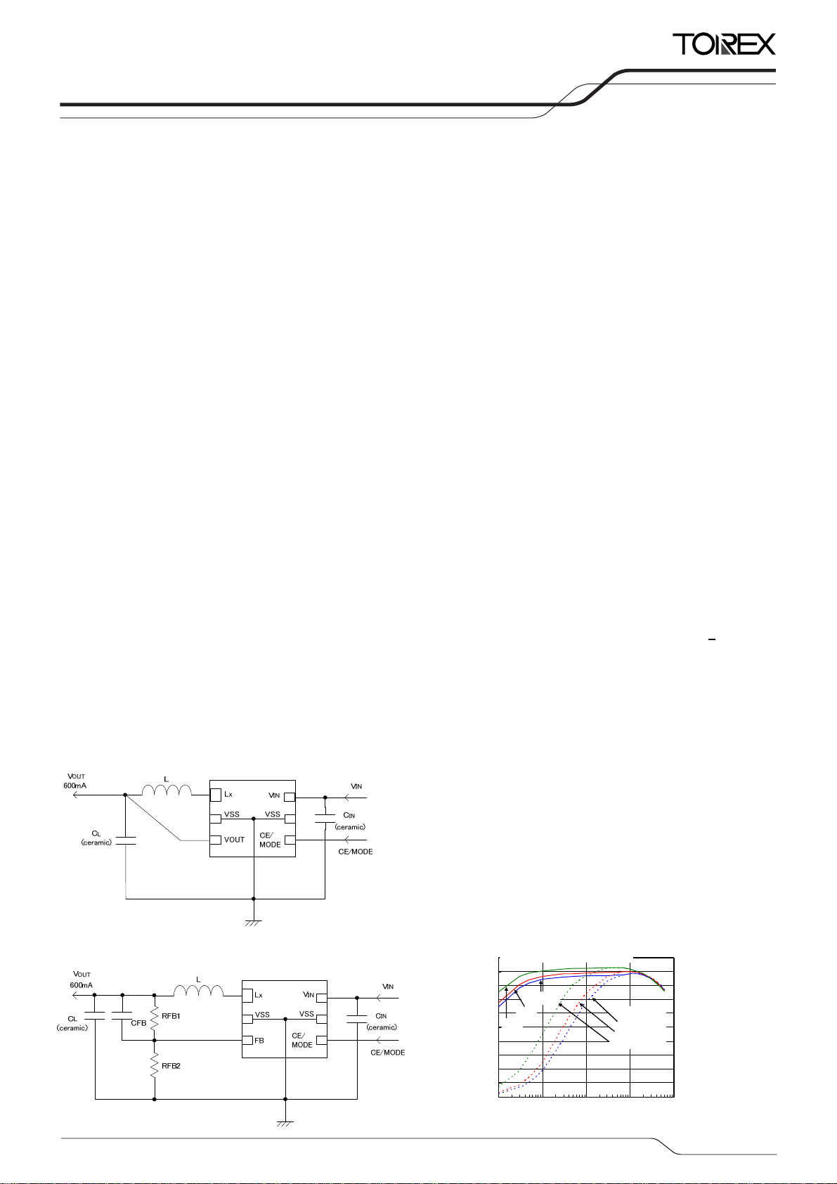
●XC9235/XC9236/XC9237A, B, C, E, G Series (Output Voltage Fixed)
V
OUT
600mA
C
L
(ceramic)
L
Lx
VSS
VOUT
●XC9235/XC9236/XC9237D, F Series (Output Voltage External Setting)
<Setting for Output Voltage>
Output voltage can be set externally by adding two resistors to the FB pin. The output voltage is calculated by the R
R
value. The total of R
FB2
Output voltages can be set in the range of 0.9V to 0.6V by use of 0.8V ± 2.0% reference voltage. However, when input
voltage (V
) is lower than the setting output voltage, output voltage (V
IN
V
OUT
=0.8 × (R
The value of the phase compensation speed-up capacitor C
f
<10kHz. For optimization, f
ZFB
and R
FB1
FB1+RFB2
is usually selected less than 1MΩ.
FB2
)/R
FB2
can be adjusted in the range of 1kHz to 20kHz depending on the inductance L and
ZFB
V
VSS
CE/
MODE
IN
Series
(cera mic)
●f
IN
V
C
IN
CE/ MO DE
OUT
is calculated by the formula of f
FB
=3.0MHz
OSC
L:
CIN:
CL:
●f
=1.2MHz
OSC
L:
CIN:
CL:
) can not be higher than the input voltage (VIN).
1.5μH
4.7μF
10μF
4.7μH
4.7μF
10μF
(NR3015, TAIYO YUDEN)
(Ceramic)
(Ceramic)
(NR4018, TAIYO YUDEN)
(Ceramic)
(Ceramic)
= 1/(2×π×CFB×R
ZFB
the load capacitance CL which are used.
【Formula】
When R
=470kΩ and R
FB1
=150k, V
FB2
=0.8 × (470k+150k) / 150k=3.3V
OUT1
【Example】
V
RFB1 RFB2 CFB V
OUT
(V)
(kΩ) (kΩ)
(pF) (V)
RFB1 RFB2 CFB
OUT
(kΩ) (kΩ)
(pF)
0.9 100 820 150 2.5 510 240 100
1.2 150 300 100 3.0 330 120 150
1.5 130 150 220 3.3 470 150 100
1.8 300 240 150 4.0 120 30 470
FB1
FB1
and
) with
12/33

XC9235/XC9236/XC9237
Series
■OPERATIONAL DESCRIPTION
The XC9235/XC9236/XC9237 series consists of a reference voltage source, ramp wave circuit, error amplifier, PWM
comparator, phase compensation circuit, output voltage adjustment resistors, P-channel MOS driver transistor, N-channel MOS
switching transistor for the synchronous switch, current limiter circuit, UVLO circuit and others. (See the block diagram
above.) The series ICs compare, using the error amplifier, the voltage of the internal voltage reference source with the feedback
voltage from the V
amplifier output, to input a signal to the PWM comparator to determine the turn-on time during PWM operation. The PWM
comparator compares, in terms of voltage level, the signal from the error amplifier with the ramp wave from the ramp wave
circuit, and delivers the resulting output to the buffer driver circuit to cause the Lx pin to output a switching duty cycle. This
process is continuously performed to ensure stable output voltage. The current feedback circuit monitors the P-channel MOS
driver transistor current for each switching operation, and modulates the error amplifier output signal to provide multiple
feedback signals. This enables a stable feedback loop even when a low ESR capacitor such as a ceramic capacitor is used
ensuring stable output voltage.
<Reference Voltage Source>
The reference voltage source provides the reference voltage to ensure stable output voltage of the DC/DC converter.
<Ramp Wave Circuit>
The ramp wave circuit determines switching frequency. The frequency is fixed internally and can be selected from 1.2MHz or
3.0MHz. Clock pulses generated in this circuit are used to produce ramp waveforms needed for PWM operation, and to
synchronize all the internal circuits.
<Error Amplifier>
The error amplifier is designed to monitor output voltage. The amplifier compares the reference voltage with the feedback
voltage divided by the internal split resistors, R1 and R2. When a voltage lower than the reference voltage is fed back, the
output voltage of the error amplifier increases. The gain and frequency characteristics of the error amplifier output are fixed
internally to deliver an optimized signal to the mixer.
<Current Limit>
The current limiter circuit of the XC9235/XC9236/XC9237 series monitors the current flowing through the P-channel MOS
driver transistor connected to the Lx pin, and features a combination of the current limit mode and the operation suspension
mode.
① When the driver current is greater than a specific level, the current limit function operates to turn off the pulses from the Lx
pin at any given timing.
② When the driver transistor is turned off, the limiter circuit is then released from the current limit detection state.
③ At the next pulse, the driver transistor is turned on. However, the transistor is immediately turned off in the case of an over
current state.
④ When the over current state is eliminated, the IC resumes its normal operation.
The IC waits for the over current state to end by repeating the steps ① through ③. If an over current state continues for a
few ms and the above three steps are repeatedly performed, the IC performs the function of latching the OFF state of the
driver transistor, and goes into operation suspension mode. Once the IC is in suspension mode, operations can be
resumed by either turning the IC off via the CE/MODE pin, or by restoring power to the V
not mean a complete shutdown, but a state in which pulse output is suspended; therefore, the internal circuitry remains in
operation. The current limit of the XC9235/XC9236/XC9237 series can be set at 1050mA at typical. Besides, care must
be taken when laying out the PC Board, in order to prevent misoperation of the current limit mode. Depending on the state
of the PC Board, latch time may become longer and latch operation may not work. In order to avoid the effect of noise, the
board should be laid out so that input capacitors are placed as close to the IC as possible.
OUT pin through split resistors, R1 and R2. Phase compensation is performed on the resulting error
pin. The suspension mode does
IN
Limit<#ms
Limit>#ms
ILx
V
VCE
OUT
Lx
Restart
VIN
13/33
I
LIM
0mA
VSS

XC9235/XC9236/XC9237
■OPERATIONAL DESCRIPTION (Continued)
<Short-Circuit Protection>
The short-circuit protection circuit monitors the internal R1 and R2 divider voltage from the V
the block diagram shown in the previous page). In case where output is accidentally shorted to the Ground and when
the FB point voltage decreases less than half of the reference voltage (Vref) and a current more than the I
the Pch MOS driver transistor, the short-circuit protection quickly operates to turn off and to latch the driver transistor.
For the D/E/F/G series, it does not matter how much the current limit, once the FB voltage become less than the
quarter of reference voltage (V
latch mode, the operation can be resumed by either turning the IC off and on via the CE/MODE pin, or by restoring
power supply to the VIN pin.
When sharp load transient happens, a voltage drop at the V
short circuit protection may operate in the voltage higher than 1/2 V
<UVLO Circuit>
When the V
prevent false pulse output caused by unstable operation of the internal circuitry. When the V
or higher, switching operation takes place. By releasing the UVLO function, the IC performs the soft start function to
initiate output startup operation. The soft start function operates even when the VIN pin voltage falls momentarily below
the UVLO operating voltage. The UVLO circuit does not cause a complete shutdown of the IC, but causes pulse output to
be suspended; therefore, the internal circuitry remains in operation.
<PFM Switch Current>
In PFM control operation, until coil current reaches to a specified level (I
on. In this case, time that the Pch MOS driver transistor is kept on (TON) can be given by the following formula.
TON= L×IPFM / (VIN-VOUT) →IPFM①
< PFM Duty Limit >
In PFM control operation, the PFM duty limit (
duty increases (e.g. the condition that the step-down ratio is small), it’s possible for Pch MOS driver transistor to be turned
off even when coil current doesn’t reach to IPFM. →IPFM②
IN pin voltage becomes 1.4V or lower, the Pch MOS driver transistor output driver transistor is forced OFF to
), the short-circuit protection operates to latch the Pch MOS driver transistor. In
REF
Series
DTY
LIMIT_PFM
pin (refer to FB point in
OUT
flows to
LIM
is propagated to the FB point through CFB, as a result,
OUT
) is set to 200% (TYP.). Therefore, under the condition that the
voltage.
OUT
pin voltage becomes 1.8V
IN
PFM), the IC keeps the Pch MOS driver transistor
14/33

XC9235/XC9236/XC9237
■OPERATIONAL DESCRIPTION (Continued)
<CL High Speed Discharge>
XC9235B(C)(D)(E)(F)(G)/ XC9236B(C)(D)(E)(F)(G)/ XC9237B(C)(D)(E)(F)(G) series can quickly discharge the electric
charge at the output capacitor (C
inputted via the Nch MOS switch transistor located between the LX pin and the VSS pin. When the IC is disabled, electric
charge at the output capacitor (C
output capacitor (C
of a CL auto-discharge resistance value [R] and an output capacitor value (CL) as τ(τ=C x R), discharge time of the
output voltage after discharge via the N channel transistor is calculated by the following formulas.
V = V
x e
OUT(E)
V : Output voltage after discharge
V
: Output voltage
OUT(E)
t: Discharge time,
τ: C x R
C= Capacitance of Output capacitor (CL)
R= C
) is set by the CL auto-discharge resistance (R) and the output capacitor (CL). By setting time constant
L
–t/
τ
or t=τln (V
auto-discharge resistance
L
) when a low signal to the CE pin which enables a whole IC circuit put into OFF state, is
L
) is quickly discharged so that it may avoid application malfunction. Discharge time of the
L
/ V)
OUT(E)
Series
Output Voltage Dischage Characteristics
Rdischg
100
90
80
70
60
50
40
30
20
10
0
0 102030405060708090100
= 300Ω TYP
()
CL=10uF
CL=20uF
CL=50uF
Discharge Time t (ms)
15/33

p
XC9235/XC9236/XC9237
Series
■OPERATIONAL DESCRIPTION (Continued)
<CE/MODE Pin Function>
The operation of the XC9235/XC9236/XC9237 series will enter into the shut down mode when a low level signal is input to the
CE/MODE pin. During the shutdown mode, the current consumption of the IC becomes 0μA (TYP.), with a state of high
impedance at the Lx pin and V
input to the CE/MODE pin is a CMOS input and the sink current is 0μA (TYP.).
●XC9235/XC9236 series - Examples of how to use CE/MODE pin
(A)
SW_CE
ON Stand-by
OFF Operation
(B)
SW_CE
ON Operation
OFF Stand-by
●XC9237 series - Exam
(A)
SW_CE SW_PWM/PFM
ON * PWM/PFM Automatic Switching Control
OFF ON PWM Control
OFF OFF Stand-by
(B)
SW_CE SW_PWM/PFM
ON * Stand-by
OFF ON PWM Control
OFF OFF PWM/PFM Automatic Switching Control
Intermediate voltage can be generated by RM1 and RM2. Please set the value of each R1, R2, RM1, RM2 from
few hundreds kΩ to few hundreds MΩ. For switches, CPU open-drain I/O port and transistor can be used.
STATUS
STATUS
OUT pin. The IC starts its operation by inputting a high level signal to the CE/MODE pin. The
(A)
(B)
les of how to use CE/MODE pin
STATUS
STATUS
(A)
(B)
16/33

XC9235/XC9236/XC9237
Series
■OPERATIONAL DESCRIPTION (Continued)
<Soft Start>
Soft start time is available in two options via product selection.
The A,C,D,and E types of XC9235/XC9236/XC9237 series provide 1.0ms (TYP).
The B,F, and G types of XC9235/ XC9236/XC9237 series provide 0.25ms (TYP). However, for the D/F the soft-start time can
be set by the external components. Soft start time is defined as the time interval to reach 90% of the output voltage from the
time when the CE pin is turned on.
0V
V
CEH
V
OUT
0V
■FUNCTION CHART
VOLTAGE LEVEL
L Level
(*1)
(*2)
(*3)
Stand-by Stand-by Stand-by
VCE/
– 0.25V < VCE/
IN
VCE/
MODE
H Level
M Level
Note on CE/MODE pin voltage level range
(*1) H level: 0.65V <
H level: V
(*2) M level: 0.65V < VCE/
(*3) L level: 0V <
XC9235 XC9236 XC9237
Synchronous
PWM Fixed Control
━ ━
< 6.0V (for XC9235/XC9236)
MODE
MODE
< VIN - 1.0V (for XC9237)
MODE
< 0.25V
< V
IN
(for XC9237)
t
SS
OPERATIONAL STATES CE/MODE
Synchronous
PWM/PFM
Automatic Switching
Synchronous
PWM/PFM
Automatic Switching
Synchronous
PWM Fixed Control
90% of setting voltage
17/33

XC9235/XC9236/XC9237
■NOTE ON USE
1. The XC9235/XC9236/XC9237 series is designed for use with ceramic output capacitors. If, however, the potential
difference is too large between the input voltage and the output voltage, a ceramic capacitor may fail to absorb the resulting
high switching energy and oscillation could occur on the output. If the input-output potential difference is large, connect an
electrolytic capacitor in parallel to compensate for insufficient capacitance.
2. Spike noise and ripple voltage arise in a switching regulator as with a DC/DC converter. These are greatly influenced by
external component selection, such as the coil inductance, capacitance values, and board layout of external components.
Once the design has been completed, verification with actual components should be done.
3. Depending on the input-output voltage differential, or load current, some pulses may be skipped, and the ripple voltage may
increase.
4. When the difference between V
possibility that some cycles may be skipped completely.
5. When the difference between V
there is the possibility that some cycles may be skipped completely.
6. With the IC, the peak current of the coil is controlled by the current limit circuit. Since the peak current increases when
dropout voltage or load current is high, current limit starts operation, and this can lead to instability. When peak current
becomes high, please adjust the coil inductance value and fully check the circuit operation. In addition, please calculate
the peak current according to the following formula:
Ipk = (V
L: Coil Inductance Value
f
7. When the peak current which exceeds limit current flows within the specified time, the built-in Pch MOS driver transistor
turns off. During the time until it detects limit current and before the built-in transistor can be turned off, the current for limit
current flows; therefore, care must be taken when selecting the rating for the external components such as a coil.
8. When V
9. Care must be taken when laying out the PC Board, in order to prevent misoperation of the current limit mode. Depending
on the state of the PC Board, latch time may become longer and latch operation may not work. In order to avoid the effect of
noise, the board should be laid out so that input capacitors are placed as close to the IC as possible.
10. Use of the IC at voltages below the recommended voltage range may lead to instability.
11. This IC should be used within the stated absolute maximum ratings in order to prevent damage to the device.
12. When the IC is used in high temperature, output voltage may increase up to input voltage level at no load because of the
leak current of the driver transistor.
13. The current limit is set to 1350mA (MAX.)
①Current flows into Pch MOS driver transistor to reach the current limit (I
②The current of ILIM or more flows since the delay time of the circuit occurs during from the detection of the current limit to
③Because of no potential difference at both ends of the coil, the time rate of coil current becomes quite small.
④Lx oscillates very narrow pulses by the current limit for several ms.
⑤The circuit is latched, stopping its operation.
IN - VOUT) x OnDuty / (2 x L x f
: Oscillation Frequency
OSC
IN is less than 2.4V, limit current may not be reached because voltage falls caused by ON resistance.
current limit functions while the VOUT pin is shorted to the GND pin, when Pch MOS driver transistor is ON, the potential
difference for input voltage will occur at both ends of a coil. For this, the time rate of coil current becomes large. By
contrast, when Nch MOS driver transistor is ON, there is almost no potential difference at both ends of the coil since the
OUT pin is shorted to the GND pin. Consequently, the time rate of coil current becomes quite small. According to the
V
repetition of this operation, and the delay time of the circuit, coil current will be converged on a certain current value,
exceeding the amount of current, which is supposed to be limited originally. Even in this case, however, after the over
current state continues for several ms, the circuit will be latched. A coil should be used within the stated absolute
maximum rating in order to prevent damage to the device.
OFF of Pch MOS driver transistor.
IN and VOUT is large in PWM control, very narrow pulses will be outputted, and there is the
IN and VOUT is small, and the load current is heavy, very wide pulses will be outputted and
OSC
Series
) + IOUT
at typical. However, the current of 1350mA or more may flow. In case that the
LIM).
18/33
XC9235/XC9236/XC9237
Series
■NOTE ON USE (Continued)
14. In order to stabilize VIN’s voltage level and oscillation frequency, we recommend that a by-pass capacitor (CIN) be
connected as close as possible to the V
15. High step-down ratio and very light load may lead an intermittent oscillation.
16. During PWM / PFM automatic switching mode, operating may become unstable at transition to continuous mode.
Please verify with actual parts.
IN & VSS pins.
17. Please note the inductance value of the coil. The IC may enter unstable operation if the combination of ambient
temperature, setting voltage, oscillation frequency, and L value are not adequate.
In the operation range close to the maximum duty cycle, The IC may happen to enter unstable output voltage operation
even if using the L values listed below.
<External Components>
18. It may happen to enter unstable operation when the IC goes into continuous operation mode under the condition of large
input-output voltage difference. Care must be taken with the actual design unit.
●The Range of L Value
f
V
OSC
3.0MHz
1.2MHz
*When a coil less value of 4.7μH is used at
f
=1.2MHz or when a coil less value of 1.5μH is
OSC
used at f
reach the current limit ILMI. In this case, it may
happen that the IC can not provide 600mA output
current.
0.8V<V
=3.0MHz, peak coil current more easily
OSC
L Value
OUT
<4.0V 1.0μH~2.2μH
OUT
V
≦2.5V 3.3μH~6.8μH
OUT
2.5V<V
4.7μH~6.8μH
OUT
<External Components>
19/33

XC9235/XC9236/XC9237
Series
■NOTE ON USE (Continued)
●Instructions of pattern layouts
1. In order to stabilize VIN voltage level, we recommend that a by-pass capacitor (CIN) be connected as close as possible to
the VIN & VSS pins.
2. Please mount each external component as close to the IC as possible.
3. Wire external components as close to the IC as possible and use thick, short connecting traces to reduce the circuit
impedance.
4. Make sure that the PCB GND traces are as thick as possible, as variations in ground potential caused by high ground
currents at the time of switching may result in instability of the IC.
5. This series’ internal driver transistors bring on heat because of the output current and ON resistance of driver transistors.
XC9235/9236/9237A, B, C (Output Voltage Fixed) XC9235/9236/9237A, B, C, E, G (Output Voltage Fixed)
CL
For the VIN, VOUT, VSS, CE, please put the wire.
Inductor
Inductor
Inductor
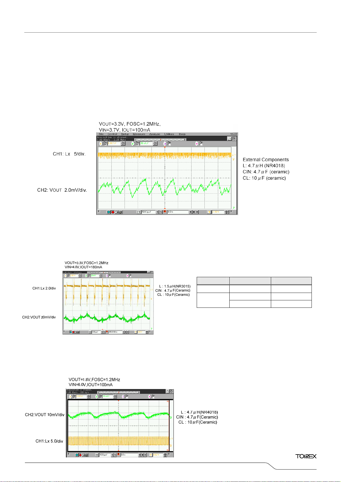
Inductor
For the VIN, VOUT, VSS, CE, please put the wire.
XC9235/9236/9237D, F (Output Voltage External Setting)
Chip
Chip
Resistance
Resistance
Inductor
Inductor
20/33
For the VIN, VOUT, VSS, CE, please put the wire.

■TEST CIRCUITS
< Circuit No.1 >
・A/B/C/E/G series ・D/F series
A
CIN
VIN Lx
CE/MODE VOUT
VSS
Wave Form Measure Point
L
CL
RL
V
※ Exte rnal Components
L : 1.5uH(NR3015) 3.0MHz
4.7uH(NR4018) 1.2MHz
CIN : 4.7μF(ceramic)
CL :10μF(ceramic)
< Circuit No.2 >
A
1uF
VIN Lx
VSS
VOUT
(FB)
CE/MODE
< Circuit No.3 >
< Circuit No.4 >
< Circuit No.5 >
1uF
VIN Lx
VSS
VOUT
(FB)
CE/MODE
V
100mA
ON resistance = (VIN-VLx)/100mA
< Circuit No.6 >
1uF
VIN Lx
VSS
VOUT
(FB)
CE/MODE
Wave Form Measure Point
V
ILIM
< Circuit No.7 >
< Circuit No.8 >
1uF
VIN Lx
VSS
VOUT
(FB)
CE/MODE
ILx
A
< Circuit No.9 >
A
※ Exte rnal Components
L : 1.5μH(NR4018) 3.0MHz V
: 4.7μH (NR3015) 1.2MH z
CIN : 4.7μF
CL : 10μF
R1 : 150kΩ
R2 : 300kΩ
Cfb : 120pF
1uF
A
VIN Lx
CIN
CE/MODE
1uF
ICEH
A
ICEL
1uF
CIN
VIN Lx
CE/MODE
VIN Lx
CE/MODE
VIN Lx
CE/MODE
VIN Lx
CE/MODE
VSS
OUT=VFB×(R1+R2)/R2
VSS
VSS
VSS
VSS
XC9235/XC9236/XC9237
Series
Wave Form Measure Point
FB
VOUT
(FB)
L
R1
R2
Wave Form Measure Point
Rpulldown
200Ω
IOUT
Cfb
CL
V
RL
A
VOUT
(FB)
Wave Form Measure Point
VOUT
(FB)
VOUT
(FB)
Ilat
Rpulldown
1Ω
21/33

)
)
XC9235/XC9236/XC9237
Series
■TYPICAL PERFORMANCE CHARACTERISTICS
(1) Efficiency vs. Output Current
Efficiency: EFFI (%)
Efficency:EFFI(%
L=4.7μH (NR4018), CIN=4.7μF, C L = 1 0μF
PWM/ PFM A ut omat ic Sw i t c h ing Contr ol
100
90
80
70
60
50
40
30
20
10
0
VIN= 4.2V
3.6V
2.4V
0.1 1 10 100 1000
(2) Output Voltage vs. Output Current
L=4.7μH (NR4018), CIN=4.7μF, C L = 1 0μF
2.1
XC9237A18C
PWM Control
VIN= 4.2V
3.6V
2.4V
Output Current: IOUT (mA)
Output Current:IOUT(mA)
XC9237A18C
L=1.5μH (NR3015), CIN=4.7μF, C L = 1 0μF
PWM/ PFM A ut omat ic Sw i t c h ing Contr ol
100
90
80
70
60
50
40
Efficency:EFFI( %
30
Efficiency: EFFI (%)
20
10
0
0.1 1 10 100 1000
2.1
VIN= 4.2V
3.6V
2.4V
L=1.5μH (NR3015), CIN=4.7μF, C L = 1 0μF
XC9237A18D
PWM Control
VIN= 4.2V
3.6V
2.4V
Output Current: IOUT (mA)
Output Current:IOUT(mA)
XC9237A18D
2.0
1.9
1.8
1.7
Output Voltage: VOUT (V)
Output Voltage:Vout(V)
1.6
1.5
0.1 1 10 100 1000
PWM/ PFM A ut omat ic Sw i t c h ing Contr ol
Output Current: IOUT (mA)
Output Current:IOUT(mA)
VIN=4.2V,3.6V ,2.4V
PWM C o n t r ol
(3) Ripple Voltage vs. Output Current
L=4.7μH (NR4018), CIN=4.7μF, C L = 1 0μF
100
80
60
PWM Control
40
VIN=4.2V,3.6V ,2.4V
Ripple Voltage:Vr(mV)
Ripple Voltage: Vr (mV)
20
XC9237A18C
PWM/ PFM A ut o ma t i c
Sw itching Control
VIN=4.2V
3.6V
2.4V
2.0
1.9
1.8
1.7
Output Voltage:Vout(V)
1.6
1.5
0.1 1 10 100 1000
100
80
60
40
Ripple Voltage:Vr(mV)
Ripple Voltage: Vr (mV)
20
PWM/PFM Automatic Sw itching Control
Output Current: IOUT (mA)
Output Current:IOUT(mA)
L=1.5μH (NR3015), CIN=4.7μF, C L = 1 0μF
PWM Control
VIN=4.2V,3.6V ,2.4V
VIN=4.2V,3.6V ,2.4V
PWM Control
XC9237A18D
PWM/PFM Automatic
Sw itching Control
VIN=4.2V
3.6V
2.4V
0
0.1 1 10 100 1000
Output Current: IOUT (mA)
Output Current:IOUT(mA)
0
0.1 1 10 100 1000
Output Current: IOUT (mA)
Output Current:IOUT(mA)
22/33

)
)
XC9235/XC9236/XC9237
■TYPICAL PERFORMANCE CHARACTERISTICS (Continued)
(4) Oscillation Frequency vs. Ambient Temperature
L=4.7μH (NR4018), CIN=4.7μF, C L = 1 0μF
1.5
1.4
1.3
1.2
1.1
1.0
0.9
Oscillation Frequency: FOSC (MHz)
Oscillation Frequency : FOSC(MHz)
0.8
-50 -25 0 25 50 75 100
XC9237A18C
VIN=3.6V
Ambient Temperature: Ta (℃)
Ambient Temperature: Ta (℃)
L=1.5μH (NR3015), CIN=4.7μF, C L = 1 0μF
3.5
3.4
3.3
3.2
3.1
3.0
2.9
2.8
2.7
Oscillation Frequency: FOSC (MHz)
Oscillation Frequency : FOSC(MHz)
2.6
2.5
-50 -25 0 25 50 75 100
(5) Supply Current vs. Ambient Temperature
40
35
30
25
20
15
10
Supply Current: IDD (μA)
Supply Current : IDD (μA
5
0
-50 -25 0 25 50 75 100
VIN=2.0V
XC9237A18C
VIN=6.0V
VIN=4.0V
Ambient Temperature: Ta (℃)
Ambient Temperature: Ta (℃)
40
35
30
25
20
15
10
Supply Current : IDD (μA
Supply Current: IDD (μA)
VIN=2.0V
5
0
-50-250 255075100
(6) Output Voltage vs. Ambient Temperature (7) UVLO Voltage vs. Ambient Temperature
2.1
2.0
XC9237A18D
1.8
1.5
XC9237A18D
VIN=3.6V
Ambient Temperature: Ta (℃)
Ambient Temperature: Ta (℃)
XC9237A18D
VIN=4.0V
Ambient Temperature: Ta (℃)
Ambient Temperature: Ta (℃)
XC9237A18D
VIN=6.0V
CE=V IN
Series
1.9
1.8
1.7
Output Voltage: VOUT (V)
Output Voltage : VOUT (V)
1.6
1.5
-50-250 255075100
VIN=3.6V
Ambient Temperature: Ta (℃)
Ambient Temperature: Ta (℃)
1.2
0.9
0.6
UVLO Voltage: UVLO (V)
UVLO Voltage : UVLO (V)
0.3
0.0
-50-250 255075100
Ambient Temperature: Ta (℃)
Ambient Temperature: Ta (℃)
23/33
)
)
)
XC9235/XC9236/XC9237
Series
■TYPICAL PERFORMANCE CHARACTERISTICS (Continued)
(8) CE "H" Voltage vs. Ambient Temperature (9) CE "L" Voltage vs. Ambient Temperature
1.0
0.9
0.8
0.7
0.6
0.5
0.4
0.3
CE "H " Voltage : VC EH ( V
CE “H” Voltage: VCEH (V)
0.2
0.1
0.0
-50 -25 0 25 50 75 100
XC9237A18D
VIN=5.0V
VIN=2.4V
Ambient Temperature: Ta (℃)
Ambient Temperature: Ta (℃)
VIN=3.6V
1.0
0.9
0.8
0.7
0.6
0.5
0.4
0.3
CE “L” Voltage: VCEL (V)
CE "L" Voltage : VCEL (V)
0.2
0.1
0.0
-50 -25 0 25 50 75 100
XC9237A18D
VIN=5.0V
VIN=3.6V
VIN=2.4V
Ambient Temperature: Ta (℃)
Ambient Temperature: Ta (℃)
(10) Soft Start Time vs. Ambient Temperature
L=4.7μH (NR4018), CIN=4.7μF, C L = 1 0μF
5
XC9237A18C
L=1.5μH (NR3015), CIN=4.7μF, C L = 1 0μF
XC9237A18D
5
4
3
2
Soft Start Time: TSS (ms)
Soft Start Time : TSS (ms
1
0
-50-25 0 255075100
VIN=3.6V
Ambient Temperature: Ta (℃)
Ambient Temperature: Ta (℃)
4
3
2
Soft Start Time: TSS (ms)
Soft Start Time : TSS (ms
1
0
-50 -25 0 25 50 75 100
VIN=3.6V
Ambient Temperature: Ta (℃)
Ambient Temperature: Ta (℃)
(11) "Pch / Nch" Driver on Resistance vs. Input Voltage
1.0
0.9
0.8
0.7
0.6
0.5
0.4
0.3
0.2
Lx SW ON Res istanc e:RLxH,RLxL ( Ω)
0.1
Lx SW ON Resistance: RLxH, RLxL (Ω)
0.0
0123456
XC9237A18D
Nch on Resistance
Pch on Resistanc e
Input Voltage : VIN (V)
Input Voltage: VIN (V)
24/33
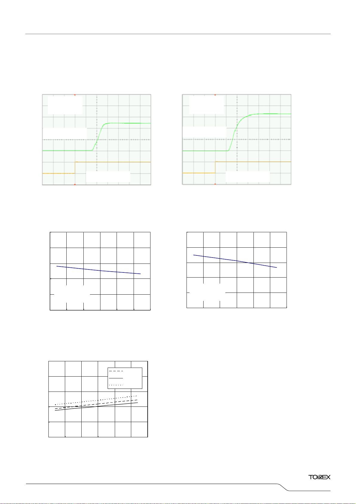
A
A
XC9235/XC9236/XC9237
■TYPICAL PERFORMANCE CHARACTERISTICS (Continued)
(12) XC9235B/36B/37B Rise Wave Form
L=4.7μH (NR4018), CIN=4.7μF, C L = 1 0μF
XC9237B12C
L=1.5μH (NR3015), CIN=4.7μF, C L = 1 0μF
XC9237B33D
Series
VIN=5.0V
IOUT=1.0m
VOUT:0.5V/div
100μs/div 100μs/div
(13) XC9235B/36B/37B Soft-Start Time vs. Ambient Temperature
XC9237B12C XC9237B33D
L=4.7μH(NR4018), CIN=4.7μF, C L = 1 0 μF L=1.5μH(NR3015), CIN=4.7μF, C L = 10 μF
500
400
300
VIN=5.0V
IOUT=1.0m
VOUT:1.0V/div
CE:0.0V⇒1.0V CE:0.0V⇒1.0V
500
400
300
200
Soft Start Time :TSS (μs)
VIN=5.0V
IOUT=1. 0m A
100
0
-50 -25 0 25 50 75 100
Ambient Temperature: Ta(℃)
200
VIN=5.0V
Soft Start Time :TSS (μs)
IOUT=1.0m A
100
0
-50 -25 0 25 50 75 100
Ambient Temperature: Ta(℃)
(14) XC9235B/36B/37B CL Discharge Resistance vs. Ambient Temperature
XC9237B33D
600
500
400
300
200
CL Discharge Resistance: (Ω)
100
-50 -25 0 25 50 75 100
Ambient Temperature: Ta (℃)
VIN=6.0V
VIN=4.0V
VIN=2.0V
25/33

XC9235/XC9236/XC9237
Series
■TYPICAL PERFORMANCE CHARACTERISTICS (Continued)
(15) Load Transient Response
XC9237A18C
L=4.7μH (NR4018), C
=3.6V, VCE=VIN (PWM/PFM Automatic Switching Control)
V
IN
=1mA → 100mA I
I
OUT
1ch: I
V
: 50mV/div V
OUT
I
=100mA → 1mA I
OUT
1ch: I
V
: 50mV/div V
OUT
1ch: I
OUT
2ch 2ch
1ch: I
OUT
2ch 2ch
=4.7μF (ceramic), CL=10μF (ceramic), Topr=25℃
IN
50μs/div 50μs/div
200μs/div 200μs/div
=1mA → 300mA
OUT
OUT
: 50mV/div
OUT
=300mA → 1mA
OUT
OUT
: 50mV/div
OUT
26/33

XC9235/XC9236/XC9237
■TYPICAL PERFORMANCE CHARACTERISTICS (Continued)
(15) Load Transient Response (Continued)
XC9237A18C
L=4.7μH (NR4018), C
=3.6V, VCE=1.8V (PWM Control)
V
IN
=1mA → 100mA I
I
OUT
1ch: I
1ch: I
OUT
2ch 2ch
V
: 50mV/div V
OUT
I
=100mA → 1mA I
OUT
1ch: I
1ch: I
OUT
2ch 2ch
V
: 50mV/div V
OUT
=4.7μF (ceramic), CL=10μF (ceramic), Topr=25℃
IN
50μs/div 50μs/div
200μs/div 200μs/div
=1mA → 300mA
OUT
OUT
: 50mV/div
OUT
=300mA → 1mA
OUT
OUT
: 50mV/div
OUT
Series
27/33

XC9235/XC9236/XC9237
Series
■TYPICAL PERFORMANCE CHARACTERISTICS (Continued)
(15) Load Transient Response (Continued)
XC9237A18D
L=1.5μH (NR3015), C
=3.6V, VCE=VIN (PWM/PFM Automatic Switching Control)
V
IN
=1mA → 100mA I
I
OUT
1ch: I
V
: 50mV/div V
OUT
I
=100mA → 1mA I
OUT
1ch: I
: 50mV/div V
V
OUT
1ch: I
OUT
2ch 2ch
1ch: I
OUT
2ch 2ch
=4.7μF (ceramic), CL=10μF (ceramic), Topr=25℃
IN
50μs/div 50μs/div
200μs/div 200μs/div
=1mA → 300mA
OUT
OUT
: 50mV/div
OUT
=300mA → 1mA
OUT
OUT
: 50mV/div
OUT
28/33

XC9235/XC9236/XC9237
■TYPICAL PERFORMANCE CHARACTERISTICS (Continued)
(15) Load Transient Response (Continued)
XC9237A18D
L=1.5μH (NR3015), C
=3.6V, VCE=1.8V (PWM Control)
V
IN
=1mA → 100mA I
I
OUT
1ch: I
V
: 50mV/div V
OUT
I
=100mA → 1mA I
OUT
1ch: I
: 50mV/div V
V
OUT
1ch: I
OUT
2ch 2ch
1ch: I
OUT
2ch 2ch
=4.7μF (ceramic), CL=10μF (ceramic), Topr=25℃
IN
50μs/div 50μs/div
200μs/div 200μs/div
=1mA → 300mA
OUT
OUT
: 50mV/div
OUT
=300mA → 1mA
OUT
OUT
: 50mV/div
OUT
Series
29/33

XC9235/XC9236/XC9237
Series
■PACKAGING INFORMATION
●SOT-25
●USP-6C Reference Pattern Layout
0.05
2.4
0.45
6
5
4
0.05
1.0
0.45
1
2
3
●USP-6C
●USP-6C Reference Metal Mask Design
30/33

■PACKAGING INFORMATION (Continued)
●USP-6EL
* A part of the pin may appear from the side of the package because of it’s
structure, but reliability of the package and strength will not be changed below the
standard.
●USP-6EL Reference Pattern Layout
0.35
0.3750.375
1.5
0.55 0.55
1.1
2.25
XC9235/XC9236/XC9237
●USP-6EL Reference Metal Mask Design
1.4
0.3
0.5
0.30.3
0.9
0.55 0.55
Series
2.2
31/33

XC9235/XC9236/XC9237
■MARKING RULE
●SOT-25
SOT-25
(TOP VIEW)
USP-6C/USP-6EL
(TOP VIEW)
① represent product series
② represents integer number of output voltage and oscillation frequency
●A/B/C/F Series
VOLTAGE (V)
●E/G/D Series
VOLTAGE (V)
③ represents decimal point of output voltage
④⑤ represents production lot number
Order of 01, …09, 10, 11, …99, 0A, …0Z, 1A, …9Z, A0, …Z9, AA, …ZZ.
(G, I, J, O, Q, W excluded)
*No character inversion used.
Series
PRODUCT
SERIES
XC9235 XC9236 XC9237
A 4 5 6
B C D E
C K L M
D K L M
E 4 5 6
F 2 7 B
G C D E
MARK OUTPUT
f
=1.2MHz f
OSC
=3.0MHz
OSC
0.X A F
1.X B H
2.X C K
3.X D L
4.X E M
OUTPUT
f
=1.2MlHz f
OSC
MARK
=3.0MlHz
OSC
0.X N U
1.X P V
2.X R X
3.X S Y
4.X T Z
V
(V) MARK V
OUT
(V) MARK
OUT
X.00 0 X.05 A
X.10 1 X.15 B
X.20 2 X.25 C
X.30 3 X.35 D
X.40 4 X.45 E
X.50 5 X.55 F
X.60 6 X.65 H
X.70 7 X.75 K
X.80 8 X.85 L
X.90 9 X.95 M
32/33
XC9235/XC9236/XC9237
Series
1. The products and product specifications contained herein are subject to change without
notice to improve performance characteristics. Consult us, or our representatives
before use, to confirm that the information in this datasheet is up to date.
2. We assume no responsibility for any infringement of patents, patent rights, or other
rights arising from the use of any information and circuitry in this datasheet.
3. Please ensure suitable shipping controls (including fail-safe designs and aging
protection) are in force for equipment employing products listed in this datasheet.
4. The products in this datasheet are not developed, designed, or approved for use with
such equipment whose failure of malfunction can be reasonably expected to directly
endanger the life of, or cause significant injury to, the user.
(e.g. Atomic energy; aerospace; transport; combustion and associated safety
equipment thereof.)
5. Please use the products listed in this datasheet within the specified ranges.
Should you wish to use the products under conditions exceeding the specifications,
please consult us or our representatives.
6. We assume no responsibility for damage or loss due to abnormal use.
7. All rights reserved. No part of this datasheet may be copied or reproduced without the
prior permission of TOREX SEMICONDUCTOR LTD.
33/33
 Loading...