

100
XC9220/XC9221 Series
ETR0511-011
16V Input Voltage, Step-Down DC/DC Controller ICs.
■GENERAL DESCRIPTION
The XC9220/XC9221 series is a group of multi-purpose step-down DC/DC controller ICs. The ICs enable a high efficiency,
stable power supply with an output current up to 3A to be configured using only a transistor, a coil, a diode, and two capacitors
connected externally. Low ESR capacitors such as a ceramic capacitor can be used as an output capacitor.
The XC9220/XC9221 series has a 0.9V (±1.5%) reference voltage, and using externally connected resistors, the output
voltage can be set freely. With an internal switching frequency of 300kHz and 500kHz 1.0MHz, small external components
can also be used. The XC9220 series is PWM control, and the XC9221 series is PWM/PFM mode, which automatically
switches from PWM to PFM during light loads and high efficiencies can be achieved over a wide range of load conditions.
As for the soft-start time, the XC9220/XC9221A and C series is internally set to 4msec and the XC9220/XC9221B and D
series can be externally set-up. With the built-in UVLO (Under Voltage Lock Out) function, the external P-channel driver
transistor is forced OFF when input voltage becomes 2.3V or lower.
■APPLICATIONS
●Set top boxes
●Digital TVs
●DVD/HDD recorders
●Portable information terminals
●Notebook computers
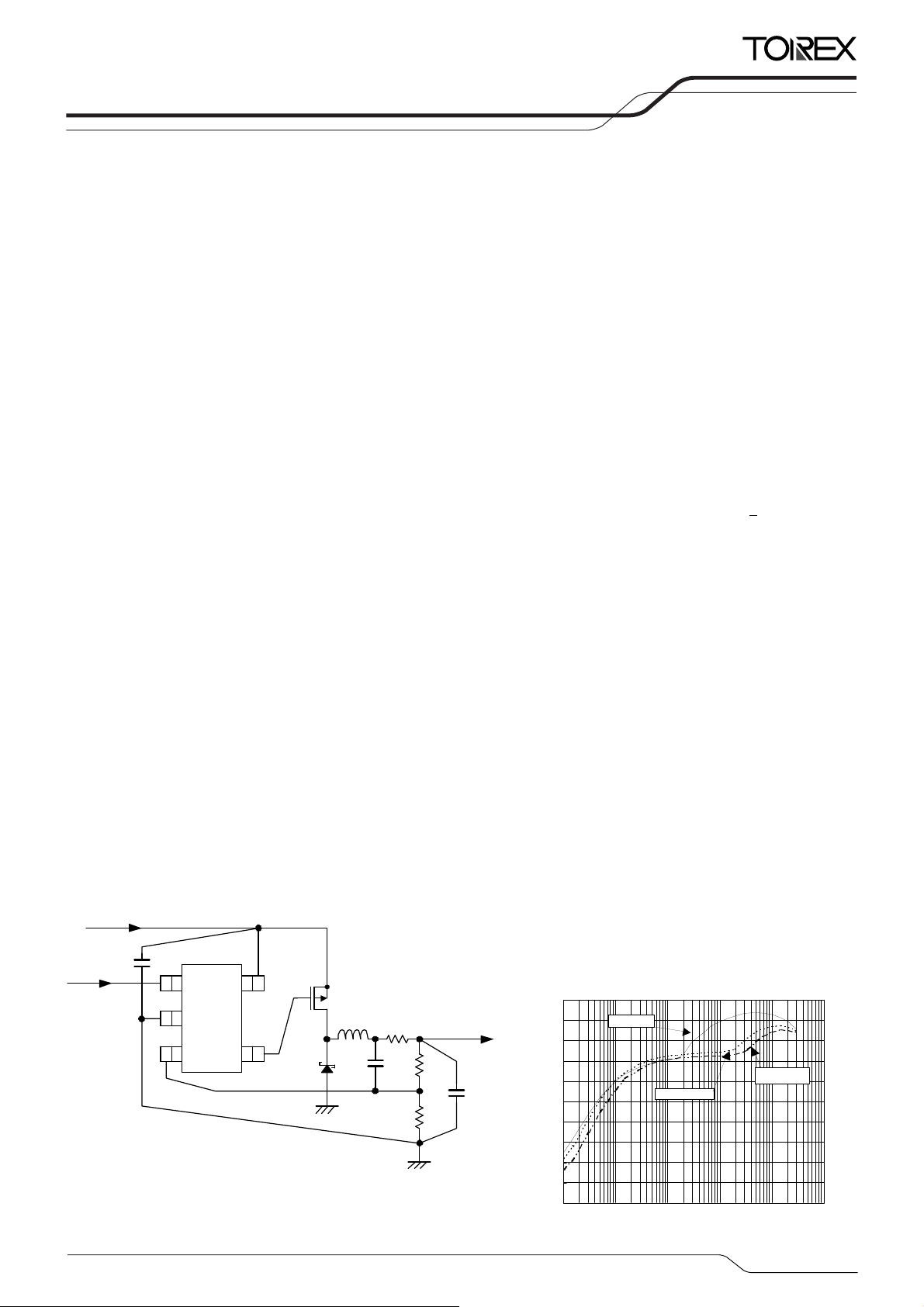
■TYPICAL APPLICATION CIRCUIT
V
IN
C
IN
CE
* RSENSE : Tantalum and electrolytic capac itors can be used, in w hich cas e,
RSENSE becomes unneces sary.
CE GND FB
1 2 3
V
IN
EXT
5 4
SBD
Pc h
MOS FET
L
C
FB
RSENSE
( for ceramic CL )
■FEATURES
Operating Voltage Range : 2.8V ~ 16.0V
Output Voltage Externally Set Range
(V
: 1.2V or more
=0.9V+1.5%)
FB
Output Current : Less than 3.0A
Oscillation Frequency : 300kHz, 500kHz, and 1.0MHz
Control Methods : PWM control (XC9220)
PWM/PFM automatic switching
(XC9221)
Soft-Start Function : 4ms, internally set
Protection Circuits
Low ESR
Capacitor Compatible
(XC9220/XC9221A, 500kHz)
Externally set
(XC9220/XC9221B)
: Integral protection (1.0 ms)
(XC9220/XC9221 Aand B series)
Short-circuit protection
: Ceramic capacitor
Operating Ambient Temperature : - 40℃~ + 85℃
Packages
: SOT-25
USP-6C
Environmentally Friendly :
EU RoHS Compliant, Pb Free
■TYPICAL PERFORMANCE
CHARACTERISTICS
●Efficiency vs. Output Current
XC9221A095MR (VOUT=3.3V, FOSC=500kHz)
PchMOSFET: CPH3308 (SANYO), CDD=1.0μF (ceramic), RIN=10Ω
OUT
V
R
FB1
CL
R
FB2
90
80
70
60
EFFI (%)
50
40
30
Efficienc y
20
10
0
0.1 1 10 100 1000 10000
CIN=47μF (OS-Con), CL=47μF (OS-Con),
L=10μH (CDRH8D43, SUMIDA)
VIN=5.0V
VIN=12 .0V
Output Current IO UT ( m A)
VIN=16 .0V
1/22
XC9220/XC9221 Series
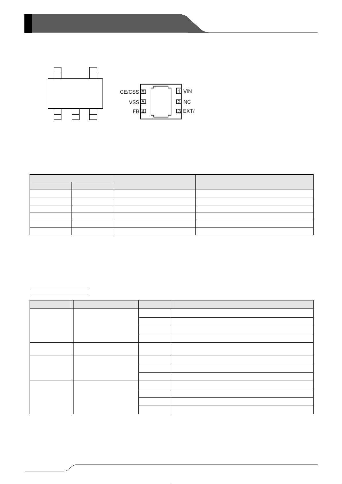
■PIN CONFIGURATION
■PIN ASSIGNMENT
■PRODUCT CLASSIFICATION
●Ordering Information
XC9220①②③④⑤⑥-⑦
XC9221①②③④⑤⑥-⑦
DESIGNATOR ITEM SYMBOL DESCRIPTION
IN
5 4
1 2 3
CE/CSSV
SOT-25
(TOP VIEW)
PIN NUMBER
SOT-25 USP-6C
SS
EXT/V
* The dissipation pad for the USP-6C package
(preliminary) should be solder-plated in
recommended mount pattern and metal
masking so as to enhance mounting strength
and heat release. If the pad needs to be
connected to other pins, it should be
connected to the V
FB
USP-6C
(BOTTOM VIEW)
PIN NAME FUNCTION
1 6 CE/CSS Chip Enable / Soft-Start
2 5 VSS Ground
3 4 FB Output Voltage Sense
4 3 EXT/ External Transistor Drive
- 2 NC No Connection
5 1 VIN Power Supply
(*1)
: PWM control
(*1)
: PWM/PFM automatic switching control
A Soft-start internally set with integral protection function
①
Type of DC/DC Controller
ICs
B Soft-start externally set with integral protection function
C Soft-start internally set without integral protection function
D Soft-start externally set without integral protection function
SS (No.5) pin.
②③ Output Voltage 09 FB Voltage (Fixed)
3 300kHz
④ Oscillation Frequency
5 500kHz
A 1.0MHz
MR SOT-25 (3,000/Reel)
⑤⑥-⑦
(*1)
Packages (Order Unit)
MR-G SOT-25 (3,000/Reel)
ER USP-6C (3,000/Reel)
ER-G USP-6C (3,000/Reel)
(*1)
The “-G” suffix denotes Halogen and Antimony free as well as being fully RoHS compliant.
2/22
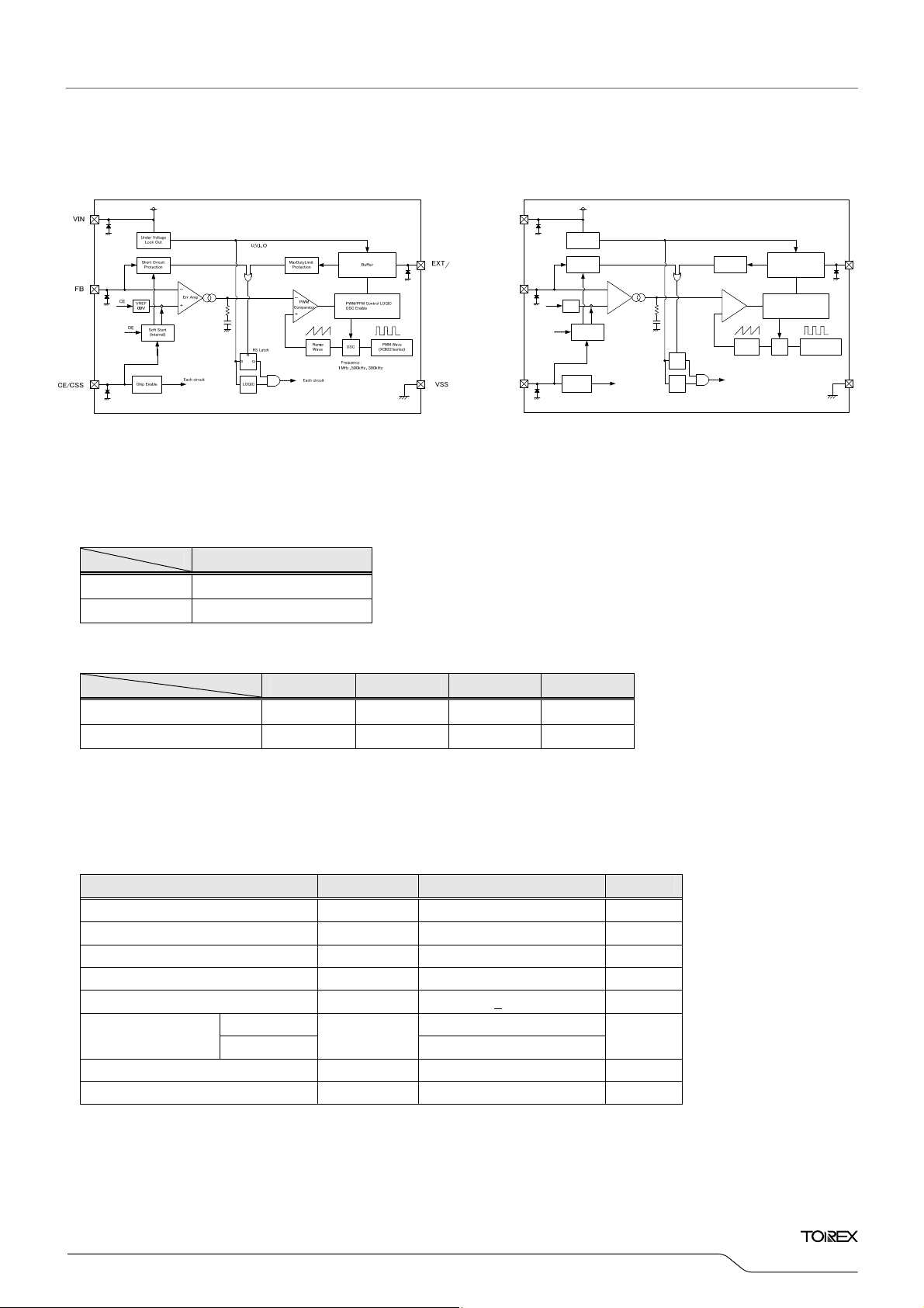
■BLOCK DIAGRAMS
●XC9220/21A and C series ● XC9220/21B and D series
XC9220/XC9221
Series
VIN
FB
CE/CSS
* Diodes inside the circuits are ESD protection diodes and parasitic diodes.
■ FUNCTIONS
CHIP ENABLE
IC OPERATION
H Operation ON
L Operation OFF
PRODUCT TYPE
A B C D
Soft-start externally set No Yes No Yes
Integral protection function Yes Yes No No
■ ABSOLUTE MAXIMUM RATINGS
PAR AMETER SYMBOL RATINGS UNITS
VIN Pin Voltage VIN
FB Pin Voltage VFB
CE/CSS Pin Voltage CE
-0.3 ~ +18.0
-0.3 ~ +18.0
-0.3 ~ +18.0
EXT/ Pin Voltage VEXT - 0.3 ~ VIN + 0.3 V
EXT/ Pin Current IEXT + 100 mA
Power Dissipation
SOT-25 250
USP-6C
Pd
120
Operating Ambient Temperature Topr - 40 ~ + 85
Storage Temperature Tstg - 55 ~ +125
Under Voltag e
Lock Out
Short Circuit
Protection
-
VREF
0.9V
Chip Enable
Soft Start
(internal)
Err Amp
+
Each circuit
CE
OE
U.V.L.O
MaxDutyLimit
Protection
-
PWM
Comparator
+
Ramp
RS Latch
R
Q
S
LOGIC
Wave
Each circuit
Buffer
PWM/PFM Control LOGIC
OSC Enable
OSC
Frequency :
1 MHz, 500 kHz , 300 kHz
PWM Wave
(XC9221series)
EXT
/
VSS
Ta = 25OC
V
V
V
mW
O
C
O
C
3/22
XC9220/XC9221 Series
■ELECTRICAL CHARACTERISTICS
XC9220/XC9221 A and C series
PAR AMETER SYMBOL CONDITIONS MIN. TYP. MAX. UNIT.
FB Voltage VFB 0.8865 0.9000 0.9135 V 2
Input Voltage Range VIN 2.8 - 16.0 V -
UVLO Voltage
(Minimum Operating Voltage)
Supply Current 2 IDD2 VIN=5.0V, FB=1.0V ** μA 1
Stand-by Current ISTB - 0.1 1.0 μA 1
Oscillation Frequency fOSC
Maximum Duty Ratio MAXDTY 100 - - % 2
PFM Duty Ratio PFMDTY No load (XC9221 series only) 15 25 35 % 3
EXT/ High On Resistance REXTBH 6 10 16 Ω 4
EXT/ Low On Resistance REXTBL 6 12 20 Ω 4
Integral Protection Time
(*2)
Short-Circuit Protection VSHORT - - 0.7 V 2
Soft-Start Time tSS ** ms 2
Efficiency (*1) EFFI - 92 - % 3
Temperature Characteristics
CE “High” Level Voltage VCEH 1.2 - - V 2
CE “Low” Level Voltage VCEL - - 0.3 V 3
CE “High” Level Current ICEH VIN=CE=16V - 0.1 - 0.1 μA 1
CE “Low” Level Current ICEL VIN=16V, CE=0V - 0.1 - 0.1 μA 1
FB “High” Level Current IFBH VIN=FB=16V - 0.1 - 0.1 μA 4
FB “Low” Level Current IFBL VIN=16V, FB=0V - 0.1 - 0.1 μA 4
Unless otherwise stated, V
NOTE:
*1: EFFI = { (output voltage) x (output current)} / { (input voltage) x (input current) } x 100
*2: No Integral protection function is available with the XC9220/9221 C series.
** Refer to the CHARACTERISTICS CHART BY OSCILLATION FREQUENCY.
IN=5.0V
VUVLO 1.9 2.3 2.7 V 3
Connected to external
components
tPRO (XC9220/9221 A series) ** ms 2
UVFB FB Voltage
UToprVFB
- +100 -
** kHz 3
ppm
/OC
Ta = 2 5OC
CIRCUIT
2
4/22
■ELECTRICAL CHARACTERISTICS (Continued)
XC9220/XC9221 B and D series
XC9220/XC9221
Series
Ta = 2 5OC
PAR AMETER SYMBOL CONDITIONS MIN. TYP. MAX. UNIT.
CIRCUIT
FB Voltage VFB 0.8865 0.9000 0.9135 V 2
Input Voltage Range VIN 2.8 - 16.0 V -
UVLO Voltage
(Minimum Operating Voltage)
VUVLO 1.9 2.3 2.7 V 3
Supply Current 2 IDD2 VIN=5.0V, FB=1.0V ** μA 1
Stand-by Current ISTB - 0.1 1.0 μA 1
Oscillation Frequency fOSC
Connected to external
components
** kHz 3
Maximum Duty Ratio MAXDTY 100 - - % 2
PFM Duty Ratio PFMDTY No load (XC9221 series only) 15 25 35 % 3
EXT/ High On Resistance REXTBH 6 10 16 Ω 4
EXT/ Low On Resistance REXTBL 6 12 20 Ω 4
Integral Protection Time
(*4)
tPRO (XC9220/9221 B series) ** ms 2
Short-Circuit Protection VSHORT - - 0.7 V 2
Soft-Start Time tSS Connected to RSS and CSS 5.0 10.0 20.0 ms 5
Internal Soft-Start Time (*1) tSS_IN CE=VIN ** ms 2
Efficiency (*2) EFFI - 92 - % 3
Temperature Characteristics
CE “High” Level Voltage
(*3)
UVFB FB Voltage
UToprVFB
- +100 -
VCEH 2.6 - - V 2
ppm
/OC
2
CE “Low” Level Voltage VCEL - - 0.3 V 2
CE “High” Level Current ICEH VIN=CE=16V - 0.1 - 0.1 μA 1
CE “Low” Level Current ICEL VIN=16V, CE=0V - 0.1 - 0.1 μA 1
FB “High” Level Current IFBH VIN=FB=16V - 0.1 - 0.1 μA 4
FB “Low” Level Current IFBL VIN=16V, FB=0V - 0.1 - 0.1 μA 4
Unless otherwise stated, V
External components: C
NOTE:
*1: Internal soft-start time: In case where the U.V.L.O. function operates temporarily due to the power cutoff etc. when an external C
charged (V
internal soft-start time.
*2: EFFI={ (output voltage) x (output current) } / { (input voltage) x (input current) } x 100
*3: The integral latch and short-circuit protection do not function when the CE/C
*4: No Integral protection function is available with the XC9220/XC9221 D series.
** Refer to the CHARACTERISTICS CHART BY OSCILLATION FREQUENCY.
■CHARACTERISTICS CHART BY OSCILLATION FREQUECY
CE>2.6V), the IC restarts operation by the internal soft-start time. Minimum value of soft-start time set externally is equal to the
PAR AMETER SYMBOL
IN=5.0V
SS=0.1μF, R SS=200kΩ
SS is
SS pin voltage become lower than 2.6V while the soft-start time.
300kHz 500kHz 1.0MHz
MIN. TYP. MAX. MIN. TYP. MAX. MIN. TYP. MAX.
Supply Current 2 IDD2 - 25 50 - 25 50 - 40 80
Oscillation Frequency fosc 255 300 345 425 500 575 850 1000 1150
Integral Protection Time t
0.5 1.0 2.0 0.5 1.0 2.0 0.25 0.50 1.00
PRO
Soft-Start Time tSS 2 4 8 2 4 8 1 2 4
5/22
XC9220/XC9221 Series
■TYPICAL APPLICATION CIRCUITS
■OPERATIONAL EXPLANATION
The XC9220/XC9221 series consists of a reference voltage source, ramp wave circuit, error amplifier, PWM comparator,
phase compensation circuit, protection circuits, UVLO circuit and others. The series ICs compare, using the error
amplifier, the voltage of the internal voltage reference source with the feedback voltage from the V
resistors. Phase compensation is performed on the resulting error amplifier output, to input a signal to the PWM
comparator to determine the turn-on time during PWM operation. The PWM comparator compares, in terms of voltage
level, the signal from the error amplifier with the ramp wave from the ramp wave circuit, and delivers the resulting output
to the buffer driver circuit to cause the EXT pin to output a switching duty cycle. This process is continuously performed
to ensure stable output voltage.
<Reference Voltage Source>
The reference voltage source provides the reference voltage to ensure stable output voltage of the DC/DC converter.
<Oscillator>
The oscillator determines switching frequency. The frequency is fixed internally and can be selected from 300kHz,
500kHz and 1.0MHz. Clock pulses generated in this circuit are used to produce ramp waveforms needed for PWM
operation, and to synchronize all the internal circuits.
<Error Amplifier>
The error amplifier is designed to monitor output voltage. The amplifier compares the reference voltage with the
feedback voltage (FB pin voltage) divided by the internal split resistors. When a voltage lower than the reference
voltage is fed back, the output voltage of the error amplifier increases. The gain and frequency characteristics of the
error amplifier output are fixed internally to deliver an optimized signal to the PWM comparator.
<Control Methods>
The XC9220 series is PWM control, and the XC9221 series is PWM/PFM automatic switching mode. In the XC9220
series, it is controlled at a constant frequency from light load to heavy load. When a noise etc. is concerned, it is easy
to set up a filter etc. since the frequency is fixed. On the other hand, the efficiency at the time of light load may fall.
In the XC9221 series, the high efficiency can be drawn from PFM control at the time of light load. In PWM/PFM
automatic switching mode, a control method is automatically changed from PWM control to PFM control at the time of
light load. If coil current becomes discontinuous at the time of light load, ON time duty intends to reduce less than
25%. Therefore, the PFM circuit operates to output the pulse, which ON time duty fixed to 25% from the EXT/pin. The
ON time duty is fixed when PFM operation. The pulse is outputted with the cycle suitable for the conditions at that
time. In order that the number of times of switching per unit time may decrease, the efficiency, which it is at the light
load time is improved. However, output cycle of the pulse cannot be fixed. For this, the circuit should be designed
with this point in mind when using a noise filter etc. The conditions shifting to the PFM operation is depend on values
of input voltage, load current, coil and so on.
6/22
● External Components
Pch MOSFET: 2SJ646 (SANYO)
SBD: DE5PC3 (SHINDENGEN)
L: CDRH8D28-4R7 (4.7μH, SUMIDA / fosc=1.0MHz)
CDRH8D43-100 (10μH, SUMIDA / fosc=500kHz)
CDRH127-220 (22μH, SUMIDA / fosc=300kHz)
CIN: 47μF (OS-CON, SANYO)
CL: 47μF (OS-CON, SANYO)
OUT pin through split
)
XC9220/XC9221
■OPERATIONAL EXPLANATION (Continued
<UVLO (Under Voltage Lock Out) >
When the input voltage becomes 2.3V (TYP.) or lower, the external P-channel driver transistor is forced OFF. Once
the UVLO operates, the XC9220/XC9221A and C series (soft-start internally set type) resets the internal circuit. For
this, by releasing the UVLO function, the IC performs the soft-start function to initiate output startup operation. When
the input voltage falls because of a power cutoff etc. and the IC stops operation due to the UVLO function, the IC
resumes its operation by internal soft-start circuit of the XC9220/XC9221B and D series. If the soft-start time is
needed to set externally, the CE/C
●UVLO Operation
U.V.L.O. (Internal Signal)
(XC9220/21A and C series)
(XC9220/21B and D series)
VIN
VOUT
VOUT
<Soft-Start Time>
The XC9220/XC9221B and D series can adjust the soft-start time externally via the CE pin. The soft-start function
operates until the CE pin voltage becomes 2.6V. Please refer to the following equation for calculating the soft-start
time. Minimum soft-start time is equal to the time set internally.
T
SS= - CSS x RSS x In { (VCE – 2.2) / VCE }
Rss
CE/CSS PIN
VCE
Css
Rss
VCE
> Circuit Examle2 : CMOS logic (low current dissipation)
ON/OFF
Signal
CE/CSS
PIN
Css
SS pin voltage should be reset to 0V. (Please see the soft-start circuit example.)
U.V.L.O. operation
U.V .L. O.
release delay
Soft-s tart time: Tss1
XC9220/21A series
XC9220/21B series
VCE
ON/OFF
Signal
Rss
Soft-s tart time (Externally s et-up) :Tss 2
Internal
sotf-start time:Tss1
(XC9220/21A series)
Externally set
soft-star t time: Tss 2
(XC9220/21A series)
Minimum soft-start time
when externally set:
Tss2_min = Tss1
> Cicuit Examle3 : CMOS logic (low current dissipation, quick off)> Circuit Example1 : N-ch Open Drain
ON/OFF
Signal
CE/CSS
PIN
Css
release delay
VCE
U.V .L. O.
Soft-s tart time:Tss1
Rss
CE/CSS
Css
Series
PIN
7/22

)
XC9220/XC9221 Series
■OPERATIONAL EXPLANATION (Continued
<Protection Circuits>
1. Integral Protection Circuit (Latch Type)
In the circuit of the XC9220/XC9221 A and B series, the more load current becomes larger, the duty of the EXT/ pin
gradually expands, and the duty reaches maximum (EXT/L). When the MAXDUTY state continues a certain amount
of time (T
resuming the operation from the latching state, please turn off the IC via the CE pin or apply the input voltage again
(operates UVLO function and release). The latching state does not mean a complete shutdown, but a state in which
pulse output is suspended; therefore, the internal circuitry remains in operation.
However, the integral protection circuit uses the MAXDUTY as a trigger for its operation, it suspends the pulse output
no matter what dropout voltage decreases. For the specification including small dropout voltage, the
XC9220/XC9221 C or D series, which do not have the integral protection function, are recommended.
z Integral protection circuit
EXT/ Waveform
2. Short-Circuit Protection Circuit (Latching Type)
When the FB pin is shorted to the Ground or the output voltage drops rapidly because of over load state etc., the P-ch
driver transistor is kept OFF as in the case with the integral protection circuit. (The protection circuit operates when
the FB voltage becomes 0.7V or lower.) For releasing the latching state, the circuit is needed to restart via the V
the CE pin.
z Short-circuit protection circuit
8/22
PRO), the EXT/ pin holds high level (latching) and keeps the P-ch output driver transistor in OFF state. For
Ton : ON Time (EXT/ : L)
Tpro : Integral Protection Circuit
Delay Time (Internally set)
Ton < Tpro Ton > Tpro
Latch
Protection circuit operates and
EXT/ Output shut dow n
FB Voltage 0.9V
0.7V
Latch
0.9V
VREF
Less than 100usec = Not latching
Soft-start time :Tss x 90%
* Protection circuit does not operate.
* About 100 to 200us ec delay time is set
to avoid latching w hen instantaneous
transient respons e drop
100 usec
IN or

)
XC9220/XC9221
■OPERATIONAL EXPLANATION (Continued
● Output Voltage Setting
Output voltage can be set by adding split resistors. Output voltage is determined by the following equation, based on
the values of R
V
OUT = 0.9 x (RFB1 + RFB2) / RFB2
The value of C
should usually be 5kHz. Adjustments are required from 1kHz to 20kHz depending on the application, value of
inductance (L), and value of load capacity (C
CFB = 1 / (2 x π x RFB1 x fzfb)
[Sample calculation: Setting 3.3V V
RFB1 = 200kΩ, RFB2=75kΩ, VOUT = 0.9 x (200k + 75k) / 75k = 3.300V
FB = 1 / (2 x
C
[Typical examples]
VOUT
(V)
1.2 100 300 330 3.3 200 75 150
1.5 180 270 180 5.0 150 33 220
1.8 220 220 150 12.0 160 13 180
● Recommended MOSFET and SBD (Examples)
P-ch MOSFET (*1)
Schottky Barrier Diode
*1: Recommended to use P-ch MOSFET with Ciss less than 1500pF.
*2: SBD should be used with high-toned reverse characteristics.
● Ceramic Capacitor
With the XC9220/9221 series, a ceramic capacitor can be used as an output capacitor (CL). RSENSE resistor
is required for using the ceramic capacitor. The value of RSENSE resistor is determined depending on the
setting output voltage as the chart below.
OUTPUT VOLTAGE
V
FB1 and RFB2. The sum of RFB1 and RFB2 should normally be 1MΩ or less.
FB, speed-up capacitor for phase compensation, should be adjusted by the following equation. Fzfb
).
L
OUT]
π
x 200k x 5k) =150pF
RFB1
(kΩ)
RFB2
(kΩ)
CFB
(pF)
VOUT
(V)
RFB1
(kΩ)
RFB2
(kΩ)
CFB
(pF)
IOUT UP TO 500mA UP TO 1A UP TO 2A UP TO 3A
(SBD) (*2)
CPH3308
(SANYO)
XB01SB04A2BR
(TOREX)
D1FH3 (SHINDENGEN)
CMS02 (TOSHIBA)
2SJ616
(SANYO)
2SJ646
(SANYO)
DE5PC3
(SHINDENGEN)
RSENSE (mΩ)
≦2.5V
OUT
V
>2.5V 50
OUT
100
<External Components>
P-ch MOSFET: 2SJ646 (SANYO)
SBD: DE5PC3 (SHINDENGEN)
L: CDRH8D28-4R7 (4.7μH, SUMIDA / fosc=1.0MHz)
CDRH8D43-100 (10μH, SUMIDA / fosc=500kHz)
CDRH127-220 (22μH, SUMIDA / fosc=300kHz)
CIN: 22μF (ceramic)
CL: 22μF (ceramic / fosc=1.0MHz, 500kHz)
47μF (ceramic / fosc=300kHz)
RSENSE: 100mΩ (V
50mΩ (V
OUT≦2.5V)
OUT>2.5V)
Series
9/22

)
XC9220/XC9221 Series
■OPERATIONAL EXPLANATION (Continued
● Setting of Coil Value
Recommended inductance value of coil by oscillation frequency is shown in the chart below.
fosc (kHz)
300 22.0
500 10.0
1000 4.7
However, the more current change in each pulse becomes larger, the more output ripple voltage becomes
higher when dropout voltage is high. This may lead to instability. In this case, increasing the coil
inductance value will make Ipk_AC small, and it makes output stable.
Ipk_AC = (V
IN – VOUT) x VOUT / (VIN x L x fosc)
L: Coil inductance value
fosc: Oscillation frequency
Please do not exceed the coil rating. Coil peak current is determined by the following equation.
Ipk = I
OUT + Ipk_AC / 2
L (μH)
10/22

XC9220/XC9221
■NOTES ON USE
1. The XC9220/XC9221 series are designed for use with an output ceramic capacitor. If, however, the potential
difference between input and output is too large, a ceramic capacitor may fail to absorb the resulting high switching
energy and oscillation could occur on the output. If the input-output potential difference is large, connect the output
capacitor with large performance to compensate for insufficient capacitance.
2. Spike noise and ripple voltage arise in a switching regulator as with a DC/DC converter. These are greatly influenced
by external component selection, such as the coil inductance, capacitance values, and board layout of the external
components. Once the design has been completed, verification with actual components should be done.
3. When the difference between input voltage and output voltage is large in PWM control, and the load current is light,
very narrow pulses will be outputted, and there is the possibility that some cycles my be skipped completely.
4. When the difference between input voltage and output voltage is small in PWM control, and the load current is heavy,
very wide pulses will be outputted and there is the possibility that some cycles my be skipped completely.
5. When using the CE pin by pulling up to the V
rising time of the V
short-protection circuit starts to operate so that the output may not rise. If you are using the A or the C series, please
use a voltage detector or something similar in order to check that the input voltage rises fully. Then, start the series via
the CE pin. If you don’t want to use an additional detector in this way, we recommend that you use the B or D series,
adjusting the soft-start period externally so that the voltage at the V
completed.
6. Use of the IC at voltages below the recommended minimum operating voltage may lead to instability.
7. This IC and external components should be used within the stated absolute maximum ratings in order to prevent
damage to the device.
8. For temporary, transitional voltage drop or voltage rising phenomenon, the IC is liable to malfunction should the ratings
be exceeded.
9. Torex places an importance on improving our products and their reliability.
We request that users incorporate fail-safe designs and post-aging protection treatment when using Torex products in
their systems.
pin voltage is much slower than the soft-start time of the XC9220/XC9221 series, the
IN
pin, please be noted to the rising time of the VIN pin voltage. If the
IN
pin rises fully before the soft-start period is
IN
Series
11/22

r
r
r
r
XC9220/XC9221 Series
■ NOTES ON USE (Continued)
● Instructions on Pattern Layout
1. Wire external components as close to the IC as possible and use thick, short connecting traces to reduce the circuit
impedance.
2. Please pay special attention to the strengthening of VIN and VSS wiring. Switching noise which occurs from the GND
may cause the instability of the IC.
For that matter, it is recommended to connect R
high and noise is high.
[Board layout when XC9220/XC9221 series is mounted with external components]
(about 10Ω) and CDD (about 1μF) to the VIN pin if VIN voltage is
IN
Ceramic Capacito
Schottky Barrier Diode
Inducto
Resisto
Low value resisto
[PC board for the XC9220/XC9221 series]
12/22

XC9220/XC9221
■TEST CIRCUITS
Circuit 1: Supply Current, Stand-by Current, CE Current
A
CIN:1uF
A
Circuit 3: Oscillation Frequency, PFMDUTY, UVLO, Efficiency
Circuit 4: EXT On Resistance, FB Current Circuit 5: Soft-Start (Externally set: B and D series)
CIN:1uF
V
VIN
CE/CSS
VIN
CE/CSS
VSS
VSS
EXT/
FB
EXT/
FB
A
V
Circuit 2: FB Voltage, Integral Protection, Short-Circuit,
Soft-Start, MAXDUTY, CE Voltage
VIN
CE/CSS
V
CIN:1uF
A
CIN:1uF
Rss
Css
V
VSS
VIN
CE/CSS
EXT/
FB
EXT/
VSS
Series
Probe
V
Probe
FB
V
13/22
)
m
V
)
m
V
m
V
(
)
m
V
(
)
m
V
m
V
XC9220/XC9221 Series
■TYPICAL PERFORMANCE CHARACTERISTICS
(1) Efficiency vs. Output Current
Tr:2SJ646, SBD:DE5PC3, CDRH127-10uH, CI N=10uF (cer amic) ,
100
90
80
70
60
50
40
30
Efficiency: EFFI (%
20
10
0
0.1 1 10 100 1000 10000
(2) Output Voltage vs. Output Current
CI N= 10uF( ceramic ), C L=44uF( cerami c), RSE NSE =50moh
5.4
5.2
5.0
4.8
4.6
Output Voltage: VOUT (V)
4.4
0.1 1 10 100 1000 10000
(3) Output Ripple Voltage vs. Output Current
CI N= 10uF( cer amic) , CL= 44uF( cerami c), RSE NSE =50moh
100
80
60
40
Ripple Voltage: Vr (mV)
20
0
0.1 1 10 100 1000 10000
14/22
XC9220/21x095xx
CL= 44uF( ceramic ), R SENSE= 50moh
VIN=12V => VOUT=5
PWM(XC9220)
PFM(XC9221)
Output Current: IOUT (mA)
XC9220/21x095xx
Tr:2SJ646, SBD:DE5PC3, CDRH127-10uH
VIN=12V => VOUT=5
PWM(XC9220)
PFM
Output Current: IOUT (mA)
XC9220/21x095xx
Tr:2SJ646, SBD:DE5PC3, CDRH127-10uH
VIN=12V => VOUT=5
PWM(XC9220)
Ou t p ut Cur r ent : IOUT ( mA )
XC9221
XC9220/21x095xx
CIN =10uF (c eramic ), CL= 44uF( cer amic) , R SEN SE= 50moh
Tr :2SJ646, SBD:DE5PC3, C DRH 127-10uH
100
90
VIN=5.0V
80
70
VIN=12V
60
50
40
30
Efficiency: EFFI (%
20
PWM(XC9220)
PFM(XC9221)
10
0
0.1 1 10 100 1000 10000
Output Current: IOUT (mA)
XC9220/21x095xx
CIN =10uF (c eramic ), CL= 44uF( cer amic) , RSEN SE= 50moh
Tr:2SJ646, SBD:DE5PC3, CDRH127- 10uH
3.7
VIN=5.0V
3.5
3.3
3.1
2.9
Output Voltage: VOUT ( V)
PWM(XC9220)
XC9221
PFM
2.7
0.1 1 10 100 1000 10000
Output Current: IOUT (mA)
XC9220/21x095xx
CI N= 10uF( cer amic) , CL= 44uF( cerami c), RSE NSE =50moh
Tr:2SJ646, SBD:DE5PC3, CDRH127-10uH
100
90
80
70
PWM(XC9220)
PFM(XC9221)
60
50
40
30
Ripple Voltage: Vr (mV)
VIN=12V
20
VIN=5.0V
10
0
0.1 1 10 100 1000 10000
Output Current: IOUT (mA)
VOUT =3.3
VOUT =3.3
12V
VOUT =3.3

V
)
)
V
XC9220/XC9221
Series
■TYPICAL PERFORMANCE CHARACTERISTICS (Continued)
(4) FB Voltage Temperature Characteristics
1.00
XC9220/21 Series
VIN= 5
0.95
0.90
0.85
FB Voltage: VFB (V)
0.80
0.75
-50 -25 0 25 50 75 100
Ambient Temperature: Ta (℃)
(6) Input Voltage Temperature Characteristics
XC9220/21 Series
50
VIN=5V, Fosc =300k,500kHz
40
30
20
10
Supply Current: IDD (uA
0
-50-250 255075100
Ambient Temperature: Ta (℃)
(8) Oscillation Frequency Temperature Characteristics (9) U.V.L.O. Temperature Characteristics
XC9220/21x095xx
550
VIN= 5
525
500
475
450
Frequency: FOSC (kHz)
425
400
-50 -25 0 25 50 75 100
Ambient Temperature: Ta (℃)
(5) FB Voltage vs. Input Voltage
XC9220/21 Series
1.00
0.95
0.90
0.85
FB Voltage: VFB (V)
0.80
0.75
2 4 6 8 10 12 14 16
Input Voltage: VIN (V)
(7) Supply Current vs. Input Voltage
XC9220/21 Series
50
40
30
20
10
Supply Current: IDD (uA
0
0246 810121416
Input V oltage: V IN (V)
XC9220/21Series
2.8
2.6
2.4
2.2
2.0
UVLO Voltage: VUVLO (V)
1.8
-50 -25 0 25 50 75 100
Ambient Temperature: Ta (℃)
UVLO(Releas e)
UVLO(Det ect )
Ta=8 5
℃
25
℃
-40
℃
Fosc =300k,500kHz
Ta=8 5
℃
25
℃
-40
℃
15/22

)
)
XC9220/XC9221 Series
■TYPICAL PERFORMANCE CHARACTERISTICS (Continued)
(10) EXT H ON Resistance Characteristics
XC9220/21 Series
30
25
20
15
10
5
EXT/H Resistance:REXTBH (Ω)
0
0 2 4 6 8 10121416
Input V oltage: V IN (V)
Ta=8 5
-40
℃
25
℃
℃
(11) Soft-Start Time Temperature Characteristics
XC9220/21 Series
8.0
VIN= 5V, Fosc =300k,500kHz
7.0
6.0
5.0
4.0
3.0
Soft-Start Time: TSS (msec
2.0
-50-250 255075100
Ambient Temperature: Ta (℃)
(12) Integral Protection Time Temperature Characteristics
XC9220/21A, B Series
2.0
VIN= 5V, Fosc =300k,500kHz
1.6
1.2
0.8
0.4
Integral Protection Time: Tpro (msec)
0.0
-50 -25 0 25 50 75 100
Ambient Temperature: Ta (℃)
16/22
(11) EXT L ON Resistance Characteristics
XC9220/21Series
30
25
20
15
10
5
EXT/L Resistance:REXTBL (Ω)
0
0246 810121416
Input V oltage: V IN (V)
XC9220/21Series
4.0
3.5
3.0
2.5
2.0
1.5
Soft-Start Time : TSS (msec
1.0
-50-250 255075100
Ambient Temperature: Ta (℃)
XC9220/21A, B Series
1.0
0.8
0.6
0.4
0.2
Integral Protection Time: Tpro (msec)
0.0
-50 -25 0 25 50 75 100
Ambient Temperature: Ta (℃)
VIN=5V, Fosc =1.0MH z
Ta=8 5
25
-40
VIN= 5V, Fosc =1M Hz
℃
℃
℃

V
)
V
)
XC9220/XC9221
Series
■TYPICAL PERFORMANCE CHARACTERISTICS (Continued)
(13) Short-Circuit Protection Temperature Characteristics
0.8
0.7
0.6
0.5
0.4
Short-Protec tion Voltage: Vshort (V)
0.3
-50-250 255075100
(15) CE Threshold Temperature Characteristics
1.2
1.0
0.8
0.6
0.4
0.2
CE Voltage: VCEH, VCEL (V
0.0
-50 -25 0 25 50 75 100
XC9220/21 Series
VIN= 5
Ambient Temperature: Ta (℃)
XC9220/21 Series
VIN= 5
CE_H
CE_L
Ambient Temperature: Ta (℃)
(14) Short-Circuit Protection Voltage vs.
Input Voltage
XC9220/21 Series
0.8
0.7
0.6
0.5
0.4
Short-Protection Voltage: Vshort (V)
0.3
0246810121416
Input Voltage: VIN (V)
(16) CE Threshold vs. Input Voltage
XC9220/21 Series
1.2
1.0
0.8
0.6
0.4
0.2
CE Voltage: VCEH, VCEL (V
0.0
0246810121416
Input Voltage: VIN (V)
CE_H
CE_L
17/22

XC9220/XC9221 Series
■TYPICAL PERFORMANCE CHARACTERISTICS (Continued)
(17) Load Transient Response Characteristics
XC9220x095xx (500kHz, PWM Control)
<External Components>
Tr: 2SJ616 (SANYO), SBD: D1FH3 (SHINDENGEN), L=10μH CDRH8D43, SUMIDA)
C
18/22
IN=47μF (OS-Con), CL=47μF (OS-Con)
○I
OUT=0.1mA→1000mA
VIN=5.0V, VOUT=3.3V, VOUT=100mV/div., Time=50μs/div.
IN=5.0V, VOUT=3.3V, VOUT=100mV/div., Time=10ms/div.
V
○IOUT=0.1mA→1000mA
VIN=10.0V, VOUT=3.3V, VOUT=100mV/div., Time=50μs /div. VIN=10.0V, VOUT=3.3V, VOUT=100mV/div., Time=10ms/div.
○IOUT=300mA→3000mA
IN=10.0V, VOUT=3.3V, VOUT=100mV/div., Time=10ms/div.
IN=10.0V, VOUT=3.3V, VOUT=100mV/div., Time=50μs /div.
V
V

■PACKAGING INFORMATION
●SOT-25
●USP-6C
XC9220/XC9221
Series
Unit : mm
Unit : mm
19/22

XC9220/XC9221 Series
■PACKAGING INFORMATION (Continued)
●USP-6C Reference Pattern Layout ●USP-6C Reference Metal Mask Design
20/22

■ MARKING RULE
●SOT-25
① represents product series
MARK PRODUCT SERIES
M XC9220xxxxxx
N XC9221xxxxxx
② represents product types
SOT-25 (TOP VIEW)
MARK FUNCTION PRODUCT SERIES
A
B
C
D
Soft-start internally set with integral protection function
Soft-start externally set with integral protection function
Soft-start internally set without integral protection function
Soft-start externally set without integral protection function
③ represents oscillation frequency
MARK OSCILLATION FREQUENCY PRODUCT SERIES
3 300kHz XC922xxxx3xx
5 500kHz XC922xxxx5xx
A 1.0MHz XC922xxxxAxx
●USP-6C
④ represents production lot number
0 to 9, A to Z and inverted 0 to 9, A to Z repeated.
(G, I, J, O, Q, W excluded.)
① represents product series
MARK PRODUCT SERIES
1 XC9220xxxxxx
D XC9221xxxxxx
② represent product types
MARK FUNCTIONS PRODUCT SERIES
USP-6C (TOP VIEW)
A
B
C
D
Soft-start internally set with integral protection function
Soft-start externally set with integral protection function
Soft-start internally set without integral protection function
Soft-start externally set without integral protection function
③④ represents FB voltage
MARK
③ ④
0 9 0.9V fixed XC922xx09xxx
⑤ represents oscillation frequency
MARK OSCILLATION FREQUENCY PRODUCT SERIES
3 300kHz XC922xxxx3xx
5 500kHz XC922xxxx5xx
A 1.0MHz XC922xxxxAxx
⑥ represents production lot number
0 to 9, A to Z repeated. (G, I, J, O, Q, W excluded.)
* No character inversion used.
XC9220/XC9221
Series
XC922xAxxxxx
XC922xBxxxxx
XC922xCxxxxx
XC922xDxxxxx
XC922xAxxxxx
XC922xBxxxxx
XC922xCxxxxx
XC922xDxxxxx
FB VOLTAGE PRODUCT SERIES
21/22
XC9220/XC9221 Series
22/22
1. The products and product specifications contained herein are subject to change without
notice to improve performance characteristics. Consult us, or our representatives
before use, to confirm that the information in this datasheet is up to date.
2. We assume no responsibility for any infringement of patents, patent rights, or other
rights arising from the use of any information and circuitry in this datasheet.
3. Please ensure suitable shipping controls (including fail-safe designs and aging
protection) are in force for equipment employing products listed in this datasheet.
4. The products in this datasheet are not developed, designed, or approved for use with
such equipment whose failure of malfunction can be reasonably expected to directly
endanger the life of, or cause significant injury to, the user.
(e.g. Atomic energy; aerospace; transport; combustion and associated safety
equipment thereof.)
5. Please use the products listed in this datasheet within the specified ranges.
Should you wish to use the products under conditions exceeding the specifications,
please consult us or our representatives.
6. We assume no responsibility for damage or loss due to abnormal use.
7. All rights reserved. No part of this datasheet may be copied or reproduced without the
prior permission of TOREX SEMICONDUCTOR LTD.
 Loading...