


XC9213 Series
ETR0505_002a
Synchronous Step-Down DC/DC Controller IC - Input Voltage : 25V
■GENERAL DESCRIPTION
The XC9213 series is N-ch & N-ch drive, synchronous, step-down DC/DC controller IC with a built-in bootstrap driver circuit.
Output will be stable no matter which load capacitors, including low ESR capacitors, are used.
Resistance (RSENSE) of about several 10mΩ will be required as a current sense. The phase compensation is also run when
a low ESR capacitor is used. In addition, the circuit is double protected by the ways of limiting the current while detecting
overshoot current and making output shutdown at any given timing by a protection time setting capacitor (CPRO).
The output voltage can be set freely within a range of 1.5V~15.0V with 1.0V (accuracy±2%) of internal reference voltage by
using externally connected resistors (R
current limit PFM/PWM automatic switchable control (=voltage between R
The series has a built-in voltage detector for monitoring a selected voltage by external resistors.
During stand-by (CE pin = low) all circuits are shutdown to reduce current consumption to as low as 4.0μA or less.
■APPLICATIONS
●PDAs
●Mobile phones
●Note book computers
●Portable audio systems
●Various multi-function power supplies
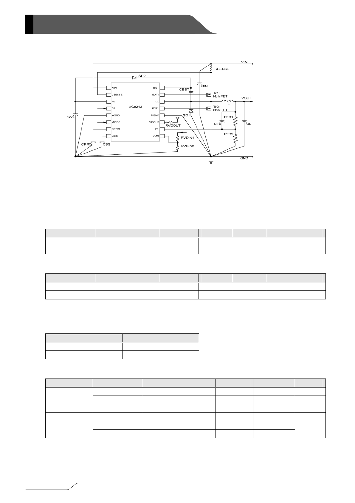
■TYPICAL APPLICATION CIRCUIT
SD2
FB1, 2). Synchronous rectification PWM control can be switched to non-synchronous
SENSE pins) by using the MODE pin.
■FEATURES
Input Voltage Range : 4.0V ~ 25.0V
Output Voltage Range : 1.5V ~ 15.0V externally set
Reference voltage : 1.0V (±2%)
Oscillation Frequency : 300kHz (±15%)
Output Current : 5A (VIN=5.0V, VOUT=3.3V)
Control : PWM/PFM manual control
Current Limit Protection : Sense Voltage=170mV
High Efficiency : 93% (VIN=5.0V,VOUT=3.3V, IOUT=1A]
Detect Voltage Function : Detects 0.9V/Open-drain output
Stand-by Current : ISTB = 4.0μA (MAX.)
Load Capacitor
Shutdown Time
Built-in Bootsrap
Package : TSSOP-16
Environmentally friendly : EU RoHS Compliant, Pb Free
■TYPICAL PERFORMANCE
CHARACTERISTICS
☆GreenOperation Compatible
: Low ESR capacitor
: Adjustable by CPRO pin
: External Nch-Nch Drivers
VIN
CIN
CVL
VDIN
VDOUT
CSS
VIN VSENSE
VDIN
VDOUT
VL
CSS
CPRO
AGND
CPRO
RSENSE
XC9213
BST
EXT1
LX
FB
EXT2
PGND
CEMODE
CBST
Tr1
L
SD1
CFB
Tr2
VOUT
RFB1
CL
RFB2
1/34

XC9213 Series
■PIN CONFIGURATION
■PIN ASSIGNMENT
PIN NUMBER PIN NAME FUNCTION
1
2
3
4
5
6
V
IN
SENSE
V
V
CE
AGND
MODE
7 CPRO
8
9
10
11
12
13
14
15
16
■CE PIN & MODE PIN FUNCTION
CSS
VDIN
FB
VDOUT
PGND
EXT2
LX
EXT1
BST
CE PIN OPERATIONAL STATE
H
L Shut down
Input Voltage
Current Detection
Local Power Supply
L
Chip Enable
Analog Ground
PWM / Current Limit PFM Switch
Protection Time Setting Capacitor Connection
<Set shutdown time of VOUT when detecting overcurrent>
Soft-start Capacitor Connection <Set soft-start time>
Voltage Detector Input (0.9V)
Output Voltage Setting Resistor Connection < Set output voltage freely by split resistors >
Voltage Detector Output (Open-Drain)
Power Ground
Low Side N-ch Driver Transistor <Connect to Gate of Low Side N-ch MOSFET >
Coil Connection
High Side N-ch Driver Transistor <Connect to Gate of High Side N-ch MOSFET >
Bootstrap
Operation
MODE PIN OPERATIONAL STATE
H
L
■PRODUCT CLASSIFICATION
●Ordering Information
XC9213B①②③④⑤-⑥
PWM / Current Limit PFM Automatic Switching Control
(*1)
Synchronous
PWM Control
Non-Synchronous
DESIGNATOR DESCRIPTION SYMBOL DESCRIPTION
①②
③
④⑤-⑥
(*1)
The “-G” suffix indicates that the products are Halogen and Antimony free as well as being fully RoHS compliant.
Reference Voltage 10 1.0V (Fixed)
Oscillation Frequency 3
Package
(Oder Unit)
VR
VR-G
TSSOP-16 (TOP VIEW)
300kHz
TSSOP-16 (3,000/Reel)
TSSOP-16 (3,000/Reel)
2/34

■ABSOLUTE MAXIMUM RATINGS
PAR AMETER SYMBOL RATINGS UNITS
VIN Pin Voltage VIN - 0.3 ~ 30.0 V
VSENSE Pin Voltage VSENSE - 0.3 ~ 30.0 V
VL Pin Voltage VL - 0.3 ~ 6.0 V
CE Pin Voltage (*) CE - 0.3 ~ 30.0 V
MODE Pin Voltage (*) MODE - 0.3 ~ 30.0 V
CPRO Pin Voltage CPRO - 0.3 ~ 6.0 V
CSS Pin Voltage CSS - 0.3 ~ 6.0 V
VDIN Pin Voltage VDIN - 0.3 ~ 6.0 V
FB Pin Voltage FB - 0.3 ~ 6.0 V
VDOUT Pin Voltage VDOUT - 0.3 ~ 30.0 V
EXT2 Pin Voltage EXT2 - 0.3 ~ 6.0 V
Lx Pin Voltage Lx - 0.3 ~ 30.0 V
EXT1 Pin Voltage EXT1 - 0.3 ~ 30.0 V
BST Pin Voltage BST - 0.3 ~ 30.0 V
EXT1 Pin Current IEXT1
EXT2 Pin Current IEXT2
Lx Pin Current ILx 100 mA
Power Dissipation Pd 350 mW
Operational Temperature Range Topr - 40 ~ + 85
Storage Temperature Range Tstg - 55 ~ + 125
(*) CE, MODE pin voltage
1) 1.4V≦High Level≦6V
The CE pin and the MODE pin can be connected directly
2) 6V < High Level < 30V
The CE pin and the MODE pin should be connected to
to the high level power supply.
±100
±100
over 1kΩ resistor when connecting
mA
mA
O
C
O
C
XC9213
Series
IC Inside
CE or
MODE
1.4V<High Level<6V 6V< Hig h Le vel<30V
IC Inside
R>1kΩ
CE or
MODE
3/34

XC9213 Series
■ELECTRICAL CHARACTERISTICS
XC9213B103 (FOSC = 300kHz) Ta =2 5OC
PAR AMETER SYMBOL CONDITIONS MIN. TYP. MAX. UNITS CIRCUIT
Input Voltage (*2) VIN 4.0 - 25.0 V -
Output Voltage
Setting Range
FB Control Voltage VFB 0.980 1.000 1.020 V 1
U.V.L.O. Voltage UVLO Voltage which EXT1 pin starts oscillation 1.0 1.5 2.0 V 2
Supply Current 1 IDD1 CE=VIN, FB=0.9V - 550 800 μA 3
Supply Current 2 IDD2 CE=VIN, FB=1.1V - 450 600 μA 3
Stand-by Current ISTB CE=FB=0V - - 4.0 μA 4
Oscillation Frequency FOSC CE=VIN, FB=0.9V 255 300 345 kHz 5
Maximum Duty Ratio 1 MAXDTY1 CE=VIN, FB=0.9V 91 95 - % 5
Maximum Duty Ratio 2 MAXDTY2 CE=VIN, FB=1.1V - 98 - % 5
PFM Duty Ratio PFMDTY
Sense Voltage VSENSE Voltage which EXT1 pin stops oscillation 145 170 200 mV 7
CPRO time TPRO
Soft-Start Time TSS
Short Protection Circuit
Operating Voltage
Efficiency EFFI
CE "H" Voltage VCEH Voltage which EXT1 pin starts oscillation 1.4 - - V 11
CE "L" Voltage VCEL
MODE "H" Voltage VMODEH Voltage which EXT2 pin starts oscillation 1.4 - - V 12
MODE "L" Voltage VMODEL
EXT1 "H"
ON Resistance
EXT1 "L"
ON Resistance
EXT2 "H"
ON Resistance
EXT2 "L"
ON Resistance
Dead Time 1 TDT1
Dead Time 2 TDT2
CE "H" Current ICEH CE=5.0V - - 0.1 μA 17
CE "L" Current ICEL CE=0V -0.1 - - μA 17
MODE "H" Current IMODEH MODE=5.0V - - 0.1 μA 18
MODE "L" Current IMODEL MODE=0V -0.1 - - μA 18
CSS Current ICSS CSS=0V -4.0 -2.0 - μA 19
FB "H" Current IFBH FB=5.0V - - 0.1 μA 20
FB "L" Current IFBL FB=0V -0.1 - - μA 20
V
OUTSET 1.5 - 15.0 V -
With external components,
VOUT=3V, MODE=0V, IOUT=1mA,
No R
SENSE
CPRO=4700pF, V
Time until V
SENSE=0V0.5V,
DOUT inverts H to L
2.5 3.0 3.9 μs 6
2.3 4.7 9.4 ms 8
With external components,
CSS=4700pF, CE=0V3V,
V
SHORT
Time until voltage becomes V
V
IN-VSENSE: 0.3V fixed, FB: SWEEP.
Voltage which V
DOUT inverts H to L
With external components, I
V
OUT=3.0V
OUT x 0.95
OUT=1A,
Voltage which EXT1 pin voltage holding
"L" level
Voltage which EXT2 pin voltage holding
"L" level
R
EXT1H FB=0.9V, EXT1=3.6V - 18 23 Ω 13
R
EXT1L FB=1.1V, EXT1=0.4V - 11 18 Ω 14
R
EXT2H FB=1.1V, EXT1=3.6V - 18 23 Ω 15
R
EXT2L FB=0.9V, EXT2=0.4V - 4 8 Ω 16
With external components,
EXT1: HL, EXT2: LH
With external components,
EXT2: HL, EXT1: LH
4 8 21 ms 9
0.15 0.40 0.72 V 25
- 93 - % 10
- - 0.4 V 11
- - 0.4 V 12
- 100 - ns 10
- 60 - ns 10
4/34

XC9213
■ELECTRICAL CHARACTERISTICS (Continued)
XC9213B103 (Continued)
●Voltage Regulator (*3)
PAR AMETER SYMBOL CONDITIONS MIN. TYP. MAX.
Output Voltage VLOUT FB=1.1V, ILOUT=10mA 3.86 4.00 4.14 V 21
Load Regulation VLOUT
Input Regulation
●Voltage Detector
VLOUT
VIN・VLOUT
FB=1.1V, 1mA≦I
LOUT≦30mA
FB=1.1V, ILOUT=10mA,
VLOUT+1V≦VIN≦25V
- 45 90 mV 21
- 0.05 0.1 %/V 21
PAR AMETER SYMBOL CONDITIONS MIN. TYP. MAX.
Detect Voltage VDF
Release Voltage (*4) VDR
FB=1.1V,
Voltage which V
FB=1.1V,
Voltage which V
DOUT inverters H to L
DOUT inverters L to H
0.855 0.900 0.925 V 22
0.915 0.954 0.980 V 22
Hysteresis Range HYS FB=1.1V 2.9 6.0 7.5 % 22
Output Current VDIOUT FB=1.1V, VDIN=VDF-0.4V, VDOUT=0.5V
Delay Time TDLY
DR→VDOUT inversion
V
VDIN Current IVDIN VDIN=5.0V
NOTE:
*1: Unless otherwise stated, V
*2: The operation may not be stable at no load, if the step-down ratio (V
*3: The regulator block is used only for bootstrap. Please do not use as a local power supply.
*4: Release voltage: (VDR) = VDF + HYS x VDF
IN=5.0V, CE=5.0V, MODE=5.0V, FB=0.9V
OUT/VIN x 100) becomes lower than 12%.
5 15 20 mA 23
- - 10 μs 22
- - 0.1 μA 24
UNITS
UNITS
Series
CIRCUIT
CIRCUIT
5/34

XC9213 Series
■TEST CIRCUITS
Circuit 1 Circuit 2
OCS
OCS
Circuit 3 Circuit 4
Circuit 5 Circuit 6
VIN
VSE NSE
VL
10uF 1uF
+
-
+-+
-
Circuit 7
CE
AGND
MODE
CPRO
CSS
100p F
BST
EXT1
EXT2
PGND
VDOUT
VDIN
OCS
OCS
LX
OCS
OCS
FB
100k
100k
+
-
Tr1: 2SK2857 (NEC)
+
-
10uF 1uF
VIN
+
VSENSE
VL
CE
AGND
+-+
-
100pF
MODE
CPRO
CSS VDIN
100pF
BST
EXT1
EXT2
PGND
VDOUT
OSC
OSC
100k
100k
LX
SBD1: CRS02 (TOSHIBA)
L: 22μH CDRH6D28 (SUMIDA)
CL: 100μF (OS-CON, NIPPON CHEMI-CON)
C
Tr2: 2SK2857 (NEC)
FB
+
-
IN1: 22μF (OS-CON, SANYO)
RFB1: 220kΩ
R
FB2: 110kΩ
C
FB: 68pF
SBD1
VIN
VSENSE
VL
CE
1uF
+
+
-
+
-
100pF
AGND
MODE
CPRO
CSS
VDOUT
BST
EXT1
EXT2
PGND
VDIN
OSC
OSC
CIN
1uF
Tr1
LX
FB
L
Tr2
RFB1
CFB
CL
RFB2
6/34

■TEST CIRCUITS (Continued)
Circuit 8 Circuit 9
VIN
+
VSENSE
VL
1uF10uF
+
-
+-+
-
4700pF
CE
AGND
MODE
CPR
CSS
100pF
BST
EXT1
EXT2
PGND
VDOUT
VDIN
OSC
OSC
LX
FB
100k 100k
+
-
ceramic
1uF
XB01SB04A2BR (TOREX)
VIN
VSE NSE
VL
CE
AGND
MODE
CPRO
CSS
ceramic
4700pF
BST
EXT1
EXT2
PGND
VDOUT
VDIN
XC9213
Series
VIN
RSENSE: 33 m
ceramic
10uF+10uF
ceramic
1uF
LX
CMS02
(TOSHI BA)
VIN
100k
FB
100k
VL
IRF7313
ceramic
47pF
200k
100k
(IR)
7.4uH(SUMIDA)
25PS100JM12 100uF
GND
VOUT
(NIPPON CHE MI-CON)
Circuit 10 Circuit 11
VIN
XB01SB04A2BR(TOREX)
VIN
VSENSE
VL
ceramic
1uF
ceramic
4700pF
Circuit 12 Circuit 13
+
-
CE
AGND
MODE
CPRO
CSS
ceramic
4700pF
1uF10uF
+
-
100pF
BST
ceramic
EXT1
EXT2
PGND
VDOUT
VDIN
VIN
VSENSE
VL
CE
AGND
MODE
CPRO
CSS V DIN
1uF
LX
CMS02
(TOSHIBA)
100k
FB
100k
VIN
VL
BST
EXT1
LX
EXT2
PGND
VDOUT
FB
ceramic
10uF+10uF
RSENSE: 33 m
IRF7313
(IR)
7.4uH(SUMIDA )
ceramic
47pF
200k
100k
100k 100k
OSC
O
SC
+
-
+
-
25PS 100 JM12 100u F
(NIPPO N CHEMI-CO N)
GND
+
-
VIN
VSE NSE
VL
CE
1uF10u F
+
-
100pF
1uF10uF
+
-
AGND
MODE
CPRO
CSS VDIN
VIN
VSENSE
VL
CE
AGND
MODE
CPRO
CSS VDIN
100pF
BST
EXT1
EXT2
PGND
VDOUT
EXT1
EXT2
PGND
VDOUT
BST
LX
FB
LX
FB
OSC
OSC
100k 100k
+
-
OSC
OSC
50k
+
+
-
-
10uF
7/34

XC9213 Series
■TEST CIRCUITS (Continued)
Circuit 14 Circuit 15
BST
EXT1
EXT2
PGND
VDOUT
VDIN
LX
FB
EXT1
EXT2
PGND
VDOUT
VDIN
BST
LX
+
FB
+
-
V
+
-
V
-
+
-
VIN
VSENSE
VL
1uF10uF
+
-
+
-
Circuit 16 Circuit 17
1uF10uF
+
-
+
-
100pF
CE
AGND
MODE
CPRO
CSS
100pF
VIN
VSENSE
VL
CE
AGND
MODE
CPRO
CSS
VIN
VSENSE
VL
CE
1uF10uF
+
-
1uF10uF
A
+
-
100pF
AGND
MODE
CPRO
CSS VDIN
100pF
VIN
VSENSE
VL
CE
AGND
MODE
CPRO
CSS VDIN
BST
EXT1
EXT2
PGND
VDOUT
PGND
VDOUT
LX
FB
EXT1
EXT2
BST
OSC
OSC
50
10uF
+
+
-
-
LX
FB
100k100k
Circuit 18 Circuit 19
VIN
VSENSE
VL
CE
1uF10uF
+
-
A
+
100pF
AGND
MODE
CPRO
CSS
EXT1
EXT2
PGND
VDOUT
VDIN
BST
LX
FB
100k100k
+
-
8/34
VIN
VSENSE
VL
CE
1uF10uF
+-+
-
AGND
MODE
CPRO
CSS VDIN
A
BST
EXT1
EXT2
PGND
VDOUT
LX
FB
100k100k

■TEST CIRCUITS (Continued)
Circuit 20 Circuit 21
XC9213
Series
VIN
VSENSE
VL
1uF10uF
+
-
100pF
Circuit 22 Circuit 23
1uF10uF
+
-
+
-
CE
AGND
MODE
CPRO
CSS VDIN
VIN
VSENSE
VL
CE
AGND
MODE
CPRO
CSS VDIN
100pF
BST
EXT1
EXT2
PGND
VDOUT
LX
FB
BST
EXT1
EXT2
PGND
VDOUT
100k100k
+
-
A
+
-
100k
LX
+
-
FB
V
+
+
-
-
EXT1
EXT2
PGND
VDOUT
VDIN
BST
LX
FB
BST
EXT1
EXT2
PGND
VDOUT
LX
FB
+
-
100k100k
+
-
A
+
+
-
-
VIN
VSENSE
VL
IL
1uF10uF
↓
1uF10uF
V
+-+
-
100pF
+
-
100pF
CE
AGND
MODE
CPRO
CSS VDIN
VIN
VSENSE
VL
CE
AGND
MODE
CPRO
CSS
Circuit 24 Circuit 25
VIN
VSENS E
VL
CE
1uF10uF
+
-
AGND
MODE
CPRO
CSS VDIN
100pF
EXT1
EXT2
PGND
VDOUT
BST
LX
FB
100k
A
+
-
+
-
VIN
+
-
VSENSE
VL
CE
1uF10uF
+-+
-
AGND
MODE
CPRO
CSS VDIN
100pF
BST
EXT1
EXT2
PGND
VDOUT
OSC
OSC
LX
FB
100k100k
+
-
9/34

XC9213 Series
■BLOCK DIAGRAM
■OPERATIONAL EXPLANATION
< Error Amplifier >
The error amplifier is designed to monitor output voltage. The amplifier compares the reference voltage with the feedback
voltage. When a voltage lower than the reference voltage is fed back, the output voltage of the error amplifier increases.
<Ramp Wave Generator>
The Ramp Wave Generator is organized by the circuits generates a saw-tooth waveform based on the oscillator circuit which
sets an oscillation frequency and a signal from the oscillator circuit.
< PWM Comparator >
The PWM Comparator compares outputs from the error amp. and saw-tooth waveform. When the voltage from the error
amp's output voltage is low, the external switch will be set to OFF.
< U.V.L.O. Comparator >
When the V
< Voltage Regulator >
The voltage regulator block generates 4.0V voltage for the bootstrap circuit. The regulator block is also the power supply for
the internal circuit. Please do not use the regulator block as a local power supply.
<Vref with Soft Start>
The reference voltage, Vref (FB pin voltage)=0.9V, is adjusted and fixed by laser trimming. The soft-start circuit protects
against inrush current, when the power is switched on, and also to protect against voltage overshoot. It should be noted,
however, that this circuit does not protect the load capacitor (C
depending upon the input to the error amps, the operation maintains a balance between the two inputs of the error amps and
controls the EXT1 pin's ON time so that it doesn't increase more than is necessary.
<CE Control Logic >
This function controls the operation and shutdown of the IC. When the voltage of the CE pin is 0.4V or less, the mode will
be chip disable, the channel's operations will stop. The EXT1/2 pins will be kept at a low level (the external N-ch MOSFET
will be OFF). When the CE pin is in a state of chip disable, current consumption will be no more than 4.0μA. When the
CE pin's voltage is 1.4V or more, the mode will be chip enable and operations will recommence. With soft-start, 95% of the
set output voltage will be reached within 8mS (C
< Voltage Detector >
The voltage detector of the XC9213 series is FB type. The reference voltage is 0.9V (TYP.) and the detect voltage can be
set by external resistors. The output is N-ch Open Drain type. The detector is switched on / off with DC/DC by the CE pin.
IN pin voltage is lower than 1.5V (TYP.), the circuit sets EXT/2 to "L" and the external transistor is forced OFF.
L) from inrush current. With the Vref voltage limited and
SS: 4700pF (TYP.)) from the moment of chip enable.
10/34

XC9213
■OPERATIONAL EXPLANATION (Continued)
< Protection Circuit Operation (Current Limit, Latch Protection Circuit, and Short Protection Circuit) >
Shown above is a timing chart for protection circuit operations. When the output current changes from normal to an
overcurrent condition, the current-limiting circuit detects the overcurrent condition as a voltage drop occurring, by virtue of the
current-sensing resistor, at the VSENSE pin. Upon detection, the current-limiting circuit limits the peak current passed
through the high-side N-ch MOSFET at every clock pulse (state ①). It is possible to regulate the value of limited current by
varying the resistance value of the current-sensing resistor. A protection circuit (protective latch circuit), which is designed
to stop the clock, functions if the overcurrent condition continues for a predetermined time (state ②). Time delay before the
protective latch circuit functions is adjustable by the capacitance connected to the CPRO pin (typically 4.7 ms if CPRO has
4,700 pF). The protective latch circuit is reset by turning off and on, or by a disable action followed by an enable action
using the CE pin. If, furthermore, the output is short-circuited (state ③) and V
short-circuit protection circuit detects the condition by means of the FB pin and stops the clock with no time delay. The
short-circuit protection circuit is reset by turning off and on or by a disable action followed by an enable action using the CE
pin, as with the protective latch circuit.
< Mode Control Logic >
A timing chart for automatic switching of current-limiting PFM/PWM is shown above. High-level of the MODE pin allows
PWM operations to occur for synchronous rectification (state ①). When the MODE pin shifts to low-level, current-limiting
PFM/PWM automatic switching occurs with synchronous rectification stopped. Consequently, the low-side N-ch MOSFET
is constantly off under this condition. In addition, a comparison is made for the purposes of automatic switching, between
the ON time of the high-side N-ch MOSFET determined by the internal error amp. and the time required for the current
passed at every clock pulse through the high-side N-ch MOSFET to reach a preset amount of current. The longer one is
selected and becomes on duty (state ② or ③). If the time determined by the error amp. is longer than the other, PWM
operation occurs. Current-limiting PFM operation occurs if the time taken by the current passing at every clock pulse to
reach a preset amount of current is longer. Thus the automatic switching mechanism achieves high efficiency under light to
heavy load conditions.
OUT decreases to a value close to 0 V, the
Series
11/34
XC9213 Series
■TYPICAL APPLICATION CIRCUIT
*Please place CIN close to RSENSE as much as possible, so that an impedance does not occur between the elements.
*Please place C
■EXTERNAL COMPONENTS
* Please refer to the DC/DC simulation section of the Torex web site (http//:www.torex.co.jp) for more details.
●Recommended N-ch MOSFETs for Tr1 and Tr2
OUT: Less than 3A
●I
●IOUT: More than 3A
* It is recommended to use MOSFETs with Ciss less than 3000pF.
* For Tr2, MOSFETs with smaller Crss / (Ciss + Crss) are recommended.
●Recommended Coil (L)
* For stable operation, please use a coil with L less than 22μH.
●Recommended Capacitor (CIN, CVL, CBST, CL)
(*1)Please place CIN close to RSENSE as much as possible, so that an impedance does not occur between the elements.
(*2)Operation may become unstable if a ceramic capacitor is used for C
IN, RSENSE, Tr1, Tr2, L, CL, and SD1 as close as possible to each other.
PART NUMBER MANUFACTURER TYPE Ciss (pF) Crss (pF) Crss / (Ciss + Crss)
uPA2751GR NEC Dual 1040 130 0.111
IRF7313
International Rectifier
Dual 650 130 0.167
PART NUMBER MANUFACTURER TYPE Ciss (pF) Crss (pF) Crss / (Ciss + Crss)
SUD30N03 Vishay Single 1170 30 0.049
SUD70N03 Vishay Single 2700 360 0.118
PART NUMBER MANUFACTURER
CDRH127/LD-7R4 SUMIDA
CDRH127-6R1 SUMIDA
COMPONENTS PART NUMBER
CIN (*1)
- - Ceramic
25SC22M SANYO OS
CVL - - Ceramic
CBST - - Ceramic
CL (*2)
A 1μF ceramic capacitor is recommended for CVL.
20SS150M SANYO OS
25PS100JM12 NIPPON CHEMI-CON -
MANUFACTURER
L.
TYPE VALUE PCS
10μF
22μF
1μF
1μF ~ 4.7μF
150μF
100μF
2
1
1
1
1
12/34
XC9213
■EXTERNAL COMPONENTS (Continued)
●Output Voltage Setting (R
Output voltage can be set by adding external split resistors. Output voltage is determined by the following equation,
based on the values of R
(R
FB1 + RFB2
VOUT = RFB1 / RFB2 + 1
The value of C
fzfb= 1 / (2 x
Adjustments are required from 1kHz to 50kHz depending on the application, value of inductance (L), and value of load
capacity (C
≦2MΩ
π
L).
).
FB, speed-up capacitor for phase compensation, should be adjusted by the following equation.
x CFB x RFB1)≒10kHz
VOUT (V)
1.5 150 300 100
1.8 160 200 100
2.5 360 240 47
3.0 220 110 47
3.3 620 270 27
5.0 300 75 47
●Recommended Schottky Diode (SD1, SD2)
SYMBOL PART NUMBER MANUFACTURER
SD1
SD2
* SD1 and SD2 should be of favorable reverse-current characteristics. If, in particular, SD2 has poor reverse-current characteristics,
CBST cannot be fully charged at high temperatures, resulting, in some cases, in failure to drive Tr1.
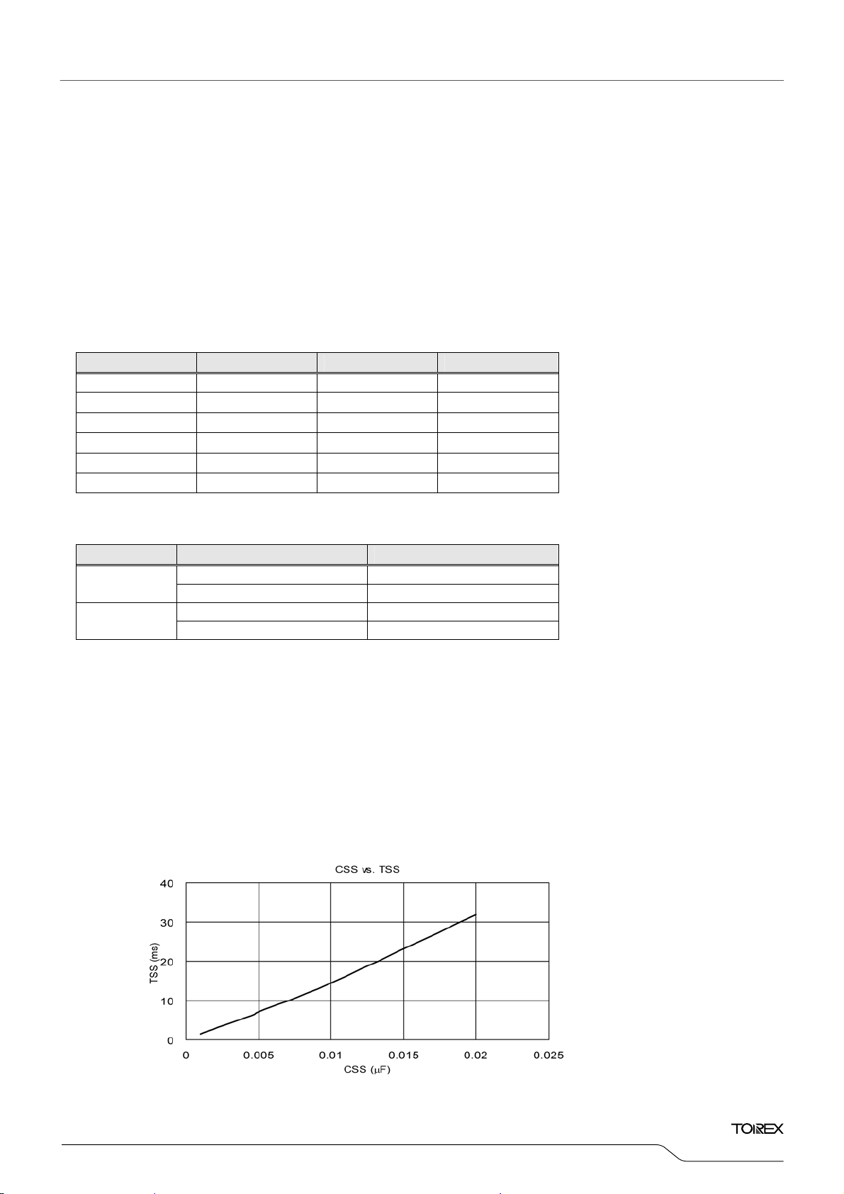
●Setting Latch Protection Circuit Delay Time (CPRO)
Time delay is 4.7 ms (TYP.) under the current conditions if CPRO has 4,700 pF. This time delay is roughly proportional to
the value of CPRO.
ex.) When CPRO is 2200pF, 4.7ms (TYP.) x 2200pF / 4700pF =2.2ms (TYP.)
When CPRO is 0.01μF (10,000pF), 4.7ms (TYP.) x 10000pF / 4700pF =10ms (TYP.)
* For stable operation, please use a capacitor with more than 2200pF as CPRO.
●Setting Soft-Start Time (CSS)
FB1, RFB2, CFB)
FB1 and RFB2. The sum of RFB1 and RFB2 should normally be 2 MΩ or less
RFB1 (Ω) RFB2 (Ω)
CFB (pF)
CMS02 TOSHIBA
DE5PC3 SHINDENGEN
XBS104S14R-G
TOREX
CRS02 TOSHIBA
Relationships between the value of
C
SS and the soft-start time (25
TYP.) are shown at left. For stable
operation, please use a capacitor
with more than 2200pF as C
SS.
Series
O
C
13/34

XC9213 Series
■EXTERNAL COMPONENTS (Continued)
●Sense Resistance (RSENSE)
The below values can be adjusted by using sense resistance (RSENSE).
It is recommended using the R
1) Detect current value of the overcurrent detect circuit
Maximum output current (I
IOUTMAX (A) ≒ 200mV (MAX.) / RSENSE (mΩ)
When 4V≦VIN<5V, the maximum output current becomes larger than the calculated value.
Please also refer to the characteristics performance below.
2) Peak current value of the current limit PFM control
Peak current value of the current limit PFM control (I_PFM) varies depending on the dropout voltage (VDIF), the coil (L)
value and the sense resistance value (R
the characteristic performance below shows the changes in the peak current (I_PFM) when the sense resistance values
(RSENSE) are 20mΩ, 33 mΩ, and 50 mΩ. The peak current varies according to the dropout voltage and the coil value.
3.0
2.5
) (A)
2.0
℃
1.5
1.0
0.5
I_PFM(TYP. 25
0.0
012345
SENSE value in the range of 20mΩ to 100mΩ.
OUTMAX) can be adjusted as the equation below.
SENSE). For the XC9213 series' sample with voltage sense (VSENSE) 170mV,
PFM Pe ak Cu r re n t
RSENSE: 20m
Vdif /L (V /μH)
Ω
PFM Pe ak Cu r re n t
3.0
2.5
) (A)
2.0
℃
1.5
1.0
0.5
I_PFM(TYP. 25
0.0
012345
Vdif/L (V/μH)
RSENSE:33m
Ω
3.0
2.5
) (A)
2.0
℃
1.5
1.0
0.5
I_PFM(TYP. 25
0.0
14/34
PFM Pe ak Cu rr en t
RSENSE: 50m
012345
Vdif/L (V/μH)
Ω
The sense voltage varies within the range of 145 mV≦VSENSE≦200mV.
The peak current as shown in three graphs fluctuates
according to the sample's sense voltage.
■EXTERNAL COMPONENTS (Continued)
●Divided Resistors For VD Input Voltages (RVDIN1, RVDIN2)
Detect voltage of the detector block can be adjusted by the external divided resistors for VD input voltages
(R
VDIN1, RVDIN2) as the equation below.
When 0.855V <
Detect voltage = VDF x (RVDIN1 + RVDIN2) / RVDIN2 [V]
Please select R
●Divided Resistor For VD Output Voltage (R
Output type of the detector block is N-channel open drain. Please use a 1k resistor or more as RVDOUT.
VDF < 0.925V (0.9V TYP.)
VDIN1 and RVDIN2 as the sum of RVDIN1 and RVDIN2 becomes less than 2MΩ.
VDOUT)
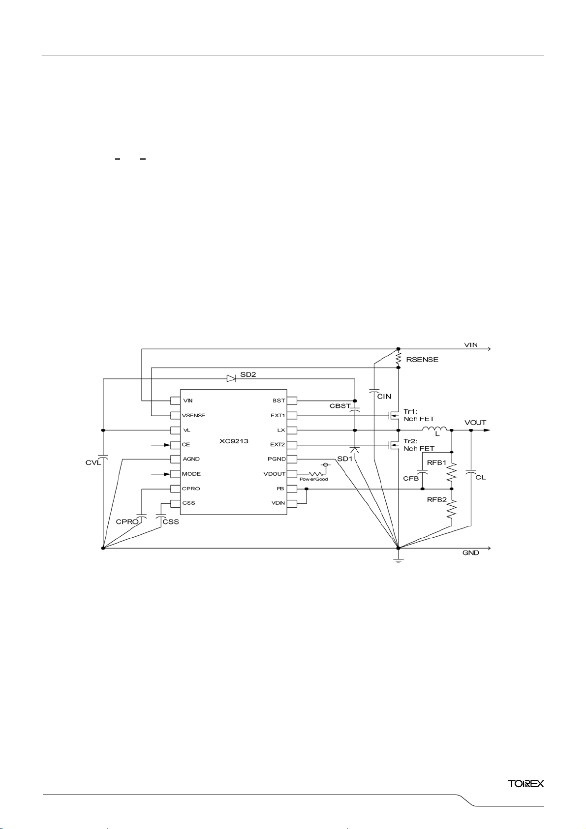
■APPLICATION CIRCUIT EXAMPLE
The application circuit shown below is the example for using the detector block as power good.
Please connect the V
DIN pin with the FB pin as below.
XC9213
Series
15/34
XC9213 Series
■NOTES ON USE
1. Overcurrent Limit Function
The internal current detection circuit is designed to monitor voltage occurs between R
condition. In case that the overcurrent limit function operates when the output is shorted, etc., the current detection circuit
detects that the voltage between R
limit circuit outputs the signal, which makes High side’s N-ch MOSFET turn off. Therefore, delay time will occur (300ns TYP.)
after the current detection circuit detects the SENSE voltage before High side’s N-ch MOSFET turns off. When the
overcurrent limit function operates because of rapid load fluctuation etc., the SENSE voltage will spread during the delay
time without being limited at the voltage value, which is supposed to be limited. Therefore, please be noted to the absolute
maximum ratings of external MOSFET, a coil, and an Schottky diode.
2. Short Protection Circuit
In case that a power supply is applied to the IC while the output is shorted, or the IC is switched to enable state from disable
state via the CE pin, when High side’s N-ch MOSFET is ON and Low side’s N-ch MOSFET is OFF, the potential difference
for input voltage will occur to the both ends of a coil. Therefore, the time rate of coil current becomes large. By contrast, when
High side’s N-ch MOSFET is OFF and Low side’s N-ch MOSFET is ON, there is almost no potential difference at both ends
of the coil since the output voltage is shorted to the Ground. For this, the time rate of coil current becomes quite small. This
operation is repeated within soft-start time; therefore, coil current will increase for every clock. Also with the delay time of the
circuit, coil current will be converged on a certain current value without being limited at the current amount, which is
supposed to be limited. However, step-down operation will stop and the circuit can be latched if FB voltage is decreasing to
the voltage level, which enables to operate a short protection circuit when the soft-start time completes. Even if the FB
voltage is not decreasing to the voltage level, which a short protection circuit cannot be operated, the step-down operation
stops when CPRO time completes, and the circuit will be latched.
Please be noted to the absolute maximum ratings of external MOSFET, a coil, and an Schottky diode.
3. Current Limit PFM Control
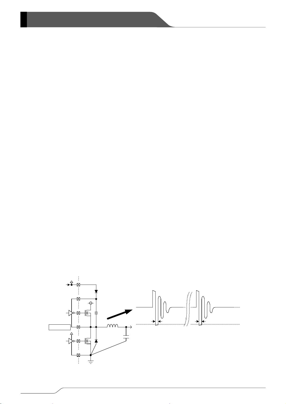
With a built-in bootstrap buffer driver circuit, the XC9213 series generates voltage for Tr1 to be turned on by charging CBST
with VL (4V). When Tr1 is off, Tr2 is on, and the Lx signal is low, it will be suitable timing for charging CBST. (Please refer to
the above figure.) For that reason, at PFM control (MODE: Low), the clock pulses will decrease extremely according to the
decrease of the load current. As a result, it will cause a decrease of charging frequency and an electric discharge of CBST
so that sufficient voltage for the Tr1 to be turned on will not be supplied.
Therefore,
1) Please use a Schottky Barrier Diode with few reverse current values for SD2.
2) Please avoid extreme light loads (e.g. less than a few mA)
Moreover, the above-mentioned operation may occur, influenced by external components including SD2 and ambient
temperature. It’s recommended to use the IC after evaluation with an actual device.
XC9213
SENSE resistors reaches the SENSE voltage (170mV TYP.), and, thereby, the overcurrent
VL(4V)
BST
EXT1
LX
EXT2
PGND
SD2
VIN
Tr1
CBST
L
Tr2
SD1
CL
GND
CBST Charge CBST Charge
LX Waveform (MODE:Low, PFM)
16/34
SENSE resistors in the overcurrent

■NOTES ON USE (Continued)
4. Switching on and off the IC by the input voltage pin
When the IC is switched on and off by the input voltage pin (V
operation because a protection circuit built inside the short-protection circuit, etc. begins to work in order to block ON
signal which is sent before the soft-start capacitor connection pin (C
avoiding this situation;
a) Turn on the power source again after input voltage becomes below U.V.L.O. detect voltage (1.0V MIN.), furthermore,
after the lapse of the time constant of τ=C
SS x 50k.
b) Before turning the power source on again, start-up the IC after resetting the C
Please make sure the C
SS pin is discharged once and the soft-start time is secured when starting up the IC.
IN) instead of the chip enable pin (CE), the IC may stop
SS) resets. The following methods can be used for
SS forcibly and keeping soft-start time.
XC9213
Series
17/34

XC9213 Series
■REFERENCE PCB LAYOUT
●Layout For Using a Dual MOSFET
RVD3
CDD
RVD1
VL
TOREX
XC9213
VER.2.1A
RVD3
CVL
RVD1
VDIN
TOREX
SD2
CSS
IC
CL
CL
+
FB
SD
SD2
CBST
IC
CL
+
RFB2
FB
CVL
CPRO
VOUT
RFB2
CPRO
CSS
RVD2
CIN
SD
CBST
GND
RFB1
CFB
VIN
G
G
TR1
TR2
GND
SD1
CL
CL
RFB1
CFB
VDOUT
CE
MODE
RVD2
VDIN
●Layout For Using a Single MOSFET
<TOP VIEW>
0308
VDOUT
CE
MODE
VL
CDD
<BOTTOM VIEW>
VIN
+
RSENSE
TR
SD
0306
RSENSE
Resistance
SD1
Ceramic Capacitor
Tr
VER.2.0B
L
RSENSE
CIN
RSENSE
XC9213
L
CIN +
Tr
SD
L
+
VOUT
L
Test pin
Resistance
Ceramic Capacitor
Test pin
Tr
* Please use tinned wires etc. for the VIN, the VOUT, and the
GND.
** Please attach test pins etc. to the CE, the MODE, the
EXT, and the EXT2.
*** Please solder mount the R
possible.
SENSE and the CE as close as
18/34

XC9213
Series
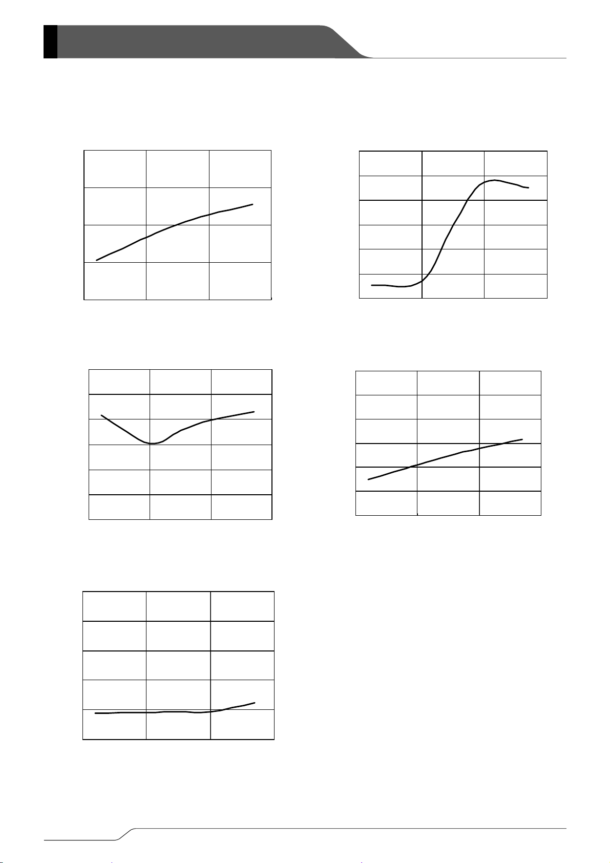
■TYPICAL PERFORMANCE CHARACTERISTICS
(Unless otherwise stated, Topr:25℃)
(1) Output Voltage vs. Output Current <MODE: High>
2.0
V OUT v s . IOUT
FET:IRF7313
2.0
VOUT vs. IOUT
FET:SUD30N03
1.9
1.8
1.7
Output Voltage VOUT (mA)
1.6
1.5
10 100 1000 10000
3.5
3.4
3.3
3.2
VIN:5V, 8V , 15V, 20V
Output Current IOUT (mA)
V OUT v s . IOUT
FET:IRF7313
VIN:5V, 8V , 15V, 20V
1.9
1.8
1.7
Output Voltage VOUT (mA)
1.6
1.5
10 100 1000 10000
3.5
3.4
3.3
3.2
VIN:5V, 8V, 15V, 20V
Output Current IOUT (mA)
VOUT vs. IOUT
FET:SUD30 N03
VIN:5V, 8V, 15V, 20V
Output Voltage VOUT (mA)
3.1
3.0
10 100 1000 10000
5.2
5.1
5.0
4.9
Output Voltage VOUT (mA)
4.8
4.7
10 100 1000 10000
Output Current IOUT (mA)
V OUT v s . IOUT
FET:IRF7313
VIN:8V, 15V, 20V
Output Current IOUT (mA)
Output Voltage VOUT (mA)
3.1
3.0
10 100 1000 10000
5.2
5.1
5.0
4.9
Output Voltage VOUT (mA)
4.8
4.7
10 100 1000 10000
Output Current IOUT (mA)
VOUT vs. IOUT
FET:SUD30 N03
VIN:8V, 15V, 20V
Output Current IOUT (mA)
19/34

XC9213 Series
■TYPICAL PERFORMANCE CHARACTERISTICS (Continued)
(2) Output Voltage vs. Output Current <MODE: Low>
2.0
VOUT vs. IOUT
FET:IRF7313
V OUT v s . IOUT
2.0
FET:SUD30N03
1.9
1.8
1.7
Output Voltage VOUT (mA)
1.6
1.5
10 100 1000 10000
3.5
3.4
3.3
3.2
VIN:5V, 8V , 15V, 20V
Output Current IOUT (mA)
V OUT v s . IOUT
VIN:5V, 8V , 15V, 20V
FET:IRF7313
1.9
1.8
1.7
Output Voltage VOUT (mA)
1.6
1.5
10 100 1000 10000
3.5
3.4
3.3
3.2
VIN:5V, 8V, 15V, 20V
Output Current IOUT (mA)
V OUT v s . IOUT
VIN:5V, 8V, 15V, 20V
FET:SUD30 N03
Output Voltage VOUT (mA)
3.1
3.0
10 100 1000 10000
5.2
5.1
5.0
4.9
Output Voltage VOUT (mA)
4.8
4.7
10 100 1000 10000
Output Current IOUT ( mA)
VOUT vs. IOUT
VIN:8V, 15V, 20V
Output Current IOUT (mA)
FET:IRF7313
Output Voltage VOUT (mA)
3.1
3.0
10 100 1000 10000
5.2
5.1
5.0
4.9
Output Voltage VOUT (mA)
4.8
4.7
10 100 1000 10000
Output Current IOUT (mA)
V OUT v s . IOUT
VIN:8V, 15V, 20V
Output Current IOUT (mA)
FET:SUD30N03
20/34

)
)
)
)
)
)
■TYPICAL PERFORMANCE CHARACTERISTICS (Continued)
(3) Efficiency vs. Output Current <MODE: High>
100
EFFI. vs. IOUT
VOUT:1.8V, FET:IRF7313
100
EFF I. v s . IOU T
V OUT:1 . 8 V , FET: SUD30 N0 3
XC9213
Series
80
60
40
Efficiency EFFI. (%
20
0
10 100 1000 10000
Output Current IOUT (mA)
100
80
60
40
Efficiency EFFI. (%
20
VIN:5V, 8V, 15V, 20V
EFFI vs. IOUT
VOUT:3.3V, FET:IRF7313
VIN:5V, 8V, 15V, 20V
80
60
40
Efficiency EFFI. (%
20
0
10 100 1000 10000
Output Current IOUT (mA)
100
80
60
40
Efficiency EFFI. (%
20
VIN:5V, 8V, 15V, 20V
EFF I. v s . IOU T
VOUT:3.3V, FET:SUD30N03
VIN:5V, 8V , 15V, 20V
0
10 100 1000 10000
100
80
60
40
Efficiency EFFI. (%
20
0
10 100 1000 10000
Output Current IOUT (mA)
EFFI. v s. IOUT
VOUT:5.0V, FET:IRF7313
VIN:8V, 15V, 20V
Output Current IOUT (mA)
0
10 100 1000 10000
100
80
60
40
Efficiency EFFI. (%
20
0
10 100 1000 10000
Output Current IOUT (mA)
EFFI. vs. IOUT
VOUT:5.0V, FET:SUD30N03
VIN:8V, 15V, 20V
Output Current IOUT (mA)
21/34

)
)
)
)
)
)
XC9213 Series
■TYPICAL PERFORMANCE CHARACTERISTICS (Continued)
(4) Efficiency vs. Output Current <MODE: Low>
100
EFFI. vs. IOUT
VOUT:1.8V, FET:IRF7313
100
EFFI. v s. IOUT
V OUT:1 . 8 V , FET: SUD3 0 N03
80
60
40
Efficiency EFFI. (%
20
0
10 100 1000 10000
Output Current IOUT (mA)
100
80
60
40
Efficiency EFFI. (%
20
VIN:5V, 8V, 15V, 20V
EFFI. vs. IOUT
VOUT:3.3V, FET:IRF7313
VIN:5V, 8V, 15V, 20V
80
60
40
Efficiency EFFI. (%
20
0
10 100 1000 10000
100
80
60
40
Efficiency EFFI. (%
20
VIN:5V, 8V, 15V, 20V
Output Current IOUT (mA)
EFFI. vs. IOUT
VOUT:3.3V, FET:SUD30N03
VIN:5V, 8V , 15V, 20V
0
10 100 1000 10000
100
80
60
40
Efficiency EFFI. (%
20
0
10 100 1000 10000
Output Current IOUT (mA)
EFFI. vs. IOUT
VOUT:5.0V, FET:IRF7313
VIN:8V, 15V, 20V
Output Current IOUT (mA)
0
10 100 1000 10000
100
80
60
40
Efficiency EFFI. (%
20
0
10 100 1000 10000
Output Current IOUT (mA)
EFFI. v s. IOUT
V OUT:5 . 0 V , FET: SUD30 N0 3
VIN:8V, 15V, 20V
Output Current IOUT (mA)
22/34

■TYPICAL PERFORMANCE CHARACTERISTICS (Continued)
(5) Ripple Voltage vs. Output Current <MODE: High, Coil: CDRH127/LD-7R4>
80
Vr ipple vs. IOUT
FET:IRF7313, VIN=5V, VOUT=3.3V
80
Vripple vs. IOUT
FET:SUD30N03, VIN=5V, VOUT=3.3V
XC9213
Series
60
CL: 150μF (OS-CON SANYO)
40
CL: 300μF (OS-CON SANYO)
20
Ripple Voltage Vripple (mV)
0
10 100 1000 10000
80
60
40
Output Current IOUT (mA)
Vr ipple vs. IOUT
CL: 150μF ( OS - CON S A NY O)
60
CL: 150μF (OS-CON SANYO)
40
CL: 300μF ( OS - CON S A NY O)
20
Ripple Voltage Vripple (mV)
0
10 100 1000 10000
80
60
40
Output Current IOUT (mA)
Vripple vs. IOUT
FET:SUD30N03, VIN=15V, VOUT=5.0VFET:IRF7313 , VIN=15V , VOUT=5. 0V
CL: 15 0μF (OS-CON SANYO)
20
Ripple Voltage Vripple (mV)
CL: 300μF ( OS - CON S A NY O)
0
10 100 1000 10000
Output Current IOUT (mA)
(6) FB Voltage Temperature Characteristics
VFB vs. Topr
1.04
1.02
1.00
VFB (V)
0.98
FB Voltage VFB (V)
0.96
0.94
-50 0 50 100
Top r (℃)
Temperature Topr(℃)
20
Ripple Voltage Vripple (mV)
0
10 100 1000 10000
VFB Temperature coef f icient vs. Topr
100
-based)
℃
,25
50
℃
0
-50
-100
VFB Temperature c oefficient (ppm/
-50 0 50 100
CL: 300μF ( OS - CON S A NY O)
Output Current IOUT (mA)
(25℃-based)
Topr (℃)
Temperature Topr(℃)
23/34
)
XC9213 Series
■TYPICAL PERFORMANCE CHARACTERISTICS (Continued)
(7) Oscillation Frequency Temperature Characteristics
400
350
)
kHz
(
300
FOSC
250
FOSC vs . Topr
-based)
℃
,25
℃
3000
2000
1000
-1000
-2000
FOSC Temperature Coefficient vs. Topr
-bas ed)
(25
℃
0
200
-50 0 50 100
Temperature Topr(℃)
Topr (
)
℃
(8) Supply Current 1 & 2 Temperature Characteristics
IDD1 v s . Top r
800
700
A)
μ
600
500
400
Supply Current 1 IDD1 (
300
200
-50 0 50 100
Topr (℃)
Temperature Topr(℃)
(9) Stand-by Current Temperature Characteristics
ISTB v s. To p r
10
-3000
-50 0 50 100
FOSC Temperature c oefficient (ppm/
800
700
600
500
400
Supply Current 2 IDD2 (A
300
200
-50 0 50 100
Top r (℃)
Temperature Topr(℃)
IDD2 v s . Topr
Temperature Topr(℃)
Top r (
)
℃
8
A)
μ
6
4
2
Standby Current ISTB (
0
-50 0 50 100
)
Top r (
Temperature Topr(℃)
℃
24/34

)
■TYPICAL PERFORMANCE CHARACTERISTICS (Continued)
(10) VR Output Voltage Temperature Characteristics
4.2
4.1
VLOUT vs. Topr
-bas ed)
℃
,25
℃
VLOUT Temperature coefficient vs. Topr (25℃-bas ed)
100
50
XC9213
Series
4.0
3.9
VD Output Volage VLOUT (V)
3.8
-50 0 50 100
Temperature Topr(℃)
(11)
VD Detect Voltage Temperature Characteristics
V DF v s . Topr
1.00
0.95
0.90
0.85
Detect Voltage VDF (V)
0.80
-50 0 50 100
Temperature Topr(℃)
Top r (
Topr (
)
℃
)
℃
0
-50
-100
-50 0 50 100
VLOUT Temperature c oefficient (ppm/
(12)
1.00
0.95
0.90
0.85
Release Voltage VDR (V)
0.80
Temperature Topr(℃)
Topr (
)
℃
VD Release Voltage Temperature Characteristics
V DR v s. To pr
-50 0 50 100
Temperature Topr(℃)
Top r (
)
℃
(13) CE "H", "L" Voltage Temperature Characteristics
VCEH vs. Topr
1.4
1.2
1.0
0.8
0.6
CE "H" Voltage VCEH (V
0.4
0.2
-50 0 50 100
Temperature Topr(℃)
Top r (
)
℃
1.4
1.2
1.0
0.8
0.6
CE "L" Voltage VCEL (V)
0.4
0.2
-50 0 50 100
VCEL vs. Topr
Temperature Topr(℃)
Topr (
)
℃
25/34

H
XC9213 Series
■TYPICAL PERFORMANCE CHARACTERISTICS (Continued)
(14) MODE "H", "L" Voltage Temperature Characteristics
1.4
VMODEH vs. Topr
1.4
)
1.2
V
(
1.0
1.2
)
V
(
1.0
VMODEL vs. Topr
0.8
0.6
0.4
MODE "H" Voltage VMOD EH
0.2
-50 0 50 100
Temperature Topr(℃)
Topr (℃)
0.8
0.6
0.4
MODE "L" Voltage VMODEL
0.2
-50 0 50 100
Temperature Topr(℃)
Topr (℃)
(15) Sense Voltage Temperature Characteristics (16) Short Protection Circuit Operation Voltage
Temperature Characteristics
VSENSE vs. Topr
0.20
0.18
0.16
0.14
0.12
Sense Voltage VSENSE (V)
VIN:5V, VOUT:1.8V, RSENSE:33mΩ, L:6.1
μ
0.7
0.6
0.5
0.4
0.3
0.2
V SHORT v s . Topr
0.10
-50 0 50 100
Temperature Topr(℃)
Topr (℃)
(17) U.V.L.O. Voltage Temperature Characteristics
UVLO vs. Topr
2.5
2.0
1.5
1.0
U.V.L.O. Voltage UVLO (V)
0.5
-50 0 50 100
Top r (℃)
Temperature Topr(℃)
0.1
Short Prot ect ion Circ uit Operating Volt age VSHOR T (V)
-50 0 50 100
Topr (℃)
Temperature Topr(℃)
26/34
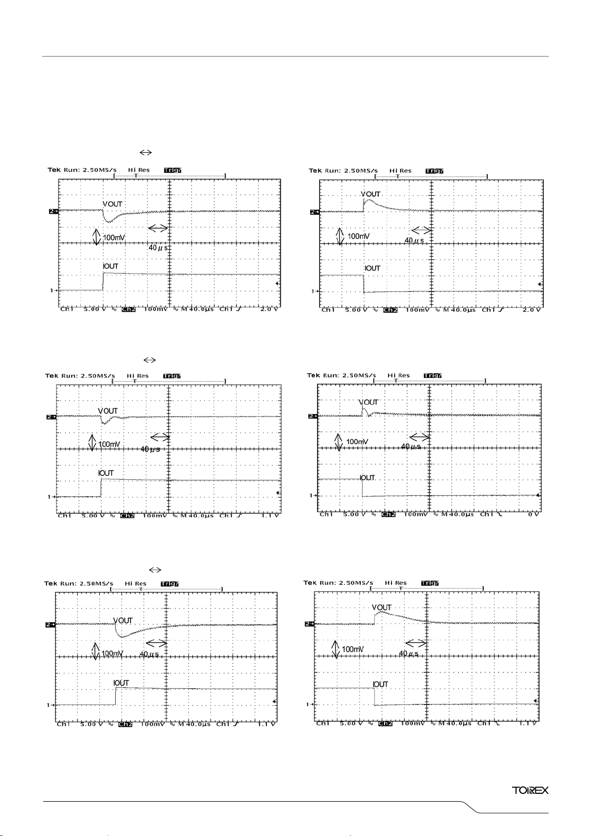
■TYPICAL PERFORMANCE CHARACTERISTICS (Continued)
(18) Load Transient Response Characteristics <MODE: High>
<Condition>
IN: 5V
V
OUT: 1.8V
V
OUT:0A 1A
I
MODE: High
FET:IRF7313 (International Rectifier)
SENSE:33mΩ
R
CL:150μF (OS-CON, SANYO)
L: CDRH127/LD-7R4 (SUMIDA)
XC9213
Series
<Condition>
IN: 15V
V
OUT: 1.8V
V
OUT:0A 1A
I
MODE: High
FET:IRF7313 (International Rectifier)
RSENSE:33mΩ
CL:150μF (OS-CON, SANYO)
L: CDRH127/LD-7R4 (SUMIDA)
<Condition>
V
IN: 5V
OUT: 3.3V
V
OUT:0A 1A
I
MODE: High
FET:IRF7313 (International Rectifier)
SENSE:33mΩ
R
CL:150μF (OS-CON, SANYO)
L: CDRH127/LD-7R4 (SUMIDA)
27/34
XC9213 Series
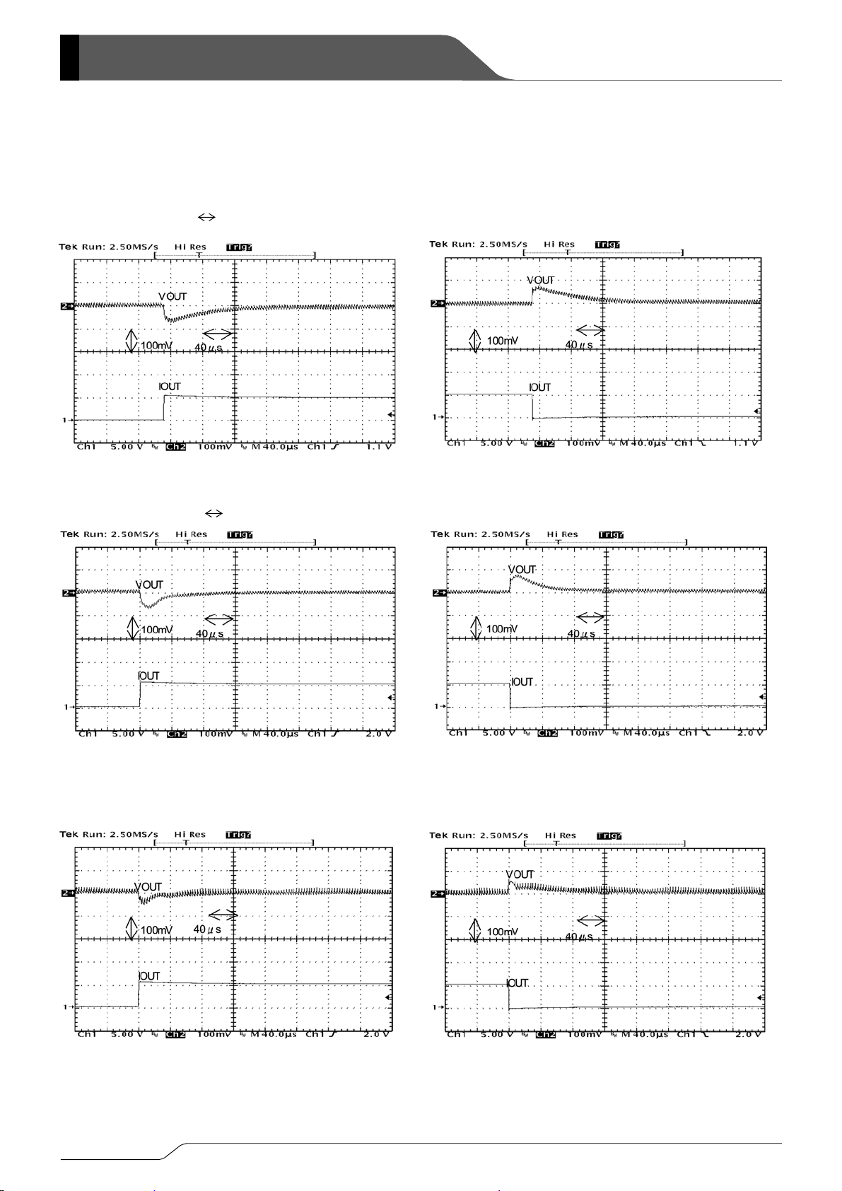
■TYPICAL PERFORMANCE CHARACTERISTICS (Continued)
(18) Load Transient Response Characteristics <MODE: High> (Continued)
<Condition>
IN: 15V
V
OUT: 3.3V
V
OUT:0A 1A
I
MODE: High
FET:IRF7313 (International Rectifier)
SENSE:33mΩ
R
CL:150μF (OS-CON, SANYO)
L: CDRH127/LD-7R4 (SUMIDA)
<Condition>
IN: 5V
V
OUT: 1.8V
V
OUT:0A 1A
I
<Condition>
IN: 15V
V
OUT: 1.8V
V
OUT:0A ⇔1A
I
MODE: High
FET: SUD30N03 (Vishay)
R
SENSE:33mΩ
MODE: High
FET: SUD30N03 (Vishay)
SENSE:33mΩ
R
CL:150μF (OS-CON, SANYO)
L: CDRH127/LD-7R4 (SUMIDA)
CL:150μF (OS-CON, SANYO)
L: CDRH127/LD-7R4 (SUMIDA)
28/34

■TYPICAL PERFORMANCE CHARACTERISTICS (Continued)
(18) Load Transient Response Characteristics <MODE: High> (Continued)
<Condition>
IN: 5V
V
OUT: 3.3V
V
OUT:0A ⇔1A
I
MODE: High
FET:SUD30N03 (Vishay)
SENSE:33mΩ
R
CL:150μF (OS-CON, SANYO)
L:CDRH127/LD-7R4 (SUMIDA)
XC9213
Series
<Condition>
IN: 15V
V
OUT: 3.3V
V
OUT:0A ⇔1A
I
MODE: High
FET: SUD30N03 (Vishay)
SENSE:33mΩ
R
CL:150μF (OS-CON, SANYO)
L: CDRH127/LD-7R4 (SUMIDA)
29/34

XC9213 Series
■TYPICAL PERFORMANCE CHARACTERISTICS (Continued)
(19) Load Transient Response Characteristics <MODE: Low>
<Condition>
IN: 5V
V
OUT: 1.8V
V
OUT:0A ⇔1A
I
MODE: Low
FET:IRF7313 (International Rectifier)
SENSE:33mΩ
R
CL:150μF (OS-CON, SANYO)
L: CDRH127/LD-7R4 (SUMIDA)
<Condition>
IN: 5V
V
OUT: 1.8V
V
OUT:0A ⇔1A
I
MODE: Low
FET: SUD30N03 (Vishay)
SENSE:33mΩ
R
CL:150μF (OS-CON, SANYO)
L: CDRH127/LD-7R4 (SUMIDA)
30/34

p
p
p
■TYPICAL PERFORMANCE CHARACTERISTICS (Continued)
(20) Latch Protection Circuit Operating Waveform <MODE: High>
To
r : - 40℃
<Condition>
IN: 5V
V
OUT: 3.3V
V
MODE: High
FET: SUD30N03 (Vishay)
SENSE:33mΩ
R
CPRO: ceramic 4700pF
CL:150μF (OS-CON, SANYO)
L: CDRH127/LD-7R4 (SUMIDA)
r : 25℃
To
XC9213
Series
To
r : 85℃
31/34

p
p
XC9213 Series
■TYPICAL PERFORMANCE CHARACTERISTICS (Continued)
(21) Short-circuit Protection Circuit Operation Waveform
To
r : - 40℃
<Condition>
IN: 5V
V
OUT: 3.3V
V
MODE: High
FET: SUD30N03 (Vishay)
SENSE:33mΩ
R
CPRO: ceramic 4700pF
CL:150μF (OS-CON, SANYO)
L: CDRH127/LD-7R4 (SUMIDA)
r : 25℃
To
Topr : 85℃
(22) Soft-start Circuit Operation Waveform
<Condition>
V
IN: 5V
OUT: 3.3V
V
OUT:100mA
I
MODE: High
Css: 4700pF
<Condition>
V
IN: 20V
OUT: 15V
V
OUT:100mA
I
MODE: High
Css: 4700pF
32/34
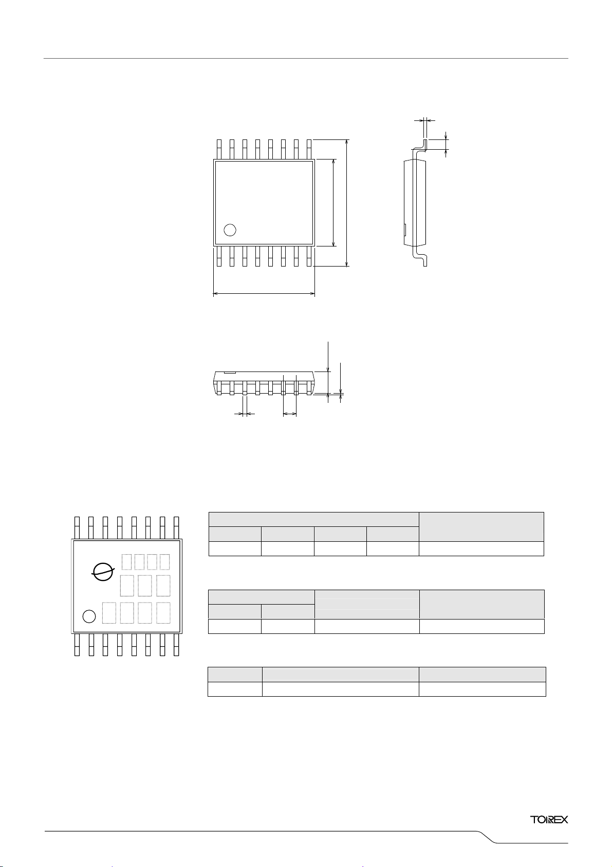
■PACKAGING INFORMATION
●TSSOP-16
■MARKING RULE
●TSSOP-16
14 13 121516
a b c d
① ② ③
⑤ ⑥ ⑦④
34521
TSSOP-16
(TOP VIEW)
91011
876
0. 22
①②③④ represents product series
① ② ③ ④
2 1 3 B
⑤⑥ represents standard voltage
⑤ ⑥
1 0
⑦ represents oscillation frequency
MARK
3
5. 1± 0. 2
+0. 1
-0.05
MARK
6. 4± 0. 2
4. 4± 0. 2
1. 15± 0. 1
0. 1± 0. 05
(0. 65)
MARK
VOLTAGE (V)
1.0
OSCILLATION FREQUENCY
300kHz
+0. 1
0. 22
-0.05
0. 5± 0. 2
PRODUCT SERIES
XC9213B103Vx
PRODUCT SERIES
XC9213B103Vx
PRODUCT SERIES
XC9213B103Vx
XC9213
Series
33/34

XC9213 Series
1. The products and product specifications contained herein are subject to change without
notice to improve performance characteristics. Consult us, or our representatives
before use, to confirm that the information in this datasheet is up to date.
2. We assume no responsibility for any infringement of patents, patent rights, or other
rights arising from the use of any information and circuitry in this datasheet.
3. Please ensure suitable shipping controls (including fail-safe designs and aging
protection) are in force for equipment employing products listed in this datasheet.
4. The products in this datasheet are not developed, designed, or approved for use with
such equipment whose failure of malfunction can be reasonably expected to directly
endanger the life of, or cause significant injury to, the user.
(e.g. Atomic energy; aerospace; transport; combustion and associated safety
equipment thereof.)
5. Please use the products listed in this datasheet within the specified ranges.
Should you wish to use the products under conditions exceeding the specifications,
please consult us or our representatives.
6. We assume no responsibility for damage or loss due to abnormal use.
7. All rights reserved. No part of this datasheet may be copied or reproduced without the
prior permission of TOREX SEMICONDUCTOR LTD.
34/34
 Loading...