

TOREX XC9206, XC9207, XC9208 User Manual
■
■
)
℃
■
XC9206/XC9207/XC9208
Series
ETR0503_002
PWM, PWM / PFM Switchable Step-Down
DC / DC Converters With Driver Transistor Built-In
GENERAL DESCRIPTIO N
The XC9206/XC9207/XC9208 series is a group of DC/DC converters with a built-in 0.4Ω P-channel driver transistor, offered
in a SOT-25 package. The ICs are designed to provide high efficiencies and a stable power supply with an output current of
500mA using only a coil, a diode and two ceramic capacitors connected externally.
Minimum operating voltage of the XC9206/9207 is 1.8V and 2.0V for XC9 208. Output voltage is internally programmable in
a range from 0.9V to 4.0V in 100mV increments (accuracy: ±2.0%). Oscillation frequency i s selectable fro m 300k Hz, 600 kHz
and 1.2MHz so that the frequency best suited to your particular applic ation can be selected. Each series features different
operation modes: PWM control (XC9206 series), automatic PWM/PFM switching control (XC9207 series) and manual
PWM/PFM switching control (XC9208 series). The series gives fast transient response, low ripple and high efficiency over
the full range of load (from light load to high output curre nt conditions). The soft start and current control functions are
internally optimized. During stand-by, all circuits are shutdown to reduce current consumption to as low as 1.0μA or less.
With the built-in U.V.L.O. (Under Voltage Lock Out) function, the internal P-channel driver transistor is forced OFF when input
voltage becomes 1.4V or lower.
■APPLICATIONS
●Mobile phones
(PDC, GSM, CDMA, IMT2000 etc.)
●PDAs, Portable communication modems
●Portable games
●Cameras, digital cameras
●Cordless phones
●Note book computers
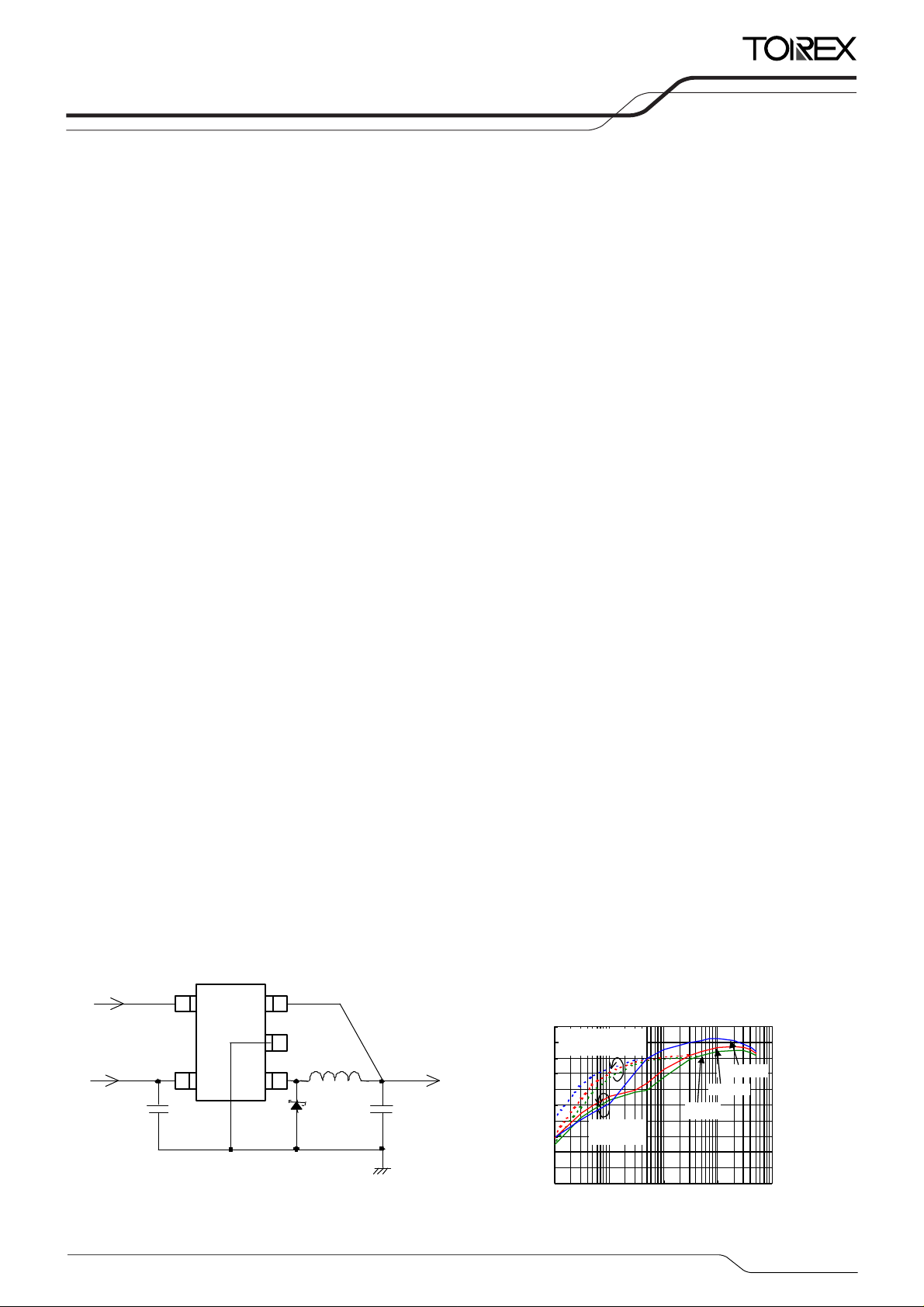
TYPICAL APPLICATION CIRCUIT
CE/MODE
VIN
(ceramic)
L :4.7μF (CDRH 3D16,SUMIDA)
SD :CRS02 (SCHOTTKY DIODE,TOSHIBA)
CL :10μF (ceramic)
C
4
5
IN :4.7μF (ceramic)
CE/
MODE
VIN
VOUT
VSS
3
2
L
Lx
1
SDCIN
VOUT
(500mA)
CL
(ceramic)
FEATURES
P-ch driver Tr. Built-in : ON resistance 0.4Ω
Output Voltage Range : 0.9V ~ 4.0V
(100mV increments)
Oscillation Frequency : 300kHz, 600kHz, 1.2MHz
Fixed oscillation frequency
Accuracy ±15%
Stand-by function : Istb = 1μA (MAX.)
Current Limiter built-in : 600mA
Input Voltage Range : 1.8V ~ 6.0V(XC9206/XC9207)
Output Current : 500mA
Maximum Duty Ratio : 100%
PWM/PFM Switching Control (XC9207 / XC9208)
Ceramic Capacitor Compatible
Soft start circuit built-in
Small Package : SOT-25
■TYPICAL PERFORMANCE
CHARACTERISTICS
●Efficiency vs. Output Current
VOUT=1.8V (Oscillation Frequency 1.2MHz)
100
90
80
70
60
50
40
30
Efficiency EFFI (%
20
10
0
0.1 1 10 100 1000
XC9208A18C
CIN:4.7μF,CL:10μF, L:4.7μH(CDRH3D16),
PWM/PFM
Switchin g Co ntrol
PWM Control
Output Current IOUT (mA)
☆GO-Compatible
Fixed output voltage accuracy ±2%
2.0V ~ 6.0V (XC9208)
SD: C R S02, Topr=25
VIN=2.4V
3.6V
4.2V
1/16
■
■
■
XC9206/XC9207/XC9208
PIN CONFIGURATION
PRODUCT CLASSIFICATION
●Ordering Information
XC9206①②③④⑤⑥: PWM Control
XC9207①②③④⑤⑥: PWM / PFM Automatic Switching Control
XC9208①②③④⑤⑥
DESIGNATOR
①
②③
VIN CE/MODE
Lx V
(TOP VIEW)
Type of DC/DC Converter A
V
SS
SOT-25
OUT
: PWM Control, PWM / PFM Automatic Switching Control Manually Selectable
DESCRIPTION SYMBOL DESCRIPTION
Output Voltage
Series
09~40
09~40 & L
PIN ASSIGNMENT
PIN NUMBER PIN NAME FUNCTION
1 LX Switching Output
2 VSS Ground
3 VOUT Output Voltage Sense
4 CE/MODE Chip Enable/Mode Switch
5 VIN Power Input
: 600mA current limiter, Transistor built-in, output voltage
internally set (V
: 100mV increments
e.g. VOUT=1.5V→②=1, ③=5
: 1.85V V
2.85V VOUT →②=2, ③=L
OUT →②=1, ③=L
OUT product), soft start internally set.
3 : 300kHz
④
⑤ Package M : SOT-25 (SOT-23-5)
⑥
* Output voltage 0.9V ~ 4.0V (100mV increments), 1.85V and 2.85V are standard products.
Output voltage other than these are available as semi-custom products.
Oscillation Frequency
Device Orientation
6 : 600kHz
C : 1.2MHz
R : Embossed tape, standard feed
L : Embossed tape, reverse feed
2/16
■
■
A
XC9206/XC9207/XC9208
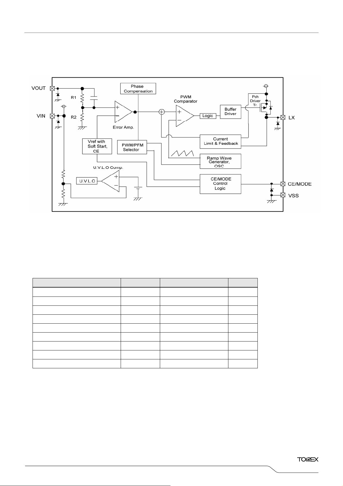
BLOCK DIAGRAM
Note: The signal from CE/MODE Control Logic to PWM/PFM Selector is being fixed to "L" level inside, and XC9206 series chooses
PWM control.
The signal from CE/MODE Control Logic to PWM/PFM Selector is being fixed to "H" level inside, and XC9207 series chooses
only PWM/PFM automatic switching control.
BSOLUTE MAXIMUM RATINGS
Ta=25℃
PARAMETER SYMBOL RATINGS UNITS
VIN Pin Voltage VIN - 0.3 ~ + 6.5 V
VSS Pin Voltage VSS - 0.3 ~ + 6.5 V
Lx Pin Voltage VLx - 0.3 ~ VIN + 0.3 V
VOUT Pin Voltage VOUT - 0.3 ~ + 6.5 V
CE / MODE Pin Voltage VCE - 0.3 ~ VIN + 0.3 V
Lx Pin Current ILx ± 1000 mA
Power Dissipation Pd 250 mW
Operating Temperature Range Topr - 40 ~ + 85
Storage Temperature Range Tstg - 55 ~ + 125
℃
℃
Series
3/16
■
℃
XC9206/XC9207/XC9208
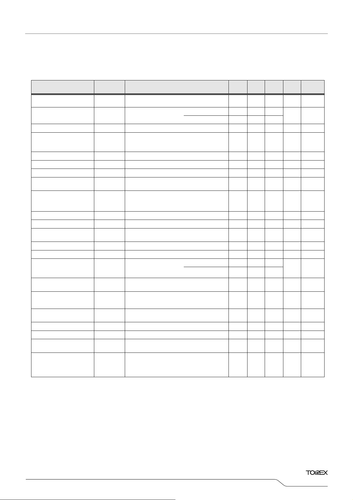
ELECTRICAL CHARACTERISTICS
XC9206A18CMR, XC9207A18CMR, XC9208A18CMR
PARAMETER SYMBOL CONDITIONS MIN. TYP. MAX. UNIT
Output Voltage VOUT
Operating Voltage Range VIN
When connected to ext. components
IN, IOUT=30mA
CE=V
Series
(XC9206, 9207)
(XC9208)
VOUT=1.8V, FOSC=1.2MHz, Ta=25
CIRCUIT
1.764 1.800 1.836 V
1.8 - 6.0
2.0 - 6.0
V
①
①
Maximum Output Current IOUTMAX When connected to ext. components 500 - - mA
CE=V
IN, VOUT=0V,
U.V.L.O. Voltage VUVLO
Supply Current 1 IDD1
Supply Current 2 IDD2 CE=VIN, VOUT=fixed voltage x 1.1V - 98 158
Stand-by Current ISTB CE=VSS, VOUT=fixed voltage x 1.1V - 0 1
Oscillation Frequency FOSC
Voltage which Lx pin voltage holding "L"
(*1)
level
CE=V
IN, VOUT=fixed voltage x 0.9V
When connected to ext. components
IN, IOUT=30mA
CE=V
1.00 1.40 1.78 V
- 255 413
μA ③
μA ③
μA ③
1.020 1.200 1.380 MHz
①
②
①
When connected to ext. components
PFM Pulse Width Rate PFMDTY
(XC9207, XC9208 only), CE=V
OUT=1mA
I
Maximum Duty Cycle MAXDTY CE=VIN, VOUT=0V 100 - %
Minimum Duty Cycle MINDTY CE=VOUT=VIN - - 0 %
Efficiency
(*2)
EFFI
When connected to ext. components,
CE=V
IN, IOUT=100mA
Lx SW ON Resistance RLx CE=VIN, VOUT=0V, ILx=400mA
Current Limit ILIM VIN=CE=5.0V, VOUT=0V - 600 - mA
OUT=0V, When CE
V
CE "H" Voltage VCEH
voltage is applied Lx
determine "H"
V
CE "L" Voltage VCEL
OUT=0V, When CE voltage is applied Lx
determine "L"
IN,
24 30 36 %
- 86 %
(*3)
- 0.4 0.9
(XC9206, 9207)
1.2 - V
(XC9208) 0.9 - V
SS - 0.3 V
V
IN
IN
①
②
②
①
Ω ④
④
V
⑤
⑤
PWM "H" Voltage VPWMH
PWM "L" Voltage VPWML
CE "H" Current ICEH CE=VIN=5.5V, VOUT=0V -0.1 - 0.1
CE "L" Current ICEL CE=0V, VIN=5.5V, VOUT=0V -0.1 - 0.1
Soft-Start Time TSS
When connected to ext. components
(XC9208 only), I
OUT=1mA
When connected to ext. components
(XC9208 only), I
OUT=1mA
(*4)
(*4)
When connected to ext. components
CE=0V → V
IN, IOUT=1mA
IN-0.3 - - V
V
- - V
IN-1.0 V
μA ⑤
μA ⑤
0.8 - 6.0 ms
When connected to ext. components
Latch Time Tlat
Test condition: Unless otherwise stated, VIN = 3.6V
NOTE:
*1: Including hysteresis operating voltage range.
*2: EFFI = [ (output voltage x output current) / (input voltage x input current) ] x 100
*3: On resistance = V
*4: The CE/MODE pin of the XC9208A series works also as an external PWM control and PWM/PFM control switching pin. When the
IC is in the operation, control is switched to the PWM mode when the CE/MODE pin voltage is equal to or greater than V
V, and to the automatic PWM/PFM switching mode when the CE/MODE pin voltage is equal to or lower than V
equal to or greater than V
*5: Time until it short-circuits V
pulse generating.
Lx (measurement voltage) / 0.4
CEH.
OUT with GND through 1Ωof resistance from a state of operation and is set to VOUT=0V from current limit
VIN=CE=5.0V, short VOUT by 1Ω
resistance
(*5)
- - 12.0 ms
IN minus 1.0 V and
①
①
①
⑥
IN minus 0.3
4/16
℃
■
ELECTRICAL CHARACTERISTICS (Continued)
XC9206A25CMR, XC9207A25CMR, XC9208A25CMR
PARAMETER SYMBOL CONDITIONS MIN. TYP. MAX. UNIT CIRCUIT
XC9206/XC9207/XC9208
Series
VOUT=2.5V, FOSC=1.2MHz, Ta=25
Output Voltage VOUT
Operating Voltage Range VIN
When connected to ext. components
IN, IOUT=30mA
CE=V
(XC9206, 9207) 1.8 - 6.0
(XC9208) 2.0 - 6.0
2.450 2.500 2.550 V ①
V ①
Maximum Output Current IOUTMAX When connected to ext. components 500 - - mA ①
CE=V
U.V.L.O. Voltage VUVLO
IN, VOUT=0V,
Voltage which Lx pin voltage holding "L"
(*1)
level
1.00 1.40 1.78 V ②
Supply Current 1 IDD1 CE=VIN, VOUT=fixed voltage x 0.9V - 255 413 μA ③
Supply Current 2 IDD2 CE=VIN, VOUT=fixed voltage x 1.1V - 98 158 μA ③
Stand-by Current ISTB CE=VSS, VOUT=fixed voltage x 1.1V - 0 1 μA ③
Oscillation Frequency FOSC
When connected to ext. components
CE=VIN, IOUT=30mA
1.020 1.200 1.380 MHz ①
When connected to ext. components
PFM Pulse Width Rate PFMDTY
(XC9207, XC9208 only), CE=VIN,
I
OUT=1mA
24 30 36 % ①
Maximum Duty Cycle MAXDTY CE=VIN, VOUT=0V 100 - % ②
Minimum Duty Cycle MINDTY CE=VOUT=VIN - - 0 % ②
Efficiency
(*2)
EFFI
Lx SW ON Resistance RLx CE=VIN, VOUT=0V, ILx=400mA
When connected to ext. components,
IN, IOUT=100mA
CE=V
(*3)
- 0.4 0.9 Ω ④
- 91 % ①
Current Limit ILIM VIN=CE=5.0V, VOUT=0V - 600 - mA ④
OUT=0V, When CE
CE "H" Voltage VCEH
CE "L" Voltage VCEL
PWM "H" Voltage VPWMH
PWM "L" Voltage VPWML
V
voltage is applied Lx
determine "H"
OUT=0V, When CE voltage is applied Lx
V
determine "L"
When connected to ext. components
(XC9208 only), IOUT=1mA
When connected to ext. components
(XC9208 only), I
OUT=1mA
(XC9206, 9207) 1.2 - VIN
(XC9208) 0.9 - V
V
SS - 0.3 V ⑤
(*4)
(*4)
VIN-0.3 - - V ①
- - V
IN
IN-1.0 V ①
V ⑤
CE "H" Current ICEH CE=VIN=5.5V, VOUT=0V -0.1 - 0.1 μA ⑤
CE "L" Current ICEL CE=0V, VIN=5.5V, VOUT=0V -0.1 - 0.1 μA ⑤
Soft-Start Time TSS
When connected to ext. components
CE=0V →V
IN, IOUT=1mA
0.8 - 6.0 ms ①
When connected to ext. components
Latch Time Tlat
Test condition : Unless otherwise stated, VIN = 3.6V
NOTE:
*1 : Including hysteresis operating voltage range.
*2 : EFFI = [ (output voltage x output current) / (input voltage x input current) ] x 100
*3 : On resistance = V
*4 : The CE/MODE pin of the XC9208A series works also as an external PWM control and PWM/PFM control switching pin. When the
IC is in the operation, control is switched to the PWM mode when the CE/MODE pin voltage is equal to or greater than V
V, and to the automatic PWM/PFM switching mode when the CE/MODE pin voltage is equal to or lower than V
equal to or greater than V
*5 : Time until it short-circuits V
limit pulse generating.
LX (measurement voltage) / 0.4
CEH.
OUT with GND through 1Ω of resistance from a state of operation and is set to VOUT=0V from current
VIN=CE=5.0V, short VOUT by 1Ω
resistance
(*5)
- - 12.0 ms ⑥
IN minus 0.3
IN minus 1.0 V and
5/16
 Loading...