

■
■
)
℃
■
XC9206/XC9207/XC9208
Series
ETR0503_002
PWM, PWM / PFM Switchable Step-Down
DC / DC Converters With Driver Transistor Built-In
GENERAL DESCRIPTIO N
The XC9206/XC9207/XC9208 series is a group of DC/DC converters with a built-in 0.4Ω P-channel driver transistor, offered
in a SOT-25 package. The ICs are designed to provide high efficiencies and a stable power supply with an output current of
500mA using only a coil, a diode and two ceramic capacitors connected externally.
Minimum operating voltage of the XC9206/9207 is 1.8V and 2.0V for XC9 208. Output voltage is internally programmable in
a range from 0.9V to 4.0V in 100mV increments (accuracy: ±2.0%). Oscillation frequency i s selectable fro m 300k Hz, 600 kHz
and 1.2MHz so that the frequency best suited to your particular applic ation can be selected. Each series features different
operation modes: PWM control (XC9206 series), automatic PWM/PFM switching control (XC9207 series) and manual
PWM/PFM switching control (XC9208 series). The series gives fast transient response, low ripple and high efficiency over
the full range of load (from light load to high output curre nt conditions). The soft start and current control functions are
internally optimized. During stand-by, all circuits are shutdown to reduce current consumption to as low as 1.0μA or less.
With the built-in U.V.L.O. (Under Voltage Lock Out) function, the internal P-channel driver transistor is forced OFF when input
voltage becomes 1.4V or lower.
■APPLICATIONS
●Mobile phones
(PDC, GSM, CDMA, IMT2000 etc.)
●PDAs, Portable communication modems
●Portable games
●Cameras, digital cameras
●Cordless phones
●Note book computers
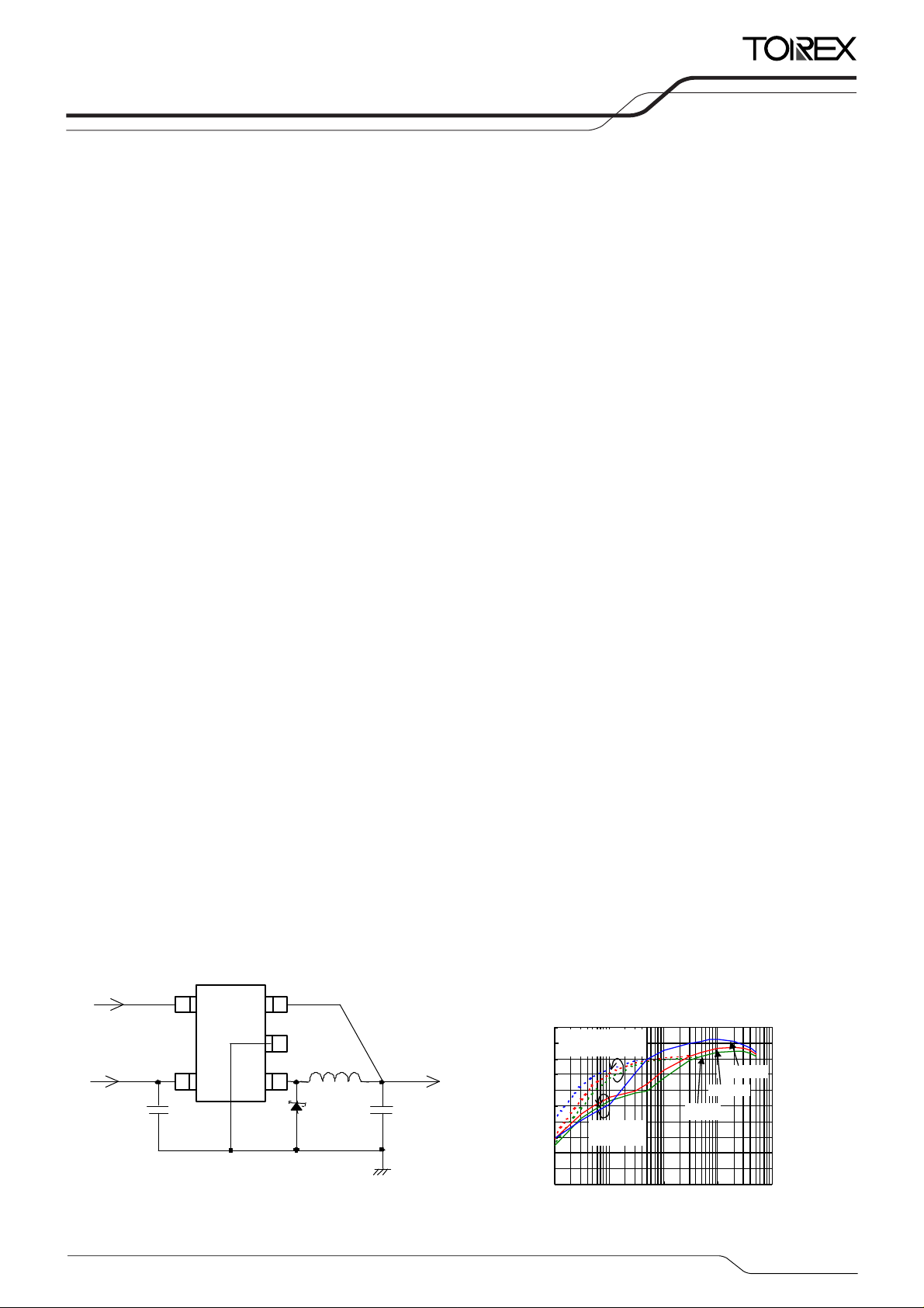
TYPICAL APPLICATION CIRCUIT
CE/MODE
VIN
(ceramic)
L :4.7μF (CDRH 3D16,SUMIDA)
SD :CRS02 (SCHOTTKY DIODE,TOSHIBA)
CL :10μF (ceramic)
C
4
5
IN :4.7μF (ceramic)
CE/
MODE
VIN
VOUT
VSS
3
2
L
Lx
1
SDCIN
VOUT
(500mA)
CL
(ceramic)
FEATURES
P-ch driver Tr. Built-in : ON resistance 0.4Ω
Output Voltage Range : 0.9V ~ 4.0V
(100mV increments)
Oscillation Frequency : 300kHz, 600kHz, 1.2MHz
Fixed oscillation frequency
Accuracy ±15%
Stand-by function : Istb = 1μA (MAX.)
Current Limiter built-in : 600mA
Input Voltage Range : 1.8V ~ 6.0V(XC9206/XC9207)
Output Current : 500mA
Maximum Duty Ratio : 100%
PWM/PFM Switching Control (XC9207 / XC9208)
Ceramic Capacitor Compatible
Soft start circuit built-in
Small Package : SOT-25
■TYPICAL PERFORMANCE
CHARACTERISTICS
●Efficiency vs. Output Current
VOUT=1.8V (Oscillation Frequency 1.2MHz)
100
90
80
70
60
50
40
30
Efficiency EFFI (%
20
10
0
0.1 1 10 100 1000
XC9208A18C
CIN:4.7μF,CL:10μF, L:4.7μH(CDRH3D16),
PWM/PFM
Switchin g Co ntrol
PWM Control
Output Current IOUT (mA)
☆GO-Compatible
Fixed output voltage accuracy ±2%
2.0V ~ 6.0V (XC9208)
SD: C R S02, Topr=25
VIN=2.4V
3.6V
4.2V
1/16
■
■
■
XC9206/XC9207/XC9208
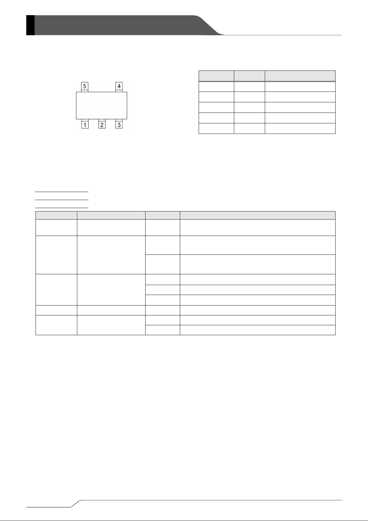
PIN CONFIGURATION
PRODUCT CLASSIFICATION
●Ordering Information
XC9206①②③④⑤⑥: PWM Control
XC9207①②③④⑤⑥: PWM / PFM Automatic Switching Control
XC9208①②③④⑤⑥
DESIGNATOR
①
②③
VIN CE/MODE
Lx V
(TOP VIEW)
Type of DC/DC Converter A
V
SS
SOT-25
OUT
: PWM Control, PWM / PFM Automatic Switching Control Manually Selectable
DESCRIPTION SYMBOL DESCRIPTION
Output Voltage
Series
09~40
09~40 & L
PIN ASSIGNMENT
PIN NUMBER PIN NAME FUNCTION
1 LX Switching Output
2 VSS Ground
3 VOUT Output Voltage Sense
4 CE/MODE Chip Enable/Mode Switch
5 VIN Power Input
: 600mA current limiter, Transistor built-in, output voltage
internally set (V
: 100mV increments
e.g. VOUT=1.5V→②=1, ③=5
: 1.85V V
2.85V VOUT →②=2, ③=L
OUT →②=1, ③=L
OUT product), soft start internally set.
3 : 300kHz
④
⑤ Package M : SOT-25 (SOT-23-5)
⑥
* Output voltage 0.9V ~ 4.0V (100mV increments), 1.85V and 2.85V are standard products.
Output voltage other than these are available as semi-custom products.
Oscillation Frequency
Device Orientation
6 : 600kHz
C : 1.2MHz
R : Embossed tape, standard feed
L : Embossed tape, reverse feed
2/16
■
■
A
XC9206/XC9207/XC9208
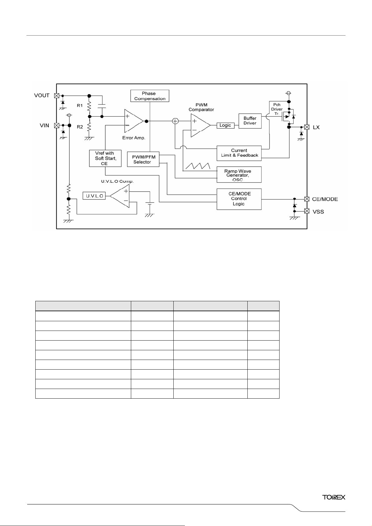
BLOCK DIAGRAM
Note: The signal from CE/MODE Control Logic to PWM/PFM Selector is being fixed to "L" level inside, and XC9206 series chooses
PWM control.
The signal from CE/MODE Control Logic to PWM/PFM Selector is being fixed to "H" level inside, and XC9207 series chooses
only PWM/PFM automatic switching control.
BSOLUTE MAXIMUM RATINGS
Ta=25℃
PARAMETER SYMBOL RATINGS UNITS
VIN Pin Voltage VIN - 0.3 ~ + 6.5 V
VSS Pin Voltage VSS - 0.3 ~ + 6.5 V
Lx Pin Voltage VLx - 0.3 ~ VIN + 0.3 V
VOUT Pin Voltage VOUT - 0.3 ~ + 6.5 V
CE / MODE Pin Voltage VCE - 0.3 ~ VIN + 0.3 V
Lx Pin Current ILx ± 1000 mA
Power Dissipation Pd 250 mW
Operating Temperature Range Topr - 40 ~ + 85
Storage Temperature Range Tstg - 55 ~ + 125
℃
℃
Series
3/16
■
℃
XC9206/XC9207/XC9208
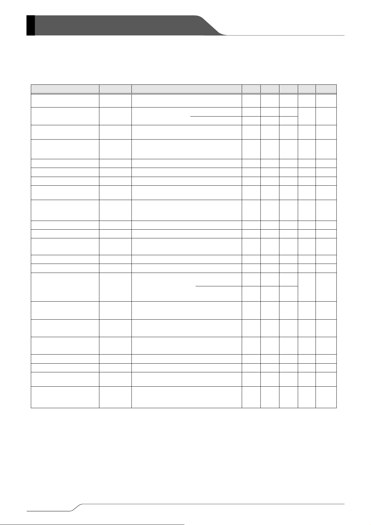
ELECTRICAL CHARACTERISTICS
XC9206A18CMR, XC9207A18CMR, XC9208A18CMR
PARAMETER SYMBOL CONDITIONS MIN. TYP. MAX. UNIT
Output Voltage VOUT
Operating Voltage Range VIN
When connected to ext. components
IN, IOUT=30mA
CE=V
Series
(XC9206, 9207)
(XC9208)
VOUT=1.8V, FOSC=1.2MHz, Ta=25
CIRCUIT
1.764 1.800 1.836 V
1.8 - 6.0
2.0 - 6.0
V
①
①
Maximum Output Current IOUTMAX When connected to ext. components 500 - - mA
CE=V
IN, VOUT=0V,
U.V.L.O. Voltage VUVLO
Supply Current 1 IDD1
Supply Current 2 IDD2 CE=VIN, VOUT=fixed voltage x 1.1V - 98 158
Stand-by Current ISTB CE=VSS, VOUT=fixed voltage x 1.1V - 0 1
Oscillation Frequency FOSC
Voltage which Lx pin voltage holding "L"
(*1)
level
CE=V
IN, VOUT=fixed voltage x 0.9V
When connected to ext. components
IN, IOUT=30mA
CE=V
1.00 1.40 1.78 V
- 255 413
μA ③
μA ③
μA ③
1.020 1.200 1.380 MHz
①
②
①
When connected to ext. components
PFM Pulse Width Rate PFMDTY
(XC9207, XC9208 only), CE=V
OUT=1mA
I
Maximum Duty Cycle MAXDTY CE=VIN, VOUT=0V 100 - %
Minimum Duty Cycle MINDTY CE=VOUT=VIN - - 0 %
Efficiency
(*2)
EFFI
When connected to ext. components,
CE=V
IN, IOUT=100mA
Lx SW ON Resistance RLx CE=VIN, VOUT=0V, ILx=400mA
Current Limit ILIM VIN=CE=5.0V, VOUT=0V - 600 - mA
OUT=0V, When CE
V
CE "H" Voltage VCEH
voltage is applied Lx
determine "H"
V
CE "L" Voltage VCEL
OUT=0V, When CE voltage is applied Lx
determine "L"
IN,
24 30 36 %
- 86 %
(*3)
- 0.4 0.9
(XC9206, 9207)
1.2 - V
(XC9208) 0.9 - V
SS - 0.3 V
V
IN
IN
①
②
②
①
Ω ④
④
V
⑤
⑤
PWM "H" Voltage VPWMH
PWM "L" Voltage VPWML
CE "H" Current ICEH CE=VIN=5.5V, VOUT=0V -0.1 - 0.1
CE "L" Current ICEL CE=0V, VIN=5.5V, VOUT=0V -0.1 - 0.1
Soft-Start Time TSS
When connected to ext. components
(XC9208 only), I
OUT=1mA
When connected to ext. components
(XC9208 only), I
OUT=1mA
(*4)
(*4)
When connected to ext. components
CE=0V → V
IN, IOUT=1mA
IN-0.3 - - V
V
- - V
IN-1.0 V
μA ⑤
μA ⑤
0.8 - 6.0 ms
When connected to ext. components
Latch Time Tlat
Test condition: Unless otherwise stated, VIN = 3.6V
NOTE:
*1: Including hysteresis operating voltage range.
*2: EFFI = [ (output voltage x output current) / (input voltage x input current) ] x 100
*3: On resistance = V
*4: The CE/MODE pin of the XC9208A series works also as an external PWM control and PWM/PFM control switching pin. When the
IC is in the operation, control is switched to the PWM mode when the CE/MODE pin voltage is equal to or greater than V
V, and to the automatic PWM/PFM switching mode when the CE/MODE pin voltage is equal to or lower than V
equal to or greater than V
*5: Time until it short-circuits V
pulse generating.
Lx (measurement voltage) / 0.4
CEH.
OUT with GND through 1Ωof resistance from a state of operation and is set to VOUT=0V from current limit
VIN=CE=5.0V, short VOUT by 1Ω
resistance
(*5)
- - 12.0 ms
IN minus 1.0 V and
①
①
①
⑥
IN minus 0.3
4/16
℃
■
ELECTRICAL CHARACTERISTICS (Continued)
XC9206A25CMR, XC9207A25CMR, XC9208A25CMR
PARAMETER SYMBOL CONDITIONS MIN. TYP. MAX. UNIT CIRCUIT
XC9206/XC9207/XC9208
Series
VOUT=2.5V, FOSC=1.2MHz, Ta=25
Output Voltage VOUT
Operating Voltage Range VIN
When connected to ext. components
IN, IOUT=30mA
CE=V
(XC9206, 9207) 1.8 - 6.0
(XC9208) 2.0 - 6.0
2.450 2.500 2.550 V ①
V ①
Maximum Output Current IOUTMAX When connected to ext. components 500 - - mA ①
CE=V
U.V.L.O. Voltage VUVLO
IN, VOUT=0V,
Voltage which Lx pin voltage holding "L"
(*1)
level
1.00 1.40 1.78 V ②
Supply Current 1 IDD1 CE=VIN, VOUT=fixed voltage x 0.9V - 255 413 μA ③
Supply Current 2 IDD2 CE=VIN, VOUT=fixed voltage x 1.1V - 98 158 μA ③
Stand-by Current ISTB CE=VSS, VOUT=fixed voltage x 1.1V - 0 1 μA ③
Oscillation Frequency FOSC
When connected to ext. components
CE=VIN, IOUT=30mA
1.020 1.200 1.380 MHz ①
When connected to ext. components
PFM Pulse Width Rate PFMDTY
(XC9207, XC9208 only), CE=VIN,
I
OUT=1mA
24 30 36 % ①
Maximum Duty Cycle MAXDTY CE=VIN, VOUT=0V 100 - % ②
Minimum Duty Cycle MINDTY CE=VOUT=VIN - - 0 % ②
Efficiency
(*2)
EFFI
Lx SW ON Resistance RLx CE=VIN, VOUT=0V, ILx=400mA
When connected to ext. components,
IN, IOUT=100mA
CE=V
(*3)
- 0.4 0.9 Ω ④
- 91 % ①
Current Limit ILIM VIN=CE=5.0V, VOUT=0V - 600 - mA ④
OUT=0V, When CE
CE "H" Voltage VCEH
CE "L" Voltage VCEL
PWM "H" Voltage VPWMH
PWM "L" Voltage VPWML
V
voltage is applied Lx
determine "H"
OUT=0V, When CE voltage is applied Lx
V
determine "L"
When connected to ext. components
(XC9208 only), IOUT=1mA
When connected to ext. components
(XC9208 only), I
OUT=1mA
(XC9206, 9207) 1.2 - VIN
(XC9208) 0.9 - V
V
SS - 0.3 V ⑤
(*4)
(*4)
VIN-0.3 - - V ①
- - V
IN
IN-1.0 V ①
V ⑤
CE "H" Current ICEH CE=VIN=5.5V, VOUT=0V -0.1 - 0.1 μA ⑤
CE "L" Current ICEL CE=0V, VIN=5.5V, VOUT=0V -0.1 - 0.1 μA ⑤
Soft-Start Time TSS
When connected to ext. components
CE=0V →V
IN, IOUT=1mA
0.8 - 6.0 ms ①
When connected to ext. components
Latch Time Tlat
Test condition : Unless otherwise stated, VIN = 3.6V
NOTE:
*1 : Including hysteresis operating voltage range.
*2 : EFFI = [ (output voltage x output current) / (input voltage x input current) ] x 100
*3 : On resistance = V
*4 : The CE/MODE pin of the XC9208A series works also as an external PWM control and PWM/PFM control switching pin. When the
IC is in the operation, control is switched to the PWM mode when the CE/MODE pin voltage is equal to or greater than V
V, and to the automatic PWM/PFM switching mode when the CE/MODE pin voltage is equal to or lower than V
equal to or greater than V
*5 : Time until it short-circuits V
limit pulse generating.
LX (measurement voltage) / 0.4
CEH.
OUT with GND through 1Ω of resistance from a state of operation and is set to VOUT=0V from current
VIN=CE=5.0V, short VOUT by 1Ω
resistance
(*5)
- - 12.0 ms ⑥
IN minus 0.3
IN minus 1.0 V and
5/16

℃
■
XC9206/XC9207/XC9208
ELECTRICAL CHARACTERISTICS (Continued)
XC9206A33CMR, XC9207A33CMR, XC9208A33CMR
Series
VOUT=3.3V,FOSC=1.2MHz, Ta=25
PARAMETER SYMBOL CONDITIONS MIN. TYP. MAX. UNIT CIRCUIT
Output Voltage VOUT
Operating Voltage Range VIN
When connected to ext. components
CE=VIN, IOUT=30mA
(XC9206, 9207) 1.8 - 6.0
(XC9208) 2.0 - 6.0
3.234 3.300 3.366 V ①
V ①
Maximum Output Current IOUTMAX When connected to ext. components 500 - - mA ①
CE=V
U.V.L.O. Voltage VUVLO
IN, VOUT=0V,
Voltage which Lx pin voltage holding "L"
(*1)
level
1.00 1.40 1.78 V ②
Supply Current 1 IDD1 CE=VIN, VOUT=fixed voltage x 0.9V - 370 585 μA ③
Supply Current 2 IDD2 CE=VIN, VOUT=fixed voltage x 1.1V - 120 180 μA ③
Stand-by Current Istb CE=VSS, VOUT=fixed voltage x 1.1V - 0 1 μA ③
Oscillation Frequency FOSC
When connected to ext. components
IN, IOUT=30mA
CE=V
1.020 1.200 1.380 MHz ①
When connected to ext. components
PFM Pulse Width Rate PFMDTY
(XC9207, XC9208 only),
IN, IOUT=1mA
CE=V
26 32 38 % ①
Maximum Duty Cycle MAXDTY CE=VIN, VOUT=0V 100 - % ②
Minimum Duty Cycle MINDTY CE=VOUT=VIN - - 0 % ②
Efficiency
(*2)
EFFI
Lx SW ON Resistance RLx CE=VIN, VOUT=0V, ILx=400mA
When connected to ext. components,
IN, IOUT=100mA
CE=V
(*3)
- 0.4 0.9 Ω ④
- 92 % ①
Current Limit ILIM VIN=CE=5.0V, VOUT=0V - 600 - mA ④
CE "H" Voltage VCEH
CE "L" Voltage VCEL
PWM "H" Voltage VPWMH
PWM "L" Voltage VPWML
OUT=0V, When CE
voltage is applied Lx
determine "H"
OUT=0V, When CE voltage is applied
V
Lx determine "L"
When connected to ext. components
(XC9208 only), I
OUT=1mA
When connected to ext. components
(XC9208 only), I
OUT=1mA
(XC9206, 9207) 1.2 - VIN
(XC9208) 0.9 - V
V
SS - 0.3 V ⑤
V
(*4)
(*4)
IN-0.3 - - V ①
- - V
IN
IN-1.0 V ①
V ⑤
V
CE "H" Current ICEH CE=VIN=5.5V, VOUT=0V -0.1 - 0.1 μA ⑤
CE "L" Current ICEL CE=0V, VIN=5.5V, VOUT=0V -0.1 - 0.1 μA ⑤
Soft Start Time TSS
When connected to ext. components
CE=0V → V
IN, IOUT=1mA
0.8 - 6.0 ms ①
When connected to ext. components
Latch Time Tlat
Test condition: Unless otherwise stated, VIN = 5.0V
NOTE:
*1: Including hysteresis operating voltage range.
*2: EFFI = [ (output voltage x output current) / (input voltage x input current) ] x 100
*3: On resistance = V
*4: The CE/MODE pin of the XC9208A series works also as an external PWM control and PWM/PFM control switching pin. When the
IC is in the operation, control is switched to the PWM mode when the CE/MODE pin voltage is equal to or greater than V
V, and to the automatic PWM/PFM switching mode when the CE/MODE pin voltage is equal to or lower than V
equal to or greater than V
*5: Time until it short-circuits V
pulse generating.
LX (measurement voltage) / 0.4
CEH.
OUT with GND through 1Ω of resistance from a state of operation and is set to VOUT=0V from current limit
VIN=CE=5.0V, short VOUT by 1Ω
resistance
(*5)
- - 12.0 ms ⑥
IN minus 1.0 V and
6/16
IN minus 0.3

■
XC9206/XC9207/XC9208
Series
TYPICAL APPLICATION CIRCUIT
CE/MODE
VIN
(ceramic)
* XC9206/9207/9208 series wire connection
■OPERATIONAL EXPLANATION
Each unit of the XC9206/9207/9208 series consists of a reference voltage source, ramp wave circuit, error amplifier, PWM
comparator, phase compensation circuit, output voltage adjustment resistors, driver transistor, current limiter circuit, U.V.L.O.
circuit and others. The series ICs compare, using the error amplifier, the voltage of the internal voltage reference source with
the feedback voltage from the VOUT pin through resistors R1 and R2. Phase compensation is performed on the resulting error
amplifier output, to input a signal to the PWM comparator to determine the turn-on time during PWM operation. The PWM
comparator compares, in terms of voltage level, the signal from the error amplifier with the ramp wave from the ramp wave
circuit, and delivers the resulting output to the buffer driver circuit to cause the Lx pin to output a switching duty cycle. This
process is continuously performed to ensure stable output voltage. T he current feedbac k circuit monito rs the P-channel MOS
driver transistor current for each switching operation, and modulates the error amplifier output signal to provide multiple
feedback signals. This enables a stable fee dback loop even when a low ESR capacitor, such as a ceramic capacitor, is used,
ensuring stable output voltage.
< Reference Voltage Source >
The reference voltage source provides the reference voltage to ensure stable output voltage of the ICs.
< Ramp Wave Circuit >
The ramp wave circuit determines switching frequency. The frequency is fixed internally and can be selected from 300k Hz,
600 kHz and 1.2 MHz. Clock pulses generated in this circuit are used to produce ramp waveforms needed for PWM
operation, and to synchronize all the internal circuits.
< Error Amplifier >
The error amplifier is designed to monitor output voltage. The amplifier compares the reference voltage with the feedback
voltage divided by the internal resistors (R1 and R2). When a voltage lower than the reference voltage is fed back, the outpu t
voltage of the error amplifier increases. The gain and frequency characteristics of the error amplifier output are fixed internally
to deliver an optimized signal to the mixer.
<Current Limit>
The current limiter circuit of the XC9206/9207/9208 series monitors the current flo wing through the P-channel MOS driver
transistor connected to the Lx pin, and features a combination of the constant-current type current limit mode and the operation
suspension mode.
①When the driver current is greater than a specific level, the constant-current type current limit function operates to turn off the
VOUT
CE/
4
MODE
VIN
5
VSS
3
2
Lx
1
L
SDCIN
VOUT
(500mA)
CL
(ceramic)
pulses from the Lx pin at any given timing.
②When the driver transistor is turned off, the limiter circuit is then released from the current limit detection state.
③At the next pulse, the driver transistor is turned on. However, the transistor is immediately turned off in the case of an over
current state.
④When the over current state is eliminated, the IC resumes its normal operation.
The IC waits for the over current state to end by repeating the steps ① through ③ . If an over current state continues for
several msec and the above three steps are repeatedly performed, the IC performs the function of latching the OFF state of the
driver transistor, and goes into operation suspension mode. Once the IC is in suspension mode, operations can be resumed
by either turning the IC off via the CE /MODE pin, or by restoring power to the VIN pin. The suspension mode does not mean a
complete shutdown, but a state in which pulse output is suspended; therefore, the internal circuitry remains in operation. The
constant-current type current limit of the XC9206A/9207A/9208A series can be set at 600 mA.
●FOSC=1.2MHz ●FOSC=600kHz
L : 4.7μH (CDRH3D16, L : 10μH (CDRH4D18C,
SUMIDA) SUMIDA)
SD : CRS02 (TOSHIBA) SD : CRS02 (TOSHIBA)
CIN : 4.7μF (Ceramic) CIN : 4.7μF (Ceramic)
CL : 10μF (Ceramic) CL : 10μF (Ceramic)
●FOSC=300kHz
L : 22μH (CDRH4D18,
SUMIDA)
*SD : Schottky diode
SD : CRS02 (TOSHIBA)
CIN : 4.7μF (Ceramic)
CL : 10μF (Ceramic)
IOUT
VOUT
CE/MODE
Limit < #ms
Limit< #mS Limit> #mS
LX
VIN
Limit > #ms
Cur ren t L im it LEVEL
0mA
VSS
Restart
7/16

■
XC9206/XC9207/XC9208
OPERATIONAL EXPLANATION (Continued)
< U.V .L.O. Circuit>
When the V
output caused by unstable operation of the internal circuitry. W hen the V
operation takes place. By releasing the U.V.L.O. function, the IC performs the soft start function to initiate output startup
operation. The soft start function operates even when the VIN pin voltage falls momentarily below the U.V.L.O. operating
voltage. T he U.V.L.O. circuit does not cause a complete shutdown of the IC, but causes pulse output to be suspended;
therefore, the internal circuitry remains in operation.
< Function of CE/MODE pin >
The XC9206/9207/9208 series will enter into shut down state by inputting a low level signal to the CE/ MODE pin. During a
shut down state, the current consumption of the IC becomes 0μA (TYP.), with a state of high impedanc e at the Lx pin and
V
OUT pin. The IC starts its operation by inputting a high level signal to the CE/MODE pin. The input of the CE/MODE pin is
a CMOS input and the sink current is 0μA (TYP.).
●XC9206A / 07A series - Examples of how to use CE/MODE pin
●XC9208A series - Examples of how to use CE/MODE pin
Intermediate voltage can be generated by RM1 and RM2. Please set the value of each R1, R2, RM1, RM2 at around 100kΩ.
For switches, CPU open-drain I/O port and transistor can be used.
< PWM / PFM >
XC9207/9208 series features PWM/PFM automatic switching control.
With the automatic PWM/PFM switching control function, the series ICs are automatically switched from PWM control to
PFM control mode under light load conditions. If during light load conditions the coil current becomes discontinuous and
on-time rate falls lower than PFM duty, the PFM circuit operates to output a pulse with a fixed on-time rate from the Lx pin.
During PFM operation with this fixed on-time rate, pulses are gener ated at different frequencies according to condition s of
the moment. This causes a reduction in the number of switching operations per unit of time, resulting in efficiency
improvement under light load conditions. However, since pulse output frequency is not constant, consideration should be
given if a noise filter or the like is needed. Necessary conditio ns for switching to PFM operati on depend on inp ut voltage,
load current, coil value and other factors.
IN pin voltage becomes 1.4 V or lower, the P-channel output driver transistor is forced OFF to prevent false pulse
(A) (B)
(A) (B)
Series
IN pin voltage becomes 1.8 V or higher, switching
SW_CE STATUS
ON Chip Disable
A
OFF
ON
B
PWM/PFM automatic switching control (XC9207
PWM/PFM automatic switching control (XC9207)
OFF Chip Disable
SW_CE SW_PMW/PFM STATUS
ON * Synchronous PWM control
OFF ON
A
OFF OFF Chip Disable
ON * Chip Disable
OFF ON
B
OFF OFF Synchronous PWM control
PWM control (XC9206),
PWM control (XC9206),
Non-synchronous PWM/PFM
automatic switching control
Non-synchronous PWM/PFM
automatic switching control
8/16
)
■
y
y
XC9206/XC9207/XC9208
NOTES ON USE
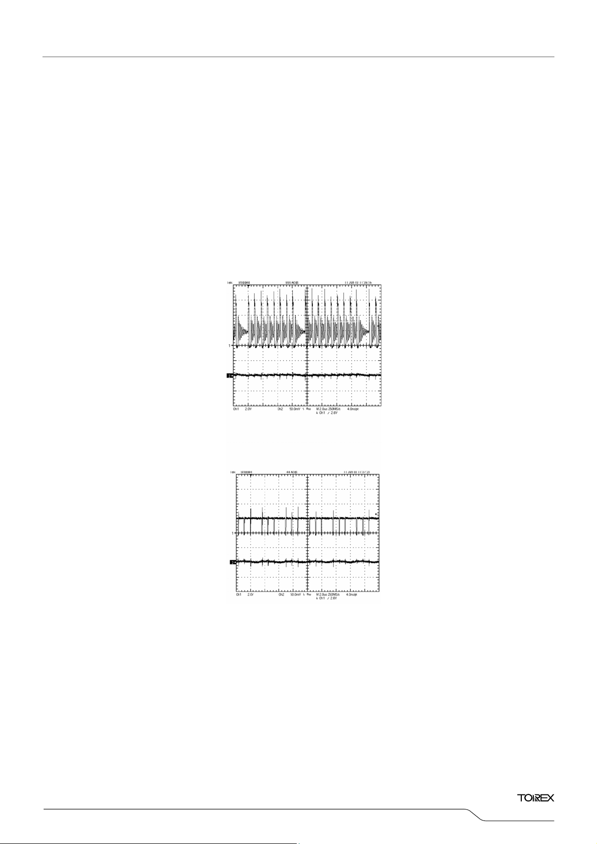
●Application Information
1. The XC9206/9207/9208 series are designed for use with an output ceramic capacitor. If, however, the potential
difference between input and output is too large, a ceramic capacitor may fail to absorb the resulting high switching
energy and oscillation could occur on the output. If the input-output potential difference is large, connect an
electrolytic capacitor in parallel to compensate for insufficient capacitance.
2. Spike noise and ripple voltage arise in a switching regulator as with a DC/DC converter. These are greatly influenced
by external component selection, such as the coil inductance, capacitance values, and board layout of external
components. Once the design has been completed, verific ation with actual components should be done.
3. When the difference between V
and there is the possibility that some cycles may be skipped completely.
●Oscillation Wave Form (FOSC=1.2MHz)
① VIN = 5.5V, VOUT=1.8V, IOUT=10mA
4. When the difference between VIN and VOUT is small, and the load current is heavy, very wide pulses will be outputted
and there is the possibility that some cycles may be skipped completely: in this case, the Lx pin may not go low at all.
●Oscillation Wave Form (FOSC=1.2MHz)
② VIN = 2.0V, VOUT=1.8V, IOUT=60mA
5. With the IC, the peak current of the coil is controlled by the current limit circuit. Since the peak current increases when
dropout voltage or load current is high, current limit starts operating, and this can lead to instability. When peak current
becomes high, please adjust the coil inductance value and fully check the circuit operation. In addition, please
calculate the peak current according to the following formula:
Ipk = (V
IN - VOUT) x On Duty / (2 x L x FOSC) + IOUT
OnDut
: OnDuty ratio of Pch Driver Transistor
L : Coil Inductance Value
FOSC : Oscillation Frequenc
6. When the peak current which exceeds limit current flows within the specified time, the built-in P-ch driver transistor is
turned off. During the time until it detects limit current and before the built-in transistor can be turned off, the current
for limit current flows; therefore, care must be taken when selecting the rating for the coil or the schottky diode.
7. When V
IN is less than 2.4V, limit current may not be reached because voltage falls caused by ON resistance.
IN and VOUT is large and the load current is light, very narrow pulses will be outputted,
CH1 : Lx
L
: 4.7μH
(CDRH3D16,
SUMIDA)
OUT
CH2 : V
AC-COUPLED
CH1 : Lx
SD : CRS02 (TOSHIBA)
CIN
CL
L
: 4.7μF
: 10μF
: 4.7μH
(Ceramic)
(Ceramic)
(CDRH3D16,
SUMIDA)
SD : CRS02 (TOSHIBA)
CH2 : V
OUT
AC-COUPLED
CIN
CL
: 4.7μF
: 10μF
(Ceramic)
(Ceramic)
Series
9/16

■
XC9206/XC9207/XC9208
NOTES ON USE (Continued)
●Application Information (Continued)
8. Care must be taken when laying out the PC Board, in order to prevent misoperation of the current limit mode.
Depending on the state of the PC Board, latch time may become longer and latch operation may n ot work. In order to
avoid the effect of noise, the board should be laid out so that capacitors are placed as close to the chip as possible.
9. Use of the IC at voltages below the recommended voltage range may lead to instability.
10. This IC should be used within the stated absolute maximum ratings in order to prevent damage to the device.
11. Depending on the input-output voltage differential, or load current, some pulses may be skipped, and the ripple voltage
may increase. When the series' duty cycle is digitally s ignalized, the linear duty cycle and the digitally signalized dut y
cycle cannot carry out completely the same change, which means that the duty cycle does not change li nearly. T he
output is stabilized by applying the phase compensation and adjusting the duty cycle, even when the duty cycle loses the
linear change in the whole circuit. When the state where the output was stabilized is continued by applying phase
compensation to duty cycle which lost linearity, ripple voltage does not increase more than it. The ripple voltage may
increase to about several 10mV according to operating conditions. It is possible, by increasing the capacitance values,
to reduce the ripple voltage. The operating conditions are greatly influenced by the dropout voltage, the load current, the
delay-time, or the external components, such as the coil inductance, and the capacitance values. Verification with actual
parts should be done.
●The Increase of Ripple Voltage (1.2MHz)
CH2: V
AC-COUPLED
CH2: V
AC-COUPLED
CH1: Lx
OUT
③ V
CH1: Lx
OUT
① V
IN=4.2V, VOUT=1.8V, IOUT=180mA ② VIN=4.2V, VOUT=1.8V, IOUT=60mA
IN=3.6V, VOUT=1.8V, IOUT=30mA
Series
AC-COUPLED
CH1: Lx
CH2: V
OUT
L
: 4.7μH
(CDRH3D16,
SUMIDA)
SD : CRS02 (TOSHIBA)
CIN
CL
: 4.7μF
: 10μF
(Ceramic)
(Ceramic)
10/16

■
NOTES ON USE (Continued)
●Instructions on Pattern Layout
1. In order to stabilize VDD's voltage level, we recommend that a by-pass capacitor (CIN) be connected as
close as possible to the V
2. Please mount each external component as close to the IC as poss ible, and connect it to GND with the
shortest possible PCB traces.
3. Wire external components as close to the IC as possible and use thick, short connecting traces to reduce
the circuit impedance.
4. Make sure that the PCB GND traces are as thick as possible, as variations in groun d potential caused by
high ground currents at the time of switching may result in instability.
5. Please connect SD anode directly to the by-pass capacitor C
the V
pin of the IC. Also, take distance between the VSS pin and the SD anode for having large impedance
SS
as possible. We recommend that a ferrite bead mount pattern be arranged for the case that the SD noise
can not be reduced by using the pattern layout as shown below.
6. Please do not make the traces under the IC to carry switching main current. It may cause a malfunction of
the IC.
IN & VSS pins.
XC9206/XC9207/XC9208
(-) in order to minimize SD noise affect on to
IN
Series
<TOP VIEW>
VSS
CE
VIN
Ferrite Bead
<BOTTOM VIEW>
VOUT
L
XC9206/07/08
R.1.1 SD
SOT-25
Figure XC9206/07/08Series Pattern Layout
11/16

■
②
/
V
A
V
/
/
V
A
④
⑥
XC9206/XC9207/XC9208
Series
TEST CIRCUITS
Circuit ① Circuit
CIN
CE
VOUT
4
/MODE
5
VSS
3
2
LxVIN
1
L
SD
CL
RL
1μF
VOUT
CE
4
MODE
VI
5
VSS
3
2
Lx
1
200
Ω
Circuit ③ Circuit
CE
/MODE
VOUT
VSS
34
2
Lx
VIN
5
1
1μF
1μF
VOUT
CE
4
MODE
VIN
5
VSS
3
2
Lx
1
L
Circuit ⑤ Circuit
H
CE
VOUT
VSS
34
2
Lx
1
1k
Ω
/MODE
L
VIN
5
1μF
CIN
CE
VOUT
4
MODE
5
VSS
3
2
LxVI
1
L
SD
CL
1
Ω
1.2MHz 600kHz 300kHz
12/16
CIN
CL
4.7μF (ceramic) 4.7μF (ceramic) 4.7μF (ceramic)
10μF (ceramic) 10μF (ceramic) 10μF (ceramic)
L
4.7μH 10μH 22μH
SD Schottky Diode Schottky Diode Schottky Diode

■
TYPICAL PERFORMANCE CHARACTERISTICS
(1) Output Voltage vs. Output Current
VOUT=1.8V (Oscillation Frequency1.2MHz)
CIN:4.7μF,CL:10μF, L: 4. 7μH(CDRH3D16),
2
1.9
(V)
OUT
1.8
1.7
XC9208A18C
PWM/PFM
Switching Control
PWM Control
SD:CRS02, Topr=25
VIN=2.4V
3.6V
4.2V
℃
(V)
OUT
2
1.9
1.8
1.7
1.6
Output Voltage VOUT (V)
Output Voltage: V
1.5
0.1 1 10 100 1000
Output Current: I
Output Current IOUT (mA)
OUT
XC9208A183
VOUT=1.8V (Oscillation Frequency 300kHz)
CIN:4.7μF,CL:10μF, L: 22μH(CDRH4D28C),
2
SD:CRS02, Topr=25
(mA)
(2) Efficiency vs. Output Current
℃
1.6
Output Voltage VOUT (V)
Output Voltage: V
1.5
1.9
(V)
OUT
1.8
1.7
1.6
Output Voltage: V
Output Voltage VOUT (V)
1.5
0.1 1 10 100 1000
PWM/PFM
Switching Control
PWM Control
Output Current: I
Output C urrent IOU T (m A)
3.6V, 4.2V
VIN=2.4V
Efficiency: EFFI (%) Efficiency: EFFI (%)
(mA) Output Current: I
OUT
Efficiency: EFFI (%)
XC9206/XC9207/XC9208
XC9208A186
VOUT=1.8V (Oscillation Frequency 600kHz)
CIN:4.7μF,CL:10μF, L:10μH(CDRH4D18C),
SD:CRS02, Topr=25
Switching Control
PWM
Control
3.6V, 4.2VPWM/PFM
VIN=2.4V
0.1 1 10 100 1000
Output Current: I
Output C urrent IOU T (m A)
Output Current: I
OUT
OUT
OUT
(mA)
(mA)
(mA)
℃
Series
Output Current: I
(mA) Output Current: I
OUT
OUT
(mA)
13/16

■
℃
℃
℃
●SOT
■
r
r
r
XC9206/XC9207/XC9208
Series
TYPICAL PERFORMANCE CHARACTERISTICS (Continued)
(3) Ripple Voltage vs. Output Current
VOUT=1.8V (Oscillation Frequency 1.2MHz)
(mV)
100
80
60
40
PWM/ PFM Sw i tching
20
Ripple Voltage Vr (mV)
Ripple Voltage: V
0
0.1 1 10 100 1000
XC9208A18C
CIN:4.7μF,CL:10μF, L: 4. 7μH(CDRH3D16),
Control
Output Current IOUT (mA)
Output Current: I
SD:CRS02, Topr=25
PWM Control
3.6V
VIN=2.4V
(mA)
OUT
4.2V
VOUT =1.8V (Oscillation Frequency 600kHz)
CIN:4.7μF,CL:10μF, L: 10μH(CDRH4D18C),
100
80
(mV)
60
PWM/ PFM Swit c hing Cont rol
40
20
Ripple Voltage: V
Ripple Voltage Vr (mV)
0
0.1 1 10 100 1000
XC9208A186
Output Current: I
Output Current IOUT (mA)
VOUT=1.8V (Oscillation Frequency 300kHz)
100
XC9208A183
CIN:4.7μF,CL:10μF, L: 22μH(CDRH3D28C),
SD:CRS02, Topr=25
(mV)
Ripple Voltage V r (mV)
Ripple Voltage: V
80
60
40
20
PWM/PFM Swit c hing
Control
VIN=2.4V
PWM Control
3.6V
4.2V
0
0.1 1 10 100 1000
Output Current IOUT (mA)
Output Current: I
OUT
(mA)
PACKAGING INFORMATION
-25
SD:C R S02, Topr=25
PWM Control
4.2V
3.6V
OUT
VIN=2.4V
(mA)
14/16

●SOT
■
XC9206/XC9207/XC9208
MARKING RULE
-25
54
① ② ③ ④
123
SOT-25
(TOP VIEW)
① Represents product name and type of DC/DC converters
MARK PRODUCT SERIES
6 XC9206AxxxMx
7 XC9207AxxxMx
8
* Character inversion is used.
② Represents integer of outp ut voltage and oscill ation frequency
MARK
FOSC=300kHz FOSC=600kHz FOSC=1.2MHz
XC920xx②x3Mx XC920xx②x6Mx XC920xx②xCMx
0 0 A 0.x
1 1 B 1.x
2 2 C 2.x
3 3 D 3.x
4 4 E 4.x
③ Represents decimal number of outpu t voltage and oscillation frequency
MARK
FOSC=300kHz FOSC=600kHz FOSC=1.2MHz
XC920xxx③3Mx XC920xxx③6Mx XC920xxx③CMx
0 A A x. 0
1 B B x. 1
2 C C x. 2
3 D D x. 3
4 E E x. 4
5 F F x. 5
6 H H x. 6
7 K K x. 7
8 L L x. 8
Z Y Y x. 85
9 M M x. 9
* Output voltage 0.9V ~ 4.0V (100mV increments), 1.85V and 2.85V are standard products.
Output voltages other than these are available as semi-custom products.
②③ example :
OSCILLATION
FREQUENCY
VOUT=3.3V VOUT=5.0V VOUT=1.85V
② ③ ② ③ ② ③
MARK
300kHz 3 3 5 0 1 Z
600kHz 3 D 5 A 1 Y
1.2MHz D D F A B Y
④ Represents production lot number
0 to 9, A to Z repeated (G, I, J, O, Q, W excepted)
Series
XC9208AxxxMx
OUTPUT VOLTAGE
(V)
OUTPUT VOLTAGE
(V)
15/16

XC9206/XC9207/XC9208
1. The products and product specifications containe d herein are subject to change without
notice to improve performance characteristics. Consult us, or our representatives
before use, to confirm that the information in this catalog is up to date.
2. We assume no responsibility for any infringement of patents, patent rights, or other
rights arising from the use of any information and circuitry in this catalog.
3. Please ensure suitable shipping controls (including fail-safe designs and aging
protection) are in force for equipment employing products listed in this catalog.
4. The products in this catalog are not developed, designed, or approv ed for use with such
equipment whose failure of malfunction can be reasonably expected to directly
endanger the life of, or cause significant injury to, the user.
Series
(e.g. Atomic energy; aerospace; transport; combustion and associated safety
equipment thereof.)
5. Please use the products listed in this catalog within the specified ranges.
Should you wish to use the products under conditions exceeding the specifications,
please consult us or our representatives.
6. We assume no responsibility for damage or loss due to abnormal use.
7. All rights reserved. No part of this catalog may be copied or reproduced without the
prior permission of Torex Semiconductor Ltd.
16/16
 Loading...