

TOREX XC9135, XC9136 User Manual
XC9135/XC9136 Series
1A Driver Transistor Built-In, Multi Functional Step-Up DC/DC Converters
■GENERAL DESCRIPTION
XC9135/XC9136 series are synchronous step-up DC/DC converters with a 0.2Ω(TYP.) N-channel driver transistor and a 0.2
Ω(TYP.) synchronous P-channel switching transistor built-in. A highly efficient and stable current can be supplied up to 1.0A by
reducing ON resistance of the built-in transistors.
The series are able to start operation under the condition which has 0.9V input voltage to generate 3.3V output voltage with a 33
Ωload resistor, suitable for mobile equipment using only one Alkaline battery or one Nickel metal hydride battery.
During the operation of a shutdown, the load disconnection function enables to cut the current conduction path from the input to
the output.
The output voltage is selectable in 0.1V increments within 1.8~5.0V (±2.0% accuracy).
The UVLO function of the XC9135 series is capable to reduce leaking potassium hydroxide by stopping IC operation while
battery voltage is declining. The release voltages of UVLO are 0.85V (±6.0% accuracy) and 1.6V (±3.0% accuracy), and
selectable voltages range of 0.9V~3.0V.
■APPLICATIONS
●Digital audios
●Digital cameras, Video equipments
●Wireless mice
●Various standard power supplies using batteries
such as alkaline (1 to 3 cells), nickel metal
hydride, or lithium ion (1 cell)
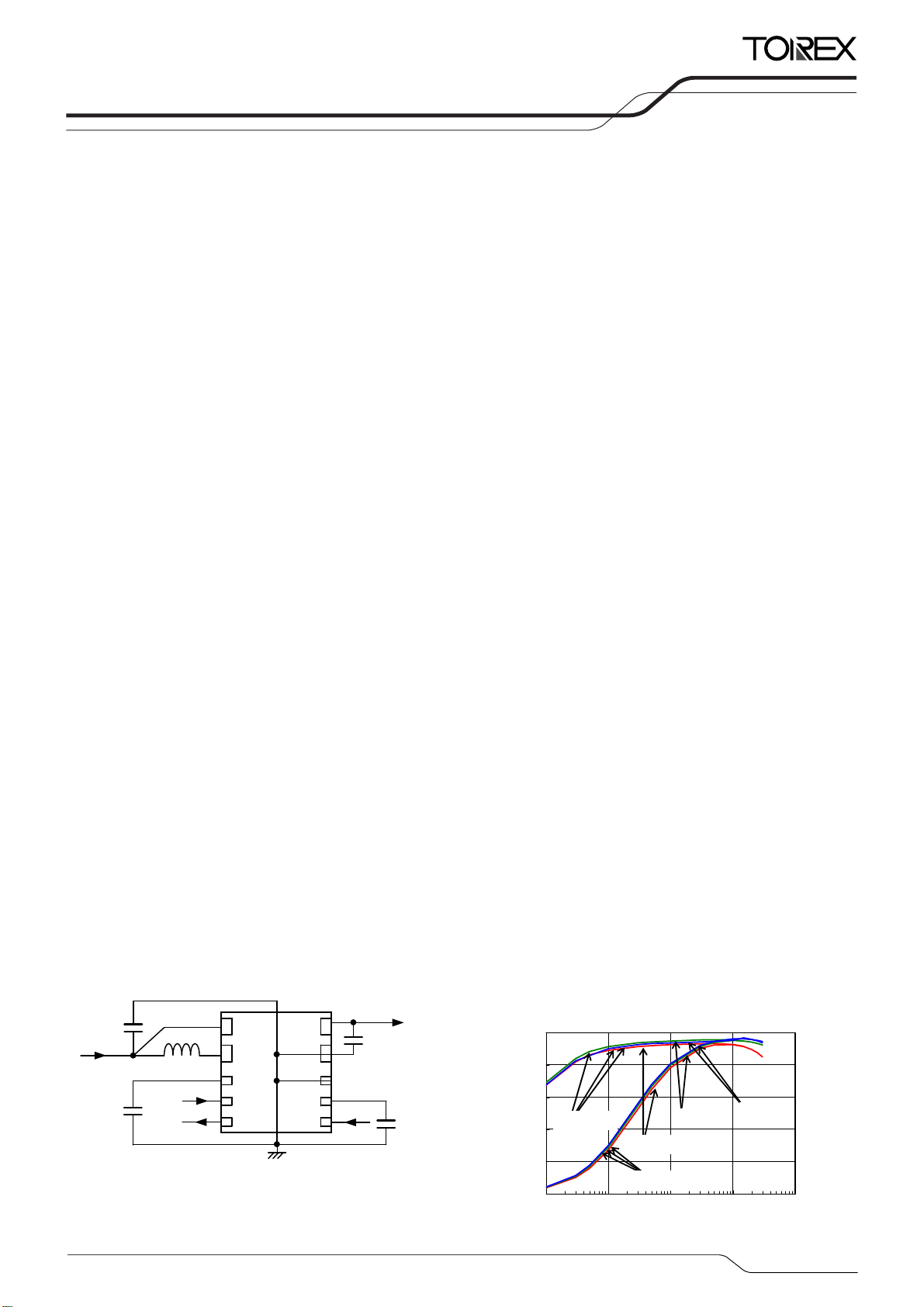
■TYPICAL APPLICATION CIRCUIT
●XC9135 Series
C
IN
V
IN
C
DD
L
MODE
V
BAT
Lx
CDD
MODE
FO
FO
V
OUT
PGND
AGND
CDF
EN
OUT
C
L
EN
Cdf
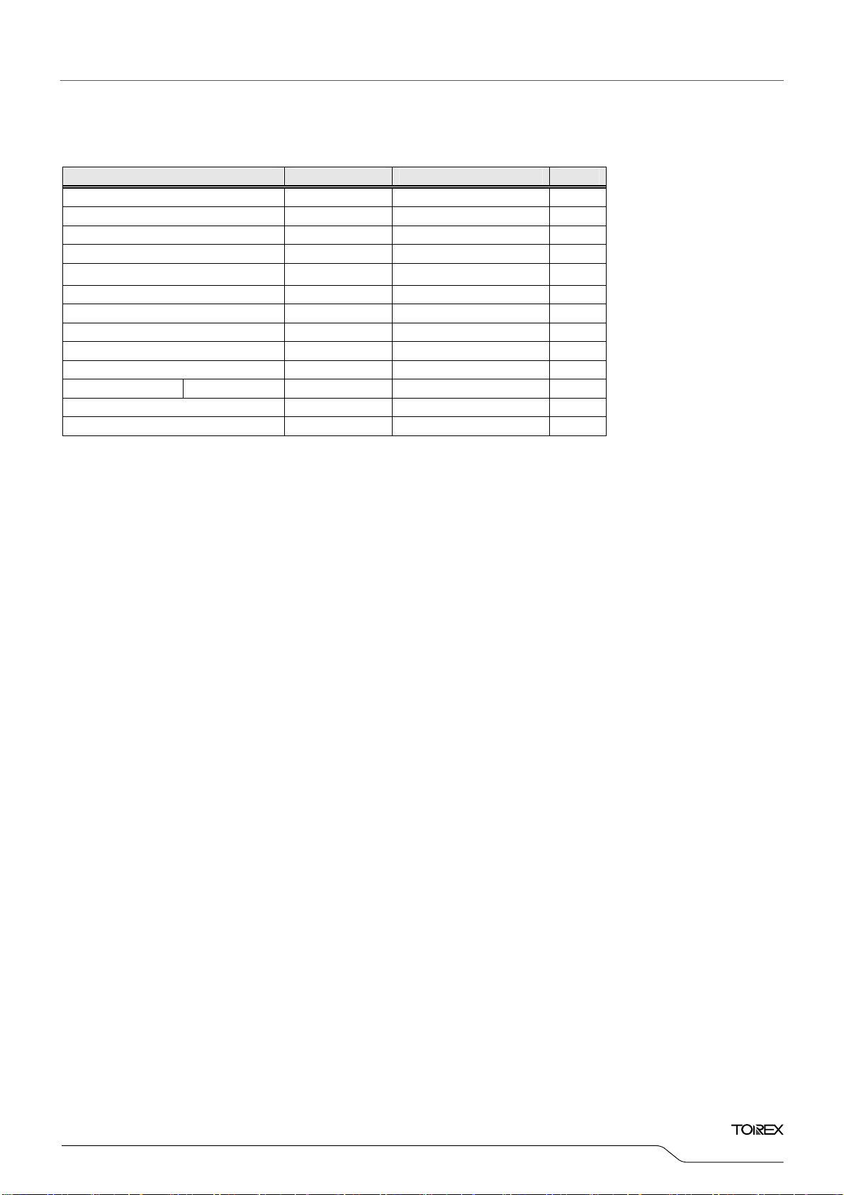
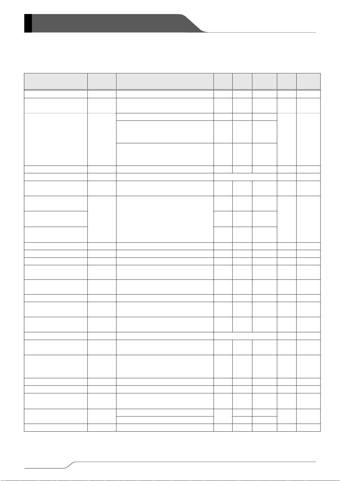
■FEATURES
Input Voltage Range
Fixed Output Voltages
Oscillation Frequency
Input Current
Output Current
Control Mode Selection
Load Transient Response
Protection Circuits
Over-current limit
Integral latch method
Functions
Load Disconnection Function
UVLO
Output Capacitor
Operating Ambient Temperature : -40℃ ~ +85℃
Package
Environmentally Friendly
■TYPICAL PERFORMANCE
CHARACTERISTICS
●Efficiency vs. Output Current
XC9135C32CDR-G (V
L=4.7μH (VLF3014ST-4R7M1R1), CL=22μF (LMK316ABJ226ML)
C
=10μF (JMK212ABJ106KG), CDD=0.47μF (TMK107BJ474KA)
IN
100
80
60
PWM/PFM
40
Efficiency : EFFI (%)
20
0
0.1 1 10 100 1000
Output Current : IOUT (mA)
☆GreenOperation Compatible
: 0.65V~5.5V
: 1.8V~5.0V(0.1V increments)
: 1.2MHz(±15%)
: 1.0A
: 500mA @ V
: PWM or Auto PWM/PFM
:
100mV V
OUT
: Thermal shutdown
: Soft-start
CL Auto Discharge Function
Flag-out Function
: Ceramic Capacitor
: USP-10B
: EU RoHS Compliant, Pb Free
=3.2V)
OUT
2.5V
VIN=1.8V
PWM
ETR0416-001a
=3.3V, VIN=1.8V(TYP.)
OUT
=3.3V,VIN=1.8V,I
3.0V
f
OSC
OUT
=1.2MHz
=1mA→200mA
1/35
XC9135/9136 Series
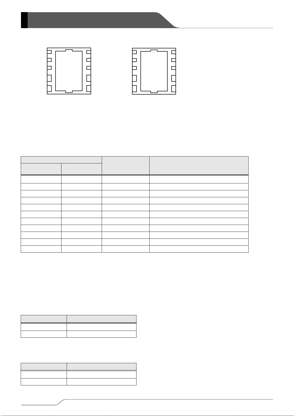
■PIN CONFIGURATION
FO
MODE
CDD
BAT
5
3
2
Lx
1
USP-10B
(BOTTOMVIEW)
XC9135シリーズ
XC9135 Series XC9136 Series
■PIN ASSIGNMENT
PIN NUMBER
XC9135 series XC9136 series
6
74
8
9
10
EN
CDF
AGND
PGND
VOUT
FO
CDD
BAT
3
2
Lx
1
USP-10B
(BOTTOMVIEW)
XC9136シリーズ
65
74
8
9
10
EN
NCMODE
AGND
PGND
VOUT
PIN NAME FUNCTIONS
1 1 BAT
2 2 Lx
3 3 CDD
Bypass Capacitor Connection
4 4 MODE
5 5 FO
6 6 EN
7 - CDF
UVLO Detect Delay Capacitor Connection
- 7 NC
8 8 AGND
9 9 PGND
10 10 VOUT
* The dissipation pad for the USP-10B package should be solder-plated in recommended mount pattern and metal masking so as to enhance
mounting strength and heat release.
If the pad needs to be connected to other pins, it should be
*Please short the GND pins (pins 8 and 9).
connected to the AGND (No.8) or PGND (No.9) pin.
Power Input
Switching
Mode Switching
Flag Output
Enable
No Connection
Analog Ground
Power Ground
Output Voltage
■FUNCTION CHART
1. EN Pin Function
XC9135/XC9136 series
EN PIN FUNCTIONS
H Operation
L Stop
* Do not leave the EN pin open.
2. MODE Pin Function
XC9135/XC9136 series
MODE PIN FUNCTIONS
H PWM
L PWM/PFM automatic control
* Do not leave the MODE pin open.
2/35
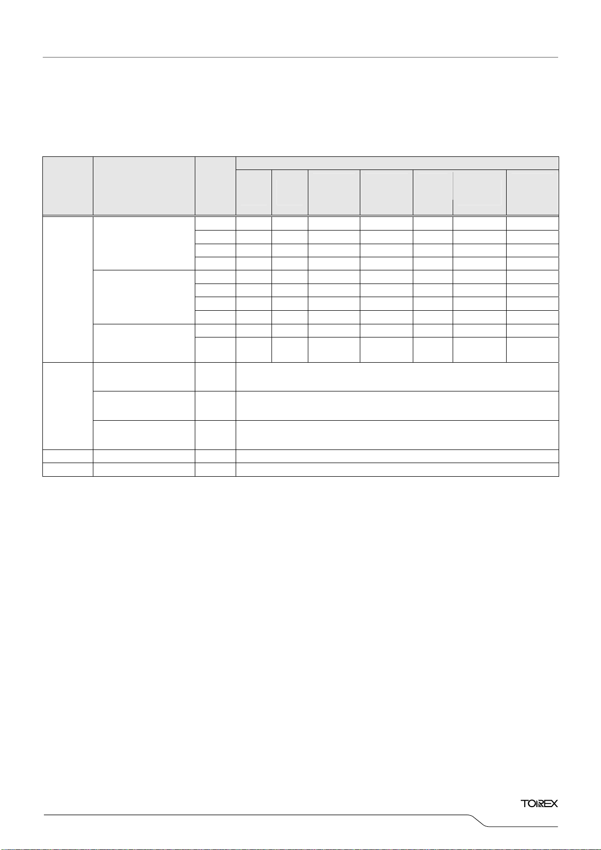
■PRODUCT CLASSIFICATION
●Ordering Information
XC9135①②③④⑤⑥-⑦
XC9136①②③④⑤⑥-⑦
DESIGNATOR
(*1)
・・・・・・・・・・・・・・V
(*1)
・・・・・・・・・・・・・・V
ITEM
product with UVLO integral latch protection
OUT
product
OUT
SYMBOL
UVLO
0.85V
DESCRIPTION
UVLO
UVLO≦1.2V
1.6V
XC9135/XC9136
(*2)
(○・・・With the functions ×・・・Without the functions)
UVLO
DETECT
DELAY
Outside
Standard
UVLO>1.2V
Outside
Standard
LATCH
PROTECTION
Series
CL
AUTO
DISCHARGE
(*3)
①
②③
④
⑤⑥-⑦
XC9135 series
Output voltage
internally fixed(V
OUT
)
A
C
B
K
L
XC9135 series
Semi custom
(*5)
M
R
T
XC9136 series
Output voltage
internally fixed(V
Output Voltage (V
OUT
OUT
)
)
(XC9135A,C Series)
Output Voltage (V
OUT
)
(XC9135B,K/XC9136 Series)
Output Voltage (V
OUT
)
(XC9135L,M,R,T Series)
E
N
28~50
18~50
01~99
Oscillation Frequency C 1.2MHz
(*1)
Package (Order Unit) DR-G
× ○ × × ○ ○ ○
× ○ × × ○ ○ ×
○ × × × ○ ○ ○
○ × × × ○ ○ ×
× × × ○ ○ ○ ○
× × × ○ ○ ○ ×
× × ○ × ○ ○ ○
× × ○ × ○ ○ ×
× × × × × × ○
× × × × × × ×
Output Voltage
e.g. V
OUT
Output Voltage
e.g. V
OUT
Semi custom serial numbers starting from 01
USP-10B (3,000/Reel)
(*4)
=5.0V⇒②=5, ③=0
(*4)
=1.8V⇒②=1, ③=8
(*6)
(*5)
(*1)
The ”-G” suffix indicates that the products are Halogen and Antimony free as well as being fully RoHS compliant.
(*2)
The SYMBOL of DESIGNATOR① is decided by the combination of with or without “UVLO”, “UVLO DETECT DELAY”, “FO”,
“LATCH PROTECTION”, and “C
Example: ○・・・With the functions ×・・・Without the functions
(*3)
Example: ○・・・V
(*4)
The XC9135A, XC9135C, XC9135L, XC9135M limit their selection rang in 2.8V to 5V. The other products have the range from 1.8V to 5V.
(*5)
The XC9135L, XC9135M, XC9135R, XC9135T are semi-custom products. Please consult with your Torex sales contact.
(*6)
The XC9135/XC9136 reels are shipped in a moisture-proof packing.
×・・・V
pin can not be connected to the different output pin such as another supply (AC adaptor).
OUT
pin can be connected to the different output pin such as another supply (AC adaptor).
OUT
DISCHARGE”.
L
The package should only be opened immediately before use. When storage time after the open is long, or receiving the device without the
moisture-proof packing in some reason, please bake the device in 60℃/24h(1 time) for removing moisture before use.
3/35
XC9135/9136 Series
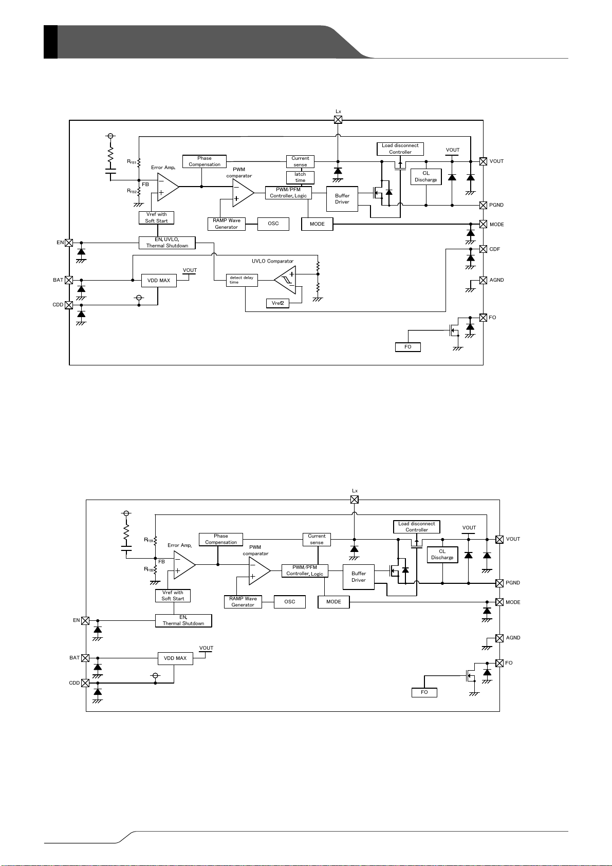
■BLOCK DIAGRAMS
●XC9135A/XC9135B/XC9135L/XC9135R Series
* Diodes inside the circuit are an ESD protection diode and a parasitic diode.
●XC9135C/XC9135K/XC9135M/XC9135T Series
XC9135C/XC9135K/XC9135M/XC9135T series does not have C
●XC9136E Series
*Diodes inside the circuit are an ESD protection diode and a parasitic diode.
●XC9136N Series
XC9136N series does not have C
discharge function.
L
4/35
discharge function.
L
■ABSOLUTE MAXIMUM RATINGS
Ta= 2 5 ℃
PAR AMETER SYMBOL RATINGS UNITS
V
Pin Voltage V
OUT
CDD Pin Voltage V
FO Pin Voltage VFO
OUT
CDD
-0.3~7.0
-0.3~7.0
-0.3~7.0
V
V
V
FO Pin Current IFO 10 mA
CDF Pin Voltage
BAT Pin Voltage V
MODE Pin Voltage V
EN Pin Voltage VEN
Lx Pin Voltage VLx
Lx Pin Current ILx
(*1)
V
CDF
BAT
MODE
-0.3~7.0
-0.3~7.0
-0.3~7.0
-0.3~7.0
-0.3~V
±2000
OUT
+0.3
V
V
V
V
V
mA
Power Dissipation USP-10B Pd 150 mW
Operating Ambient Temperature
Storage Temperature
* AGND and PGND are standard voltage for all of the voltage.
(*1)
For only the XC9135 series. The XC9136 series does not have the CDF pin.
Topr
Tstg
-40 ~ +85 ℃
-55 ~ +125 ℃
XC9135/XC9136
Series
5/35
XC9135/9136 Series
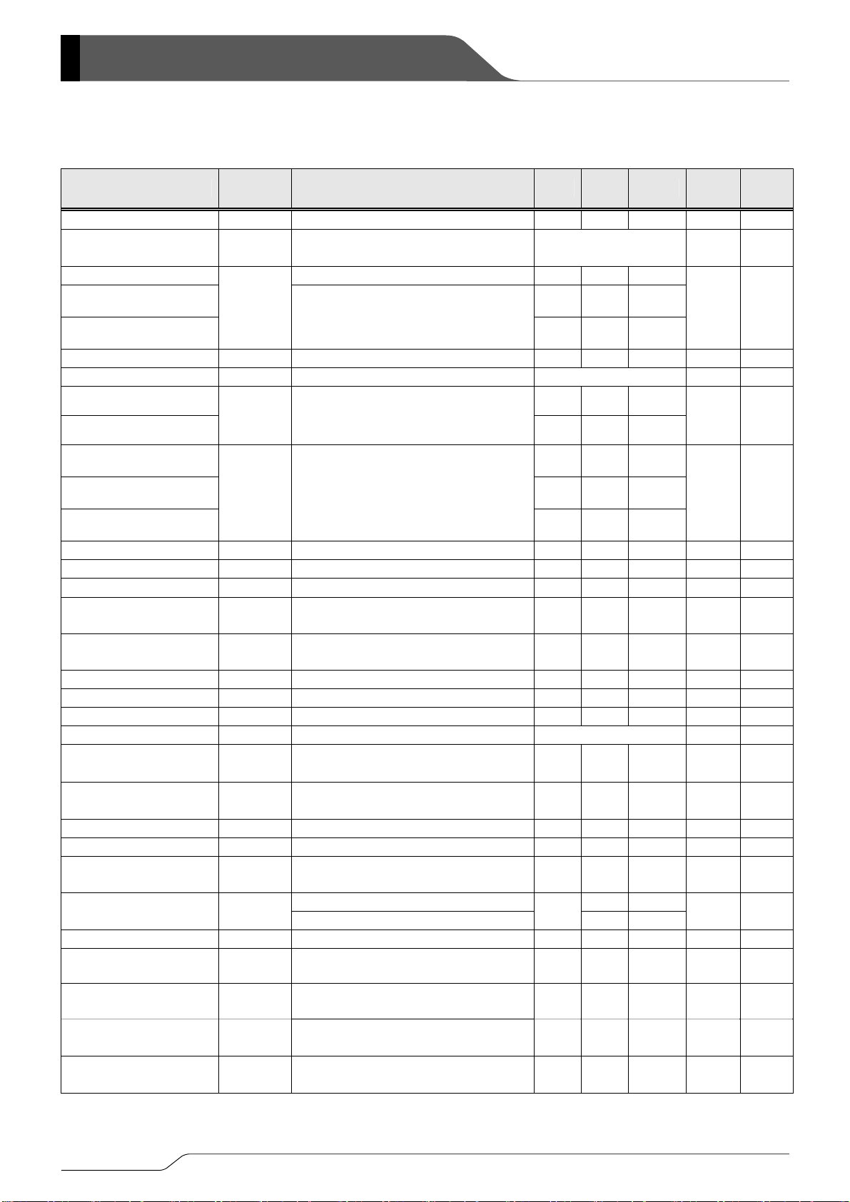
■ELECTRICAL CHARACTERISTICS
● XC9135A/XC9135C/XC9135B/XC9135K
Ta = 25 ℃
PARAMETER SYMBOL CONDITIONS MIN TYP MAX
Input Voltage VIN
Output Voltage V
OUT
V
IN=VUVLO_R(E)
R
is selected with V
L
Operation Start Voltage RL=1kΩ, V
Operation Start Voltage
XC9135A/C
Operation Start Voltage
XC9135B/K
Operation Hold Voltage V
V
ST1
HLD
V
=0V,
MODE
V
≦3.3V,I
OUT(E)
V
>3.3V,I
OUT(E)
RL=1kΩ, V
+0.1V
, Refer to F1 Table
OUT(E)
=0V
MODE
=100mA
OUT
=50mA
OUT
=0V
MODE
5.5 V
E1 V
Supply Current Iq E2
Input Pin Current
XC9135A/C
Input Pin Current
XC9135B/K
Stand-by Current
XC9135A
Stand-by Current
XC9135B
Stand-by Current
XC9135C/K
Lx Leakage Current I
Oscillation Frequency f
Maximum Duty Cycle D
Minimum Duty Cycle D
PFM Switching Current I
Efficiency
(*2)
EFFI I
Lx SW "Pch" ON Resistance R
Lx SW "Nch" ON Resistance
Maximum Current Limit I
Integral Latch Time t
Soft-Start Time tSS
Thermal Shut Temperature T
Hysteresis Width T
CL Discharge Resistance
XC9135A/B
(*8)
R
FO ON Resistance RFO
FO Leakage Current I
FO_LEAK
EN "H" Voltage V
EN "L" Voltage V
MODE "H" Voltage V
MODE "L" Voltage V
I
VIN=V
BAT
I
VIN=V
STB
VIN=VLx=V
LxL
OSC
MAX
MIN
PFM
LxP
R
LxN
LIM
LAT
V
IN=Vpull
V
IN=Vpull
V
IN=VOUT(E)
R
L
V
MODE
R
L
OUT
I
OUT
(*4)
E3 A
V
IN
from becoming FO=”H”
VIN=V
After V
TSD
HYS
DCHG
VIN=V
VEN=3.3V, VFO=0.5V,V
V
EN
-0.2V, VEN=3.3V
OUT(E)
OUT(E)
0.1 2.0
OUT(E)
=(V
OUT(E)+VUVLO_R(E)
=(V
OUT(E)+VUVLO_R(E)
)/2
)/2
+0.5V,
is selected with V
, Refer to F1 Table
OUT(E)
=0V,
is selected with V
=100mA,V
=200mA
MODE
(*3)
0.20
, Refer to F1 Table
OUT(E)
=0V,VFO:OPEN 93 %
=(V
)/2, time to stop Lx oscillation
OUT(E)
=(V
pull
OUT(E)+VUVLO_R(E)
=0V→3.3V, time to FO=L
EN
(*5)
=2.0V
OUT
=3.3V, VFO=0.5V,V
)/2, V
OUT=VOUT(E)
100 200 400 Ω
<3.3V
OUT(E)
≧3.3V
OUT(E)
(*6)
(*6)
×0.95
VFO=5.5V 0 1
ENH
ENL
MODEH
MODEL
=(V
V
IN=Vpull
While VEN=0.20V→0.75V, Voltage to start oscillation
V
IN=Vpull
While VEN=0.75V→0.20V, Voltage to stop oscillation
Voltage for PWM Control
R
is selected with V
L
Voltage for PFM Control
is selected with V
R
L
OUT(E)+VUVLO_R(E)
=(V
OUT(E)+VUVLO_R(E)
)/2,
)/2,
, Refer to F1 Table
OUT(E)
, Refer to F1 Table
OUT(E)
1.1 4.0
1.5 6.0
0.2 3.5
0.2 4.5
1.0 6.0
1.02 1.20 1.38 MHz
86.5 93.0 98.0 %
0 %
250 350 mA
0.5 2.0 4.0 ms
2.6 5.0 8.5 ms
150
20
100
0.75 5.5 V
AGND 0.2 V
0.75 5.5 V
AGND 0.2 V
6/35
V
V
UVLO_R
0.9
V
UVLO_F
0.35
(*1)
0.20
0.35
200 250
150 200
UNITS CIRCUIT
UVLO_R
(*1)
V
(*1)
V
μA ②
μA ⑥
μA ③
μA ④
(*1)
Ω ⑧
(*1)
Ω ⑨
℃
℃
Ω
μA ⑦
①
①
①
⑤
⑤
①
①
①
①
①
⑤
⑥
⑦
⑤
⑤
①
①
XC9135/XC9136
■ELECTRICAL CHARACTERISTICS (Continued)
● XC9135A/XC9135C/XC9135B/XC9135K
PARAMETER SYMBOL CONDITIONS MIN TYP MAX UNITS CIRCUIT
Series
Ta = 25 ℃
EN "H" Current I
EN "L" Current I
MODE "H" Current I
MODE "L" Current I
UVLO Release Voltage
XC9135A/C
UVLO Release Voltage
XC9135B/K
UVLO Hysteresis Width
XC9135A/C
UVLO Hysteresis Width
XC9135B/K
Output Voltage Drop
Protection
XC9135B/K
(*9)
UVLO
Detect Delay
VIN=VEN=5.5V 0.1
ENH
VIN=5.5V,VEN=0V -0.1
ENL
VIN=VEN=V
MODEH
VIN=VEN=5.5V,V
MODEL
V
UVLO_R
RL=1kΩ,While VIN=0.2V→3.3V,
Voltage to start oscillation
=5.5V 0.1
MODE
=0V -0.1
MODE
1.552 1.600 1.648
0.799 0.850 0.901
0.10
(*7)
V
UVLO_HYS
0.05
V
LVP
tDF
While V
oscillation
After V
0.65V,
=1.7V → 1.3V, Voltage to stop
OUT
IN=VPULL
=(V
OUT(E)+VUVLO_R(E)
)/2→
1.4 1.5 1.6
0.5 1.0 1.5
time to stop oscillation
0.14 0.20
External Components: C
=10μF(ceramic), L=2.2μH(VLCF4020 TDK), CDD=0.47μF(ceramic),CL=22μF(ceramic), CDF=1000pF(ceramic)
IN
Test Conditions
For the Circuit No.1, unless otherwise stated, V
For the Circuit No.2, unless otherwise stated, V
For the Circuit No.3, unless otherwise stated, V
For the Circuit No.4, unless otherwise stated, V
For the Circuit No.5, unless otherwise stated, V
For the Circuit No.6, unless otherwise stated, V
For the Circuit No.7, unless otherwise stated, V
For the Circuit No.8, unless otherwise stated, V
For the Circuit No.9, unless otherwise stated, V
=(V
IN
OUT(E)+VUVLO_R(E)
IN=VEN=VOUT(E)
OUT=VEN=VMODE
OUT=VEN=VMODE
=1.5V, V
IN=Vpull
OUT=VOUT(E)
IN=VOUT(E)
IN=VLX=VOUT(E)
=1.1V,V
IN
+0.5V, VEN=V
+0.5V, VEN=V
OUT
)2,VEN=V
+0.5V, V
MODE=VFO
=0V(GND connected),CDF:OPEN
MODE
=0V(GND connected),CDF:OPEN
=0V(GND connected),CDF:OPEN
OUT=VEN=VMODE=VFO=VOUT(E)-
=0V(GND connected),CDF:OPEN
MODE
=0V(GND connected),CDF:OPEN
MODE
+0.5,VEN=V
=1.6V,VEN=3.3V,V
=3.3V,CDF:OPEN
MODE
MODE=VFB(CDF
= Output Voltage Setting V
V
OUT(E)
V
UVLO_F=VUVLO_R-VUVLO_HYS
=UVLO Voltage Setting
UVLO_R(E)
(*1) Designed value
(*2) Efficiency =[{(output voltage) X (output current)} ÷ {(input voltage) X (input current)} ] X 100
SW "P-ch" ON resistance=(VLx-V
(*3) L
X
(*4) Testing method of L
(*5) C
Discharge resistance
L
(*6) FO ON resistance = V
SW "N-ch" ON resistance is stated at test circuits.
X
= V
÷ V
OUT
÷ FO pin measure current
FO
(*7) The Voltage is a difference between V
(*8) The XC9135C,XC9135K series does not have C
pin test voltage)÷200mA
OUT
pin measure current
OUT
and the voltage to stop oscillation for Lxpin while VIN=V
UVLO_R
discharge function. For XC9135A, XC9135B.
L
(*9) The XC9135A,XC9135C series does not have output voltage drop protection. For XC9135B, XC9135K.
=3.3V
→0.2V.RL=1kΩ
UVLO_R
μA ②
μA ②
μA ②
μA ②
V ①
V ①
V ⑤
ms ⑤
0.1V,
)=0V(GND connected)
7/35
XC9135/9136 Series
■ELECTRICAL CHARACTERISTICS (Continued)
●XC9136E/XC9136N
PARAMETER SYMBOL CONDITIONS MIN TYP MAX UNITS CIRCUIT
Ta =2 5 ℃
Input Voltage VIN
Output Voltage V
Operation Start Voltage V
Operation Hold Voltage V
RL is selected with V
OUT
RL=1kΩ, V
V
MODE
ST1
HLD
V
OUT(E)
V
OUT(E)
RL=1kΩ, V
MODE
=0V,
≦3.3V,I
>3.3V,I
MODE
, Refer to F1 Table E1 V
OUT(E)
=0V 0.85
=100mA
OUT
=50mA
OUT
=0V 0.65 V
5.5 V
Supply Current Iq 36 52
Input Pin Current I
Stand-by Current
XC9136E
Stand-by Current
XC9136N
Lx Leakage Current I
Oscillation Frequency f
Maximum Duty Cycle D
Minimum Duty Cycle D
PFM Switching Current I
Efficiency
(*2)
EFFI
Lx SW "Pch" ON Resistance R
VIN=V
BAT
-0.2V, VEN=3.3V 0.65 2.15
OUT(E)
0.1 2.0
I
VIN=V
STB
OUT(E)
0.9 5.0
VIN=VLx=V
LxL
VIN=V
OSC
86.5 93.0 98.0 %
MAX
MIN
PFM
I
LxP
pull=VOUT(E)
V
IN=VOUT(E)
R
is selected with V
L
=0V,
V
MODE
R
is selected with V
L
=(V
V
IN
I
=100mA,V
OUT
=200mA
OUT
0.1 2.0
OUT(E)
/2 1.02 1.20 1.38 MHz
+0.5V,
OUT(E)
, Refer to F1 Table
OUT(E)
, Refer to F1 Table
OUT(E)
+0.85V)/2,
=0V,VFO:OPEN
MODE
(*3)
0.20
0 %
250 350 mA
93 %
0.9
0.35
(*1)
(*1)
①
V
①
①
μA ②
μA ⑥
μA ③
μA ④
⑤
⑤
①
①
①
Ω
⑧
Lx SW "Nch" ON Resistance R
Maximum Current Limit I
Soft-Start Time tSS
Thermal Shut Temperature T
Hysteresis Width T
CL Discharge Resistance
XC9136E
(*7)
FO ON Resistance RFO
FO Leakage Current I
EN "H" Voltage V
EN "L" Voltage V
MODE "H" Voltage V
MODE "L" Voltage V
EN "H" Current I
EN "L" Current I
MODE "H" Current I
MODE "L" Current I
(*4)
LxN
LIM
TSD
HYS
R
DCHG
FO_LEAK
ENH
ENL
MODEH
MODEL
VIN=VEN=5.5V 0.1
ENH
VIN=5.5V,VEN=0V -0.1
ENL
MODEH
MODEL
V
IN
V
IN=Vpull
V
EN
=(V
+0.85V)/2
OUT(E)
=1.6V, V
OUT=VOUT(E)
×0.95
=0V→3.3V, voltage to start oscillation
2.6 5.0 8.5 ms
VIN=V
OUT
VEN=3.3V, VFO=0.5V,V
=3.3V, VFO=0.5V,V
V
EN
=2.0V
(*5)
100 200 400 Ω
(*6)
OUT(E)
OUT(E)
<3.3V
≧3.3V
(*6)
100
VFO=5.5V 0 1
V
=1.6V,
IN=Vpull
While VEN=0.20V→0.75V, Voltage to start oscillation
V
=1.6V,
IN=Vpull
While VEN=0.75V→0.20V, Voltage to stop oscillation
Voltage for PFM Control
R
is selected with V
L
Voltage for PWM Control
R
is selected with V
L
VIN=VEN=V
MODE
VIN=VEN=5.5V,V
=5.5V 0.1
MODE
, Refer to F1 Table
OUT(E)
, Refer to F1 Table
OUT(E)
=0V -0.1
0.75 5.5 V ⑤
AGND 0.2 V ⑤
0.75 5.5 V ①
AGND 0.2 V ①
0.20
(*1)
E3 A
150
20
200 250
150 200
(*1)
0.35
Ω
⑨
①
⑤
℃
℃
⑥
Ω
⑦
μA ⑦
μA ②
μA ②
μA ②
μA ②
8/35

■ELECTRICAL CHARACTERISTICS (Continued)
●XC9136E/XC9136N
External Components: CIN=10μF(ceramic), L=2.2μH(VLCF4020 TDK), CDD=0.47μF(ceramic),CL=22μF(ceramic)
Test Conditions
For the Circuit No.1, unless otherwise stated, Circuit No.1 V
For the Circuit No.3, unless otherwise stated, V
For the Circuit No.4, unless otherwise stated, V
For the Circuit No.5, unless otherwise stated, V
For the Circuit No.6, unless otherwise stated, V
For the Circuit No.7, unless otherwise stated, V
For the Circuit No.8, unless otherwise stated, V
For the Circuit No.9, unless otherwise stated, V
For the Circuit No.2, unless otherwise stated, Circuit No.2 VIN=VEN=V
OUT=VEN=VMODE
OUT=VEN=VMODE
IN=Vpull
OUT=VOUT(E)
IN=VOUT(E)
IN=VLX=VOUT(E)
=1.1V,V
IN
=1.6V,VEN=V
IN
OUT(E)
=0V(GND connected)
=0V(GND connected)
=1.5V, V
OUT=VEN=VMODE=VFO=VOUT(E)-
+0.5V, VEN=V
+0.5V, VEN=V
+0.5,VEN=V
=1.6V,VEN=3.3V,V
OUT
+
0.5V, V
= Output Voltage Setting
V
OUT(E)
(*1) Designed value
(*2) Efficiency =[{(output voltage) X (output current)} ÷ {(input voltage) X (input current)}] X 100
SW "P-ch" ON resistance=(VLx-V
(*3) L
X
(*4) Testing method of L
(*5) C
Discharge resistance
L
(*6) FO ON resistance = V
SW "N-ch" ON resistance is stated at test circuits.
X
= V
÷ V
OUT
÷ FO pin measure current
FO
(*7) The XC9136NSeries does not have C
pin test voltage)÷200mA
OUT
pin measure current
OUT
discharge function. For XC9136E.
L
=3.3V
MODE
=0V(GND connected)
MODE
=0V(GND connected)
MODE
=0V
MODE
=3.3V
MODE
=0V(GND connected)
MODE
XC9135/XC9136
Series
0.1V
9/35
XC9135/9136 Series
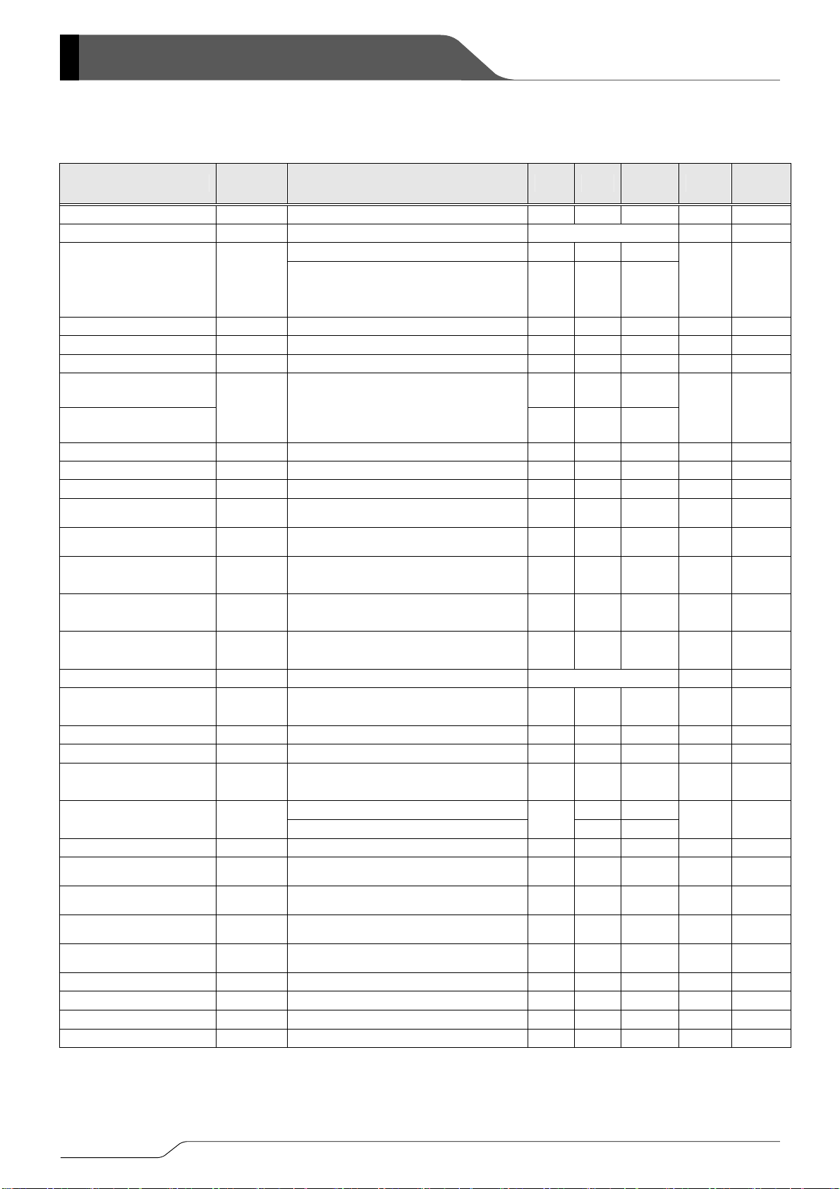
■ELECTRICAL CHARACTERISTICS (Continued)
●XC9135L/XC9135M/XC9135R/XC9135T
PARAMETER SYMBOL CONDITIONS MIN TYP MAX UNITS CIRCUIT
Ta =2 5 ℃
Input Voltage VIN 5.5 V
Output Voltage Accuracy
(*10)
V
Operation Start Voltage V
Operation Hold Voltage V
OUT
R
is selected with V
L
V
IN=VUVLO_R(E)
RL=1kΩ, V
V
MODE
V
OUT(E)
V
ST1
HLD
OUT(E)
V
MODE
V
OUT(E)
V
OUT(E)
RL=1kΩ, V
MODE
=0V,V
≦3.3V,I
>3.3V,I
=0V,V
≦3.3V,I
>3.3V,I
MODE
+0.1V
, Refer to F1 Table
OUT(E)
-2 2 %
=0V V
≧1.0,
UVLO_R(E)
=100mA
OUT
=50mA
OUT
<1.0,
UVLO_R(E)
=100mA
OUT
=50mA
OUT
=0V V
V
UVLO_F
V
Current Limit Iq E2
Input Pin Current I
Stand-by Current
XC9135L
Stand-by Current
XC9135R
Stand-by Current
XC9135M/T
Lx Leakage Current I
Oscillation Frequency f
Maximum Duty Cycle D
Minimum Duty Cycle D
PFM Switching Current I
Efficiency
(*2)
EFFI I
Lx SW "Pch" ON Resistance R
VIN=V
BAT
I
VIN=V
STB
VIN=VLx=V
LxL
I
V
V
V
R
V
R
OUT
OUT
OSC
MAX
MIN
PFM
LxP
-0.2V, VEN=3.3V 1.1 6.0
OUT(E)
OUT(E)
0.1 2.0
OUT(E)
=(V
IN=Vpull
IN=Vpull
IN=VOUT(E)
is selected with V
L
MODE
is selected with V
L
OUT(E)+VUVLO_R(E)
=(V
OUT(E)+VUVLO_R(E)
+0.5V
=0V,
=100mA,V
=200mA
MODE
(*3)
0.20
0.2 3.5
0.2 4.5
1.0 6.0
)/2
)/2
, Refer to F1 Table
OUT(E)
, Refer to F1 Table
OUT(E)
1.02 1.20 1.38 MHz
86.5 93.0 98.0 %
0 %
250 350 mA
=0V,VFO:OPEN 93 %
UVLO_R
UVLO_R
0.9
0.35
(*1)
(*1)
(*1)
V
μA ②
μA ⑥
μA ③
μA ④
Ω
①
①
①
⑤
⑤
①
①
①
⑧
Lx SW "Nch" ON Resistance R
Maximum Current Limit I
Integral Latch Time t
Soft-Start Time tSS
Thermal Shut Temperature T
Hysteresis Width T
CL Discharge Resistance
XC9135L/R
(*8)
FO ON Resistance RFO
FO Leakage Current I
10/35
(*4)
LxN
E3 A
LIM
LAT
150
TSD
20
HYS
R
DCHG
FO_LEAK
V
=(V
IN
becoming FO=”H”.
V
IN=Vpull
V
OUT=VOUT(E)
After V
VIN=V
VEN=3.3V, VFO=0.5V,V
V
EN
)/2, time to stop Lx oscillation from
OUT(E)
=(V
OUT(E)+VUVLO_R(E)
)/2,
×0.95
=0V→3.3V, time to start FO=L.
EN
(*5)
=2.0V
OUT
=3.3V, VFO=0.5V,V
100 200 400 Ω
<3.3V
OUT(E)
≧3.3V
OUT(E)
(*6)
(*6)
0.5 2.0 4.0 ms
2.6 5.0 8.5 ms
100
VFO=5.5V 0 1
0.20
(*1)
0.35
200 250
150 200
(*1)
Ω
℃
℃
Ω
μA ⑦
⑨
①
①
⑤
⑥
⑦
XC9135/XC9136
■ELECTRICAL CHARACTERISTICS (Continued)
●XC9135L/XC9135M/XC9135R/XC9135T
PARAMETER SYMBOL CONDITIONS MIN TYP MAX UNITS CIRCUIT
Series
Ta =2 5 ℃
EN "H" Voltage V
EN "L" Voltage V
MODE "H" Voltage V
MODE "L" Voltage V
EN "H" Current I
EN "L" Current I
MODE "H" Current I
MODE "L" Current I
UVLO Release Voltage V
Hysteresis Width
V
Output Voltage Drop
Protection
XC9135R/T
(*9)
UVLO Detect Delay tDF
=(V
V
ENH
ENL
MODEH
MODEL
ENH
ENL
MODEH
MODEL
UVLO_R
UVLO_HYS
V
LVP
While VEN=0.20V→0.75V, Voltage to start oscillation
V
IN=Vpull
While VEN=0.75V→0.20V, Voltage to stop oscillation
Voltage for PFM Control
R
is selected with V
L
Voltage for PWM Control
R
is selected with V
L
VIN=VEN=5.5V 0.1
VIN=5.5V,VEN=0V -0.1
VIN=VEN=V
VIN=VEN=5.5V,V
R
=1kΩ,While VIN=0.2V→3.3V,
L
Voltage to start oscillation
(*7)
(*7)
While V
oscillation
IN=Vpull
After V
OUT(E)+VUVLO_R(E)
=(V
OUT(E)+VUVLO_R(E)
=5.5V 0.1
MODE
MODE
0.9≦V
2.0<V
OUT
IN
UVLO_R(E
=(V
≦2.0
UVLO_R(E
)
≦3.0
)
=1.7V→1.3V, Voltage to stop
OUT(E)+VUVLO_R(E)
time to stop oscillation
)/2,
)/2,
, Refer to F1 Table
OUT(E)
, Refer to F1 Table
OUT(E)
0.75 5.5 V
AGND 0.2 V
0.75 5.5 V
AGND 0.2 V
=0V -0.1
0.10 UVLO
0.05
1.4 1.5 1.6
)/2→0.65V,
0.5 1.0 1.5
External Components
Test Conditions
For the Circuit No.3, unless otherwise stated, V
For the Circuit No.4, unless otherwise stated, V
For the Circuit No.5, unless otherwise stated, V
For the Circuit No.6, unless otherwise stated, V
For the Circuit No.7, unless otherwise stated, V
For the Circuit No.8, unless otherwise stated, V
For the Circuit No.9, unless otherwise stated, V
= Output Voltage Setting V
V
OUT(E)
V
UVLO_F=VUVLO_R-VUVLO_HYS
(*1) Designed value
(*2) Efficiency =[ {(output voltage) X (output current)} ÷ {(input voltage) X (input current)} ] X 100
SW "P-ch" ON resistance=(VLx-V
(*3) L
X
(*4) Testing method of L
(*5) C
Discharge resistance
L
(*6) FO ON resistance = V
(*7) The Voltage is a difference between V
(*8) The XC9135M,XC9135T series does not have C
(*9) The XC9135L,XC9135M series does not have output voltage drop protection. For XC9135R, XC9135T.
CIN=10μF(ceramic), L=2.2μH(VLCF4020 TDK), CDD=0.47μF(ceramic),CL=22μF(ceramic), CDF=1000pF(ceramic)
:
For the Circuit No.1, unless otherwise stated, V
For the Circuit No.2, unless otherwise stated, V
=UVLO Voltage Setting
UVLO_R(E)
=(V
IN
OUT(E)+VUVLO_R(E)
IN=VEN=VOUT(E)
OUT=VEN=VMODE
OUT=VEN=VMODE
=1.5V, V
IN=Vpull
OUT=VOUT(E)
IN=VOUT(E)
IN=VLX=VOUT(E)
=1.1V,V
IN
+0.5V, VEN=V
+0.5V, VEN=V
OUT
)2,VEN=V
+0.5V, V
MODE=VFO
=0V(GND connected),CDF:OPEN
MODE
=0V(GND connected),CDF:OPEN
=0V(GND connected),CDF:OPEN
OUT=VEN=VMODE=VFO=VOUT(E)-
=0V(GND connected),CDF:OPEN
MODE
=0V(GND connected),CDF:OPEN
MODE
+0.5,VEN=V
=1.6V,VEN=3.3V,V
=3.3V,CDF:OPEN
MODE
MODE=VFB(CDF
pin test voltage)÷200mA
OUT
SW "N-ch" ON resistance is stated at test circuits.
X
= V
÷ V
OUT
÷ FO pin measure current
FO
pin measure current
OUT
and the voltage to stop oscillation for Lxpin while VIN=V
UVLO_R
discharge function. For XC9135L, XC9135R.
L
E4
0.14 0.20
=3.3V
0.1V,
)=0V(GND connected)
→0.2V.RL=1kΩ
UVLO_R
⑤
⑤
①
①
μA ②
μA ②
μA ②
μA ②
V ①
V ①
V ⑤
ms ⑤
11/35
 Loading...