

TOREX XC9128, XC9129 User Manual
)
)
F
XC9128/XC9129 Series
ETR0411-010a
1A Driver Transistor Built-In, Step-Up DC/DC Converters
■GENERAL DESCRIPTION
The XC9128/XC9129 series are synchronous step-up DC/DC converters with a 0.2 (TYP.) N-channel driver transistor and a
synchronous 0.2 (TYP.) P-channel switching transistor built-in. A highly efficient and stable current can be supplied up to
1.0A by reducing ON resistance of the built-in transistors. With a high switching frequency of 1.2MHz, a small inductor is
selectable making the series ideally suited for applications requiring low profile or space saving solutions. With the MODE
pin, the series provides mode selection of PWM control or PFM/PWM automatic switching control. In the PWM/PFM
automatic switching mode, the series switches from PWM to PFM to reduce switching loss when load current is small.
When load current is large, the series switches automatically to the PWM mode so that high efficiency is achievable over a
wide range of load conditions. The series also provides small output ripple from light to large loads by using the built-in
circuit which enables the smooth transition between PWM and PFM. With a adaptor enable function of the XC9128 series,
when a voltage higher than the input voltage is applied to the output, the input and the output become isolated making it
possible for the IC to work in parallel with the likes of an AC adaptor.
■APPLICATIONS
●Digital audio equipment
●Digital cameras, Video equipment
●Computer Mouses
●Various multi-function power supplies using alkali cells (1
to 3 cells), nickel hydride batteries, or single lithium cells
■ FEATURES
High Efficiency, Large Current Step-Up Converter
Output Current : 150mA@V
Input Voltage Range : 0.8V~6.0V
Output Voltage Setting
Range
Oscillation Frequency : 1.2MHz (Fixed oscillation frequency
Input Current : 1.0A
Maximum Current Limit : 1.2A (MIN.), 2.0A (MAX.)
Control : PWM, PWM/PFM control
High Speed
Transient Response
Protection Circuits : Thermal shutdown
Soft-Start Time : 5ms (TYP.) internally set
Ceramic Capacitor Compatible
Adaptor Enable Function (XC9128 series)
Flag Output (XC9128 series) : Open-drain output
Operating Ambient Temperature
Packages : MSOP-10, USP-10B
Environmentally Friendly
☆GreenOperation Compatible
=3.3V, VIN=0.9V
=1.8V, I
OUT
=3.3V, VIN=1.8V
OUT
=3.3V,
OUT
=10mA→100mA
OUT
500mA@V
: 1.8V~5.3V (Externally set)
Set up freely with a reference voltage
supply of 0.45V (±0.010V) & external
components
accuracy ±15%)
externally selectable
:100mV @ V
V
IN
Integral latch method (Over current
limit)
: - 40℃~+85℃
: EU RoHS Compliant, Pb Free
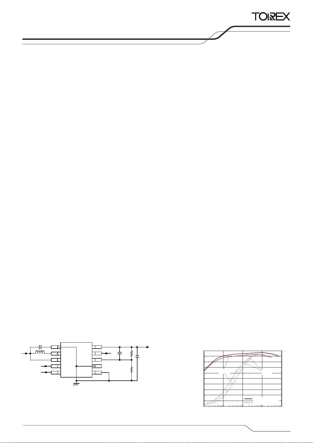
■TYPICAL APPLICATION CIRCUIT
V
C
IN
IN
L
EN
FO
PGND
1
2
Lx
BAT
3
EN
4
FO
5
VOUT
MODE
AGND
AEN/
10
MODE
C
9
FB
8
7
6
R
FB1
FB
R
FB2
V
C
L
(ceramic)
OUT
■TYPICAL PERFORMANCE
CHARACTERISTICS
●Efficiency vs. Output Current
XC9128B45CD
L=4.7μH(LTF5022-LC),CL=30μF(LMK212BJ106KG ×3
100
90
80
70
60
50
40
30
Efficiency: EFFI (%
20
10
0
0.1 1 10 100 1000
1.8V
Output Current: I
V
=3.3V,VEN=6V,VFO=OPEN,V
OUT
R
=270kΩ,R
FB1
OUT
=43kΩ,CFB=12pF,CIN=10μ
FB2
3.0V
PW M/PFM (V
PWM (V
MODE=VOUT
(mA)
MODE
=0V)
)
=0V
AEN/
1/26
XC9128/XC9129 Series
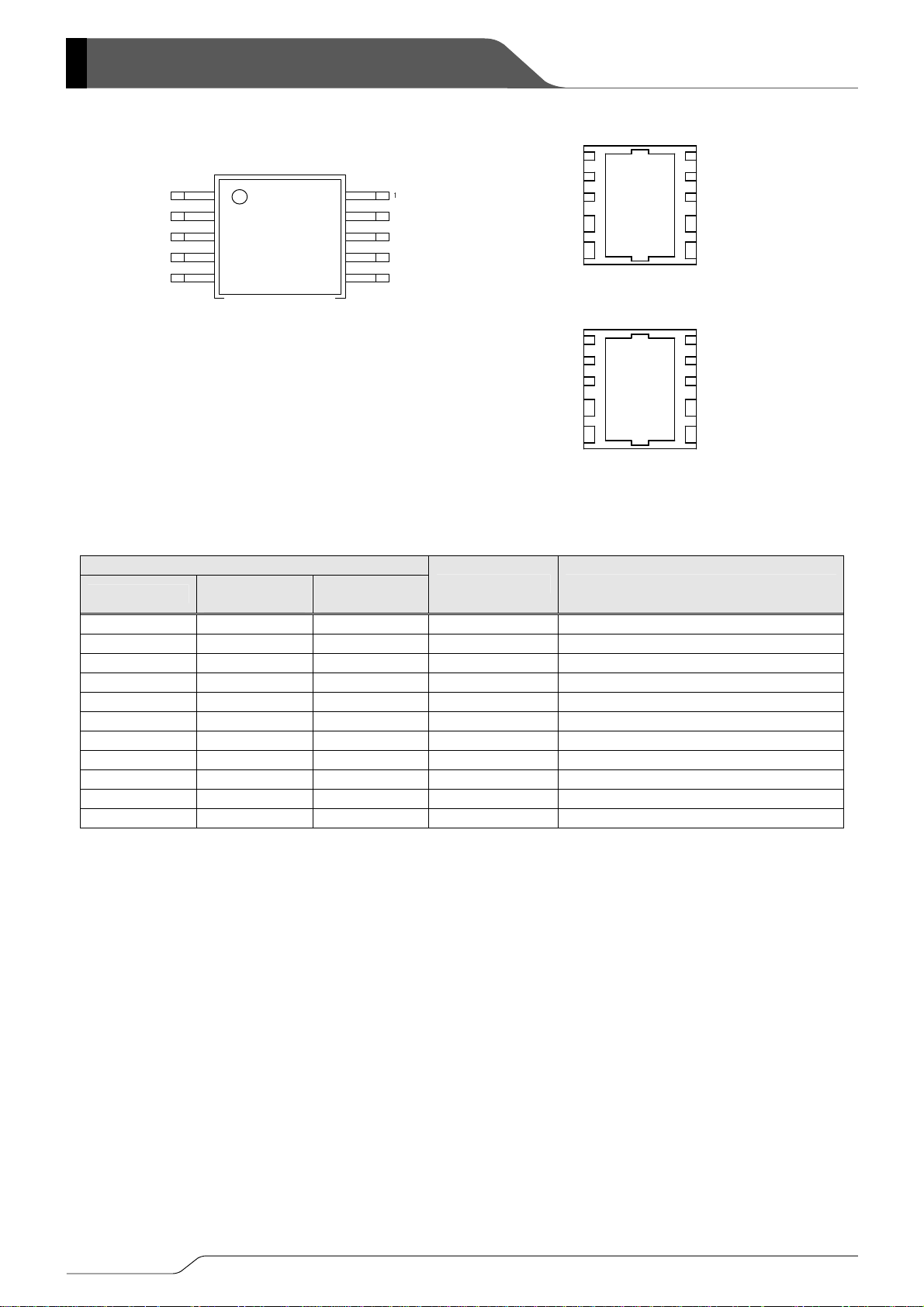
■PIN CONFIGURATION
P
1
GND
Lx 2
BAT 3
EN 4
FO 5
MSOP-10
(TOP VIEW)
■PIN ASSIGNMENT
10 V
OUT
9 MODE
8 FB
7 A
GND
6 AEN/
FO 5
EN 4
BAT 3
P
GND
NC 5
EN 4
BAT 3
P
GND
Lx 2
1
USP-10B
(BOTTOM VIEW)
XC9128 Series
Lx 2
1
USP-10B
(BOTTOM VIEW)
XC9129 Series
6 AEN/
7 A
GND
8 FB
9 MODE
10 V
OUT
6 NC
7 A
GND
8 FB
9 MODE
10 V
OUT
PIN NUMBER
MSOP-10*
USP-10B*
(XC9128)
USP-10B*
(XC9129)
PIN NAME FUNCTION
1 1 1 PGND Power Ground
2 2 2 Lx Output of Internal Power Switch
3 3 3 BAT Battery Input
4 4 4 EN Chip Enable
5 5 - FO Flag Output
6 6 - AEN/ Adaptor Enable
7 7 7 AGND Analog Ground
8 8 8 FB Output Voltage Monitor
9 9 9 MODE Mode Switch
10 10 10 VOUT Output Voltage
- - 5, 6 NC No Connection
*For MSOP-10 and USP-10B packages, please short the GND pins (pins 1 and 7).
*The dissipation pad for the USP-10B package should be solder-plated following the recommended mount pattern and metal masking
so as to enhance mounting strength and heat release. If the pad needs to be connected to other pins, it should be connected to the
Ground pins (pins 1 and 7).
2/26
■FUNCTION CHART
1. EN, AEN/ Pin Function
●XC9128 Series
EN PIN AEN/ PIN
L→H L
H H→L Lower than 0.45×0.8V Operation Available
H H→L Higher than 0.45×0.95V Operation Not Available
H H -
L L
L H
* Do not leave the EN and AEN/ Pins open.
●XC9129 Series
EN PIN IC OPERATIONAL STATE
H Operation
L Disable
* Do not leave the EN Pin open.
2. MODE Pin Function
●XC9128/XC9129 Series
MODE PIN FUNCTION
H PWM Control
L PWM/PFM Automatic Switching Control
FB PIN VOLTAGE
-
-
-
XC9128/XC9129
Series
IC OPERATIONAL STATE SOFT-START FUNCTION
Operation Available
Step-Up Operation
Shut-Down
Disable Disable -
-
3/26
XC9128/XC9129 Series
■PRODUCT CLASSIFICATION
●Ordering Information
XC9128①②③④⑤⑥-⑦
DESIGNATOR ITEM SYMBOL DESCRIPTION
① Integral Protection
②③ Reference Voltage 45
④ Oscillation Frequency C 1.2MHz
(*1)
⑤⑥-⑦
XC9129①②③④⑤⑥-⑦
DESIGNATOR ITEM SYMBOL DESCRIPTION
① Integral Protection
②③ Reference Voltage 45
④ Oscillation Frequency C 1.2MHz
⑤⑥-⑦
(*1)
The “-G” suffix denotes Halogen and Antimony free as well as being fully RoHS compliant.
(*1)
4/26
(*1)
・・・・Adaptor Chip Enable Pin and Flag Output Pin are added
B With integral protection
D Without integral protection
Fixed reference voltage 0.45V
②=4, ③=5
AR MSOP-10 (1,000/Reel)
Packages
(Order Unit)
AR-G MSOP-10 (1,000/Reel)
DR USP-10B (3,000/Reel)
DR-G USP-10B (3,000/Reel)
(*1)
・・・・Adaptor Chip Enable Pin and Flag Output Pin are not added
B
With integral protection
(under development)
D Without integral protection
Fixed reference voltage 0.45V
②=4, ③=5
Package
(Order Unit)
DR USP-10B (3,000/Reel)
DR-G USP-10B (3,000/Reel)
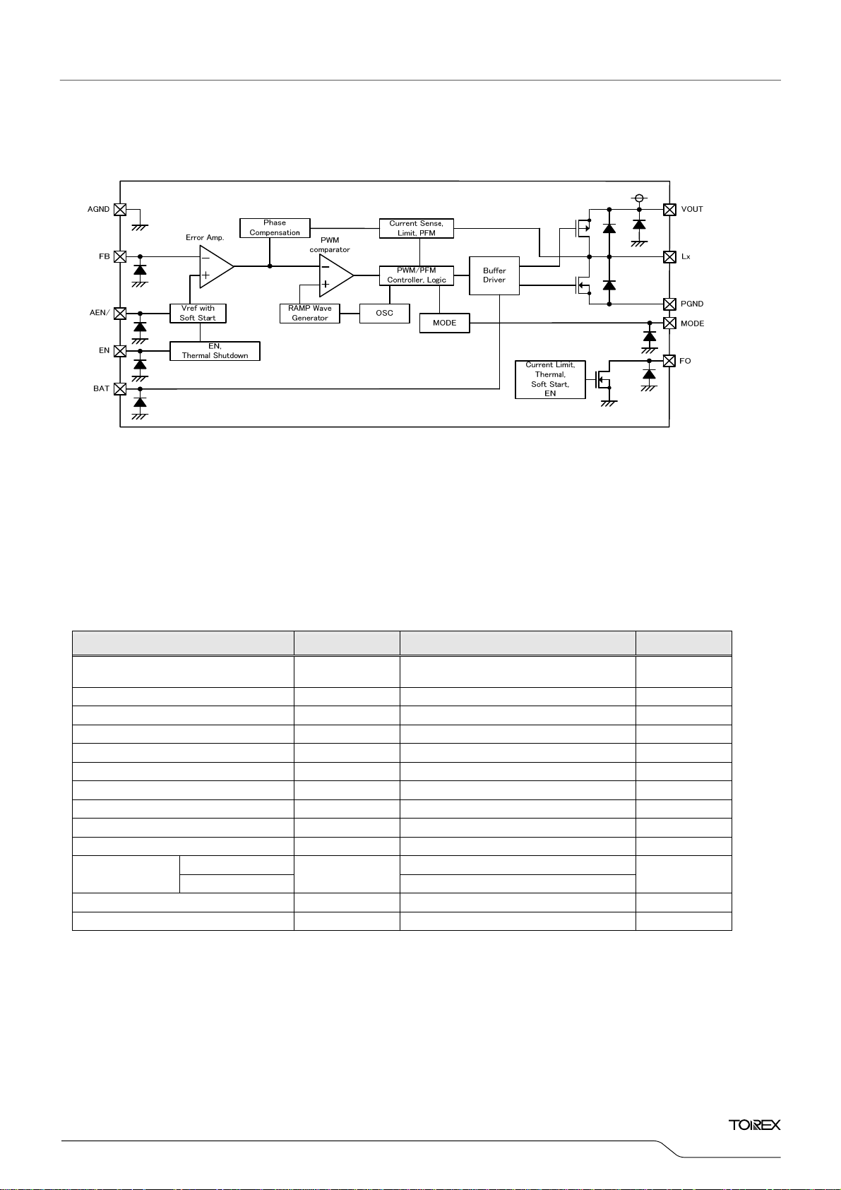
■BLOCK DIAGRAM
●XC9128 Series
* XC9129 Series
The XC9129 series does not have AEN/ pin and FO pin.
■ABSOLUTE MAXIMUM RATINGS
PAR AMETER SYMBOL RATINGS UNITS
V
Pin Voltage VOUT - 0.3~6.5 V
OUT
AEN/ Pin Voltage
FO Pin Voltage
FO Pin Current
FB Pin Voltage VFB - 0.3~6.5 V
BAT Pin Voltage VBAT - 0.3~6.5 V
MODE Pin Voltage VMODE - 0.3~6.5 V
EN Pin Voltage VEN - 0.3~6.5 V
LX Pin Voltage VLx - 0.3~V
LX Pin Current ILx 2000 mA
Power Dissipation
Operating Ambient Temperature Topr - 40~+85
Storage Temperature Tstg - 55~+125
AGND, PGND is the standard voltage for all of voltages.
*1: When implemented on a PCB.
The XC9129 series does not have AEN/ pin and FO pin. These pins are available only in the XC9128 series.
*2:
(*2)
VAEN/ - 0.3~6.5 V
(*2)
VFO - 0.3~6.5 V
(*2)
IFO 10 mA
+0.3 V
OUT
150
(*1)
MSOP-10 350
USP-10B
Pd
XC9128/XC9129
Series
Ta =2 5℃
mW
o
C
o
C
5/26
XC9128/XC9129 Series
■ELECTRICAL CHARACTERISTICS
XC9128/XC9129 Series
LX SW "Nch" ON Resistance RLxN VIN=V
Integral Latch Time (XC9128)
Integral Latch Time (XC9129)
PAR AMETER SYMBOL CONDITIONS MIN. TYP. MAX.
Input Voltage VIN - - - 6.0 V -
FB Voltage VFB
Output Voltage Setting Range VOUTSET - 1.8 - 5.3 V ①
Operation Start Voltage VST1
Oscillation Start Voltage VST2
Operation Hold Voltage VHLD
Supply Current 1 IDD1 VIN = V
Supply Current 2 (XC9128) - 30 80
IDD2
Supply Current 2 (XC9129)
Input Pin Current I
Stand-by Current I
Oscillation Frequency f
Maximum Duty Cycle
Minimum Duty Cycle
BAT
STB
OSC
MAXDTY
MINDTY
PFM Switching Current IPFM
Efficiency
(*2)
EFFI
LX SW "Pch" ON Resistance RLxP
LX Leak Current ILXL VIN=V
Current Limit
(*5)
ILIM V
(*6)
(*6)
tLAT
Soft-Start Time 1 tSS1
Soft-Start Time 2
Soft-Start Time 3
Thermal Shutdown
Temperature
(*7)
tSS2
(*7)
tSS3
T
TSD - - 150 -
Hysteresis Width THYS - - 20 -
Output Voltage Drop
Protection
(*6)
FO Output Current
FO Leakage Current
(*7)
IFO_OUT
(*7)
IFO_Leak VIN = V
V
LVP
×0.9
(*3)
(*8)
(*8)
(*8)
(*8)
(*4)
VEN=0V
,
,
,
V
OUT=VIN
=3.3V, VFO=0V
Voltage to start oscillation during
= 0.46V → 0.44V
V
FB
Connect to external components,
RL=1kΩ
Connect to external components,
RL=33Ω
Voltage to start oscillation during
VIN=0V → 1V, RL=1kΩ
Connect to external components, RL=1kΩ
=3.3V, VFB=0.45V×0.9 - 3 6 mA ②
OUT
VIN = V
OUT
=3.3V
VFB=0.45V×1.1 (Oscillation stop),
V
=0V
MODE
V
V
=3.3V, V
IN
= V
IN
= V
V
IN
VIN = V
VIN = V
=1.8V, VEN=0V - 2 10 μA ③
OUT
=3.3V, VEN=0V - 2 10 μA ②
OUT
=3.3V, VFO=0V
OUT
VFB=0.45V
=3.3V, VFO=0V
OUT
V
=0.45V×0.9
FB
=3.3V, VFO=0V
OUT
VFB=0.45V×1.1
Connect to external components,
V
=0V, RL=330Ω
MODE
Connect to external components,
=33Ω
R
L
VIN=VLx=V
+50mV,
OUT
VFB=0.45V×1.1
=3.3V, Lx =50mV
OUT
= VLX, VFB=0V - 1 - μA ⑤
OUT
>2.5V 1.2 1.5 2.0 A ①
OUT
Time to stop oscillation during
=33Ω → 3.3Ω, VFO=L → H
R
L
Time to stop oscillation during
=33Ω → 3.3Ω
R
L
Time to start oscillation during
→ V
at VIN = V
IN
=3.3V, VFO=0V,
OUT
VFB=0.45V×0.95
VIN = V
=3.3V, VFO=0V,
OUT
VFB=0.45V×0.95
Time to start oscillation during
V
AEN/=VIN
= V
V
IN
OUT
V
→0V.
=3.3V, VFO=0V,
=0.45V×0.8
FB
Time to start oscillation during
V
AEN/=VIN
→0V
VIN =3.3V
Voltage to stop oscillation during
=1.56V→1.3V
V
OUT
VIN =V
=3.3V, VFO=0.25V 1.3 1.7 2.2 mA ④
OUT
=3.3V, VEN=0V ,VFO=1V - 0 1 μA ④
OUT
0.44 0.45 0.46 V ④
- - 0.8 V ①
- - 0.9
- 0.8 - V ①
- 0.7 - V ①
- 28 78
1.02 1.20 1.38 MHz ④
85 92 96 % ④
- - 0 % ④
- 250 400 mA ①
- 93 - % ①
- 0.20
-
0.20
- 3.5 - ms ①
1.7 5.3 10.5 ms ④
- 0.02 0.04 ms ④
1.7 5.3 10.5 ms ④
1.3 1.48 1.56 V ⑥
0.35
(*1)
0.35
Topr=25 oC
UNITS CIRCUIT
(*1)
V ①
μA ②
(*1)
Ω ⑤
(*1)
Ω ⑦
o
C -
o
C -
6/26

)
)
XC9128/XC9129
Series
■ELECTRICAL CHARACTERISTICS (Continued
UNITS
AEN/
=0V
Topr=25oC
CIRCUIT
(*8)
●XC9128/XC9129 Series (Continued
PAR AMETER SYMBOL CONDITIONS MIN. TYP. MAX.
EN "H" Voltage VENH
EN "L" Voltage VENL
MODE "H" Voltage VMODEH RL =330Ω, Voltage operates at PWM control 0.65 - 6.0 V
MODE "L" Voltage VMODEL RL =330Ω, Voltage operates at PFM control AGND - 0.2 V
AEN/ Voltage
EN "H" Current IENH
EN "L" Current IENL
MODE "H" Current IMODEH
MODE "L" Current IMODEL
AEN/ "H" Current
AEN/ "L" Current
FB "H" Current IFBH
FB "L" Current IFBL
Test Conditions:
For the Circuit No.3, unless otherwise stated,
For the Circuit No.7, unless otherwise stated, V
External Components:
*
1 : Designed value
*
2 : Efficiency ={(output voltage) X (output current)} ÷ {(input voltage) X (input current)} X 100
*
3 : LX SW "P-ch" ON resistance=(VLx-V
*
4 : Testing method of LX SW "N-ch" ON resistance is stated at test circuits.
*
5 : Current flowing through the Nch driver transistor is limited.
*
6 : The XC9128D/XC9129D series does not have integral latch protection and V
This is only available with the XC9128B/XC9129B series.
*
7 : The XC9129 series does not have FO and AEN/ pins. These pins are only available in the XC9128 series.
*
8 : The XC9129 series does not have FO and AEN/ pins. The AEN/FO functions are only effective for the test of the XC9128 series.
(*7)
VAEN/
(*7)
IAEN/H
(*7)
IAEN/L
For the Circuit No.1, unless otherwise stated, V
For the Circuit No.2, unless otherwise stated, V
For the Circuit No.4, unless otherwise stated,
For the Circuit No.5, unless otherwise stated,
For the Circuit No.6, unless otherwise stated,
For the Circuit No.1, R
C
For the Circuit No.2,3, C
For the Circuit No.4,6, C
For the Circuit No.5, C
For the Circuit No.7, C
=10μF(ceramic), CIN=10μF(ceramic)
L2
VIN =V
Voltage to start oscillation during
VFB=0.45V×0.9, VEN= 0.2V→0.65V
VIN = V
Voltage to stop oscillation during
VIN = V
Voltage to start oscillation during V
V
V
IN=VOUT=VFB
VIN=V
VIN=V
VIN=V
VIN=V
VIN=V
=270kΩ, R
FB1
=1μF(ceramic)
IN
=1μF(ceramic), Rpull=300Ω
IN
=1μF(ceramic), C
IN
=1μF(ceramic), C
IN
pin test voltage)÷100mA
OUT
=3.3V, VFO=0V
OUT
=3.3V, VFO=0V
OUT
VFB=0.45V×0.9,
V
= 0.65V→0.20V
EN
=3.3V, VFO=0V
OUT
IN=VOUT=VFB=VEN
=6.0V, VEN=0V -0.1 - - μA
OUT=VFB=VMODE
OUT=VFB
OUT
VIN=V
=6.0V, V
OUT=VFB=VAEN/
=6.0V, VEN=0V, V
OUT=VFB
=6.0V, VFB=0V -0.1 - - μA
OUT
=43kΩ, CFB=12pF, L=4.7μH(LTF5022 TDK), CL1=22μF(ceramic),
FB2
=6.0V - - 0.1 μA
OUT
OUT
(*8)
0.65 - 6.0 V ④
(*8)
- - 0.2 V ④
= 0.9V→0.7V
AEN/
0.7 0.8 0.9 V ④
=6.0V - - 0.1 μA
=6.0V - - 0.1 μA
=0V -0.1 - - μA
MODE
=6.0V - - 0.1 μA
=0V -0.1 - - μA
AEN/
=1.8V, VEN=V
IN
=1.8V, VFB =0V, VEN=V
IN
VIN=1.8V, V
VIN=1.8V, VFB=0V, VEN=V
VIN=3.3V, V
VEN=V
MODE
EN=VMODE
MODE=VFO
OUT=VEN=VMODE
=0V
AEN/
=Vpull=VFO=3.3V, VFB=0V
=3.3V
=3.3V, V
MODE
=3.3V, FB=0V
MODE
(*8)
=3.3V, V
=Vpull=VFO=3.3V, V
=1μF(ceramic)
=1μF(ceramic), SBD =XBS304S17(TOREX), Rpull=0.5Ω
function.
LVP
AEN/
=0V
AEN/
(*8)
(*8)
=0V
(*8)
7/26
①
①
②
②
②
②
②
②
②
②
XC9128/XC9129 Series
■TYPICAL APPLICATION CIRCUIT
<Output Voltage Setting>
Output voltage can be set by adding external split resistors. Output voltage is determined by the following equation,
based on the values of R
OUT=0.45 × (RFB1 + RFB2) / RFB2
V
The value of C
the range of 10 kHz to 60 kHz. Adjustments are depending on application, inductance (L), load capacitance (CL) and
dropout voltage.
[Example of calculation]
When R
VOUT1 = 0.45 × (270k+43k ) / 43k = 3.276V
[Typical example]
FB1=270kΩ, RFB2=43kΩ,
VOUT (V)
1.8 300 100 10
2.5 270 59 12
3.3 270 43 12
5.0 180 17.8 15
[External Components]
1.2MHz:
L : 4.7μH (LTF5022-4R7-LC TDK)
: 4.7μH (CDRH4D28C-4R7N SUMIDA)
CL1 : 22μF (ceramic)
CL2 : 10μF (ceramic)
CIN : 10μF (ceramic)
* C
should be selected in 10μF or higher.
L1
Capacitance C
If C
L1
In case of the usage C
check actual performance on the board.
* If using Tantalum or Electrolytic capacitors please be aware that ripple voltage will be higher due to the larger
ESR (Equivalent Series Resistance) values of those types of capacitors. Please also note that the IC’s
operation may become unstable with such capacitors so we recommend that you fully check actual
performance.
, speed-up capacitor for phase compensation, should be f
FB
is lower than 10μF, operation may be unstable.
8/26
FB1 and RFB2. The sum of RFB1 and RFB2 should normally be 500k or less.
= 1 / (2 x
ZFB
RFB1 (kΩ) RFB2 (kΩ)
+ CL2 is recommended 30μF or higher. (Ceramic capacitor compatible)
L1
L1
+ C
<30μF, output ripple may increase so that we recommend that you fully
L2
CFB (pF)
x
CFB1 x RFB1) which is in
 Loading...